EP4224666A1 - Wireless charging apparatus - Google Patents
Wireless charging apparatus Download PDFInfo
- Publication number
- EP4224666A1 EP4224666A1 EP22862331.0A EP22862331A EP4224666A1 EP 4224666 A1 EP4224666 A1 EP 4224666A1 EP 22862331 A EP22862331 A EP 22862331A EP 4224666 A1 EP4224666 A1 EP 4224666A1
- Authority
- EP
- European Patent Office
- Prior art keywords
- cavity
- thermally conductive
- conductive member
- housing
- fan
- Prior art date
- Legal status (The legal status is an assumption and is not a legal conclusion. Google has not performed a legal analysis and makes no representation as to the accuracy of the status listed.)
- Granted
Links
Images




Classifications
-
- H—ELECTRICITY
- H02—GENERATION; CONVERSION OR DISTRIBUTION OF ELECTRIC POWER
- H02J—ELECTRIC POWER NETWORKS; CIRCUIT ARRANGEMENTS OR SYSTEMS FOR SUPPLYING OR DISTRIBUTING ELECTRIC POWER; SYSTEMS FOR STORING ELECTRIC ENERGY
- H02J7/00—Circuit arrangements for charging or discharging batteries or for supplying loads from batteries
- H02J7/60—Circuit arrangements for charging or discharging batteries or for supplying loads from batteries including safety or protection arrangements
- H02J7/65—Circuit arrangements for charging or discharging batteries or for supplying loads from batteries including safety or protection arrangements against overtemperature
-
- H—ELECTRICITY
- H02—GENERATION; CONVERSION OR DISTRIBUTION OF ELECTRIC POWER
- H02J—ELECTRIC POWER NETWORKS; CIRCUIT ARRANGEMENTS OR SYSTEMS FOR SUPPLYING OR DISTRIBUTING ELECTRIC POWER; SYSTEMS FOR STORING ELECTRIC ENERGY
- H02J50/00—Circuit arrangements or systems for wireless supply or distribution of electric power
- H02J50/005—Mechanical details of housing or structure aiming to accommodate the power transfer means, e.g. mechanical integration of coils, antennas or transducers into emitting or receiving devices
-
- H—ELECTRICITY
- H02—GENERATION; CONVERSION OR DISTRIBUTION OF ELECTRIC POWER
- H02J—ELECTRIC POWER NETWORKS; CIRCUIT ARRANGEMENTS OR SYSTEMS FOR SUPPLYING OR DISTRIBUTING ELECTRIC POWER; SYSTEMS FOR STORING ELECTRIC ENERGY
- H02J50/00—Circuit arrangements or systems for wireless supply or distribution of electric power
- H02J50/10—Circuit arrangements or systems for wireless supply or distribution of electric power using inductive coupling
-
- H—ELECTRICITY
- H02—GENERATION; CONVERSION OR DISTRIBUTION OF ELECTRIC POWER
- H02J—ELECTRIC POWER NETWORKS; CIRCUIT ARRANGEMENTS OR SYSTEMS FOR SUPPLYING OR DISTRIBUTING ELECTRIC POWER; SYSTEMS FOR STORING ELECTRIC ENERGY
- H02J7/00—Circuit arrangements for charging or discharging batteries or for supplying loads from batteries
- H02J7/70—Circuit arrangements for charging or discharging batteries or for supplying loads from batteries characterised by the mechanical construction
- H02J7/731—Circuit arrangements for charging or discharging batteries or for supplying loads from batteries characterised by the mechanical construction specially adapted for holding portable devices containing batteries
-
- H—ELECTRICITY
- H05—ELECTRIC TECHNIQUES NOT OTHERWISE PROVIDED FOR
- H05K—PRINTED CIRCUITS; CASINGS OR CONSTRUCTIONAL DETAILS OF ELECTRIC APPARATUS; MANUFACTURE OF ASSEMBLAGES OF ELECTRICAL COMPONENTS
- H05K7/00—Constructional details common to different types of electric apparatus
- H05K7/20—Modifications to facilitate cooling, ventilating, or heating
- H05K7/20009—Modifications to facilitate cooling, ventilating, or heating using a gaseous coolant in electronic enclosures
- H05K7/20136—Forced ventilation, e.g. by fans
- H05K7/20145—Means for directing air flow, e.g. ducts, deflectors, plenum or guides
-
- Y—GENERAL TAGGING OF NEW TECHNOLOGICAL DEVELOPMENTS; GENERAL TAGGING OF CROSS-SECTIONAL TECHNOLOGIES SPANNING OVER SEVERAL SECTIONS OF THE IPC; TECHNICAL SUBJECTS COVERED BY FORMER USPC CROSS-REFERENCE ART COLLECTIONS [XRACs] AND DIGESTS
- Y02—TECHNOLOGIES OR APPLICATIONS FOR MITIGATION OR ADAPTATION AGAINST CLIMATE CHANGE
- Y02B—CLIMATE CHANGE MITIGATION TECHNOLOGIES RELATED TO BUILDINGS, e.g. HOUSING, HOUSE APPLIANCES OR RELATED END-USER APPLICATIONS
- Y02B40/00—Technologies aiming at improving the efficiency of home appliances, e.g. induction cooking or efficient technologies for refrigerators, freezers or dish washers
Definitions
- Embodiments of this application relate to the field of wireless charging technologies, and in particular, to a wireless charging device.
- a large amount of heat is generated by the electronic device. If charging time is relatively long, the heat may cause damage to both the electronic device and a wireless charging device.
- An existing low-power wireless charging device is not provided with a heat dissipation structure, or dissipates heat of the electronic device by being in contact with a heat sink; and a high-power wireless charging device dissipates heat of the electronic device by using a fan.
- a heat dissipation effect is not ideal, and needs to be further optimized.
- this application provides a wireless charging device with a good heat dissipation effect.
- this application provides a wireless charging device for charging an electronic device.
- the wireless charging device includes a housing, a transmit coil, and a heat dissipation assembly.
- the housing is provided with a panel.
- the transmit coil is disposed in the housing, and is located on a side of the panel.
- the housing is configured to place an electronic device to be charged, and the electronic device is at a distance from the panel.
- the housing is provided with an air vent located under the panel.
- the heat dissipation assembly includes a semiconductor refrigeration chip and a fan.
- the semiconductor refrigeration chip includes a cold end and a hot end. The hot end is disposed on the housing.
- the fan is disposed on the housing, and air blown by the fan passes through the cold end and is blown out from the air vent.
- the air blown by the fan passes through the cold end and a temperature of the air is reduced, and the air passes between the panel and the electronic device to reduce a temperature of the electronic device.
- the heat dissipation assembly further includes another fan and a first thermally conductive member.
- the first thermally conductive member is disposed on a side that is of the transmit coil and that is away from the panel; and the another fan is disposed on the housing, and blows air to the first thermally conductive member.
- the air blown by the another fan can be blown to the first thermally conductive member, so as to reduce a temperature of the first thermally conductive member, and then reduce a temperature of the transmit coil.
- the first thermally conductive member is obliquely disposed above the another fan, and the another fan blows air from an upper side.
- the first thermally conductive member is obliquely disposed above the fan, to increase projection of the first thermally conductive member on the fan, so that the air blown by the fan may be directly blown to a larger area of the first thermally conductive member, thereby improving efficiency of reducing the temperature of the first thermally conductive member.
- the heat dissipation assembly further includes another semiconductor refrigeration chip, and the another semiconductor refrigeration chip is disposed between the transmit coil and the first thermally conductive member, and the cold end faces the transmit coil and the hot end faces the first thermally conductive member.
- the another semiconductor refrigeration chip is disposed between the transmit coil and the first thermally conductive member, thereby further improving cooling efficiency of the transmit coil.
- a first cavity and a second cavity are disposed in the housing, and the second cavity is located above the first cavity.
- the fan and the another fan are disposed in the first cavity.
- the transmit coil, the semiconductor refrigeration chip, and the first thermally conductive member are sequentially disposed in the second cavity.
- the air blown by the fan and the air blown by the another fan are respectively blown to the first thermally conductive member and between the electronic device and the panel, so that both the electronic device and the wireless charging device are cooled, thereby improving cooling efficiency.
- the first cavity includes a first segment and a second segment, the second segment extends upward along a curve from the first segment to the air vent, the fan is located in the first segment, and the semiconductor refrigeration chip is located in the second segment.
- the second segment extends upward along a curve from the first segment to the air vent, so as to guide the air blown by the fan to be blown out from the air vent, and reduce a force of the air blown by the air vent on the electronic device placed on the housing.
- the wireless charging device further includes a circuit board
- the housing is further provided with a third cavity and an air exhaust vent that communicate with each other, and the third cavity communicates with both the first cavity and the second cavity.
- the third cavity is located above the first cavity, and is located on a side of the second cavity.
- the circuit board is electrically connected to the transmit coil, the fan, and the another fan.
- the circuit board is disposed on the housing, and is located in the third cavity. The air blown by the another fan can be blown to the first thermally conductive member and the circuit board, and is discharged from the air exhaust vent.
- the another fan can also blow air to the circuit board, so that a temperature of the circuit board is reduced, and a cooling effect of the wireless charging device is further improved.
- this application provides a wireless charging device, where the wireless charging device includes a housing, a transmit coil, and a heat dissipation assembly.
- the housing is provided with a panel.
- the heat dissipation assembly includes a semiconductor refrigeration chip, a first thermally conductive member, and a fan.
- the semiconductor refrigeration chip includes a cold end and a hot end.
- the panel, the transmit coil, the semiconductor refrigeration chip, and the first thermally conductive member are sequentially stacked.
- the cold end faces the transmit coil
- the hot end faces the first thermally conductive member.
- the fan is disposed in the housing, and the first thermally conductive member is obliquely disposed above the fan.
- the air blown by the fan reduces a temperature of the first thermally conductive member, to improve a cooling effect of a cold end of the semiconductor refrigeration chip that is in contact with the first thermally conductive member, and reduce temperatures of the transmit coil and the panel that are sequentially in contact with the cold end, thereby reducing a temperature of the electronic device that is in contact with the panel.
- a first cavity and a second cavity are disposed in the housing, and the second cavity is located above the first cavity.
- the fan is located in the first cavity.
- the transmit coil, the semiconductor refrigeration chip, and the first thermally conductive member are sequentially disposed in the second cavity.
- the third cavity is located above the first cavity, and is located on a side of the second cavity, to enable the air blown by the fan to enter the third cavity from the first cavity and be directly blown to the first thermally conductive member, so as to effectively reduce a temperature of the hot end of the semiconductor refrigeration chip, so that a temperature of the cold end of the semiconductor refrigeration chip is maintained at a lower temperature, or a low-temperature state is maintained for a longer time.
- the wireless charging device further includes a circuit board
- the housing is further provided with a third cavity and an air exhaust vent that communicate with each other, and the third cavity communicates with both the first cavity and the second cavity.
- the third cavity is located above the first cavity, and is located on a side of the second cavity.
- the circuit board is electrically connected to the transmit coil and the fan.
- the circuit board is disposed on the housing, and is located in the third cavity. The air blown by the fan can be blown to the first thermally conductive member and the circuit board, and is discharged from the air exhaust vent.
- the fan can also blow air to the circuit board, so that a temperature of the circuit board is reduced, and a cooling effect of the wireless charging device is further improved.
- the wireless charging device further includes a second thermally conductive member, and the second thermally conductive member is disposed between the transmit coil and the semiconductor refrigeration chip.
- the second thermally conductive member can conduct all heat of the transmit coil parallel to a surface of the panel, and then conduct the heat to the semiconductor refrigeration chip, thereby improving cooling efficiency.
- the heat dissipation assembly further includes a third thermally conductive member, and the third thermally conductive member is disposed between the semiconductor refrigeration chip and the first thermally conductive member.
- the third thermally conductive member can conduct all heat of the hot end parallel to the panel, and then conduct the heat to the first thermally conductive member, thereby improving cooling efficiency.
- the second thermally conductive member or the third thermally conductive member is a thermally conductive structure made of a thermally conductive material that is deformable under pressure.
- the second thermally conductive member is pressed by the transmit coil and the semiconductor refrigeration chip to deform, so as to be evenly in contact with both the transmit coil and the semiconductor refrigeration chip, thereby improving heat conduction efficiency.
- the third thermally conductive member is a thermally conductive structure made of a thermally conductive material that is deformable under pressure. The third thermally conductive member is pressed by the first thermally conductive member and the semiconductor refrigeration chip to deform, so as to be evenly in contact with both the first thermally conductive member and the semiconductor refrigeration chip, thereby improving heat conduction efficiency.
- Wireless charging device 100, 100a, 100b; Housing: 10, 10a, 10b; Panel: 11; Support part: 12; Spacing part: 13; Air vent: 101; First cavity: 102; First segment: 1021; Second segment: 1022; Second cavity: 103; Third cavity: 104; Air intake vent: 105; Air exhaust vent: 106; Fastener: 14; Transmit coil: 20; Coil body: 21; Soft magnet: 23; Heat dissipation assembly: 30; Semiconductor refrigeration chip: 31, 31a, 31b; Cold end: 311, 311a, 311b; Hot end: 312, 312a, 312b; Fan: 32, 32a, 32b; First thermally conductive member: 33; Second thermally conductive member: 34; Third thermally conductive member: 35; Circuit board: 40; Electronic device: 200.
- the wireless charging device 100 is configured to charge an electronic device 200.
- the electronic device 200 may be a mobile phone, a tablet personal computer (Tablet Personal Computer), a laptop computer (Laptop Computer), a personal digital assistant (Personal Digital Assistant, PDA), a mobile Internet device (Mobile Internet Device, MID), a wearable device (Wearable Device), or the like.
- the wireless charging device 100 includes a housing 10, a transmit coil 20, and a heat dissipation assembly 30.
- a first cavity 102 and a second cavity 103 are disposed in the housing 10.
- the second cavity 103 is located above the first cavity 102.
- the housing 10 is provided with a panel 11.
- the transmit coil 20 is disposed in the first cavity 102, and is in contact with one side of the panel 11.
- the wireless charging device 100 generates an alternating current electromagnetic field when the transmit coil 20 is connected to an alternating current power supply, so that a coil in the electronic device 200 generates an inducting voltage in the alternating current magnetic field, thereby implementing wireless charging on the electronic device 200.
- the electronic device 200 is placed on the housing 10, and the electronic device 200 is at a distance from the panel 11, as shown in FIG. 1 .
- the heat dissipation assembly 30 includes a semiconductor refrigeration chip 31 and a fan 32.
- the semiconductor refrigeration chip 31 and the fan 32 are separately disposed in the first cavity 102.
- the housing 10 is further provided with an air vent 101 communicating with the first cavity 102.
- the air vent 101 is located under the panel 11.
- the semiconductor refrigeration chip 31 is made based on a Peltier (Peltier) effect of a semiconductor material.
- the Peltier effect refers to a phenomenon that one end absorbs heat and the other end dissipates heat when a direct current passes through a galvanic couple formed by two different semiconductor materials in series.
- the semiconductor refrigeration chip 31 made based on this principle includes a cold end 311 and a hot end 312 that are on opposite sides.
- the cold end 311 may cool adjacent components, and heat is transferred through the hot end 312.
- the semiconductor refrigeration chip 31 is disposed on the housing 10, and is located in the first cavity 102.
- the hot end 312 of the semiconductor refrigeration chip 31 is fixedly connected to the housing 10, and the cold end 311 protrudes into the first cavity 102.
- the air blown by the fan 32 passes through the cold end 311 and is blown out from the air vent 101.
- a temperature of the air that passes through the cold end 311 is reduced, and the air passes between the panel 11 and the electronic device 200 to reduce a temperature of the electronic device 200.
- the panel 11 is made of an insulating and heat-insulation material (for example, a glass fiber or a vacuum plate). Heat generated by the transmit coil 20 is not conducted between the panel 11 and the electronic device 200 through the panel 11, so that cooling of the electronic device 200 by the air blown from the air vent 101 is improved.
- an insulating and heat-insulation material for example, a glass fiber or a vacuum plate.
- the panel 11 may alternatively be made of an insulating and thermally conductive non-metallic material, such as a carbon fiber material or a ceramic material.
- the air blown from the air vent 101 may cool both the panel 11 and the electronic device 200, and the cooling of the panel 11 reduces a temperature of the transmit coil 20.
- the fan 32 and the semiconductor refrigeration chip 31 are located in the first cavity 102.
- the semiconductor refrigeration chip 31 is closer to the air vent 101 than the fan 32.
- An air intake vent 105 is disposed at the bottom of the housing 10.
- the air intake vent 105 is located on a side that is of the first cavity 102 and that is away from the second cavity 103.
- the air intake vent 105 communicates with the first cavity 102. Air enters the first cavity 102 from the air intake vent 105, and the fan 32 guides the air to blow between the electronic device 200 and the panel 11 through the air vent.
- the air intake vent 105 may alternatively be disposed on a side that is of the first cavity 102 and that is away from the air vent 101.
- a position of the air intake vent 105 on the first cavity 102 may be set based on an air guiding direction of the fan 32, provided that the fan 32 can guide air entering from the air intake vent 105 to be blown out of the air vent 101.
- the two semiconductor refrigeration chips 31 are disposed opposite to each other on two opposite cavity walls of the first cavity 102, and cold ends 311 of the two semiconductor refrigeration chips are disposed opposite to each other.
- the air blown by the fan 32 is blown to the cold ends 311 of the two semiconductor refrigeration chips 31, so that the air blown between the electronic device 200 and the panel 11 is quickly cooled, thereby improving efficiency of reducing a temperature of the electronic device 200.
- the housing 10 is further provided with a support part 12 on a side of the air vent 101.
- the support part 12 is configured to support the electronic device 200.
- the housing 10 is further provided with a spacing part 13. There are two spacing parts 13. The two spacing parts 13 are disposed at intervals and protrude from the panel 11. The spacing part 13 is configured to be in contact with the electronic device 200, so that there is a distance between the electronic device 200 and the panel 11.
- a quantity of spacing parts 13 may be one or another number. Provided that the spacing part 13 protrudes from the panel 11, the electronic device 200 is placed on the housing 10, and is in contact with the spacing part 13, so that there is a distance between the electronic device 200 and the panel 11.
- the first cavity 102 includes a first segment 1021 and a second segment 1022 that communicate with each other.
- the fan 32 is disposed in the first segment 1021.
- the second segment 1022 is closer to the air vent 101 than the first segment 1021.
- the second segment 1022 extends upward along a curve from the first segment 1021 to the air vent 101, so as to guide the air blown by the fan 32 to blow out from the air vent 101, and reduce a force of the air blown by the air vent 101 on the electronic device 200 placed on the housing 10.
- the fan 32 blows air in a direction of the first segment 1021 toward the second segment 1022.
- first segment 1021 may alternatively be obliquely disposed along a straight line, or the first segment 1021 extends from the second segment 1022 to the air vent 101 along two straight paths that intersect along an L-shape or a V-shape.
- the heat dissipation assembly 30 further includes a first thermally conductive member 33.
- the first thermally conductive member 33 is disposed on the housing 10, and is located in the first cavity 102.
- the panel 11, the transmit coil 20, and the first thermally conductive member 33 are sequentially stacked, and sequentially transmit heat.
- the first thermally conductive member 33 may be separated from the housing 10, and the first thermally conductive member 33 is exposed from the housing 10 and is in contact with air outside the housing 10.
- the first thermally conductive member 33 may be in an integrated structure with the housing 10, and the first thermally conductive member 33 is in contact with the air outside the housing 10.
- Heat of the transmit coil 20 is conducted to the first thermally conductive member 33, and the first thermally conductive member 33 dissipates the heat to the outside of the first cavity 102.
- first thermally conductive member 33 may alternatively be omitted.
- the transmit coil 20 includes a coil body 21 and a soft magnet 23.
- the panel 11, the coil body 21, and the soft magnet 23 are sequentially disposed.
- the soft magnet 23 can improve strength of a magnetic field generated when the coil body 21 is energized.
- the soft magnet 23 is made of a soft magnetic material, for example, the soft magnet 23 may be made of a ferrite or an iron-based amorphous alloy.
- the transmit coil 20 and the first thermally conductive member 33 may be separately connected to the housing 10 in an adhesive manner, but is not limited thereto.
- the first thermally conductive member 33 is locked on the housing 10 by using a fastener 14 such as a screw, so that the first thermally conductive member 33 and the panel 11 are respectively pressed against both sides of the transmit coil 20, and the transmit coil 20 and the first thermally conductive member 33 are fastened to the housing 10, thereby avoiding impact of heat-conducting property of adhesive on heat conduction efficiency of the transmit coil 20 and the first thermally conductive member 33.
- the wireless charging device 100 further includes a circuit board 40.
- the circuit board 40 is disposed on the housing 10, and is located in the first cavity 102.
- the circuit board 40 is located on a side that is of the fan 32 and that is away from the air intake vent 105, and the circuit board 40 is electrically connected to the transmit coil 20, the fan 32, and the semiconductor refrigeration chip 31, so as to control the transmit coil 20, the fan 32, and the semiconductor refrigeration chip 31 to operate.
- the air blown by the fan 32 passes through the cold end 311 of the semiconductor refrigeration chip 31, so that the air cools down and passes through the air vent 101 to flow between the panel 11 and the electronic device 200, thereby improving a cooling effect of the electronic device 200.
- a difference between a wireless charging device 100a in another embodiment and the wireless charging device 100 lies in that the wireless charging device 100a further includes another fan 32a and another semiconductor refrigeration chip 31a, and a structure of a housing 10 of the wireless charging device 100a is different from a structure of a housing 10a of the wireless charging device 100a.
- the semiconductor refrigeration chip 31a is stacked on a side of a transmit coil 20 and a first thermally conductive member 33.
- the fan 32a is disposed on a first housing, and is located in a first cavity 102, but is not limited thereto.
- the fan 32a is located on a side that is of the fan 32a and that is away from the semiconductor refrigeration chip 31a.
- the housing 10a is further provided with a third cavity 104 and an air exhaust vent 106.
- the third cavity 104 communicates with both the first cavity 102 and a second cavity 103.
- the third cavity 104 is located above the first cavity 102, and is located on a side of the second cavity 103.
- the air exhaust vent 106 is located on a side that is of the third cavity 104 and that is away from the first thermally conductive member 33.
- the air blown by the fan 32a can be blown to the first thermally conductive member 33 and discharged from the air exhaust vent 106, thereby reducing a temperature of the first thermally conductive member 33, and then reducing a temperature of the transmit coil 20.
- the first thermally conductive member 33 is obliquely disposed above the fan 32a, to increase projection of the first thermally conductive member 33 on the fan 32a, so that the air blown by the fan 32a may be directly blown to a larger area of the first thermally conductive member 33, thereby improving efficiency of reducing the temperature of the first thermally conductive member 33.
- the air blown by the fan 32a and the air blown by the fan 32 respectively are respectively blown to the first thermally conductive member 33 and between the electronic device 200 and the panel 11, so that both the electronic device 200 and the wireless charging device 100 are cooled, thereby improving cooling efficiency.
- the wireless charging device 100a further includes a circuit board 40.
- the circuit board 40 is disposed on the housing 10a, and is located on a cavity wall that is of the third cavity 104 and that is away from the first thermally conductive member 33.
- the circuit board 40 is electrically connected to the transmit coil 20, the fan 32a, and the fan 32a.
- the circuit board 40 is obliquely disposed above the fan 32a, so that the air blown by the fan 32a can be blown to the circuit board 40, and the circuit board 40 is cooled.
- the wireless charging device 100a further includes a second thermally conductive member 34, and the second thermally conductive member 34 is disposed between the transmit coil 20 and the semiconductor refrigeration chip 31a.
- the second thermally conductive member 34 is a thermally conductive structure made of a thermally conductive material that is deformable under pressure.
- the second thermally conductive member 34 is a sheet-like structure made of thermally conductive silicone. Hardness of the transmit coil 20 and hardness of the semiconductor refrigeration chip 31a are greater than hardness of the second thermally conductive member 34.
- the second thermally conductive member 34 is pressed by the transmit coil 20 and the semiconductor refrigeration chip 31a to deform, so as to be evenly in contact with both the transmit coil 20 and the semiconductor refrigeration chip 31a, thereby improving heat conduction efficiency.
- the second thermally conductive member 34 may alternatively be made of a hard thermally conductive material.
- the second thermally conductive member 34 can conduct all heat of the transmit coil 20 parallel to the panel 11, and then conduct the heat to the semiconductor refrigeration chip 31a, thereby improving cooling efficiency.
- both the first thermally conductive member 33 and the second thermally conductive member 34 may be omitted.
- the heat dissipation assembly 30 further includes a third thermally conductive member 35, and the third thermally conductive member 35 is disposed between the semiconductor refrigeration chip 31a and the first thermally conductive member 33.
- the third thermally conductive member 35 is a thermally conductive structure made of a thermally conductive material that is deformable under pressure. The third thermally conductive member 35 is pressed by the first thermally conductive member 33 and the semiconductor refrigeration chip 31a to deform, so as to be evenly in contact with both the first thermally conductive member 33 and the semiconductor refrigeration chip 31a, thereby improving heat conduction efficiency.
- the semiconductor refrigeration chip 31a may alternatively be omitted. Heat of the transmit coil 20 is conducted to the first thermally conductive member 33, and the fan 32a blows air to the first thermally conductive member 33, which can also reduce a temperature of the first thermally conductive member 33.
- the air blown by the fan 32 passes through the cold end 311 of the semiconductor refrigeration chip 31, so that the air cools down and passes through the air vent 101 to flow between the panel 11 and the electronic device 200, thereby improving a cooling effect of the electronic device 200.
- the air is blown to the first thermally conductive member 33 through the fan 32a, a temperature of the transmit coil 20 is reduced through heat conduction between the first thermally conductive member 33 and the transmit coil 20.
- the wireless charging device 100a can cool both the electronic device 200 and the transmit coil 20.
- a wireless charging device 100b includes a housing 10ab, a transmit coil 20, and a heat dissipation assembly 30.
- the housing 10ab is provided with a panel 11.
- the heat dissipation assembly 30 includes a semiconductor refrigeration chip 31b, a first thermally conductive member 33, and a fan 32b.
- the semiconductor refrigeration chip 31b includes a cold end 311b and a hot end 312b.
- the panel 11, the transmit coil 20, the semiconductor refrigeration chip 31b, and the first thermally conductive member 33 are sequentially stacked.
- the cold end 311b faces the transmit coil 20.
- the hot end 312b faces the first thermally conductive member 33.
- the fan 32b is disposed in the housing 10ab.
- the first thermally conductive member 33 is obliquely disposed above the fan 32b, to increase projection of the first thermally conductive member 33 on the fan 32b, so that the air blown by the fan 32b may be directly blown to a larger area of the first thermally conductive member 33, thereby improving efficiency of reducing a temperature of the first thermally conductive member 33.
- the panel 11 is made of an insulating and thermally conductive non-metallic material, such as a carbon fiber material or a ceramic material.
- the housing 10ab is further provided with a support part 12 located under the panel 11.
- the support part 12 is configured to support the electronic device 200, so that the electronic device 200 is placed on the housing 10ab, and is in contact with the panel 11.
- the air blown by the fan 32b reduces a temperature of the first thermally conductive member 33, to improve a cooling effect of the cold end 311b of the semiconductor refrigeration chip 31b that is in contact with the first thermally conductive member 33, and then reduce temperatures of the transmit coil 20 and the panel 11 that are sequentially in contact with the cold end 311b, thereby reducing a temperature of the electronic device 200 that is in contact with the panel 11.
- a first cavity 102, a second cavity 103, and a third cavity 104 are disposed in the housing 10ab.
- the second cavity 103 is located above the first cavity 102.
- the fan 32b is located in the first cavity 102.
- the transmit coil 20, the semiconductor refrigeration chip 31b, and the first thermally conductive member 33 are sequentially disposed in the second cavity 103.
- the housing 10ab is further provided with an air exhaust vent 106, and the air exhaust vent 106 communicates with the third cavity 104.
- An air intake vent 105 communicating with the first cavity 102 is disposed at the bottom of the housing 10ab.
- the third cavity 104 communicates with both the first cavity 102 and a second cavity 103.
- the third cavity 104 is located above the first cavity 102, and is located on a side of the second cavity 103, to enable the air blown by the fan 32b to enter the third cavity 104 from the first cavity 102 and be directly blown to the first thermally conductive member 33, so as to effectively reduce a temperature of the hot end 312b of the semiconductor refrigeration chip 31b, so that a temperature of the cold end 311b of the semiconductor refrigeration chip 31b is maintained at a lower temperature, or a low-temperature state is maintained for a longer time.
- the wireless charging device 100b further includes a circuit board 40.
- the circuit board 40 is disposed on the housing 10ab, and is located in the third cavity 104.
- the circuit board 40 is electrically connected to the transmit coil 20 and the fan 32b.
- the circuit board 40 is obliquely disposed above the fan 32b, so that the air blown by the fan 32b can be blown to the circuit board 40, and the circuit board 40 is cooled.
- the wireless charging device 100b further includes a second thermally conductive member 34, and the second thermally conductive member 34 is disposed between the transmit coil 20 and the semiconductor refrigeration chip 31b.
- the second thermally conductive member 34 is a thermally conductive structure made of a thermally conductive material that is deformable under pressure.
- the second thermally conductive member 34 is a sheet-like structure made of thermally conductive silicone. Hardness of the transmit coil 20 and hardness of the semiconductor refrigeration chip 31b are greater than hardness of the second thermally conductive member 34.
- the second thermally conductive member 34 is pressed by the transmit coil 20 and the semiconductor refrigeration chip 31b to deform, so as to be evenly in contact with both the transmit coil 20 and the semiconductor refrigeration chip 31b, thereby improving heat conductive efficiency.
- the second thermally conductive member 34 may alternatively be made of a hard thermally conductive material.
- the second thermally conductive member 34 can conduct all heat of the transmit coil 20 parallel to the panel 11, and then conduct the heat to the semiconductor refrigeration chip 31b, thereby improving cooling efficiency.
- both the first thermally conductive member 33 and the second thermally conductive member 34 may be omitted.
- the heat dissipation assembly 30 further includes a third thermally conductive member 35, and the third thermally conductive member 35 is disposed between the semiconductor refrigeration chip 31b and the first thermally conductive member 33.
- the third thermally conductive member 35 can conduct all heat of the hot end 312b parallel to the panel 11, and then conduct the heat to the first thermally conductive member 33, thereby improving cooling efficiency.
- the third thermally conductive member 35 is a thermally conductive structure made of a thermally conductive material that is deformable under pressure.
- the third thermally conductive member 35 is pressed by the first thermally conductive member 33 and the semiconductor refrigeration chip 31b to deform, so as to be evenly in contact with both the first thermally conductive member 33 and the semiconductor refrigeration chip 31b, thereby improving heat conductive efficiency.
- the wireless charging device 100b cools the transmit coil 20, the panel 11, and the electronic device 200 that are sequentially in contact with each other through the cold end 311b of the semiconductor refrigeration chip 31b, and the fan 32b blows air to the first thermally conductive member 33, so that the hot end 312b that is in contact with the first thermally conductive member 33 is cooled, thereby improving a cooling effect.
- the wireless charging device 100, the wireless charging device 100a, and the wireless charging device 100b may charge the electronic device, and a heat dissipation effect is good in a charging process.
- the electronic device is a mobile phone, a tablet computer, a headset, a headset case, or a smartwatch.
Landscapes
- Engineering & Computer Science (AREA)
- Power Engineering (AREA)
- Computer Networks & Wireless Communication (AREA)
- Microelectronics & Electronic Packaging (AREA)
- Physics & Mathematics (AREA)
- Thermal Sciences (AREA)
- Cooling Or The Like Of Electrical Apparatus (AREA)
- Charge And Discharge Circuits For Batteries Or The Like (AREA)
Abstract
Description
- This application claims priority to
Chinese Patent Application No. 202123159198.2, filed with the China National Intellectual Property Administration on December 14, 2021 - Embodiments of this application relate to the field of wireless charging technologies, and in particular, to a wireless charging device.
- In a wireless charging process of an electronic device, a large amount of heat is generated by the electronic device. If charging time is relatively long, the heat may cause damage to both the electronic device and a wireless charging device. An existing low-power wireless charging device is not provided with a heat dissipation structure, or dissipates heat of the electronic device by being in contact with a heat sink; and a high-power wireless charging device dissipates heat of the electronic device by using a fan. However, a heat dissipation effect is not ideal, and needs to be further optimized.
- In view of this, this application provides a wireless charging device with a good heat dissipation effect.
- According to a first aspect, this application provides a wireless charging device for charging an electronic device. The wireless charging device includes a housing, a transmit coil, and a heat dissipation assembly. The housing is provided with a panel. The transmit coil is disposed in the housing, and is located on a side of the panel. The housing is configured to place an electronic device to be charged, and the electronic device is at a distance from the panel. The housing is provided with an air vent located under the panel. The heat dissipation assembly includes a semiconductor refrigeration chip and a fan. The semiconductor refrigeration chip includes a cold end and a hot end. The hot end is disposed on the housing. The fan is disposed on the housing, and air blown by the fan passes through the cold end and is blown out from the air vent.
- The air blown by the fan passes through the cold end and a temperature of the air is reduced, and the air passes between the panel and the electronic device to reduce a temperature of the electronic device.
- In a possible implementation, the heat dissipation assembly further includes another fan and a first thermally conductive member. The first thermally conductive member is disposed on a side that is of the transmit coil and that is away from the panel; and the another fan is disposed on the housing, and blows air to the first thermally conductive member.
- Apparently, in the foregoing implementation, the air blown by the another fan can be blown to the first thermally conductive member, so as to reduce a temperature of the first thermally conductive member, and then reduce a temperature of the transmit coil.
- In a possible implementation, the first thermally conductive member is obliquely disposed above the another fan, and the another fan blows air from an upper side.
- Apparently, in the foregoing implementation, the first thermally conductive member is obliquely disposed above the fan, to increase projection of the first thermally conductive member on the fan, so that the air blown by the fan may be directly blown to a larger area of the first thermally conductive member, thereby improving efficiency of reducing the temperature of the first thermally conductive member.
- In a possible implementation, the heat dissipation assembly further includes another semiconductor refrigeration chip, and the another semiconductor refrigeration chip is disposed between the transmit coil and the first thermally conductive member, and the cold end faces the transmit coil and the hot end faces the first thermally conductive member.
- Apparently, in the foregoing implementation, the another semiconductor refrigeration chip is disposed between the transmit coil and the first thermally conductive member, thereby further improving cooling efficiency of the transmit coil.
- In a possible implementation, a first cavity and a second cavity are disposed in the housing, and the second cavity is located above the first cavity. The fan and the another fan are disposed in the first cavity. The transmit coil, the semiconductor refrigeration chip, and the first thermally conductive member are sequentially disposed in the second cavity.
- Apparently, in the foregoing implementation, the air blown by the fan and the air blown by the another fan are respectively blown to the first thermally conductive member and between the electronic device and the panel, so that both the electronic device and the wireless charging device are cooled, thereby improving cooling efficiency.
- In a possible implementation, the first cavity includes a first segment and a second segment, the second segment extends upward along a curve from the first segment to the air vent, the fan is located in the first segment, and the semiconductor refrigeration chip is located in the second segment.
- Apparently, in the foregoing implementation, the second segment extends upward along a curve from the first segment to the air vent, so as to guide the air blown by the fan to be blown out from the air vent, and reduce a force of the air blown by the air vent on the electronic device placed on the housing.
- In a possible implementation, the wireless charging device further includes a circuit board, the housing is further provided with a third cavity and an air exhaust vent that communicate with each other, and the third cavity communicates with both the first cavity and the second cavity. The third cavity is located above the first cavity, and is located on a side of the second cavity. The circuit board is electrically connected to the transmit coil, the fan, and the another fan. The circuit board is disposed on the housing, and is located in the third cavity. The air blown by the another fan can be blown to the first thermally conductive member and the circuit board, and is discharged from the air exhaust vent.
- Apparently, in the foregoing implementation, the another fan can also blow air to the circuit board, so that a temperature of the circuit board is reduced, and a cooling effect of the wireless charging device is further improved.
- According to a second aspect, this application provides a wireless charging device, where the wireless charging device includes a housing, a transmit coil, and a heat dissipation assembly. The housing is provided with a panel. The heat dissipation assembly includes a semiconductor refrigeration chip, a first thermally conductive member, and a fan. The semiconductor refrigeration chip includes a cold end and a hot end. The panel, the transmit coil, the semiconductor refrigeration chip, and the first thermally conductive member are sequentially stacked. The cold end faces the transmit coil, and the hot end faces the first thermally conductive member. The fan is disposed in the housing, and the first thermally conductive member is obliquely disposed above the fan.
- The air blown by the fan reduces a temperature of the first thermally conductive member, to improve a cooling effect of a cold end of the semiconductor refrigeration chip that is in contact with the first thermally conductive member, and reduce temperatures of the transmit coil and the panel that are sequentially in contact with the cold end, thereby reducing a temperature of the electronic device that is in contact with the panel.
- In a possible implementation, a first cavity and a second cavity are disposed in the housing, and the second cavity is located above the first cavity. The fan is located in the first cavity. The transmit coil, the semiconductor refrigeration chip, and the first thermally conductive member are sequentially disposed in the second cavity.
- Apparently, in the foregoing implementation, the third cavity is located above the first cavity, and is located on a side of the second cavity, to enable the air blown by the fan to enter the third cavity from the first cavity and be directly blown to the first thermally conductive member, so as to effectively reduce a temperature of the hot end of the semiconductor refrigeration chip, so that a temperature of the cold end of the semiconductor refrigeration chip is maintained at a lower temperature, or a low-temperature state is maintained for a longer time.
- In a possible implementation, the wireless charging device further includes a circuit board, the housing is further provided with a third cavity and an air exhaust vent that communicate with each other, and the third cavity communicates with both the first cavity and the second cavity. The third cavity is located above the first cavity, and is located on a side of the second cavity. The circuit board is electrically connected to the transmit coil and the fan. The circuit board is disposed on the housing, and is located in the third cavity. The air blown by the fan can be blown to the first thermally conductive member and the circuit board, and is discharged from the air exhaust vent.
- Apparently, in the foregoing implementation, the fan can also blow air to the circuit board, so that a temperature of the circuit board is reduced, and a cooling effect of the wireless charging device is further improved.
- In a possible implementation, the wireless charging device further includes a second thermally conductive member, and the second thermally conductive member is disposed between the transmit coil and the semiconductor refrigeration chip.
- Apparently, in the foregoing implementation, when an area of the cold end of the semiconductor refrigeration chip parallel to the panel is smaller than an area of the second thermally conductive member parallel to the panel, the second thermally conductive member can conduct all heat of the transmit coil parallel to a surface of the panel, and then conduct the heat to the semiconductor refrigeration chip, thereby improving cooling efficiency.
- In a possible implementation, the heat dissipation assembly further includes a third thermally conductive member, and the third thermally conductive member is disposed between the semiconductor refrigeration chip and the first thermally conductive member.
- Apparently, in the foregoing implementation, when an area of the hot end of the semiconductor refrigeration chip parallel to the panel is smaller than an area of the third thermally conductive member parallel to the panel, the third thermally conductive member can conduct all heat of the hot end parallel to the panel, and then conduct the heat to the first thermally conductive member, thereby improving cooling efficiency.
- In a possible implementation, the second thermally conductive member or the third thermally conductive member is a thermally conductive structure made of a thermally conductive material that is deformable under pressure.
- Apparently, in the foregoing implementation, when one of surfaces of the transmit coil and the semiconductor refrigeration chip that are opposite to each other is uneven because of deformation, a pit, or a bump, the second thermally conductive member is pressed by the transmit coil and the semiconductor refrigeration chip to deform, so as to be evenly in contact with both the transmit coil and the semiconductor refrigeration chip, thereby improving heat conduction efficiency. The third thermally conductive member is a thermally conductive structure made of a thermally conductive material that is deformable under pressure. The third thermally conductive member is pressed by the first thermally conductive member and the semiconductor refrigeration chip to deform, so as to be evenly in contact with both the first thermally conductive member and the semiconductor refrigeration chip, thereby improving heat conduction efficiency.
-
-
FIG. 1 is a schematic diagram of a wireless charging device according to an embodiment of this application; -
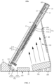
FIG. 2 is a schematic sectional view of the wireless charging device shown inFIG. 1 ; -
FIG. 3 is a schematic diagram of a wireless charging device according to another embodiment of this application; -
FIG. 4 is a schematic sectional view of the wireless charging device shown inFIG. 3 ; -
FIG. 5 is a schematic diagram of a wireless charging device according to another embodiment of this application; and -
FIG. 6 is a schematic sectional view of the wireless charging device shown inFIG. 5 . - Wireless charging device: 100, 100a, 100b; Housing: 10, 10a, 10b; Panel: 11; Support part: 12; Spacing part: 13; Air vent: 101; First cavity: 102; First segment: 1021; Second segment: 1022; Second cavity: 103; Third cavity: 104; Air intake vent: 105; Air exhaust vent: 106; Fastener: 14; Transmit coil: 20; Coil body: 21; Soft magnet: 23; Heat dissipation assembly: 30; Semiconductor refrigeration chip: 31, 31a, 31b; Cold end: 311, 311a, 311b; Hot end: 312, 312a, 312b; Fan: 32, 32a, 32b; First thermally conductive member: 33; Second thermally conductive member: 34; Third thermally conductive member: 35; Circuit board: 40; Electronic device: 200.
- To further describe technical means and effects that are used by this application to achieve a predetermined application objective, the following describes embodiments with reference to the accompanying drawings and implementations. Apparently, the described embodiments are merely some rather than all of the embodiments of this application.
- Unless otherwise defined, all technical and scientific terms used in this specification have the same meaning as those commonly understood by persons skilled in the art of this application. The terms used in the specification of this application are merely intended to describe specific embodiments, and are not intended to limit this application.
- Some implementations of this application are described in detail below with reference to the accompanying drawings. If there is no conflict, the following embodiments and features in the embodiments may be mutually combined.
- Referring to
FIG. 1 andFIG. 2 , this application provides awireless charging device 100. Thewireless charging device 100 is configured to charge anelectronic device 200. Theelectronic device 200 may be a mobile phone, a tablet personal computer (Tablet Personal Computer), a laptop computer (Laptop Computer), a personal digital assistant (Personal Digital Assistant, PDA), a mobile Internet device (Mobile Internet Device, MID), a wearable device (Wearable Device), or the like. - The
wireless charging device 100 includes ahousing 10, a transmitcoil 20, and aheat dissipation assembly 30. Afirst cavity 102 and asecond cavity 103 are disposed in thehousing 10. Thesecond cavity 103 is located above thefirst cavity 102. Thehousing 10 is provided with apanel 11. The transmitcoil 20 is disposed in thefirst cavity 102, and is in contact with one side of thepanel 11. Thewireless charging device 100 generates an alternating current electromagnetic field when the transmitcoil 20 is connected to an alternating current power supply, so that a coil in theelectronic device 200 generates an inducting voltage in the alternating current magnetic field, thereby implementing wireless charging on theelectronic device 200. - The
electronic device 200 is placed on thehousing 10, and theelectronic device 200 is at a distance from thepanel 11, as shown inFIG. 1 . Theheat dissipation assembly 30 includes asemiconductor refrigeration chip 31 and afan 32. Thesemiconductor refrigeration chip 31 and thefan 32 are separately disposed in thefirst cavity 102. Thehousing 10 is further provided with anair vent 101 communicating with thefirst cavity 102. Theair vent 101 is located under thepanel 11. Thesemiconductor refrigeration chip 31 is made based on a Peltier (Peltier) effect of a semiconductor material. The Peltier effect refers to a phenomenon that one end absorbs heat and the other end dissipates heat when a direct current passes through a galvanic couple formed by two different semiconductor materials in series. Thesemiconductor refrigeration chip 31 made based on this principle includes acold end 311 and a hot end 312 that are on opposite sides. Thecold end 311 may cool adjacent components, and heat is transferred through the hot end 312. Thesemiconductor refrigeration chip 31 is disposed on thehousing 10, and is located in thefirst cavity 102. The hot end 312 of thesemiconductor refrigeration chip 31 is fixedly connected to thehousing 10, and thecold end 311 protrudes into thefirst cavity 102. The air blown by thefan 32 passes through thecold end 311 and is blown out from theair vent 101. - A temperature of the air that passes through the
cold end 311 is reduced, and the air passes between thepanel 11 and theelectronic device 200 to reduce a temperature of theelectronic device 200. - The
panel 11 is made of an insulating and heat-insulation material (for example, a glass fiber or a vacuum plate). Heat generated by the transmitcoil 20 is not conducted between thepanel 11 and theelectronic device 200 through thepanel 11, so that cooling of theelectronic device 200 by the air blown from theair vent 101 is improved. - It may be understood that, in another embodiment, the
panel 11 may alternatively be made of an insulating and thermally conductive non-metallic material, such as a carbon fiber material or a ceramic material. The air blown from theair vent 101 may cool both thepanel 11 and theelectronic device 200, and the cooling of thepanel 11 reduces a temperature of the transmitcoil 20. - The
fan 32 and thesemiconductor refrigeration chip 31 are located in thefirst cavity 102. Thesemiconductor refrigeration chip 31 is closer to theair vent 101 than thefan 32. Anair intake vent 105 is disposed at the bottom of thehousing 10. Theair intake vent 105 is located on a side that is of thefirst cavity 102 and that is away from thesecond cavity 103. Theair intake vent 105 communicates with thefirst cavity 102. Air enters thefirst cavity 102 from theair intake vent 105, and thefan 32 guides the air to blow between theelectronic device 200 and thepanel 11 through the air vent. - It may be understood that, in another embodiment, the
air intake vent 105 may alternatively be disposed on a side that is of thefirst cavity 102 and that is away from theair vent 101. A position of theair intake vent 105 on thefirst cavity 102 may be set based on an air guiding direction of thefan 32, provided that thefan 32 can guide air entering from theair intake vent 105 to be blown out of theair vent 101. - There is one
semiconductor refrigeration chip 31 and the hot end 312 of thesemiconductor refrigeration chip 31 is disposed on a cavity wall that is of thefirst cavity 102 and that faces thesecond cavity 103, but is not limited thereto. For example, in another embodiment, there are two semiconductor refrigeration chips 31. The twosemiconductor refrigeration chips 31 are disposed opposite to each other on two opposite cavity walls of thefirst cavity 102, and cold ends 311 of the two semiconductor refrigeration chips are disposed opposite to each other. The air blown by thefan 32 is blown to the cold ends 311 of the twosemiconductor refrigeration chips 31, so that the air blown between theelectronic device 200 and thepanel 11 is quickly cooled, thereby improving efficiency of reducing a temperature of theelectronic device 200. - The
housing 10 is further provided with asupport part 12 on a side of theair vent 101. Thesupport part 12 is configured to support theelectronic device 200. Thehousing 10 is further provided with aspacing part 13. There are two spacingparts 13. The twospacing parts 13 are disposed at intervals and protrude from thepanel 11. Thespacing part 13 is configured to be in contact with theelectronic device 200, so that there is a distance between theelectronic device 200 and thepanel 11. - It may be understood that, in another embodiment, a quantity of
spacing parts 13 may be one or another number. Provided that thespacing part 13 protrudes from thepanel 11, theelectronic device 200 is placed on thehousing 10, and is in contact with thespacing part 13, so that there is a distance between theelectronic device 200 and thepanel 11. - The
first cavity 102 includes afirst segment 1021 and asecond segment 1022 that communicate with each other. Thefan 32 is disposed in thefirst segment 1021. Thesecond segment 1022 is closer to theair vent 101 than thefirst segment 1021. Thesecond segment 1022 extends upward along a curve from thefirst segment 1021 to theair vent 101, so as to guide the air blown by thefan 32 to blow out from theair vent 101, and reduce a force of the air blown by theair vent 101 on theelectronic device 200 placed on thehousing 10. Thefan 32 blows air in a direction of thefirst segment 1021 toward thesecond segment 1022. - It may be understood that, in another embodiment, the
first segment 1021 may alternatively be obliquely disposed along a straight line, or thefirst segment 1021 extends from thesecond segment 1022 to theair vent 101 along two straight paths that intersect along an L-shape or a V-shape. - The
heat dissipation assembly 30 further includes a first thermallyconductive member 33. The first thermallyconductive member 33 is disposed on thehousing 10, and is located in thefirst cavity 102. Thepanel 11, the transmitcoil 20, and the first thermallyconductive member 33 are sequentially stacked, and sequentially transmit heat. - The first thermally
conductive member 33 may be separated from thehousing 10, and the first thermallyconductive member 33 is exposed from thehousing 10 and is in contact with air outside thehousing 10. The first thermallyconductive member 33 may be in an integrated structure with thehousing 10, and the first thermallyconductive member 33 is in contact with the air outside thehousing 10. - Heat of the transmit
coil 20 is conducted to the first thermallyconductive member 33, and the first thermallyconductive member 33 dissipates the heat to the outside of thefirst cavity 102. - It may be understood that, in another embodiment, the first thermally
conductive member 33 may alternatively be omitted. - The transmit
coil 20 includes acoil body 21 and asoft magnet 23. Thepanel 11, thecoil body 21, and thesoft magnet 23 are sequentially disposed. Thesoft magnet 23 can improve strength of a magnetic field generated when thecoil body 21 is energized. - The
soft magnet 23 is made of a soft magnetic material, for example, thesoft magnet 23 may be made of a ferrite or an iron-based amorphous alloy. - The transmit
coil 20 and the first thermallyconductive member 33 may be separately connected to thehousing 10 in an adhesive manner, but is not limited thereto. For example, as shown inFIG. 2 , the first thermallyconductive member 33 is locked on thehousing 10 by using afastener 14 such as a screw, so that the first thermallyconductive member 33 and thepanel 11 are respectively pressed against both sides of the transmitcoil 20, and the transmitcoil 20 and the first thermallyconductive member 33 are fastened to thehousing 10, thereby avoiding impact of heat-conducting property of adhesive on heat conduction efficiency of the transmitcoil 20 and the first thermallyconductive member 33. - The
wireless charging device 100 further includes acircuit board 40. Thecircuit board 40 is disposed on thehousing 10, and is located in thefirst cavity 102. Thecircuit board 40 is located on a side that is of thefan 32 and that is away from theair intake vent 105, and thecircuit board 40 is electrically connected to the transmitcoil 20, thefan 32, and thesemiconductor refrigeration chip 31, so as to control the transmitcoil 20, thefan 32, and thesemiconductor refrigeration chip 31 to operate. - In the
wireless charging device 100, the air blown by thefan 32 passes through thecold end 311 of thesemiconductor refrigeration chip 31, so that the air cools down and passes through theair vent 101 to flow between thepanel 11 and theelectronic device 200, thereby improving a cooling effect of theelectronic device 200. - Referring to
FIG. 3 andFIG. 4 , a difference between awireless charging device 100a in another embodiment and thewireless charging device 100 lies in that thewireless charging device 100a further includes anotherfan 32a and anothersemiconductor refrigeration chip 31a, and a structure of ahousing 10 of thewireless charging device 100a is different from a structure of ahousing 10a of thewireless charging device 100a. - The
semiconductor refrigeration chip 31a is stacked on a side of a transmitcoil 20 and a first thermallyconductive member 33. Thefan 32a is disposed on a first housing, and is located in afirst cavity 102, but is not limited thereto. Thefan 32a is located on a side that is of thefan 32a and that is away from thesemiconductor refrigeration chip 31a. - The
housing 10a is further provided with athird cavity 104 and anair exhaust vent 106. Thethird cavity 104 communicates with both thefirst cavity 102 and asecond cavity 103. Thethird cavity 104 is located above thefirst cavity 102, and is located on a side of thesecond cavity 103. Theair exhaust vent 106 is located on a side that is of thethird cavity 104 and that is away from the first thermallyconductive member 33. The air blown by thefan 32a can be blown to the first thermallyconductive member 33 and discharged from theair exhaust vent 106, thereby reducing a temperature of the first thermallyconductive member 33, and then reducing a temperature of the transmitcoil 20. - The first thermally
conductive member 33 is obliquely disposed above thefan 32a, to increase projection of the first thermallyconductive member 33 on thefan 32a, so that the air blown by thefan 32a may be directly blown to a larger area of the first thermallyconductive member 33, thereby improving efficiency of reducing the temperature of the first thermallyconductive member 33. - The air blown by the
fan 32a and the air blown by thefan 32 respectively are respectively blown to the first thermallyconductive member 33 and between theelectronic device 200 and thepanel 11, so that both theelectronic device 200 and thewireless charging device 100 are cooled, thereby improving cooling efficiency. - The
wireless charging device 100a further includes acircuit board 40. Thecircuit board 40 is disposed on thehousing 10a, and is located on a cavity wall that is of thethird cavity 104 and that is away from the first thermallyconductive member 33. Thecircuit board 40 is electrically connected to the transmitcoil 20, thefan 32a, and thefan 32a. Thecircuit board 40 is obliquely disposed above thefan 32a, so that the air blown by thefan 32a can be blown to thecircuit board 40, and thecircuit board 40 is cooled. - The
wireless charging device 100a further includes a second thermallyconductive member 34, and the second thermallyconductive member 34 is disposed between the transmitcoil 20 and thesemiconductor refrigeration chip 31a. The second thermallyconductive member 34 is a thermally conductive structure made of a thermally conductive material that is deformable under pressure. For example, the second thermallyconductive member 34 is a sheet-like structure made of thermally conductive silicone. Hardness of the transmitcoil 20 and hardness of thesemiconductor refrigeration chip 31a are greater than hardness of the second thermallyconductive member 34. When one of surfaces of the transmitcoil 20 and thesemiconductor refrigeration chip 31a that are opposite to each other is uneven because of deformation, a pit, or a bump, the second thermallyconductive member 34 is pressed by the transmitcoil 20 and thesemiconductor refrigeration chip 31a to deform, so as to be evenly in contact with both the transmitcoil 20 and thesemiconductor refrigeration chip 31a, thereby improving heat conduction efficiency. - It may be understood that, in another embodiment, the second thermally
conductive member 34 may alternatively be made of a hard thermally conductive material. When an area of acold end 311a of thesemiconductor refrigeration chip 31a parallel to thepanel 11 is smaller than an area of the second thermallyconductive member 34 parallel to thepanel 11, the second thermallyconductive member 34 can conduct all heat of the transmitcoil 20 parallel to thepanel 11, and then conduct the heat to thesemiconductor refrigeration chip 31a, thereby improving cooling efficiency. - It may be understood that, in another embodiment, when an area of the
cold end 311a and thehot end 312a that are of thesemiconductor refrigeration chip 31a parallel to thepanel 11 is more than 50% of an area of the transmitcoil 20 parallel to thepanel 11, both the first thermallyconductive member 33 and the second thermallyconductive member 34 may be omitted. - The
heat dissipation assembly 30 further includes a third thermallyconductive member 35, and the third thermallyconductive member 35 is disposed between thesemiconductor refrigeration chip 31a and the first thermallyconductive member 33. The third thermallyconductive member 35 is a thermally conductive structure made of a thermally conductive material that is deformable under pressure. The third thermallyconductive member 35 is pressed by the first thermallyconductive member 33 and thesemiconductor refrigeration chip 31a to deform, so as to be evenly in contact with both the first thermallyconductive member 33 and thesemiconductor refrigeration chip 31a, thereby improving heat conduction efficiency. - It may be understood that, in another embodiment, the
semiconductor refrigeration chip 31a may alternatively be omitted. Heat of the transmitcoil 20 is conducted to the first thermallyconductive member 33, and thefan 32a blows air to the first thermallyconductive member 33, which can also reduce a temperature of the first thermallyconductive member 33. - In the
wireless charging device 100a, the air blown by thefan 32 passes through thecold end 311 of thesemiconductor refrigeration chip 31, so that the air cools down and passes through theair vent 101 to flow between thepanel 11 and theelectronic device 200, thereby improving a cooling effect of theelectronic device 200. In thewireless charging device 100a, the air is blown to the first thermallyconductive member 33 through thefan 32a, a temperature of the transmitcoil 20 is reduced through heat conduction between the first thermallyconductive member 33 and the transmitcoil 20. Thewireless charging device 100a can cool both theelectronic device 200 and the transmitcoil 20. - Referring to
FIG. 5 andFIG. 6 , in still another embodiment, awireless charging device 100b includes a housing 10ab, a transmitcoil 20, and aheat dissipation assembly 30. The housing 10ab is provided with apanel 11. Theheat dissipation assembly 30 includes asemiconductor refrigeration chip 31b, a first thermallyconductive member 33, and afan 32b. Thesemiconductor refrigeration chip 31b includes acold end 311b and ahot end 312b. Thepanel 11, the transmitcoil 20, thesemiconductor refrigeration chip 31b, and the first thermallyconductive member 33 are sequentially stacked. Thecold end 311b faces the transmitcoil 20. Thehot end 312b faces the first thermallyconductive member 33. Thefan 32b is disposed in the housing 10ab. The first thermallyconductive member 33 is obliquely disposed above thefan 32b, to increase projection of the first thermallyconductive member 33 on thefan 32b, so that the air blown by thefan 32b may be directly blown to a larger area of the first thermallyconductive member 33, thereby improving efficiency of reducing a temperature of the first thermallyconductive member 33. - The
panel 11 is made of an insulating and thermally conductive non-metallic material, such as a carbon fiber material or a ceramic material. - The housing 10ab is further provided with a
support part 12 located under thepanel 11. Thesupport part 12 is configured to support theelectronic device 200, so that theelectronic device 200 is placed on the housing 10ab, and is in contact with thepanel 11. - The air blown by the
fan 32b reduces a temperature of the first thermallyconductive member 33, to improve a cooling effect of thecold end 311b of thesemiconductor refrigeration chip 31b that is in contact with the first thermallyconductive member 33, and then reduce temperatures of the transmitcoil 20 and thepanel 11 that are sequentially in contact with thecold end 311b, thereby reducing a temperature of theelectronic device 200 that is in contact with thepanel 11. - A
first cavity 102, asecond cavity 103, and athird cavity 104 are disposed in the housing 10ab. Thesecond cavity 103 is located above thefirst cavity 102. Thefan 32b is located in thefirst cavity 102. The transmitcoil 20, thesemiconductor refrigeration chip 31b, and the first thermallyconductive member 33 are sequentially disposed in thesecond cavity 103. The housing 10ab is further provided with anair exhaust vent 106, and theair exhaust vent 106 communicates with thethird cavity 104. Anair intake vent 105 communicating with thefirst cavity 102 is disposed at the bottom of the housing 10ab. Thethird cavity 104 communicates with both thefirst cavity 102 and asecond cavity 103. - The
third cavity 104 is located above thefirst cavity 102, and is located on a side of thesecond cavity 103, to enable the air blown by thefan 32b to enter thethird cavity 104 from thefirst cavity 102 and be directly blown to the first thermallyconductive member 33, so as to effectively reduce a temperature of thehot end 312b of thesemiconductor refrigeration chip 31b, so that a temperature of thecold end 311b of thesemiconductor refrigeration chip 31b is maintained at a lower temperature, or a low-temperature state is maintained for a longer time. Air enters thefirst cavity 102 from theair intake vent 105, is blown out from thefan 32b and is blown to the first thermallyconductive member 33, and then is discharged from theair exhaust vent 106. - The
wireless charging device 100b further includes acircuit board 40. Thecircuit board 40 is disposed on the housing 10ab, and is located in thethird cavity 104. Thecircuit board 40 is electrically connected to the transmitcoil 20 and thefan 32b. Thecircuit board 40 is obliquely disposed above thefan 32b, so that the air blown by thefan 32b can be blown to thecircuit board 40, and thecircuit board 40 is cooled. - The
wireless charging device 100b further includes a second thermallyconductive member 34, and the second thermallyconductive member 34 is disposed between the transmitcoil 20 and thesemiconductor refrigeration chip 31b. The second thermallyconductive member 34 is a thermally conductive structure made of a thermally conductive material that is deformable under pressure. For example, the second thermallyconductive member 34 is a sheet-like structure made of thermally conductive silicone. Hardness of the transmitcoil 20 and hardness of thesemiconductor refrigeration chip 31b are greater than hardness of the second thermallyconductive member 34. When one of surfaces of the transmit coil 20and thesemiconductor refrigeration chip 31a that are opposite to each other is uneven because of deformation, a pit, or a bump, the second thermallyconductive member 34 is pressed by the transmitcoil 20 and thesemiconductor refrigeration chip 31b to deform, so as to be evenly in contact with both the transmitcoil 20 and thesemiconductor refrigeration chip 31b, thereby improving heat conductive efficiency. - It may be understood that, in another embodiment, the second thermally
conductive member 34 may alternatively be made of a hard thermally conductive material. When an area of thecold end 311b of thesemiconductor refrigeration chip 31b parallel to thepanel 11 is smaller than an area of the second thermallyconductive member 34 parallel to thepanel 11, the second thermallyconductive member 34 can conduct all heat of the transmitcoil 20 parallel to thepanel 11, and then conduct the heat to thesemiconductor refrigeration chip 31b, thereby improving cooling efficiency. - It may be understood that, in another embodiment, when an area of the
cold end 311b and thehot end 312b that are of thesemiconductor refrigeration chip 31b parallel to thepanel 11 is more than 50% of an area of the transmitcoil 20 parallel to thepanel 11, both the first thermallyconductive member 33 and the second thermallyconductive member 34 may be omitted. - The
heat dissipation assembly 30 further includes a third thermallyconductive member 35, and the third thermallyconductive member 35 is disposed between thesemiconductor refrigeration chip 31b and the first thermallyconductive member 33. When an area of thehot end 312b of thesemiconductor refrigeration chip 31b parallel to thepanel 11 is smaller than an area of the third thermallyconductive member 35 parallel to thepanel 11, the third thermallyconductive member 35 can conduct all heat of thehot end 312b parallel to thepanel 11, and then conduct the heat to the first thermallyconductive member 33, thereby improving cooling efficiency. - The third thermally
conductive member 35 is a thermally conductive structure made of a thermally conductive material that is deformable under pressure. The third thermallyconductive member 35 is pressed by the first thermallyconductive member 33 and thesemiconductor refrigeration chip 31b to deform, so as to be evenly in contact with both the first thermallyconductive member 33 and thesemiconductor refrigeration chip 31b, thereby improving heat conductive efficiency. - The
wireless charging device 100b cools the transmitcoil 20, thepanel 11, and theelectronic device 200 that are sequentially in contact with each other through thecold end 311b of thesemiconductor refrigeration chip 31b, and thefan 32b blows air to the first thermallyconductive member 33, so that thehot end 312b that is in contact with the first thermallyconductive member 33 is cooled, thereby improving a cooling effect. - The
wireless charging device 100, thewireless charging device 100a, and thewireless charging device 100b may charge the electronic device, and a heat dissipation effect is good in a charging process. For example, the electronic device is a mobile phone, a tablet computer, a headset, a headset case, or a smartwatch. - The foregoing embodiments are merely intended to describe the technical solutions of this application, but are not intended to constitute limitations. Although this application is described in detail with reference to preferred embodiments, persons of ordinary skill in the art should understand that the technical solutions of this application may be modified or equivalent replaced without departing from the spirit and essence of the technical solutions of this application.
Claims (13)
- A wireless charging device, comprising a housing, a transmit coil, and a heat dissipation assembly, wherein the housing is provided with a panel, and the transmit coil is disposed in the housing, and is located on a side of the panel;the housing is configured to place an electronic device to be charged, and make the electronic device have a distance from the panel; and the housing is provided with an air vent located under the panel; andthe heat dissipation assembly comprises:a semiconductor refrigeration chip, comprising a cold end and a hot end, wherein the hot end is disposed on the housing; anda fan, disposed in the housing, and air blown by the fan passes through the cold end and is blown out from the air vent.
- The wireless charging device according to claim 1, wherein the heat dissipation assembly further comprises another fan and a first thermally conductive member, the first thermally conductive member is disposed on a side that is of the transmit coil and that is away from the panel, the another fan is disposed on the housing, and the another fan blows air to the first thermally conductive member.
- The wireless charging device according to claim 2, wherein the first thermally conductive member is obliquely disposed above the another fan, and the another fan blows air from an upper side.
- The wireless charging device according to claim 2, wherein the heat dissipation assembly further comprises another semiconductor refrigeration chip, the another semiconductor refrigeration chip is disposed between the transmit coil and the first thermally conductive member, the cold end faces the transmit coil, and the hot end faces the first thermally conductive member.
- The wireless charging device according to claim 2, wherein a first cavity and a second cavity are disposed in the housing, and the second cavity is located above the first cavity;the fan and the another fan are disposed in the first cavity; andthe transmit coil, the semiconductor refrigeration chip, and the first thermally conductive member are sequentially disposed in the second cavity.
- The wireless charging device according to claim 5, wherein the first cavity comprises a first segment and a second segment, the second segment extends upward along a curve from the first segment to the air vent, the fan is located in the first segment, and the semiconductor refrigeration chip is located in the second segment.
- The wireless charging device according to claim 5, wherein the wireless charging device further comprises a circuit board, the housing is further provided with a third cavity and an air exhaust vent that communicate with each other, and the third cavity communicates with both the first cavity and the second cavity; and the third cavity is located above the first cavity, and is located on a side of the second cavity; and
the circuit board is electrically connected to the transmit coil, the fan, and the another fan, the circuit board is disposed on the housing, and is located in the third cavity, and air blown by the another fan can be blown to the first thermally conductive member and the circuit board, and is discharged from the air exhaust vent. - A wireless charging device, comprising a housing, a transmit coil, and a heat dissipation assembly, wherein the housing is provided with a panel, and the heat dissipation assembly comprises:a semiconductor refrigeration chip, comprising a cold end and a hot end;a first thermally conductive member, wherein the panel, the transmit coil, the semiconductor refrigeration chip, and the first thermally conductive member are sequentially stacked, the cold end faces the transmit coil, and the hot end faces the first thermally conductive member; anda fan, disposed in the housing, wherein the first thermally conductive member is obliquely disposed above the fan.
- The wireless charging device according to claim 8, wherein a first cavity and a second cavity are disposed in the housing, and the second cavity is located above the first cavity;the fan is located in the first cavity; andthe transmit coil, the semiconductor refrigeration chip, and the first thermally conductive member are sequentially disposed in the second cavity.
- The wireless charging device according to claim 9, wherein the wireless charging device further comprises a circuit board, the housing is further provided with a third cavity and an air exhaust vent that communicate with each other, and the third cavity communicates with both the first cavity and the second cavity; and the third cavity is located above the first cavity, and is located on a side of the second cavity; and
the circuit board is electrically connected to the transmit coil and the fan, the circuit board is disposed on the housing, and is located in the third cavity, and air blown by the fan can be blown to the first thermally conductive member and the circuit board, and is discharged from the air exhaust vent. - The wireless charging device according to any one of claims 2 to 10, wherein the wireless charging device further comprises a second thermally conductive member, and the second thermally conductive member is disposed between the transmit coil and the semiconductor refrigeration chip.
- The wireless charging device according to claim 11, wherein the heat dissipation assembly further comprises a third thermally conductive member, and the third thermally conductive member is disposed between the semiconductor refrigeration chip and the first thermally conductive member.
- The wireless charging device according to claim 12, wherein the second thermally conductive member or the third thermally conductive member is a thermally conductive structure made of a thermally conductive material that is deformable under pressure.
Applications Claiming Priority (2)
| Application Number | Priority Date | Filing Date | Title |
|---|---|---|---|
| CN202123159198.2U CN217159308U (en) | 2021-12-14 | 2021-12-14 | Wireless charging equipment |
| PCT/CN2022/114626 WO2023109176A1 (en) | 2021-12-14 | 2022-08-24 | Wireless charging apparatus |
Publications (3)
| Publication Number | Publication Date |
|---|---|
| EP4224666A1 true EP4224666A1 (en) | 2023-08-09 |
| EP4224666A4 EP4224666A4 (en) | 2024-07-31 |
| EP4224666B1 EP4224666B1 (en) | 2026-05-06 |
Family
ID=82684295
Family Applications (1)
| Application Number | Title | Priority Date | Filing Date |
|---|---|---|---|
| EP22862331.0A Active EP4224666B1 (en) | 2021-12-14 | 2022-08-24 | Wireless charging apparatus |
Country Status (4)
| Country | Link |
|---|---|
| US (1) | US20240222987A1 (en) |
| EP (1) | EP4224666B1 (en) |
| CN (1) | CN217159308U (en) |
| WO (1) | WO2023109176A1 (en) |
Cited By (1)
| Publication number | Priority date | Publication date | Assignee | Title |
|---|---|---|---|---|
| US20220217866A1 (en) * | 2019-11-05 | 2022-07-07 | Huawei Digital Power Technologies Co., Ltd. | Wireless charging base |
Families Citing this family (5)
| Publication number | Priority date | Publication date | Assignee | Title |
|---|---|---|---|---|
| CN217159308U (en) * | 2021-12-14 | 2022-08-09 | 荣耀终端有限公司 | Wireless charging equipment |
| CN219627381U (en) * | 2022-12-16 | 2023-09-01 | 惠州市华阳多媒体电子有限公司 | High-power wireless charger and vehicle-mounted charging structure |
| CN117955258B (en) * | 2024-03-26 | 2024-08-30 | 荣耀终端有限公司 | Wireless charging device and wireless charging control method |
| USD1081562S1 (en) * | 2025-01-18 | 2025-07-01 | Yifeng Intelligent (Shenzhen) Co., Ltd. | Wireless charger |
| USD1090432S1 (en) * | 2025-02-21 | 2025-08-26 | Lei Lv | Wireless charger |
Family Cites Families (9)
| Publication number | Priority date | Publication date | Assignee | Title |
|---|---|---|---|---|
| CN208707367U (en) * | 2018-09-30 | 2019-04-05 | 深圳市誉品智能光电科技有限公司 | Wireless charger |
| CN208738898U (en) * | 2018-09-30 | 2019-04-12 | 深圳市誉品智能光电科技有限公司 | Wireless charger |
| CN211744148U (en) * | 2019-11-05 | 2020-10-23 | 华为技术有限公司 | A wireless charging base |
| CN110932415B (en) * | 2019-12-19 | 2023-08-22 | 昆山联滔电子有限公司 | Wireless charger |
| US11689035B2 (en) * | 2020-01-14 | 2023-06-27 | Guangdong Oppo Mobile Telecommunications Corp., Ltd. | Wireless charger with fan |
| CN211859633U (en) * | 2020-03-10 | 2020-11-03 | 华为技术有限公司 | Wireless charging base |
| CN212543377U (en) * | 2020-03-19 | 2021-02-12 | 华为技术有限公司 | Wireless charger |
| CN113270922A (en) * | 2021-06-09 | 2021-08-17 | 维沃移动通信有限公司 | Wireless charging equipment |
| CN217159308U (en) * | 2021-12-14 | 2022-08-09 | 荣耀终端有限公司 | Wireless charging equipment |
-
2021
- 2021-12-14 CN CN202123159198.2U patent/CN217159308U/en active Active
-
2022
- 2022-08-24 US US18/025,160 patent/US20240222987A1/en active Pending
- 2022-08-24 EP EP22862331.0A patent/EP4224666B1/en active Active
- 2022-08-24 WO PCT/CN2022/114626 patent/WO2023109176A1/en not_active Ceased
Cited By (2)
| Publication number | Priority date | Publication date | Assignee | Title |
|---|---|---|---|---|
| US20220217866A1 (en) * | 2019-11-05 | 2022-07-07 | Huawei Digital Power Technologies Co., Ltd. | Wireless charging base |
| US11991854B2 (en) * | 2019-11-05 | 2024-05-21 | Huawei Digital Power Technologies Co., Ltd. | Wireless charging base |
Also Published As
| Publication number | Publication date |
|---|---|
| EP4224666B1 (en) | 2026-05-06 |
| CN217159308U (en) | 2022-08-09 |
| WO2023109176A1 (en) | 2023-06-22 |
| US20240222987A1 (en) | 2024-07-04 |
| EP4224666A4 (en) | 2024-07-31 |
Similar Documents
| Publication | Publication Date | Title |
|---|---|---|
| US20240222987A1 (en) | Wireless charging device | |
| US12046912B2 (en) | Wireless charger | |
| CN208401601U (en) | Wireless charger | |
| US6415612B1 (en) | Method and apparatus for external cooling an electronic component of a mobile hardware product, particularly a notebook computer, at a docking station having a thermoelectric cooler | |
| WO2021169807A1 (en) | Electronic device, and control method and heat dissipation system therefor | |
| US6646874B2 (en) | Mobile computer system with detachable thermoelectric module for enhanced cooling capability in a docking station | |
| CN112383153A (en) | Wireless charger with cooling device | |
| JP2001282396A (en) | Power generating mechanism and computer device and electronic equipment | |
| CN108711917A (en) | Wireless charger | |
| US20100266885A1 (en) | Battery cooling apparatus | |
| CN112714601A (en) | Heat dissipation structure for intelligent terminal and intelligent terminal | |
| CN208638058U (en) | Wireless charger | |
| CN113852144A (en) | wireless charging device | |
| CN109579353B (en) | A semiconductor refrigerator | |
| JP2908418B1 (en) | Portable information processing device | |
| US7548427B2 (en) | Apparatus and docking station for cooling of computing devices | |
| CN112928791A (en) | High-efficient heat dissipation wireless charger | |
| JP2006005081A (en) | Power component cooling system | |
| CN211859633U (en) | Wireless charging base | |
| CN213754110U (en) | Wireless charger with cooling device | |
| CN218550265U (en) | Circuit board heat dissipation device and electronic equipment | |
| CN108988436A (en) | A kind of wireless charging device and control method | |
| CN210074809U (en) | Heat dissipation seat and wireless charging device | |
| CN223206893U (en) | A wireless charging component with dual cooling | |
| CN223967698U (en) | Magnetic attraction wireless charger |
Legal Events
| Date | Code | Title | Description |
|---|---|---|---|
| STAA | Information on the status of an ep patent application or granted ep patent |
Free format text: STATUS: UNKNOWN |
|
| STAA | Information on the status of an ep patent application or granted ep patent |
Free format text: STATUS: THE INTERNATIONAL PUBLICATION HAS BEEN MADE |
|
| PUAI | Public reference made under article 153(3) epc to a published international application that has entered the european phase |
Free format text: ORIGINAL CODE: 0009012 |
|
| STAA | Information on the status of an ep patent application or granted ep patent |
Free format text: STATUS: REQUEST FOR EXAMINATION WAS MADE |
|
| 17P | Request for examination filed |
Effective date: 20230307 |
|
| AK | Designated contracting states |
Kind code of ref document: A1 Designated state(s): AL AT BE BG CH CY CZ DE DK EE ES FI FR GB GR HR HU IE IS IT LI LT LU LV MC MK MT NL NO PL PT RO RS SE SI SK SM TR |
|
| A4 | Supplementary search report drawn up and despatched |
Effective date: 20240702 |
|
| RIC1 | Information provided on ipc code assigned before grant |
Ipc: H02J 7/00 20060101AFI20240626BHEP |
|
| STAA | Information on the status of an ep patent application or granted ep patent |
Free format text: STATUS: EXAMINATION IS IN PROGRESS |
|
| 17Q | First examination report despatched |
Effective date: 20250103 |
|
| DAV | Request for validation of the european patent (deleted) | ||
| DAX | Request for extension of the european patent (deleted) | ||
| GRAP | Despatch of communication of intention to grant a patent |
Free format text: ORIGINAL CODE: EPIDOSNIGR1 |
|
| STAA | Information on the status of an ep patent application or granted ep patent |
Free format text: STATUS: GRANT OF PATENT IS INTENDED |
|
| INTG | Intention to grant announced |
Effective date: 20251204 |
|
| GRAS | Grant fee paid |
Free format text: ORIGINAL CODE: EPIDOSNIGR3 |
|
| GRAA | (expected) grant |
Free format text: ORIGINAL CODE: 0009210 |
|
| STAA | Information on the status of an ep patent application or granted ep patent |
Free format text: STATUS: THE PATENT HAS BEEN GRANTED |
|
| AK | Designated contracting states |
Kind code of ref document: B1 Designated state(s): AL AT BE BG CH CY CZ DE DK EE ES FI FR GB GR HR HU IE IS IT LI LT LU LV MC MK MT NL NO PL PT RO RS SE SI SK SM TR |
|
| REG | Reference to a national code |
Ref country code: CH Ref legal event code: F10 Free format text: ST27 STATUS EVENT CODE: U-0-0-F10-F00 (AS PROVIDED BY THE NATIONAL OFFICE) Effective date: 20260506 Ref country code: GB Ref legal event code: FG4D |