EP4224519A1 - Wiring base and electronic device - Google Patents
Wiring base and electronic device Download PDFInfo
- Publication number
- EP4224519A1 EP4224519A1 EP21875557.7A EP21875557A EP4224519A1 EP 4224519 A1 EP4224519 A1 EP 4224519A1 EP 21875557 A EP21875557 A EP 21875557A EP 4224519 A1 EP4224519 A1 EP 4224519A1
- Authority
- EP
- European Patent Office
- Prior art keywords
- openings
- region
- conductors
- ground conductor
- conductor
- Prior art date
- Legal status (The legal status is an assumption and is not a legal conclusion. Google has not performed a legal analysis and makes no representation as to the accuracy of the status listed.)
- Pending
Links
Images





Classifications
-
- H—ELECTRICITY
- H10—SEMICONDUCTOR DEVICES; ELECTRIC SOLID-STATE DEVICES NOT OTHERWISE PROVIDED FOR
- H10W—GENERIC PACKAGES, INTERCONNECTIONS, CONNECTORS OR OTHER CONSTRUCTIONAL DETAILS OF DEVICES COVERED BY CLASS H10
- H10W44/00—Electrical arrangements for controlling or matching impedance
- H10W44/20—Electrical arrangements for controlling or matching impedance at high-frequency [HF] or radio frequency [RF]
-
- H—ELECTRICITY
- H05—ELECTRIC TECHNIQUES NOT OTHERWISE PROVIDED FOR
- H05K—PRINTED CIRCUITS; CASINGS OR CONSTRUCTIONAL DETAILS OF ELECTRIC APPARATUS; MANUFACTURE OF ASSEMBLAGES OF ELECTRICAL COMPONENTS
- H05K1/00—Printed circuits
- H05K1/02—Details
- H05K1/0213—Electrical arrangements not otherwise provided for
- H05K1/0216—Reduction of cross-talk, noise or electromagnetic interference
- H05K1/0218—Reduction of cross-talk, noise or electromagnetic interference by printed shielding conductors, ground planes or power plane
- H05K1/0219—Printed shielding conductors for shielding around or between signal conductors, e.g. coplanar or coaxial printed shielding conductors
-
- H—ELECTRICITY
- H01—ELECTRIC ELEMENTS
- H01P—WAVEGUIDES; RESONATORS, LINES, OR OTHER DEVICES OF THE WAVEGUIDE TYPE
- H01P3/00—Waveguides; Transmission lines of the waveguide type
- H01P3/003—Coplanar lines
- H01P3/006—Conductor backed coplanar waveguides
-
- H—ELECTRICITY
- H01—ELECTRIC ELEMENTS
- H01P—WAVEGUIDES; RESONATORS, LINES, OR OTHER DEVICES OF THE WAVEGUIDE TYPE
- H01P3/00—Waveguides; Transmission lines of the waveguide type
- H01P3/02—Waveguides; Transmission lines of the waveguide type with two longitudinal conductors
- H01P3/026—Coplanar striplines [CPS]
-
- H—ELECTRICITY
- H01—ELECTRIC ELEMENTS
- H01P—WAVEGUIDES; RESONATORS, LINES, OR OTHER DEVICES OF THE WAVEGUIDE TYPE
- H01P3/00—Waveguides; Transmission lines of the waveguide type
- H01P3/02—Waveguides; Transmission lines of the waveguide type with two longitudinal conductors
- H01P3/08—Microstrips; Strip lines
- H01P3/081—Microstriplines
-
- H—ELECTRICITY
- H05—ELECTRIC TECHNIQUES NOT OTHERWISE PROVIDED FOR
- H05K—PRINTED CIRCUITS; CASINGS OR CONSTRUCTIONAL DETAILS OF ELECTRIC APPARATUS; MANUFACTURE OF ASSEMBLAGES OF ELECTRICAL COMPONENTS
- H05K1/00—Printed circuits
- H05K1/02—Details
- H05K1/0213—Electrical arrangements not otherwise provided for
- H05K1/0237—High frequency adaptations
- H05K1/025—Impedance arrangements, e.g. impedance matching, reduction of parasitic impedance
- H05K1/0253—Impedance adaptations of transmission lines by special lay-out of power planes, e.g. providing openings
-
- H—ELECTRICITY
- H10—SEMICONDUCTOR DEVICES; ELECTRIC SOLID-STATE DEVICES NOT OTHERWISE PROVIDED FOR
- H10W—GENERIC PACKAGES, INTERCONNECTIONS, CONNECTORS OR OTHER CONSTRUCTIONAL DETAILS OF DEVICES COVERED BY CLASS H10
- H10W76/00—Containers; Fillings or auxiliary members therefor; Seals
- H10W76/10—Containers or parts thereof
- H10W76/12—Containers or parts thereof characterised by their shape
- H10W76/15—Containers comprising an insulating or insulated base
- H10W76/157—Containers comprising an insulating or insulated base having interconnections parallel to the insulating or insulated base
-
- H—ELECTRICITY
- H05—ELECTRIC TECHNIQUES NOT OTHERWISE PROVIDED FOR
- H05K—PRINTED CIRCUITS; CASINGS OR CONSTRUCTIONAL DETAILS OF ELECTRIC APPARATUS; MANUFACTURE OF ASSEMBLAGES OF ELECTRICAL COMPONENTS
- H05K1/00—Printed circuits
- H05K1/02—Details
- H05K1/11—Printed elements for providing electric connections to or between printed circuits
- H05K1/117—Pads along the edge of rigid circuit boards, e.g. for pluggable connectors
-
- H—ELECTRICITY
- H05—ELECTRIC TECHNIQUES NOT OTHERWISE PROVIDED FOR
- H05K—PRINTED CIRCUITS; CASINGS OR CONSTRUCTIONAL DETAILS OF ELECTRIC APPARATUS; MANUFACTURE OF ASSEMBLAGES OF ELECTRICAL COMPONENTS
- H05K2201/00—Indexing scheme relating to printed circuits covered by H05K1/00
- H05K2201/09—Shape and layout
- H05K2201/09209—Shape and layout details of conductors
- H05K2201/09218—Conductive traces
- H05K2201/09227—Layout details of a plurality of traces, e.g. escape layout for Ball Grid Array [BGA] mounting
-
- H—ELECTRICITY
- H05—ELECTRIC TECHNIQUES NOT OTHERWISE PROVIDED FOR
- H05K—PRINTED CIRCUITS; CASINGS OR CONSTRUCTIONAL DETAILS OF ELECTRIC APPARATUS; MANUFACTURE OF ASSEMBLAGES OF ELECTRICAL COMPONENTS
- H05K2201/00—Indexing scheme relating to printed circuits covered by H05K1/00
- H05K2201/09—Shape and layout
- H05K2201/09209—Shape and layout details of conductors
- H05K2201/095—Conductive through-holes or vias
- H05K2201/09609—Via grid, i.e. two-dimensional array of vias or holes in a single plane
-
- H—ELECTRICITY
- H05—ELECTRIC TECHNIQUES NOT OTHERWISE PROVIDED FOR
- H05K—PRINTED CIRCUITS; CASINGS OR CONSTRUCTIONAL DETAILS OF ELECTRIC APPARATUS; MANUFACTURE OF ASSEMBLAGES OF ELECTRICAL COMPONENTS
- H05K2201/00—Indexing scheme relating to printed circuits covered by H05K1/00
- H05K2201/09—Shape and layout
- H05K2201/09209—Shape and layout details of conductors
- H05K2201/09654—Shape and layout details of conductors covering at least two types of conductors provided for in H05K2201/09218 - H05K2201/095
- H05K2201/09672—Superposed layout, i.e. in different planes
-
- H—ELECTRICITY
- H05—ELECTRIC TECHNIQUES NOT OTHERWISE PROVIDED FOR
- H05K—PRINTED CIRCUITS; CASINGS OR CONSTRUCTIONAL DETAILS OF ELECTRIC APPARATUS; MANUFACTURE OF ASSEMBLAGES OF ELECTRICAL COMPONENTS
- H05K2201/00—Indexing scheme relating to printed circuits covered by H05K1/00
- H05K2201/09—Shape and layout
- H05K2201/09209—Shape and layout details of conductors
- H05K2201/09654—Shape and layout details of conductors covering at least two types of conductors provided for in H05K2201/09218 - H05K2201/095
- H05K2201/09681—Mesh conductors, e.g. as a ground plane
-
- H—ELECTRICITY
- H05—ELECTRIC TECHNIQUES NOT OTHERWISE PROVIDED FOR
- H05K—PRINTED CIRCUITS; CASINGS OR CONSTRUCTIONAL DETAILS OF ELECTRIC APPARATUS; MANUFACTURE OF ASSEMBLAGES OF ELECTRICAL COMPONENTS
- H05K2201/00—Indexing scheme relating to printed circuits covered by H05K1/00
- H05K2201/09—Shape and layout
- H05K2201/09209—Shape and layout details of conductors
- H05K2201/09654—Shape and layout details of conductors covering at least two types of conductors provided for in H05K2201/09218 - H05K2201/095
- H05K2201/0969—Apertured conductors
-
- H—ELECTRICITY
- H10—SEMICONDUCTOR DEVICES; ELECTRIC SOLID-STATE DEVICES NOT OTHERWISE PROVIDED FOR
- H10W—GENERIC PACKAGES, INTERCONNECTIONS, CONNECTORS OR OTHER CONSTRUCTIONAL DETAILS OF DEVICES COVERED BY CLASS H10
- H10W44/00—Electrical arrangements for controlling or matching impedance
- H10W44/20—Electrical arrangements for controlling or matching impedance at high-frequency [HF] or radio frequency [RF]
- H10W44/226—Electrical arrangements for controlling or matching impedance at high-frequency [HF] or radio frequency [RF] for HF amplifiers
- H10W44/234—Arrangements for impedance matching
-
- H—ELECTRICITY
- H10—SEMICONDUCTOR DEVICES; ELECTRIC SOLID-STATE DEVICES NOT OTHERWISE PROVIDED FOR
- H10W—GENERIC PACKAGES, INTERCONNECTIONS, CONNECTORS OR OTHER CONSTRUCTIONAL DETAILS OF DEVICES COVERED BY CLASS H10
- H10W44/00—Electrical arrangements for controlling or matching impedance
- H10W44/20—Electrical arrangements for controlling or matching impedance at high-frequency [HF] or radio frequency [RF]
- H10W44/259—Optical signal interface
-
- H—ELECTRICITY
- H10—SEMICONDUCTOR DEVICES; ELECTRIC SOLID-STATE DEVICES NOT OTHERWISE PROVIDED FOR
- H10W—GENERIC PACKAGES, INTERCONNECTIONS, CONNECTORS OR OTHER CONSTRUCTIONAL DETAILS OF DEVICES COVERED BY CLASS H10
- H10W70/00—Package substrates; Interposers; Redistribution layers [RDL]
- H10W70/60—Insulating or insulated package substrates; Interposers; Redistribution layers
- H10W70/62—Insulating or insulated package substrates; Interposers; Redistribution layers characterised by their interconnections
- H10W70/65—Shapes or dispositions of interconnections
Definitions
- the present disclosure relates to a wiring base and an electronic device.
- a known wiring base (for example, a package) includes an electronic component mounted therein and provides electrical connection between the electronic component and an external wiring line.
- the wiring base may include a main body containing the electronic component and a terminal member extending out of the main body.
- the terminal member includes a signal conductor and a ground conductor that are electrically connected to the electronic component.
- a wiring line of the external board is electrically connected to the electronic component.
- a known terminal member includes a signal line (microstrip line) that enables transmission of a high-frequency signal.
- the signal line includes a signal conductor and a ground conductor facing the signal conductor across an insulator.
- International Publication No. 2010/103722 describes a technology for adjusting the impedance of the signal line by forming openings in a mesh pattern in the ground conductor of the terminal member.
- a wiring base includes a base, a signal conductor, and a ground conductor including a first ground conductor.
- the base includes a first surface, a first region, and a second region.
- the first region is located near an outer side of the first surface.
- An external board is mounted in the first region.
- the second region is other than the first region.
- the signal conductor extends through a region including the first region of the first surface in a first direction away from the outer side.
- the first ground conductor is located in the base at a distance from the signal conductor of less than 1/4 of a wavelength of a high-frequency signal in a direction perpendicular to the first surface. The high-frequency signal is transmitted through the signal conductor.
- the first ground conductor includes a first grid portion at a first location overlapping the first region and at least a portion of the signal conductor in a see-through plan view viewed in a direction toward the first surface.
- the first grid portion includes a segment disposed between first openings. Lengths of the first openings in the first direction and a second direction crossing the first direction are 1/8 or more and 1/4 or less of the wavelength of the high-frequency signal.
- a through conductor is located on the first grid portion.
- an electronic device includes the above-described wiring base and an electronic component connected to the wiring base.
- a wiring base 100 and an electronic device 1 may include any components that are not illustrated in the drawings referred to below. Dimensions of components illustrated in the drawings do not accurately reflect the actual dimensions and dimensional ratios of the components.
- the structure of the electronic device 1 according to a first embodiment will be described with reference to FIGs. 1 and 2 .
- the electronic device 1 includes the wiring base 100 and an electronic component 200.
- the electronic device 1 also includes a lid body 30 sealing the wiring base 100.
- the wiring base 100 includes a main body 20 and a terminal member 10.
- the terminal member 10 extends out of the main body 20.
- the lid body 30 may be regarded as sealing the main body 20.
- the wiring base 100 is an electronic device package including the main body 20 in which the electronic component 200 is mounted.
- the electronic device package provides electrical connection between the electronic component 200 and wiring lines of an external board 2 through the terminal member 10.
- the wiring base 100 holds, for example, the electronic component 200 for optical communication.
- the electronic component 200 may receive or output a high-frequency signal for optical communication (for example, the modulation rate is about 96 Gbaud or less and the frequency band is about 75 GHz or less).
- the electronic component 200 may be a light emitting element or a light receiving element. These are examples, and the electronic component 200 to be mounted is not limited to the above-described elements.
- the main body 20 includes a bottom portion 21, a frame 22, and a seal member 23.
- the bottom portion 21 is a rectangular plate-shaped member.
- directions parallel to the sides of the rectangular bottom portion 21 are referred to as an X direction and a Y direction, and a direction perpendicular to the bottom portion 21 and extending from the bottom portion 21 toward the lid body 30 is referred to as a Z direction.
- a surface facing in the +Z direction is referred to as an "upper surface”
- a surface facing in the -Z direction is referred to as a "lower surface”.
- a layer located in the -Z direction relative to another object is referred to as a layer "below” the object.
- a view in the Z direction is referred to as a "plan view”
- a see-through view seen through other components in the Z direction is referred to as a "see-through plan view”.
- An upper surface of the bottom portion 21 includes a placement region in which the electronic component 200 is placed.
- the electronic component 200 placed in the placement region includes terminals electrically connected to wiring lines formed on the upper surface of the bottom portion 21.
- the frame 22 is a frame-shaped member surrounding the placement region for the electronic component 200 in plan view.
- the frame 22 extends in the +Z direction from an outer peripheral portion of the bottom portion 21 to form a frame-shaped side wall.
- the frame 22 may include through holes 22a for allowing optical fibers or the like to extend therethrough.
- Each of the bottom portion 21 and the frame 22 may, for example, include a plurality of insulative boards stacked in the Z direction.
- Each insulative board may be, for example, a ceramic sintered body, such as an aluminum-oxide-based sintered body, an aluminum-nitride-based sintered body, a silicon-carbide-based sintered body, a mullite-based sintered body, or a glass ceramic.
- the frame 22 may be separate from the bottom portion 21 or be formed integrally with the bottom portion 21.
- the seal member 23 is disposed on an upper surface of the frame 22.
- the seal member 23 may be used as a material for sealing the main body 20 with the lid body 30 in an airtight manner after the electronic component 200 is mounted on the bottom portion 21.
- the seal member 23 may be formed by, for example, joining a frame-shaped metal plate to a frame-shaped conductor by brazing with a brazing material or the like.
- the frame-shaped conductor is formed from a conductor paste containing a high-melting-point metal, such as tungsten or molybdenum.
- the frame-shaped metal plate includes a metal plate made of a Fe-Ni-based alloy or a Fe-Ni-Co-based alloy.
- the lid body 30 is a plate-shaped member having substantially the same shape as the shape of the bottom portion 21 in plan view.
- the lid body 30 may be any member capable of reducing entrance of foreign matter, such as moisture and fine particles, into the electronic device 1.
- the lid body 30 may be obtained by, for example, forming the same metal material as the material of the seal member 23, the same ceramic material as the material of the bottom portion 21 and the frame 22, or the like into a plate shape.
- a space defined by the bottom portion 21, the frame 22, and the lid body 30 is referred to as a cavity.
- a side wall of the frame 22 at an end of the frame 22 in the +X direction includes a fitting portion 22b extending through the side wall in a thickness direction (X direction).
- the terminal member 10 is shaped to fit the fitting portion 22b.
- the terminal member 10 extends from a location inside (in the -X direction from) the fitting portion 22b to a location outside (in the +X direction from) the fitting portion 22b, and blocks the fitting portion 22b.
- the terminal member 10 is fitted to the fitting portion 22b and fixed to the frame 22 with a brazing material or the like.
- the terminal member 10 may be a portion of a multilayer structure of the frame 22.
- the terminal member 10 includes a base 11 including a dielectric, signal conductors 12, and a ground conductor 13.
- the terminal member 10 includes a portion protruding from the main body 20 and having a first surface S1 facing in the +Z direction.
- the signal conductors 12 and the ground conductor 13 are partially exposed at the first surface S1.
- the external board 2 is connected to the first surface S1.
- the wiring lines on a surface of the external board 2 facing in the -Z direction are electrically connected to the signal conductors 12 and the ground conductor 13 on the first surface S1 of the terminal member 10.
- the signal conductors 12 and the ground conductor 13 are electrically connected to terminals of the electronic component 200 by the wiring lines formed on the bottom portion 21 or the like.
- the terminal member 10 provides electrical connection between the wiring lines on the external board 2 and the terminals of the electronic component 200.
- terminal member 10 The structure of the terminal member 10 will now be described in detail with reference to FIGs. 3 to 9 .
- the terminal member 10 includes a first layer 10a ( FIG. 3 ), a second layer 10b ( FIG. 4 ), a third layer 10c ( FIGs. 5 and 6 ), a fourth layer 10d ( FIG. 8 ), and a fifth layer 10e ( FIG. 9 ).
- the first layer 10a to the fifth layer 10e are stacked in that order in the -Z direction.
- the first layer 10a is located furthest in the +Z direction.
- the terminal member 10 may further include a sixth layer and a seventh layer located further in the -Z direction than the fifth layer 10e.
- the first layer 10a includes a base 11a, the signal conductors 12, ground conductors 13a, and through conductors 14a.
- the base 11a is a flat plate-shaped dielectric and includes the first surface S1 (upper surface).
- the base 11a also includes a first region R1 and a second region R2.
- the first region R1 is near an outer side of the first surface S1 (side extending in the Y direction at an end in the +X direction), and the external board 2 is mounted in the first region R1.
- the second region R2 is other than the first region R1.
- the first region R1 of the base 11a is a rectangular region extending in the Y direction in plan view, and is exposed to the outside of the wiring base 100.
- the external board 2 is connected and mounted to the first region R1.
- the dashed line rectangle indicates a mounting region r1 in which the external board 2 is connected in plan view.
- the second region R2 of the base 11a includes a frame region r2 disposed adjacent to the first region R1 and overlapping the frame 22 in plan view.
- the second region R2 extends beyond the frame region r2 into the inside of the frame 22 (that is, the inside of the cavity).
- the signal conductors 12 and the ground conductors 13a are formed on an upper surface of the base 11a.
- the signal conductors 12 extend along a region including the first region R1 of the first surface S1 in a first direction (X direction) away from the outer side.
- the signal conductors 12 may extend straight in the X direction in the first region R1 and the frame region r2 of the second region R2.
- the signal conductors 12 may extend in a curved manner to predetermined locations at an end portion in the -X direction in a portion of the second region R2 corresponding to the inside of the cavity.
- the signal conductors 12 may include portions disposed in the first region R1 and serving as rectangular signal terminals 12T.
- the signal terminals 12T have a predetermined width in the Y direction to enable electrical connection to the wiring lines on the external board 2.
- the signal conductors 12 may include portions disposed in the frame region r2 and having a width less than that of the signal terminals 12T in the Y direction.
- the terminal member 10 includes sixteen signal conductors 12. The number of signal conductors 12 may be changed as appropriate in accordance with the number of terminals of the electronic component 200 that is mounted.
- the ground conductors 13a extend along a region including the first region R1 of the first surface S1 in the first direction (X direction) away from the outer side.
- the ground conductors 13a may extend straight in the X direction in the first region R1 and the frame region r2 of the second region R2.
- the ground conductors 13a may extend in a curved manner to predetermined locations at the end portion in the -X direction in the portion of the second region R2 corresponding to the inside of the cavity.
- the signal conductors 12 include portions disposed in the first region R1 and serving as ground terminals 13T to which the wiring lines on the external board 2 are connected.
- the terminal member 10 includes nine ground conductors 13a. Each ground conductor 13a has a ground potential. Two of the ground conductors 13a are located on both sides of the sixteen signal conductors 12, that is, at both ends of the first layer 10a in the Y direction. The remaining seven ground conductors 13a are located such that two of the signal conductors 12 are disposed between adjacent ones of the ground conductors 13a. In other words, the ground conductors 13a and the signal conductors 12 are arranged in the Y direction in a periodic pattern of one ground conductor 13a, two signal conductors 12, one ground conductor 13a, and so on. The number of ground conductors 13 may be changed as appropriate in accordance with the number of terminals of the electronic component 200 that is mounted.
- the base 11a may include a groove 15 between each pair of adjacent ones of the signal terminals 12T with no ground terminal 13T disposed therebetween.
- the groove 15 is filled with air and have a low relative dielectric constant. Therefore, the electric field coupling between the pair of signal terminals 12T is reduced compared to when no groove 15 is provided.
- the groove 15 may extend to an end of the base 11a or be formed only between the signal terminals 12T. Accordingly, adverse effects, such as cross-talk noise, caused by electromagnetic interference between the signal terminals 12T can be reduced.
- the wiring base 100 of the above-described structure has good transmission characteristics for high-frequency signals.
- Each ground conductor 13a may be connected to the through conductors 14a extending through the base 11a in the Z direction.
- the circular dots indicate the locations of the through conductors 14.
- the through conductors 14 are arranged at regular intervals along the contours of the ground conductors 13a in regions overlapping the ground conductors 13a in see-through plan view. In the frame region r2, the through conductors 14 are formed between each pair of adjacent ones of the signal conductors 12 with no ground conductor 13a disposed therebetween.
- the through conductors 14a may, for example, have a cylindrical shape. However, the shape of the through conductors 14a is not limited to this. This also applies to through conductors 14b to 14e described below.
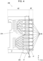
- the second layer 10b includes a flat plate-shaped base 11b including a dielectric, a ground conductor 13b, and through conductors 14b.
- the base 11b includes a first region R1 and a second region R2.
- the second layer 10b overlaps the first layer 10a such that the first region R1 of the base 11b and the first region R1 of the base 11a coincide in see-through plan view.
- the dashed lines indicate the areas overlapping the mounting region r1 and the frame region r2 in see-through plan view.
- the ground conductor 13b is formed on an upper surface of the base 11b.
- the ground conductor 13b includes portions overlapping the ground conductors 13a of the first layer 10a in see-through plan view and a portion connecting the ends of these portions in the -X direction together.
- the ground conductor 13b has the shape of a flat conductor from which portions are removed, the portions overlapping regions including and surrounding the signal conductors 12 of the first layer 10a in see-through plan view.
- An upper surface of the ground conductor 13b is connected to the through conductors 14a of the first layer 10a. Accordingly, the ground conductor 13b is electrically connected to the ground conductors 13a of the first layer 10a via the through conductors 14a and has the ground potential.
- the ground conductor 13b is also connected to the through conductors 14b extending through the base 11b in the Z direction.
- the second layer 10b is provided mainly to adjust the distance between the first layer 10a and the third layer 10c or to adjust the impedance of the terminal member 10. Therefore, the second layer 10b may be omitted when the adjustment of the distance or the impedance is not unnecessary.
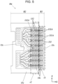
- the third layer 10c includes a flat plate-shaped base 11c including a dielectric, a ground conductor 13c (first ground conductor), and through conductors 14c.
- the base 11c includes a first region R1 and a second region R2.
- the third layer 10c overlaps the second layer 10b such that the first region R1 of the base 11c and the first region R1 of the base 11b coincide in see-through plan view.
- the base 11c has a shape that is substantially the same as the shape of the base 11b.
- the ground conductor 13c is formed on an upper surface of the base 11c.
- ⁇ is the wavelength of a high-frequency signal transmitted through the signal conductors 12
- the ground conductor 13c is located at a distance of less than ⁇ /4 from the signal conductors 12 in the direction perpendicular to the first surface S1 (Z direction).
- the ground conductor 13c includes portions overlapping the ground conductor 13b of the second layer 10b in see-through plan view.
- the ground conductor 13c also includes a plurality of first openings 131A in the first region R1.
- the ground conductor 13c also includes a plurality of second openings 132A in the second region R2 in an area within a predetermined distance in the -X direction from the boundary between the second region R2 and the first region R1.
- the second openings 132A are formed in an area overlapping the frame region r2 in see-through plan view. In a section further in the +Y direction than the center of the third layer 10c in the Y direction, the second openings 132A are also formed in an area that is further in the -X direction than the frame region r2, that is, in an area inside the cavity.
- the first openings 131A and the second openings 132A are arranged next to each other in the X direction and the Y direction in a matrix pattern.
- the ground conductor 13c includes the first openings 131A and the second openings 132A in a mesh pattern.
- the ground conductor 13c includes a first grid portion 131 and a second grid portion 132.
- the first grid portion 131 includes segments disposed between the first openings 131A that are adjacent to each other.
- the second grid portion 132 includes segments disposed between the second openings 132A that are adjacent to each other.
- Each of the first grid portion 131 and the second grid portion 132 is a conductor including straight segments extending in the X direction and the Y direction.
- the ground conductor 13c also includes a straight grid portion extending in the Y direction at the boundary between the first region R1 and the second region R2.
- the straight grid portion includes segments disposed between the first openings 131A and the second openings 132A that are adjacent to each other.
- the ground conductor 13c includes sixteen opening rows corresponding to the sixteen signal conductors 12. Each opening row overlaps one of the signal conductors 12 in see-through plan view. More specifically, the center of each opening row in the Y direction overlaps one of the signal conductors 12. Therefore, the segments of the first grid portion 131 extending in the Y direction and disposed between the first openings 131A adjacent to each other in the X direction in each opening row are orthogonal to the corresponding signal conductor 12 in see-through plan view.
- the ground conductor 13c includes the first grid portion 131 at a location (first location) overlapping the first region R1 and at least portions of the signal conductors 12 in see-through plan view.
- the ground conductor 13c also includes the second grid portion 132 at a location (second location) connected to the first grid portion 131 in the X direction and overlapping the second region R2 and at least portions of the signal conductors 12 in see-through plan view.
- ground conductor 13c An upper surface of the ground conductor 13c is connected to the through conductors 14b of the second layer 10b. Accordingly, the ground conductor 13c is electrically connected to the ground conductor 13b of the second layer 10b via the through conductors 14b and has the ground potential. The ground conductor 13c is also connected to the through conductors 14c extending through the base 11c in the Z direction.
- the first openings 131A and the second openings 132A have a rectangular shape with sides extending in the X direction (first direction) and the Y direction (second direction).
- the rectangular shape is not limited to a shape including four corners with precise right angles (rectangle).
- the second direction may also be referred to as a direction crossing the first direction.
- the rectangular shape includes a polygonal shape formed by chamfering one or more corners of a rectangle.
- a shape with a chamfered corner is a shape in which two of the four sides of a rectangle forming the corner are connected to each other with a side that is not parallel to either of the two sides.
- the rectangular shape may also include a shape in which the sides of a rectangle are connected with curves.
- the rectangular shape includes the shape of an opening designed to have the shape of a rectangle but formed as an opening with curved corners in practice due to limitations in manufacturing processes.
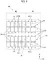
- the rectangular shape may also include a shape including one or more sides at which one or more protrusions P protrude, each protrusion P overlapping one of the through conductors 14c in plan view.
- the lengths of the first openings 131A and the second openings 132A in the X direction and the Y direction are ⁇ /8 or more and ⁇ /4 or less.
- the area of each of the first openings 131A is greater than the area of each of the second openings 132A. More specifically, the first openings 131A and the second openings 132A have the same width in the Y direction, and the width of each of the first openings 131A in the X direction is greater than the width of each of the second openings 132A in the X direction.
- the through conductors 14c are located on the first grid portion 131 and the second grid portion 132.
- the through conductors 14c are located to overlap the first grid portion 131 and the second grid portion 132 in plan view, and are connected to the first grid portion 131 and the second grid portion 132. More specifically, the through conductors 14c are located to overlap the segments of the first grid portion 131 extending in the X direction.
- the through conductors 14c are also located to overlap the grid portion extending in the Y direction at the boundary between the first region R1 and the second region R2.
- the through conductors 14c are also located at the intersections of the second grid portion 132.
- the through conductors 14c are also located around the first openings 131A and the second openings 132A.
- each through conductor 14c to an adjacent one of the through conductors 14c is less than ⁇ /4.
- at least one through conductor 14c is disposed within a distance of ⁇ /4 from each through conductor 14c on the XY plane.
- the through conductors 14b of the second layer 10b are located to overlap some of the through conductors 14c in see-through plan view.
- the through conductors 14b and 14c located in the second region R2 overlap in see-through plan view.
- the through conductors 14b and 14c are located at the intersections of the second grid portion 132 in see-through plan view. This enables a dense arrangement of the through conductors 14b and 14c in the region in which the second openings 132A are formed in a mesh pattern.
- each of the through conductors 14b and a corresponding one of the through conductors 14c are located on a straight line extending in the Z direction with one of the intersections of the second grid portion 132 disposed therebetween.
- the through conductors 14c are arranged at equal intervals in the X direction in the first region R1 and the second region R2.
- the arrangement is not limited to this.
- the intervals between the through conductors 14c in the first region R1 may be less than the intervals between the through conductors 14c in the second region R2.
- the through conductors 14c may be arranged more densely in first region R1 than in the second region R2.
- the through conductors 14c may be located at the intersections of the first grid portion 131.
- the fourth layer 10d includes a flat plate-shaped base 11d including a dielectric, a ground conductor 13d (second ground conductor), and through conductors 14d.
- the base 11d includes a first region R1 and a second region R2.
- the fourth layer 10d overlaps the third layer 10c such that the first region R1 of the base 11d and the first region R1 of the base 11c coincide in see-through plan view.
- the base 11d has a shape that is substantially the same as the shape of the base 11c in an area around the end thereof in the +X direction.
- the ground conductor 13d is formed on an upper surface of the base 11d.
- the ground conductor 13d is located at a distance of less than ⁇ /4 from the signal conductors 12 in the Z direction.
- the ground conductor 13d is further away from the first surface S1 than the ground conductor 13c of the third layer 10c. Therefore, the distance between the first surface S1 and the ground conductor 13d is greater than the distance between the first surface S1 and the ground conductor 13c.
- the ground conductor 13d includes a plurality of third openings 133A in a mesh pattern in the first region R1.
- the shape and area of each of the third openings 133A are respectively the same as the shape and area of each of the first openings 131A of the third layer 10c. Accordingly, the third openings 133A have a rectangular shape with sides extending in the X direction and the Y direction, and the lengths of the third openings 133A in the X direction and the Y direction are ⁇ /8 or more and ⁇ /4 or less.
- Each of the third openings 133A overlaps one of the first openings 131A in plan view.
- the ground conductor 13d includes a third grid portion 133 including segments disposed between the third openings 133A that are adjacent to each other.
- the third grid portion 133 is a conductor including straight segments extending in the X direction and the Y direction. Each opening row composed of the third openings 133A arranged in one row in the X direction overlaps one of the signal conductors 12 in see-through plan view, as each opening row composed of the first openings 131A.
- the segments of the third grid portion 133 extending in the Y direction are orthogonal to the signal conductors 12 in see-through plan view.
- the ground conductor 13d includes the third grid portion 133 at a location (third location) overlapping the first region R1 and at least portions of the signal conductors 12 in see-through plan view.
- the ground conductor 13d may include additional openings located to overlap the second openings 132A of the third layer 10c.
- the area of the third openings 133A may be less than the area of the first openings 131A within a range such that the lengths of the third openings 133A in the X direction and the Y direction are ⁇ /8 or more and ⁇ /4 or less.
- ground conductor 13d An upper surface of the ground conductor 13d is connected to the through conductors 14c of the third layer 10c. Accordingly, the ground conductor 13d is electrically connected to the ground conductor 13c of the third layer 10c via the through conductors 14c and has the ground potential. The ground conductor 13d is also connected to the through conductors 14d extending through the base 11d in the Z direction.
- the fifth layer 10e includes a flat plate-shaped base 11e including a dielectric, a ground conductor 13e, and through conductors 14e.
- the base 11e includes a first region R1 and a second region R2.
- the fifth layer 10e overlaps the fourth layer 10d such that the first region R1 of the base 11e and the first region R1 of the base 11d coincide in see-through plan view.
- the base 11e has a shape that is substantially the same as the shape of the base 11d.
- ground conductor 13e An upper surface of the ground conductor 13e is connected to the through conductors 14d of the fourth layer 10d. Accordingly, the ground conductor 13e is electrically connected to the ground conductor 13d of the fourth layer 10d via the through conductors 14d and has the ground potential.
- the ground conductor 13e is a solid conductor formed in a region including locations overlapping the third openings 133A of the fourth layer 10d in plan view. The ground conductor 13e extends over the mounting region r1 and a portion of the frame region r2.
- the ground conductor 13e is also connected to the through conductors 14e extending through the base 11e in the Z direction.
- the through conductors 14e are connected to a ground conductor included in a sixth layer below the through conductors 14e.
- the ground conductor of the sixth layer may be connected to a ground conductor of a seventh layer below the sixth layer by through conductors extending through a base of the sixth layer.
- the ground potential can be stabilized by electrically connecting the ground conductors of multiple layers with the through conductors.
- the through conductors 14e may be omitted when the terminal member 10 include no layers below the sixth layer.
- the base 11 of the terminal member 10 includes the bases 11a to 11e included in the first to fifth layers 10a to 10e, respectively.
- the ground conductor 13 of the terminal member 10 includes the ground conductors 13a to 13e included in the first to fifth layers 10a to 10e, respectively.
- the ground conductors 13b to 13e are located in the base 11.
- the terminal member 10 may be formed by, for example, the following method.
- the material of the bases 11a to 11e may be, for example, a ceramic sintered body, such as an aluminum-oxide-based sintered body, an aluminum-nitride-based sintered body, a silicon-carbide-based sintered body, a mullite-based sintered body, or a glass ceramic.
- a ceramic sintered body such as an aluminum-oxide-based sintered body, an aluminum-nitride-based sintered body, a silicon-carbide-based sintered body, a mullite-based sintered body, or a glass ceramic.
- the base 11 of the terminal member 10 may be manufactured as follows. First, material powder is mixed with an organic solvent and a binder to form a slurry.
- the main components of the material powder are aluminum oxide powder and powder of silicon oxide or the like serving as a sintering aid component.
- the slurry is formed into sheets by a forming method, such as the doctor blade method or the lip coater method.
- a forming method such as the doctor blade method or the lip coater method.
- ceramic green sheets hereinafter also referred to as green sheets
- the green sheets are stacked together to form a multilayer body.
- the multilayer body is fired at a temperature of about 1300°C to about 1600°C to obtain the base 11.
- the signal conductors 12 and the ground conductors 13a to 13e composed of metallized layers of tungsten, for example, may be formed by mixing tungsten powder with an organic solvent and an organic binder to form a metal paste, printing the metal paste on the green sheets at predetermined positions by screen printing, and firing the metal paste.
- the through conductors 14a to 14e may be formed by forming through holes in the green sheets at predetermined positions prior to the printing of the metal paste, filling the through holes with a metal paste that is the same as or similar to the above-described metal paste, and firing the metal paste together with the green sheets.
- a nickel film with a thickness of about 1 to 10 ⁇ m and a gold film with a thickness of about 0.1 to 3 ⁇ m may be successively formed on surfaces of conductor layers, such as the signal conductors 12 and the ground conductors 13a, that are exposed to the outside to protect the surfaces and facilitate bonding with a brazing material, solder, or the like.
- the wiring base 100 includes the terminal member 10 of the above-described structure. Therefore, the impedance of the terminal member 10 can be adjusted to an appropriate value. This will now be described.
- the wiring base 100 is configured such that the ground conductor 13c below the signal conductors 12 includes the first openings 131A in a mesh pattern in the mounting region r1 (first region R1). Accordingly, the resonant frequency can be maintained, and reduction in the impedance can be reduced to enable adjustment of the impedance to a desired value.
- the above-described wiring base 100 has good transmission characteristics for high-frequency signals.
- the second openings 132A in a mesh pattern are formed in a region further toward the cavity than the mounting region r1, that is, in the frame region r2 and in the cavity. Accordingly, the resonance frequency in a region around the mounting region r1 can be shifted toward higher frequencies. Therefore, the wiring base 100 of the above-described structure has good transmission characteristics for high-frequency signals. In addition, reduction in the impedance can be reduced.
- the resonant frequency of the microstrip line greatly depends on the cross-sectional shape of the wiring lines on a plane perpendicular to a signal transmission direction. Therefore, the resonant frequency is generally adjusted by adjusting the shapes of the signal conductors and the ground conductor in the mounting region r1.
- the electromagnetic field generated in the mounting region r1 also extends in a direction toward the cavity, and the shapes of the conductors extending in a direction parallel to the signal transmission direction, that is, the shapes of the conductors extending from the mounting region r1 and into the cavity, also affect the resonant frequency. Therefore, the wiring base 100, in which the ground conductor 13 includes the second openings 132A in a mesh pattern in a region further toward the cavity than the mounting region r1, has good transmission characteristics for high-frequency signals.
- the fourth layer 10d also includes the third openings 133A in a mesh pattern in the mounting region r1.
- the openings in a mesh pattern are formed in two layers. Accordingly, reduction in the impedance can be further reduced.
- the signal conductors 12 include the signal terminals 12T in the mounting region r1.
- the signal terminals 12T has a line width (width in the Y direction in FIG. 3 ) with a lower limit determined by the design requirements for appropriate mounting of the external board 2. Therefore, the impedance may be reduced to a value below the desired value.
- reduction in the impedance can be reduced to enable adjustment of the impedance to the desired value.
- Reduction in the impedance can also be reduced by setting the area of the first openings 131A to an area greater than the area of the second openings 132A.
- the line width of each of the signal conductors 12 is not limited in a region further toward the cavity than the mounting region r1, for example, in the frame region r2. Therefore, reduction in the impedance can be reduced by reducing the width of each of the signal conductors 12. Accordingly, the area of the second openings 132A may be less than the area of the first openings 131A of the third layer 10c.
- the fourth layer 10d includes no openings in the second region R2 including the frame region r2. However, the fourth layer 10d is not limited to this, and may include openings in the second region R2 to enable further adjustment of the impedance.
- the wiring base 100 of the above-described structure has good transmission characteristics for high-frequency signals.
- the impedance can be adjusted in consideration of the effective relative dielectric constant in regions in which the openings are formed. This will now be described.
- the resonant frequency shifts toward higher frequencies as the size of the openings in a mesh pattern decreases.
- the impedance decreases as the size of the openings in a mesh pattern decreases. Therefore, the size of the openings is desirably increased while a high resonant frequency is maintained by setting the lengths of the openings to ⁇ /4 or less.
- the effective relative dielectric constant is lower than that in the frame region r2, which is in contact with the ceramic frame 22. Therefore, the wavelength ⁇ of electromagnetic waves is longer in the mounting region r1 than in the frame region r2 when the frequency is constant.
- the first openings 131A formed in the mounting region r1 can be further increased in size while the condition that "the lengths of the openings are ⁇ /4 or less" is satisfied.
- reduction in the impedance can be reduced without causing a shift of the resonant frequency toward lower frequencies.
- the wiring base 100 of the above-described structure has good transmission characteristics for high-frequency signals.
- the openings in a mesh pattern can be provided within an area in which the electromagnetic waves propagate. Accordingly, reduction in the impedance can be reduced. Therefore, the wiring base 100 of the above-described structure has good transmission characteristics for high-frequency signals.
- the ground conductor 13e is disposed on the layer below the ground conductor 13d including the third openings 133A.
- the ground conductor 13e is a solid conductor formed over a region including locations overlapping the third openings 133A in plan view. Accordingly, radiation of the electromagnetic waves that pass through the first openings 131A and the third openings 133A to the outside of the electronic device 1 can be reduced.
- ground conductors 13c and 13d including the openings in a mesh pattern are electrically connected to each other via the through conductors 14c, the ground potential can be stabilized (enhanced). Accordingly, the transmission characteristics for high-frequency signals can be improved.
- the ground conductors 13c and 13d are also electrically connected to the ground conductors 13a, 13b, and 13e (and the ground conductors of the sixth and seventh layers that are further below) by other through conductors. Therefore, the ground potential can be further stabilized.
- leakage of electromagnetic waves generated by the transmission of a high-frequency signal in a direction toward the cavity can be reduced.
- leakage of the electromagnetic waves can be reduced by arranging the through conductors 14c more densely in the first region R1 (mounting region r1), in which the resonant frequency easily varies upon connection with the external board, than in the second region R2.
- the through conductors 14c are located at the intersections of the first grid portion 131, and when the through conductors 14c are located at the intersections of the second grid portion 132, the through conductors 14c can be more densely arranged.
- the through conductors 14c are preferably arranged at a high density.
- the electrical connection between the ground conductors via the through conductors can be enhanced, and the ground potential can be stabilized accordingly.
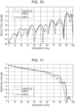
- the solid lines indicate the simulation results of an example in which the first openings 131A, the second openings 132A, and the third openings 133A in a mesh pattern according to the present embodiment are provided.
- the dashed lines indicate the simulation results of a comparative example in which the ground conductor 13 of the terminal member 10 includes no openings in a mesh pattern.
- the reflection loss (reflection of input increases as the reflection loss approaches 0) of the example is less than the reflection loss of the comparative example.
- the insertion loss (loss increases as the absolute value of the insertion loss increases) of the example is less than the insertion loss of the comparative example.
- the wiring base 100 includes the base 11, the signal conductors 12, and the ground conductor 13 including the ground conductor 13c as the first ground conductor.
- the base 11 includes the first surface S1, the first region R1, and the second region R2.
- the first region R1 is located near the outer side of the first surface S1.
- the external board 2 is mounted in the first region R1.
- the second region R2 is other than the first region R1.
- the signal conductors 12 extend along a region including the first region R1 of the first surface S1 in the X direction away from the outer side.
- the ground conductor 13c is located in the base 11 at a distance from the signal conductors 12 of less than 1/4 of the wavelength ⁇ of the high-frequency signal in the direction perpendicular to the first surface S1, the high-frequency signal being transmitted through the signal conductors 12.
- the ground conductor 13c includes the first grid portion 131 at the first location overlapping the first region R1 and at least portions of the signal conductors 12 in see-through plan view viewed in a direction toward the first surface S1.
- the first grid portion 131 includes the segments disposed between the first openings 131A.
- the lengths of the first openings 131A in the X direction and the Y direction are ⁇ /8 or more and ⁇ /4 or less.
- the through conductors 14c are located on the first grid portion 131.
- the impedance can be adjusted to a desired value while the resonant frequency is maintained.
- the through conductors 14c provide electrical connection between the ground conductor 13c and another ground conductor, the ground potential can be stabilized (enhanced).
- transmission characteristics for high-frequency signals can be improved.
- the first openings 131A have a rectangular shape with sides extending in the X direction and the Y direction, the first openings 131A having a desired area can be easily designed.
- the through conductors 14c When the through conductors 14c are located at the intersections of the first grid portion 131, the through conductors 14c can be more densely arranged.
- the ground conductor 13c includes the second grid portion 132 at the second location connected to the first grid portion 131 in the X direction and overlapping the second region R2 in see-through plan view.
- the second grid portion 132 includes the segments disposed between the second openings 132A.
- the lengths of the second openings 132A in the X direction and the Y direction are ⁇ /8 or more and ⁇ /4 or less.
- the area of the second openings 132A is less than the area of the first openings 131A. Accordingly, the frequency of the resonance that occurs around the mounting region r1 can be shifted toward higher frequencies to improve the transmission characteristics for high-frequency signals. In addition, reduction in the impedance can be further reduced. Since the area of the second openings 132A is less than the area of the first openings 131A, the impedance can be adjusted in consideration of the effective relative dielectric constant in regions in which the openings are formed.
- the second openings 132A have a rectangular shape with sides extending in the X direction and the Y direction, the second openings 132A having a desired area can be easily designed.
- the through conductors 14c When the through conductors 14c are located at the intersections of the second grid portion 132, the through conductors 14c can be more densely arranged.
- the ground conductor 13 is located in the base 11 at a distance of less than ⁇ /4 from the signal conductors 12 in the direction perpendicular to the first surface S1.
- the ground conductor 13 includes the ground conductor 13d as the second ground conductor.
- the ground conductor 13d includes the third grid portion 133 at a third location overlapping the first region R1 and at least portions of the signal conductors 12 in see-through plan view.
- the third grid portion 133 includes segments disposed between the third openings 133A. The lengths of the third openings 133A in the X direction and the Y direction are ⁇ /8 or more and ⁇ /4 or less.
- the ground conductor 13d is further away from the first surface S1 than the ground conductor 13c in the direction perpendicular to the first surface S1, and is connected to the ground conductor 13c via the through conductors 14c.
- the openings in a mesh pattern are formed in two layers, and therefore reduction in the impedance can be further reduced.
- the electrical connection between the ground conductors can be enhanced, and the ground potential can be stabilized accordingly.
- the third openings 133A have a rectangular shape with sides extending in the X direction and the Y direction, the third openings 133A having a desired area can be easily designed.
- the third openings 133A overlap the first openings 131A in see-through plan view.
- the openings in a mesh pattern are formed in two layers, and therefore reduction in the impedance can be reduced.
- the impedance can be adjusted within a desired range, and the design flexibility for the adjustment of the resonant frequency, for example, can be increased. Such an adjustment is enabled because the fourth layer 10d including the third openings 133A is further away from the signal conductors 12 than the third layer 10c including the first openings 131A.
- the wiring base 100 includes the through conductors 14c, and the distance between adjacent ones of the through conductors 14c is less than ⁇ /4. Accordingly, leakage of electromagnetic waves generated by the transmission of a high-frequency signal in a direction toward the cavity can be reduced. The electrical connection between the ground conductors via the through conductors can be enhanced, and accordingly the ground potential can be stabilized.
- the electronic device 1 includes the above-described wiring base 100 and the electronic component 200 connected to the wiring base 100. Therefore, the electronic device 1 has good transmission characteristics for high-frequency signals.
- the structure of the terminal member 10 differs from that in the first embodiment.
- the difference from the first embodiment will be described.
- the electronic device 1 and the wiring base 100 can be used for optical communication in a higher frequency band (for example, the modulation rate is about 128 Gbaud or less and the frequency band is about 95 GHz or less).
- the structure of the terminal member 10 according to the second embodiment will be described with reference to FIG. 12 .
- the terminal member 10 includes a four-layer structure composed of a first layer 10a, a second layer 10b, a third layer 10c, and a fourth layer 10d.
- the first layer 10a includes a base 11a, eight signal conductors 12, five ground conductors 13a, and through conductors 14a. Also in the second embodiment, the base 11a includes a first region R1 in which the external board 2 is mounted and a second region R2 including a frame region r2.
- the second layer 10b includes a base 11b, a ground conductor 13b, and through conductors 14b.
- the ground conductor 13b corresponds to the "first ground conductor".
- the ground conductor 13b includes first openings 131A in the first region R1.
- the ground conductor 13b includes a first grid portion 131 including segments disposed between the first openings 131A.
- the ground conductor 13b includes no second openings 132A.
- the second openings 132A may be formed when the second openings 132A are necessary for impedance adjustment.
- the third layer 10c includes a base 11c and a ground conductor 13c.
- the ground conductor 13c corresponds to the "second ground conductor”.
- the ground conductor 13c includes third openings 133A.
- the third openings 133A overlap the first openings 131A in see-through plan view.
- the ground conductor 13c includes a third grid portion 133 including segments disposed between the third openings 133A.
- the third layer 10c includes no through conductors.
- the fourth layer 10d is composed of a dielectric base 11d, and include no conductors, such as a ground conductor and through conductors.
- neither the first openings 131A nor the third openings 133A overlap the ground conductor 13 in see-through plan view.
- no solid conductor is located to overlap the first openings 131A or the third openings 133A in see-through plan view. Accordingly, reduction in the impedance can be further reduced.
- the resonant frequency can be further shifted toward higher frequencies to improve the transmission characteristics for high-frequency signals. Although an increase in the resonant frequency tends to cause a cavity resonance in which standing waves are generated in the cavity, the cavity resonance can be reduced because no solid conductor is provided (no shielding is provided) at the bottom layer. Accordingly, degradation of the transmission characteristics for high-frequency signals due to the influence of the cavity resonance can be reduced, and the resonant frequency can be further shifted toward higher frequencies.
- a terminal member 10 according to an embodiment other than the first and second embodiments will be described with reference to FIG. 13 .
- FIG. 13 is an enlarged partial view of the terminal member 10.
- FIG. 13 illustrates a first layer 10a and a second layer 10b of the terminal member 10.
- the second layer 10b is placed on a lower surface of the first layer 10a.
- a plurality of signal conductors 12 is formed on an upper surface of a base 11a of the first layer 10a.
- a ground conductor 13b is formed on an upper surface of a base 11b of the second layer 10b.
- the base 11a includes a groove 15 extending through the base 11a in the Z direction at a location between two adjacent ones of the signal conductors 12.
- the base 11 of the terminal member 10 includes the groove 15 extending from a first surface S1 to the layer including the ground conductor 13b serving as the first ground conductor.
- the groove 15 has an elongated circular shape extending in the direction in which the signal conductors 12 extend (X direction) in FIG. 13
- the shape of the groove 15 is not limited to this, and may be, for example, a rectangular shape.
- the groove 15 may be a cut extending to an end of the base 11a.
- the ground conductor 13b partially overlaps the signal conductors 12 in see-through plan view.
- the ground conductor 13b includes a plurality of first openings 131A in a mesh pattern.
- the first openings 131A partially overlap the signal conductors 12 in see-through plan view.
- the first openings 131A also partially overlap the groove 15 in see-through plan view.
- the first openings 131A are partially exposed at the groove 15 when viewed in the Z direction (that is, in see-through plan view viewed in the direction toward the first surface S1).
- the ground conductor 13b of the second layer 10b is also partially exposed at the groove 15 when viewed in the Z direction.
- the relative dielectric constant can be reduced in the region in which the groove 15 is formed. Therefore, reduction in the impedance of the signal conductors 12 can be reduced. Reduction in the impedance of the signal conductors 12 can also be reduced by forming the first openings 131A in a mesh pattern in the ground conductor 13b.
- reduction in the impedance caused when the signal conductors 12 are brought closer to the ground conductor 13b to broaden the frequency band of the transmission line can be reduced, and the impedance can be adjusted to a desired value. Accordingly, the transmission characteristics for high-frequency signals can be improved, and the frequency band can be broadened.
- the groove 15 may be T-shaped. More specifically, the groove 15 is preferably shaped to include portions disposed on the extensions of the signal conductors 12 in the signal transmission direction. More specifically, the groove 15 preferably includes a portion extending in the X direction (signal transmission direction) at a location between the two adjacent signal conductors 12; a portion extending in the +Y direction from an end portion, in the +X direction, of the portion extending in the X direction; and a portion extending in the -Y direction from the end portion.
- the X direction signal transmission direction
- the portion of the groove 15 extending in the +Y direction and the portion of the groove 15 extending in the -Y direction preferably extend to locations overlapping the extensions of the signal conductors 12 when the signal conductors 12 are extended in the +X direction.
- an external board such as an FPC
- reduction in the impedance of the signal conductors 12 due to the connection to the external board can be reduced in regions around the connecting portions. Accordingly, high-frequency characteristics of the signal conductors 12, in particular, high-frequency characteristics in a common mode, can be improved.
- first openings 131A, the second openings 132A, and the third openings 133A have a rectangular shape with sides extending in the X direction and the Y direction in the above-described embodiments, the shape is not limited to this.
- first openings 131A, the second openings 132A, and the third openings 133A may have a shape with sides extending in a first direction and a second direction that are not orthogonal to each other, for example, the shape of a parallelogram or a rhomboid.
- first openings 131A, the second openings 132A, and the third openings 133A may have a polygonal shape other than a rectangular shape, a circular shape, or an elliptical shape.
- the openings of one or two groups may have a rectangular shape while the openings of the remaining group or groups have any of the above-described non-rectangular shapes.
- the openings in a mesh pattern are formed in two layers in the above-described embodiments, the openings are not limited to this.
- the number of layers in which the openings in a mesh pattern are formed may be one or three or more.
- the present disclosure is applicable to wiring bases and electronic devices.
Landscapes
- Engineering & Computer Science (AREA)
- Microelectronics & Electronic Packaging (AREA)
- Physics & Mathematics (AREA)
- Electromagnetism (AREA)
- Structure Of Printed Boards (AREA)
- Production Of Multi-Layered Print Wiring Board (AREA)
Abstract
Description
- The present disclosure relates to a wiring base and an electronic device.
- A known wiring base (for example, a package) includes an electronic component mounted therein and provides electrical connection between the electronic component and an external wiring line. The wiring base may include a main body containing the electronic component and a terminal member extending out of the main body. The terminal member includes a signal conductor and a ground conductor that are electrically connected to the electronic component. When an external board is mounted to the terminal member, a wiring line of the external board is electrically connected to the electronic component.
- A known terminal member includes a signal line (microstrip line) that enables transmission of a high-frequency signal. The signal line includes a signal conductor and a ground conductor facing the signal conductor across an insulator. International Publication No.
2010/103722 , for example, describes a technology for adjusting the impedance of the signal line by forming openings in a mesh pattern in the ground conductor of the terminal member. - According to an aspect of the present disclosure, a wiring base includes a base, a signal conductor, and a ground conductor including a first ground conductor. The base includes a first surface, a first region, and a second region. The first region is located near an outer side of the first surface. An external board is mounted in the first region. The second region is other than the first region. The signal conductor extends through a region including the first region of the first surface in a first direction away from the outer side. The first ground conductor is located in the base at a distance from the signal conductor of less than 1/4 of a wavelength of a high-frequency signal in a direction perpendicular to the first surface. The high-frequency signal is transmitted through the signal conductor. The first ground conductor includes a first grid portion at a first location overlapping the first region and at least a portion of the signal conductor in a see-through plan view viewed in a direction toward the first surface. The first grid portion includes a segment disposed between first openings. Lengths of the first openings in the first direction and a second direction crossing the first direction are 1/8 or more and 1/4 or less of the wavelength of the high-frequency signal. A through conductor is located on the first grid portion.
- According to another aspect of the present disclosure, an electronic device includes the above-described wiring base and an electronic component connected to the wiring base.
-
-
FIG. 1 is a perspective view of an electronic device according to a first embodiment. -
FIG. 2 is a plan view of the electronic device and a wiring base. -
FIG. 3 illustrates a first layer of a terminal member. -
FIG. 4 illustrates a second layer of the terminal member. -
FIG. 5 illustrates a third layer of the terminal member. -
FIG. 6 is an enlarged view of the third layer of the terminal member. -
FIG. 7 is an enlarged view illustrating another example of the third layer of the terminal member. -
FIG. 8 illustrates a fourth layer of the terminal member. -
FIG. 9 illustrates a fifth layer of the terminal member. -
FIG. 10 illustrates the result of a simulation of reflection loss of the wiring base. -
FIG. 11 illustrates the result of a simulation of insertion loss of the wiring base. -
FIG. 12 illustrates first to fourth layers of a terminal member according to a second embodiment. -
FIG. 13 illustrates a terminal member according to another embodiment. -
FIG. 14 illustrates a terminal member according to another embodiment. - Embodiments will be described with reference to the drawings. Note that, for convenience of description, the drawings referred to below are simplified and illustrate only main components necessary to describe the embodiments. Therefore, a
wiring base 100 and anelectronic device 1 according to the present disclosure may include any components that are not illustrated in the drawings referred to below. Dimensions of components illustrated in the drawings do not accurately reflect the actual dimensions and dimensional ratios of the components. - The structure of the
electronic device 1 according to a first embodiment will be described with reference toFIGs. 1 and2 . - The
electronic device 1 includes thewiring base 100 and anelectronic component 200. Theelectronic device 1 also includes alid body 30 sealing thewiring base 100. - The
wiring base 100 includes amain body 20 and aterminal member 10. Theterminal member 10 extends out of themain body 20. When theelectronic device 1 includes thelid body 30, thelid body 30 may be regarded as sealing themain body 20. Thewiring base 100 is an electronic device package including themain body 20 in which theelectronic component 200 is mounted. The electronic device package provides electrical connection between theelectronic component 200 and wiring lines of anexternal board 2 through theterminal member 10. In the present embodiment, thewiring base 100 holds, for example, theelectronic component 200 for optical communication. In this case, theelectronic component 200 may receive or output a high-frequency signal for optical communication (for example, the modulation rate is about 96 Gbaud or less and the frequency band is about 75 GHz or less). For example, theelectronic component 200 may be a light emitting element or a light receiving element. These are examples, and theelectronic component 200 to be mounted is not limited to the above-described elements. - The
main body 20 includes abottom portion 21, aframe 22, and aseal member 23. Thebottom portion 21 is a rectangular plate-shaped member. In the following description, directions parallel to the sides of therectangular bottom portion 21 are referred to as an X direction and a Y direction, and a direction perpendicular to thebottom portion 21 and extending from thebottom portion 21 toward thelid body 30 is referred to as a Z direction. Among surfaces of any component that are parallel to the XY plane, a surface facing in the +Z direction is referred to as an "upper surface", and a surface facing in the -Z direction is referred to as a "lower surface". A layer located in the -Z direction relative to another object is referred to as a layer "below" the object. A view in the Z direction is referred to as a "plan view", and a see-through view seen through other components in the Z direction is referred to as a "see-through plan view". - An upper surface of the
bottom portion 21 includes a placement region in which theelectronic component 200 is placed. Theelectronic component 200 placed in the placement region includes terminals electrically connected to wiring lines formed on the upper surface of thebottom portion 21. - The
frame 22 is a frame-shaped member surrounding the placement region for theelectronic component 200 in plan view. In the present embodiment, theframe 22 extends in the +Z direction from an outer peripheral portion of thebottom portion 21 to form a frame-shaped side wall. Theframe 22 may include throughholes 22a for allowing optical fibers or the like to extend therethrough. - Each of the
bottom portion 21 and theframe 22 may, for example, include a plurality of insulative boards stacked in the Z direction. Each insulative board may be, for example, a ceramic sintered body, such as an aluminum-oxide-based sintered body, an aluminum-nitride-based sintered body, a silicon-carbide-based sintered body, a mullite-based sintered body, or a glass ceramic. Theframe 22 may be separate from thebottom portion 21 or be formed integrally with thebottom portion 21. - The
seal member 23 is disposed on an upper surface of theframe 22. Theseal member 23 may be used as a material for sealing themain body 20 with thelid body 30 in an airtight manner after theelectronic component 200 is mounted on thebottom portion 21. Theseal member 23 may be formed by, for example, joining a frame-shaped metal plate to a frame-shaped conductor by brazing with a brazing material or the like. The frame-shaped conductor is formed from a conductor paste containing a high-melting-point metal, such as tungsten or molybdenum. The frame-shaped metal plate includes a metal plate made of a Fe-Ni-based alloy or a Fe-Ni-Co-based alloy. - The
lid body 30 is a plate-shaped member having substantially the same shape as the shape of thebottom portion 21 in plan view. Thelid body 30 may be any member capable of reducing entrance of foreign matter, such as moisture and fine particles, into theelectronic device 1. Thelid body 30 may be obtained by, for example, forming the same metal material as the material of theseal member 23, the same ceramic material as the material of thebottom portion 21 and theframe 22, or the like into a plate shape. In the following description, a space defined by thebottom portion 21, theframe 22, and thelid body 30 is referred to as a cavity. - A side wall of the
frame 22 at an end of theframe 22 in the +X direction includes afitting portion 22b extending through the side wall in a thickness direction (X direction). Theterminal member 10 is shaped to fit thefitting portion 22b. Theterminal member 10 extends from a location inside (in the -X direction from) thefitting portion 22b to a location outside (in the +X direction from) thefitting portion 22b, and blocks thefitting portion 22b. Theterminal member 10 is fitted to thefitting portion 22b and fixed to theframe 22 with a brazing material or the like. Theterminal member 10 may be a portion of a multilayer structure of theframe 22. - The
terminal member 10 includes a base 11 including a dielectric, signalconductors 12, and aground conductor 13. Theterminal member 10 includes a portion protruding from themain body 20 and having a first surface S1 facing in the +Z direction. Thesignal conductors 12 and theground conductor 13 are partially exposed at the first surface S1. As illustrated inFIG. 1 , theexternal board 2 is connected to the first surface S1. Accordingly, the wiring lines on a surface of theexternal board 2 facing in the -Z direction are electrically connected to thesignal conductors 12 and theground conductor 13 on the first surface S1 of theterminal member 10. Thesignal conductors 12 and theground conductor 13 are electrically connected to terminals of theelectronic component 200 by the wiring lines formed on thebottom portion 21 or the like. Thus, theterminal member 10 provides electrical connection between the wiring lines on theexternal board 2 and the terminals of theelectronic component 200. - The structure of the
terminal member 10 will now be described in detail with reference toFIGs. 3 to 9 . - The
terminal member 10 includes afirst layer 10a (FIG. 3 ), asecond layer 10b (FIG. 4 ), athird layer 10c (FIGs. 5 and6 ), afourth layer 10d (FIG. 8 ), and afifth layer 10e (FIG. 9 ). Thefirst layer 10a to thefifth layer 10e are stacked in that order in the -Z direction. Thefirst layer 10a is located furthest in the +Z direction. Theterminal member 10 may further include a sixth layer and a seventh layer located further in the -Z direction than thefifth layer 10e. - As illustrated in
FIG. 3 , thefirst layer 10a includes abase 11a, thesignal conductors 12,ground conductors 13a, and throughconductors 14a. Thebase 11a is a flat plate-shaped dielectric and includes the first surface S1 (upper surface). Thebase 11a also includes a first region R1 and a second region R2. The first region R1 is near an outer side of the first surface S1 (side extending in the Y direction at an end in the +X direction), and theexternal board 2 is mounted in the first region R1. The second region R2 is other than the first region R1. - The first region R1 of the
base 11a is a rectangular region extending in the Y direction in plan view, and is exposed to the outside of thewiring base 100. Theexternal board 2 is connected and mounted to the first region R1. InFIG. 3 , the dashed line rectangle indicates a mounting region r1 in which theexternal board 2 is connected in plan view. - The second region R2 of the
base 11a includes a frame region r2 disposed adjacent to the first region R1 and overlapping theframe 22 in plan view. The second region R2 extends beyond the frame region r2 into the inside of the frame 22 (that is, the inside of the cavity). - The
signal conductors 12 and theground conductors 13a are formed on an upper surface of thebase 11a. - The
signal conductors 12 extend along a region including the first region R1 of the first surface S1 in a first direction (X direction) away from the outer side. Thesignal conductors 12 may extend straight in the X direction in the first region R1 and the frame region r2 of the second region R2. Thesignal conductors 12 may extend in a curved manner to predetermined locations at an end portion in the -X direction in a portion of the second region R2 corresponding to the inside of the cavity. Thesignal conductors 12 may include portions disposed in the first region R1 and serving asrectangular signal terminals 12T. Thesignal terminals 12T have a predetermined width in the Y direction to enable electrical connection to the wiring lines on theexternal board 2. Thesignal conductors 12 may include portions disposed in the frame region r2 and having a width less than that of thesignal terminals 12T in the Y direction. In the present embodiment, theterminal member 10 includes sixteensignal conductors 12. The number ofsignal conductors 12 may be changed as appropriate in accordance with the number of terminals of theelectronic component 200 that is mounted. - The
ground conductors 13a extend along a region including the first region R1 of the first surface S1 in the first direction (X direction) away from the outer side. Theground conductors 13a may extend straight in the X direction in the first region R1 and the frame region r2 of the second region R2. Theground conductors 13a may extend in a curved manner to predetermined locations at the end portion in the -X direction in the portion of the second region R2 corresponding to the inside of the cavity. Thesignal conductors 12 include portions disposed in the first region R1 and serving asground terminals 13T to which the wiring lines on theexternal board 2 are connected. - In the present embodiment, the
terminal member 10 includes nineground conductors 13a. Eachground conductor 13a has a ground potential. Two of theground conductors 13a are located on both sides of the sixteensignal conductors 12, that is, at both ends of thefirst layer 10a in the Y direction. The remaining sevenground conductors 13a are located such that two of thesignal conductors 12 are disposed between adjacent ones of theground conductors 13a. In other words, theground conductors 13a and thesignal conductors 12 are arranged in the Y direction in a periodic pattern of oneground conductor 13a, twosignal conductors 12, oneground conductor 13a, and so on. The number ofground conductors 13 may be changed as appropriate in accordance with the number of terminals of theelectronic component 200 that is mounted. - The
base 11a may include agroove 15 between each pair of adjacent ones of thesignal terminals 12T with noground terminal 13T disposed therebetween. Thegroove 15 is filled with air and have a low relative dielectric constant. Therefore, the electric field coupling between the pair ofsignal terminals 12T is reduced compared to when nogroove 15 is provided. Thegroove 15 may extend to an end of thebase 11a or be formed only between thesignal terminals 12T. Accordingly, adverse effects, such as cross-talk noise, caused by electromagnetic interference between thesignal terminals 12T can be reduced. Thewiring base 100 of the above-described structure has good transmission characteristics for high-frequency signals. - Each
ground conductor 13a may be connected to the throughconductors 14a extending through thebase 11a in the Z direction. InFIG. 3 , the circular dots indicate the locations of the through conductors 14. The through conductors 14 are arranged at regular intervals along the contours of theground conductors 13a in regions overlapping theground conductors 13a in see-through plan view. In the frame region r2, the through conductors 14 are formed between each pair of adjacent ones of thesignal conductors 12 with noground conductor 13a disposed therebetween. The throughconductors 14a may, for example, have a cylindrical shape. However, the shape of the throughconductors 14a is not limited to this. This also applies to throughconductors 14b to 14e described below. - As illustrated in
FIG. 4 , thesecond layer 10b includes a flat plate-shapedbase 11b including a dielectric, aground conductor 13b, and throughconductors 14b. Thebase 11b includes a first region R1 and a second region R2. Thesecond layer 10b overlaps thefirst layer 10a such that the first region R1 of thebase 11b and the first region R1 of thebase 11a coincide in see-through plan view. InFIG. 4 (and also inFIGs. 5 ,8 , and9 ), the dashed lines indicate the areas overlapping the mounting region r1 and the frame region r2 in see-through plan view. - The
ground conductor 13b is formed on an upper surface of thebase 11b. Theground conductor 13b includes portions overlapping theground conductors 13a of thefirst layer 10a in see-through plan view and a portion connecting the ends of these portions in the -X direction together. In another respect, theground conductor 13b has the shape of a flat conductor from which portions are removed, the portions overlapping regions including and surrounding thesignal conductors 12 of thefirst layer 10a in see-through plan view. An upper surface of theground conductor 13b is connected to the throughconductors 14a of thefirst layer 10a. Accordingly, theground conductor 13b is electrically connected to theground conductors 13a of thefirst layer 10a via the throughconductors 14a and has the ground potential. Theground conductor 13b is also connected to the throughconductors 14b extending through the base 11b in the Z direction. - The
second layer 10b is provided mainly to adjust the distance between thefirst layer 10a and thethird layer 10c or to adjust the impedance of theterminal member 10. Therefore, thesecond layer 10b may be omitted when the adjustment of the distance or the impedance is not unnecessary. - As illustrated in
FIG. 5 , thethird layer 10c includes a flat plate-shapedbase 11c including a dielectric, aground conductor 13c (first ground conductor), and throughconductors 14c. Thebase 11c includes a first region R1 and a second region R2. Thethird layer 10c overlaps thesecond layer 10b such that the first region R1 of thebase 11c and the first region R1 of thebase 11b coincide in see-through plan view. Thebase 11c has a shape that is substantially the same as the shape of thebase 11b. - The
ground conductor 13c is formed on an upper surface of thebase 11c. When λ is the wavelength of a high-frequency signal transmitted through thesignal conductors 12, theground conductor 13c is located at a distance of less than λ/4 from thesignal conductors 12 in the direction perpendicular to the first surface S1 (Z direction). Theground conductor 13c includes portions overlapping theground conductor 13b of thesecond layer 10b in see-through plan view. Theground conductor 13c also includes a plurality offirst openings 131A in the first region R1. Theground conductor 13c also includes a plurality ofsecond openings 132A in the second region R2 in an area within a predetermined distance in the -X direction from the boundary between the second region R2 and the first region R1. More specifically, thesecond openings 132A are formed in an area overlapping the frame region r2 in see-through plan view. In a section further in the +Y direction than the center of thethird layer 10c in the Y direction, thesecond openings 132A are also formed in an area that is further in the -X direction than the frame region r2, that is, in an area inside the cavity. - The
first openings 131A and thesecond openings 132A are arranged next to each other in the X direction and the Y direction in a matrix pattern. In other words, theground conductor 13c includes thefirst openings 131A and thesecond openings 132A in a mesh pattern. Theground conductor 13c includes afirst grid portion 131 and asecond grid portion 132. Thefirst grid portion 131 includes segments disposed between thefirst openings 131A that are adjacent to each other. Thesecond grid portion 132 includes segments disposed between thesecond openings 132A that are adjacent to each other. Each of thefirst grid portion 131 and thesecond grid portion 132 is a conductor including straight segments extending in the X direction and the Y direction. Theground conductor 13c also includes a straight grid portion extending in the Y direction at the boundary between the first region R1 and the second region R2. The straight grid portion includes segments disposed between thefirst openings 131A and thesecond openings 132A that are adjacent to each other. - In the following description, the
first openings 131A and thesecond openings 132A arranged in one row in the X direction will be referred to as an "opening row". Theground conductor 13c includes sixteen opening rows corresponding to the sixteensignal conductors 12. Each opening row overlaps one of thesignal conductors 12 in see-through plan view. More specifically, the center of each opening row in the Y direction overlaps one of thesignal conductors 12. Therefore, the segments of thefirst grid portion 131 extending in the Y direction and disposed between thefirst openings 131A adjacent to each other in the X direction in each opening row are orthogonal to thecorresponding signal conductor 12 in see-through plan view. The segments of thesecond grid portion 132 extending in the Y direction and disposed between thesecond openings 132A adjacent to each other in the X direction in each opening row are also orthogonal to thecorresponding signal conductor 12 in see-through plan view. Thus, theground conductor 13c includes thefirst grid portion 131 at a location (first location) overlapping the first region R1 and at least portions of thesignal conductors 12 in see-through plan view. Theground conductor 13c also includes thesecond grid portion 132 at a location (second location) connected to thefirst grid portion 131 in the X direction and overlapping the second region R2 and at least portions of thesignal conductors 12 in see-through plan view. - An upper surface of the
ground conductor 13c is connected to the throughconductors 14b of thesecond layer 10b. Accordingly, theground conductor 13c is electrically connected to theground conductor 13b of thesecond layer 10b via the throughconductors 14b and has the ground potential. Theground conductor 13c is also connected to the throughconductors 14c extending through thebase 11c in the Z direction. - The shapes of the
first openings 131A and thesecond openings 132A of thethird layer 10c and the arrangement of the throughconductors 14c will now be described in detail with reference toFIG. 6 . - As illustrated in
FIG. 6 , thefirst openings 131A and thesecond openings 132A have a rectangular shape with sides extending in the X direction (first direction) and the Y direction (second direction). The rectangular shape is not limited to a shape including four corners with precise right angles (rectangle). The second direction may also be referred to as a direction crossing the first direction. - For example, the rectangular shape includes a polygonal shape formed by chamfering one or more corners of a rectangle. A shape with a chamfered corner is a shape in which two of the four sides of a rectangle forming the corner are connected to each other with a side that is not parallel to either of the two sides.
- The rectangular shape may also include a shape in which the sides of a rectangle are connected with curves. Thus, according to the present disclosure, the rectangular shape includes the shape of an opening designed to have the shape of a rectangle but formed as an opening with curved corners in practice due to limitations in manufacturing processes.
- The rectangular shape may also include a shape including one or more sides at which one or more protrusions P protrude, each protrusion P overlapping one of the through
conductors 14c in plan view. - The lengths of the
first openings 131A and thesecond openings 132A in the X direction and the Y direction are λ/8 or more and λ/4 or less. The area of each of thefirst openings 131A is greater than the area of each of thesecond openings 132A. More specifically, thefirst openings 131A and thesecond openings 132A have the same width in the Y direction, and the width of each of thefirst openings 131A in the X direction is greater than the width of each of thesecond openings 132A in the X direction. - The through
conductors 14c are located on thefirst grid portion 131 and thesecond grid portion 132. In other words, the throughconductors 14c are located to overlap thefirst grid portion 131 and thesecond grid portion 132 in plan view, and are connected to thefirst grid portion 131 and thesecond grid portion 132. More specifically, the throughconductors 14c are located to overlap the segments of thefirst grid portion 131 extending in the X direction. The throughconductors 14c are also located to overlap the grid portion extending in the Y direction at the boundary between the first region R1 and the second region R2. The throughconductors 14c are also located at the intersections of thesecond grid portion 132. The throughconductors 14c are also located around thefirst openings 131A and thesecond openings 132A. The distance from each throughconductor 14c to an adjacent one of the throughconductors 14c is less than λ/4. In other words, at least one throughconductor 14c is disposed within a distance of λ/4 from each throughconductor 14c on the XY plane. - The through
conductors 14b of thesecond layer 10b are located to overlap some of the throughconductors 14c in see-through plan view. In the example illustrated inFIGs. 4 and5 , the throughconductors conductors second grid portion 132 in see-through plan view. This enables a dense arrangement of the throughconductors second openings 132A are formed in a mesh pattern. In other words, each of the throughconductors 14b and a corresponding one of the throughconductors 14c are located on a straight line extending in the Z direction with one of the intersections of thesecond grid portion 132 disposed therebetween. - In
FIG. 6 , the throughconductors 14c are arranged at equal intervals in the X direction in the first region R1 and the second region R2. However, the arrangement is not limited to this. As illustrated inFIG. 7 , for example, the intervals between the throughconductors 14c in the first region R1 may be less than the intervals between the throughconductors 14c in the second region R2. In other words, the throughconductors 14c may be arranged more densely in first region R1 than in the second region R2. As illustrated inFIG. 7 , the throughconductors 14c may be located at the intersections of thefirst grid portion 131. - As illustrated in
FIG. 8 , thefourth layer 10d includes a flat plate-shapedbase 11d including a dielectric, aground conductor 13d (second ground conductor), and throughconductors 14d. Thebase 11d includes a first region R1 and a second region R2. Thefourth layer 10d overlaps thethird layer 10c such that the first region R1 of thebase 11d and the first region R1 of thebase 11c coincide in see-through plan view. Thebase 11d has a shape that is substantially the same as the shape of thebase 11c in an area around the end thereof in the +X direction. - The
ground conductor 13d is formed on an upper surface of thebase 11d. Theground conductor 13d is located at a distance of less than λ/4 from thesignal conductors 12 in the Z direction. Theground conductor 13d is further away from the first surface S1 than theground conductor 13c of thethird layer 10c. Therefore, the distance between the first surface S1 and theground conductor 13d is greater than the distance between the first surface S1 and theground conductor 13c. - The
ground conductor 13d includes a plurality ofthird openings 133A in a mesh pattern in the first region R1. The shape and area of each of thethird openings 133A are respectively the same as the shape and area of each of thefirst openings 131A of thethird layer 10c. Accordingly, thethird openings 133A have a rectangular shape with sides extending in the X direction and the Y direction, and the lengths of thethird openings 133A in the X direction and the Y direction are λ/8 or more and λ/4 or less. Each of thethird openings 133A overlaps one of thefirst openings 131A in plan view. Theground conductor 13d includes athird grid portion 133 including segments disposed between thethird openings 133A that are adjacent to each other. Thethird grid portion 133 is a conductor including straight segments extending in the X direction and the Y direction. Each opening row composed of thethird openings 133A arranged in one row in the X direction overlaps one of thesignal conductors 12 in see-through plan view, as each opening row composed of thefirst openings 131A. The segments of thethird grid portion 133 extending in the Y direction are orthogonal to thesignal conductors 12 in see-through plan view. Thus, theground conductor 13d includes thethird grid portion 133 at a location (third location) overlapping the first region R1 and at least portions of thesignal conductors 12 in see-through plan view. - For the purpose of impedance adjustment, the
ground conductor 13d may include additional openings located to overlap thesecond openings 132A of thethird layer 10c. The area of thethird openings 133A may be less than the area of thefirst openings 131A within a range such that the lengths of thethird openings 133A in the X direction and the Y direction are λ/8 or more and λ/4 or less. - An upper surface of the
ground conductor 13d is connected to the throughconductors 14c of thethird layer 10c. Accordingly, theground conductor 13d is electrically connected to theground conductor 13c of thethird layer 10c via the throughconductors 14c and has the ground potential. Theground conductor 13d is also connected to the throughconductors 14d extending through thebase 11d in the Z direction. - As illustrated in
FIG. 9 , thefifth layer 10e includes a flat plate-shaped base 11e including a dielectric, aground conductor 13e, and throughconductors 14e. The base 11e includes a first region R1 and a second region R2. Thefifth layer 10e overlaps thefourth layer 10d such that the first region R1 of the base 11e and the first region R1 of thebase 11d coincide in see-through plan view. The base 11e has a shape that is substantially the same as the shape of thebase 11d. - An upper surface of the
ground conductor 13e is connected to the throughconductors 14d of thefourth layer 10d. Accordingly, theground conductor 13e is electrically connected to theground conductor 13d of thefourth layer 10d via the throughconductors 14d and has the ground potential. Theground conductor 13e is a solid conductor formed in a region including locations overlapping thethird openings 133A of thefourth layer 10d in plan view. Theground conductor 13e extends over the mounting region r1 and a portion of the frame region r2. - The
ground conductor 13e is also connected to the throughconductors 14e extending through the base 11e in the Z direction. The throughconductors 14e are connected to a ground conductor included in a sixth layer below the throughconductors 14e. The ground conductor of the sixth layer may be connected to a ground conductor of a seventh layer below the sixth layer by through conductors extending through a base of the sixth layer. The ground potential can be stabilized by electrically connecting the ground conductors of multiple layers with the through conductors. The throughconductors 14e may be omitted when theterminal member 10 include no layers below the sixth layer. - As described above, the
base 11 of theterminal member 10 includes thebases 11a to 11e included in the first tofifth layers 10a to 10e, respectively. Theground conductor 13 of theterminal member 10 includes theground conductors 13a to 13e included in the first tofifth layers 10a to 10e, respectively. Theground conductors 13b to 13e are located in thebase 11. In theterminal member 10, thesignal conductors 12 of thefirst layer 10a and theground conductors 13b to 13e of the layers below thefirst layer 10a from a microstrip line. - The
terminal member 10 may be formed by, for example, the following method. - The material of the
bases 11a to 11e may be, for example, a ceramic sintered body, such as an aluminum-oxide-based sintered body, an aluminum-nitride-based sintered body, a silicon-carbide-based sintered body, a mullite-based sintered body, or a glass ceramic. When the material of thebases 11a to 11e is an aluminum-oxide-based sintered body, thebase 11 of theterminal member 10 may be manufactured as follows. First, material powder is mixed with an organic solvent and a binder to form a slurry. The main components of the material powder are aluminum oxide powder and powder of silicon oxide or the like serving as a sintering aid component. Next, the slurry is formed into sheets by a forming method, such as the doctor blade method or the lip coater method. Thus, ceramic green sheets (hereinafter also referred to as green sheets) used to form thebases 11a to 11e are prepared. Next, the green sheets are stacked together to form a multilayer body. Then, the multilayer body is fired at a temperature of about 1300°C to about 1600°C to obtain thebase 11. - The
signal conductors 12 on thebase 11a and theground conductors 13a to 13e on thebases 11a to 11e, respectively, contain a metal material, such as tungsten, molybdenum, manganese, or copper, or an alloy of these metal materials as a conductor component. Thesignal conductors 12 and theground conductors 13a to 13e composed of metallized layers of tungsten, for example, may be formed by mixing tungsten powder with an organic solvent and an organic binder to form a metal paste, printing the metal paste on the green sheets at predetermined positions by screen printing, and firing the metal paste. The throughconductors 14a to 14e may be formed by forming through holes in the green sheets at predetermined positions prior to the printing of the metal paste, filling the through holes with a metal paste that is the same as or similar to the above-described metal paste, and firing the metal paste together with the green sheets. A nickel film with a thickness of about 1 to 10 µm and a gold film with a thickness of about 0.1 to 3 µm may be successively formed on surfaces of conductor layers, such as thesignal conductors 12 and theground conductors 13a, that are exposed to the outside to protect the surfaces and facilitate bonding with a brazing material, solder, or the like. - In the present embodiment, the
wiring base 100 includes theterminal member 10 of the above-described structure. Therefore, the impedance of theterminal member 10 can be adjusted to an appropriate value. This will now be described. - In a general microstrip line, when a ground conductor below a signal conductor is a solid conductor layer, the resonant frequency shifts toward higher frequencies. As a result, the transmission characteristics for high-frequency signals are improved. On the other hand, as the distance between the signal conductor and the ground conductor decreases, the impedance decreases, and impedance matching becomes more difficult.
- In contrast, in the present embodiment, the
wiring base 100 is configured such that theground conductor 13c below thesignal conductors 12 includes thefirst openings 131A in a mesh pattern in the mounting region r1 (first region R1). Accordingly, the resonant frequency can be maintained, and reduction in the impedance can be reduced to enable adjustment of the impedance to a desired value. The above-describedwiring base 100 has good transmission characteristics for high-frequency signals. - The
second openings 132A in a mesh pattern are formed in a region further toward the cavity than the mounting region r1, that is, in the frame region r2 and in the cavity. Accordingly, the resonance frequency in a region around the mounting region r1 can be shifted toward higher frequencies. Therefore, thewiring base 100 of the above-described structure has good transmission characteristics for high-frequency signals. In addition, reduction in the impedance can be reduced. - In general, the resonant frequency of the microstrip line greatly depends on the cross-sectional shape of the wiring lines on a plane perpendicular to a signal transmission direction. Therefore, the resonant frequency is generally adjusted by adjusting the shapes of the signal conductors and the ground conductor in the mounting region r1. However, in practice, the electromagnetic field generated in the mounting region r1 also extends in a direction toward the cavity, and the shapes of the conductors extending in a direction parallel to the signal transmission direction, that is, the shapes of the conductors extending from the mounting region r1 and into the cavity, also affect the resonant frequency. Therefore, the
wiring base 100, in which theground conductor 13 includes thesecond openings 132A in a mesh pattern in a region further toward the cavity than the mounting region r1, has good transmission characteristics for high-frequency signals. - In addition to the
third layer 10c including thefirst openings 131A, thefourth layer 10d also includes thethird openings 133A in a mesh pattern in the mounting region r1. In other words, the openings in a mesh pattern are formed in two layers. Accordingly, reduction in the impedance can be further reduced. As described above, thesignal conductors 12 include thesignal terminals 12T in the mounting region r1. Thesignal terminals 12T has a line width (width in the Y direction inFIG. 3 ) with a lower limit determined by the design requirements for appropriate mounting of theexternal board 2. Therefore, the impedance may be reduced to a value below the desired value. In contrast, when two layers below thesignal terminals 12T include openings in a mesh pattern, reduction in the impedance can be reduced to enable adjustment of the impedance to the desired value. Reduction in the impedance can also be reduced by setting the area of thefirst openings 131A to an area greater than the area of thesecond openings 132A. - The line width of each of the
signal conductors 12 is not limited in a region further toward the cavity than the mounting region r1, for example, in the frame region r2. Therefore, reduction in the impedance can be reduced by reducing the width of each of thesignal conductors 12. Accordingly, the area of thesecond openings 132A may be less than the area of thefirst openings 131A of thethird layer 10c. Thefourth layer 10d includes no openings in the second region R2 including the frame region r2. However, thefourth layer 10d is not limited to this, and may include openings in the second region R2 to enable further adjustment of the impedance. - When the lengths of the
first openings 131A, thesecond openings 132A, and thethird openings 133A in the X direction and the Y direction are λ/8 or more and λ/4 or less, electromagnetic waves generated by the transmission of a high-frequency signal are not easily transmitted. Accordingly, radiation of the electromagnetic waves to the outside can be reduced. When the lengths of the openings is λ/4 or less, a shift of the resonant frequency toward lower frequencies can be reduced. Thewiring base 100 of the above-described structure has good transmission characteristics for high-frequency signals. - When the area of the
first openings 131A is greater than the area of thesecond openings 132A, the impedance can be adjusted in consideration of the effective relative dielectric constant in regions in which the openings are formed. This will now be described. - The resonant frequency shifts toward higher frequencies as the size of the openings in a mesh pattern decreases. On the other hand, the impedance decreases as the size of the openings in a mesh pattern decreases. Therefore, the size of the openings is desirably increased while a high resonant frequency is maintained by setting the lengths of the openings to λ/4 or less. In the mounting region r1, which is in contact with air, the effective relative dielectric constant is lower than that in the frame region r2, which is in contact with the
ceramic frame 22. Therefore, the wavelength λ of electromagnetic waves is longer in the mounting region r1 than in the frame region r2 when the frequency is constant. Accordingly, compared to thesecond grid portion 132 formed in the frame region r2, thefirst openings 131A formed in the mounting region r1 can be further increased in size while the condition that "the lengths of the openings are λ/4 or less" is satisfied. Thus, reduction in the impedance can be reduced without causing a shift of the resonant frequency toward lower frequencies. Thewiring base 100 of the above-described structure has good transmission characteristics for high-frequency signals. - When the
ground conductor 13c including thefirst openings 131A and thesecond openings 132A and theground conductor 13d including thethird openings 133A are located at distances of less than λ/4 from thesignal conductors 12, the openings in a mesh pattern can be provided within an area in which the electromagnetic waves propagate. Accordingly, reduction in the impedance can be reduced. Therefore, thewiring base 100 of the above-described structure has good transmission characteristics for high-frequency signals. - The
ground conductor 13e is disposed on the layer below theground conductor 13d including thethird openings 133A. Theground conductor 13e is a solid conductor formed over a region including locations overlapping thethird openings 133A in plan view. Accordingly, radiation of the electromagnetic waves that pass through thefirst openings 131A and thethird openings 133A to the outside of theelectronic device 1 can be reduced. - Since the
ground conductors conductors 14c, the ground potential can be stabilized (enhanced). Accordingly, the transmission characteristics for high-frequency signals can be improved. Theground conductors ground conductors - Since the distances between the through
conductors 14c (and between the throughconductors 14b connected thereto) are less than λ/4, leakage of electromagnetic waves generated by the transmission of a high-frequency signal in a direction toward the cavity can be reduced. In particular, leakage of the electromagnetic waves can be reduced by arranging the throughconductors 14c more densely in the first region R1 (mounting region r1), in which the resonant frequency easily varies upon connection with the external board, than in the second region R2. When the throughconductors 14c are located at the intersections of thefirst grid portion 131, and when the throughconductors 14c are located at the intersections of thesecond grid portion 132, the throughconductors 14c can be more densely arranged. To reduce leakage of the electromagnetic waves, the throughconductors 14c are preferably arranged at a high density. When the distances between the through conductors are less than λ/4, the electrical connection between the ground conductors via the through conductors can be enhanced, and the ground potential can be stabilized accordingly. - Results of simulations of reflection loss and insertion loss of the
wiring base 100 according to the present embodiment will be described with reference toFIGs. 10 and 11 . - In
FIGs. 10 and 11 , the solid lines indicate the simulation results of an example in which thefirst openings 131A, thesecond openings 132A, and thethird openings 133A in a mesh pattern according to the present embodiment are provided. The dashed lines indicate the simulation results of a comparative example in which theground conductor 13 of theterminal member 10 includes no openings in a mesh pattern. - As illustrated in
FIG. 10 , in a high-frequency band of 55 GHz to 85 GHz, the reflection loss (reflection of input increases as the reflection loss approaches 0) of the example is less than the reflection loss of the comparative example. - As illustrated in
FIG. 11 , in a high-frequency band of higher than or equal to 55 GHz, the insertion loss (loss increases as the absolute value of the insertion loss increases) of the example is less than the insertion loss of the comparative example. - As described above, in the present embodiment, the
wiring base 100 includes thebase 11, thesignal conductors 12, and theground conductor 13 including theground conductor 13c as the first ground conductor. Thebase 11 includes the first surface S1, the first region R1, and the second region R2. The first region R1 is located near the outer side of the first surface S1. Theexternal board 2 is mounted in the first region R1. The second region R2 is other than the first region R1. Thesignal conductors 12 extend along a region including the first region R1 of the first surface S1 in the X direction away from the outer side. Theground conductor 13c is located in the base 11 at a distance from thesignal conductors 12 of less than 1/4 of the wavelength λ of the high-frequency signal in the direction perpendicular to the first surface S1, the high-frequency signal being transmitted through thesignal conductors 12. Theground conductor 13c includes thefirst grid portion 131 at the first location overlapping the first region R1 and at least portions of thesignal conductors 12 in see-through plan view viewed in a direction toward the first surface S1. Thefirst grid portion 131 includes the segments disposed between thefirst openings 131A. The lengths of thefirst openings 131A in the X direction and the Y direction are λ/8 or more and λ/4 or less. The throughconductors 14c are located on thefirst grid portion 131. - Since the
ground conductor 13c includes thefirst openings 131A in a mesh pattern having the above-described size, the impedance can be adjusted to a desired value while the resonant frequency is maintained. When the throughconductors 14c provide electrical connection between theground conductor 13c and another ground conductor, the ground potential can be stabilized (enhanced). Thus, transmission characteristics for high-frequency signals can be improved. - When the
first openings 131A have a rectangular shape with sides extending in the X direction and the Y direction, thefirst openings 131A having a desired area can be easily designed. - When the through
conductors 14c are located at the intersections of thefirst grid portion 131, the throughconductors 14c can be more densely arranged. - The
ground conductor 13c includes thesecond grid portion 132 at the second location connected to thefirst grid portion 131 in the X direction and overlapping the second region R2 in see-through plan view. Thesecond grid portion 132 includes the segments disposed between thesecond openings 132A. The lengths of thesecond openings 132A in the X direction and the Y direction are λ/8 or more and λ/4 or less. The area of thesecond openings 132A is less than the area of thefirst openings 131A. Accordingly, the frequency of the resonance that occurs around the mounting region r1 can be shifted toward higher frequencies to improve the transmission characteristics for high-frequency signals. In addition, reduction in the impedance can be further reduced. Since the area of thesecond openings 132A is less than the area of thefirst openings 131A, the impedance can be adjusted in consideration of the effective relative dielectric constant in regions in which the openings are formed. - When the
second openings 132A have a rectangular shape with sides extending in the X direction and the Y direction, thesecond openings 132A having a desired area can be easily designed. - When the through
conductors 14c are located at the intersections of thesecond grid portion 132, the throughconductors 14c can be more densely arranged. - The
ground conductor 13 is located in the base 11 at a distance of less than λ/4 from thesignal conductors 12 in the direction perpendicular to the first surface S1. Theground conductor 13 includes theground conductor 13d as the second ground conductor. Theground conductor 13d includes thethird grid portion 133 at a third location overlapping the first region R1 and at least portions of thesignal conductors 12 in see-through plan view. Thethird grid portion 133 includes segments disposed between thethird openings 133A. The lengths of thethird openings 133A in the X direction and the Y direction are λ/8 or more and λ/4 or less. Theground conductor 13d is further away from the first surface S1 than theground conductor 13c in the direction perpendicular to the first surface S1, and is connected to theground conductor 13c via the throughconductors 14c. Thus, the openings in a mesh pattern are formed in two layers, and therefore reduction in the impedance can be further reduced. In addition, the electrical connection between the ground conductors can be enhanced, and the ground potential can be stabilized accordingly. - When the
third openings 133A have a rectangular shape with sides extending in the X direction and the Y direction, thethird openings 133A having a desired area can be easily designed. - The
third openings 133A overlap thefirst openings 131A in see-through plan view. Thus, the openings in a mesh pattern are formed in two layers, and therefore reduction in the impedance can be reduced. - When the area of each of the
third openings 133A is less than the area of each of thefirst openings 131A, the impedance can be adjusted within a desired range, and the design flexibility for the adjustment of the resonant frequency, for example, can be increased. Such an adjustment is enabled because thefourth layer 10d including thethird openings 133A is further away from thesignal conductors 12 than thethird layer 10c including thefirst openings 131A. - The
wiring base 100 includes the throughconductors 14c, and the distance between adjacent ones of the throughconductors 14c is less than λ/4. Accordingly, leakage of electromagnetic waves generated by the transmission of a high-frequency signal in a direction toward the cavity can be reduced. The electrical connection between the ground conductors via the through conductors can be enhanced, and accordingly the ground potential can be stabilized. - In the present embodiment, the
electronic device 1 includes the above-describedwiring base 100 and theelectronic component 200 connected to thewiring base 100. Therefore, theelectronic device 1 has good transmission characteristics for high-frequency signals. - A second embodiment will now be described. In the second embodiment, the structure of the
terminal member 10 differs from that in the first embodiment. The difference from the first embodiment will be described. In the second embodiment, theelectronic device 1 and thewiring base 100 can be used for optical communication in a higher frequency band (for example, the modulation rate is about 128 Gbaud or less and the frequency band is about 95 GHz or less). - The structure of the
terminal member 10 according to the second embodiment will be described with reference toFIG. 12 . - In the second embodiment, the
terminal member 10 includes a four-layer structure composed of afirst layer 10a, asecond layer 10b, athird layer 10c, and afourth layer 10d. - The
first layer 10a includes abase 11a, eightsignal conductors 12, fiveground conductors 13a, and throughconductors 14a. Also in the second embodiment, thebase 11a includes a first region R1 in which theexternal board 2 is mounted and a second region R2 including a frame region r2. - The
second layer 10b includes abase 11b, aground conductor 13b, and throughconductors 14b. In the second embodiment, theground conductor 13b corresponds to the "first ground conductor". Theground conductor 13b includesfirst openings 131A in the first region R1. In other words, theground conductor 13b includes afirst grid portion 131 including segments disposed between thefirst openings 131A. In the example illustrated inFIG. 12 , theground conductor 13b includes nosecond openings 132A. However, thesecond openings 132A may be formed when thesecond openings 132A are necessary for impedance adjustment. - The
third layer 10c includes abase 11c and aground conductor 13c. In the second embodiment, theground conductor 13c corresponds to the "second ground conductor". Theground conductor 13c includesthird openings 133A. Thethird openings 133A overlap thefirst openings 131A in see-through plan view. In other words, theground conductor 13c includes athird grid portion 133 including segments disposed between thethird openings 133A. Thethird layer 10c includes no through conductors. - The
fourth layer 10d is composed of adielectric base 11d, and include no conductors, such as a ground conductor and through conductors. - As described above, in the second embodiment, neither the
first openings 131A nor thethird openings 133A overlap theground conductor 13 in see-through plan view. In other words, no solid conductor is located to overlap thefirst openings 131A or thethird openings 133A in see-through plan view. Accordingly, reduction in the impedance can be further reduced. The resonant frequency can be further shifted toward higher frequencies to improve the transmission characteristics for high-frequency signals. Although an increase in the resonant frequency tends to cause a cavity resonance in which standing waves are generated in the cavity, the cavity resonance can be reduced because no solid conductor is provided (no shielding is provided) at the bottom layer. Accordingly, degradation of the transmission characteristics for high-frequency signals due to the influence of the cavity resonance can be reduced, and the resonant frequency can be further shifted toward higher frequencies. - A
terminal member 10 according to an embodiment other than the first and second embodiments will be described with reference toFIG. 13 . -
FIG. 13 is an enlarged partial view of theterminal member 10.FIG. 13 illustrates afirst layer 10a and asecond layer 10b of theterminal member 10. Thesecond layer 10b is placed on a lower surface of thefirst layer 10a. A plurality ofsignal conductors 12 is formed on an upper surface of abase 11a of thefirst layer 10a. Aground conductor 13b is formed on an upper surface of a base 11b of thesecond layer 10b. Thebase 11a includes agroove 15 extending through thebase 11a in the Z direction at a location between two adjacent ones of thesignal conductors 12. In other words, thebase 11 of theterminal member 10 includes thegroove 15 extending from a first surface S1 to the layer including theground conductor 13b serving as the first ground conductor. Although thegroove 15 has an elongated circular shape extending in the direction in which thesignal conductors 12 extend (X direction) inFIG. 13 , the shape of thegroove 15 is not limited to this, and may be, for example, a rectangular shape. Thegroove 15 may be a cut extending to an end of thebase 11a. Theground conductor 13b partially overlaps thesignal conductors 12 in see-through plan view. Theground conductor 13b includes a plurality offirst openings 131A in a mesh pattern. Thefirst openings 131A partially overlap thesignal conductors 12 in see-through plan view. Thefirst openings 131A also partially overlap thegroove 15 in see-through plan view. In other words, thefirst openings 131A are partially exposed at thegroove 15 when viewed in the Z direction (that is, in see-through plan view viewed in the direction toward the first surface S1). Theground conductor 13b of thesecond layer 10b is also partially exposed at thegroove 15 when viewed in the Z direction. - Since the
groove 15 is provided, the relative dielectric constant can be reduced in the region in which thegroove 15 is formed. Therefore, reduction in the impedance of thesignal conductors 12 can be reduced. Reduction in the impedance of thesignal conductors 12 can also be reduced by forming thefirst openings 131A in a mesh pattern in theground conductor 13b. Thus, according to the structure illustrated inFIG. 13 , reduction in the impedance caused when thesignal conductors 12 are brought closer to theground conductor 13b to broaden the frequency band of the transmission line can be reduced, and the impedance can be adjusted to a desired value. Accordingly, the transmission characteristics for high-frequency signals can be improved, and the frequency band can be broadened. - As illustrated in
FIG. 14 , thegroove 15 may be T-shaped. More specifically, thegroove 15 is preferably shaped to include portions disposed on the extensions of thesignal conductors 12 in the signal transmission direction. More specifically, thegroove 15 preferably includes a portion extending in the X direction (signal transmission direction) at a location between the twoadjacent signal conductors 12; a portion extending in the +Y direction from an end portion, in the +X direction, of the portion extending in the X direction; and a portion extending in the -Y direction from the end portion. The portion of thegroove 15 extending in the +Y direction and the portion of thegroove 15 extending in the -Y direction preferably extend to locations overlapping the extensions of thesignal conductors 12 when thesignal conductors 12 are extended in the +X direction. According to the above-described structure, when thesignal conductors 12 are connected to an external board, such as an FPC, reduction in the impedance of thesignal conductors 12 due to the connection to the external board can be reduced in regions around the connecting portions. Accordingly, high-frequency characteristics of thesignal conductors 12, in particular, high-frequency characteristics in a common mode, can be improved. - The above-described embodiments are examples, and various changes are possible.
- For example, although the
first openings 131A, thesecond openings 132A, and thethird openings 133A have a rectangular shape with sides extending in the X direction and the Y direction in the above-described embodiments, the shape is not limited to this. - For example, the
first openings 131A, thesecond openings 132A, and thethird openings 133A may have a shape with sides extending in a first direction and a second direction that are not orthogonal to each other, for example, the shape of a parallelogram or a rhomboid. - Alternatively, the
first openings 131A, thesecond openings 132A, and thethird openings 133A may have a polygonal shape other than a rectangular shape, a circular shape, or an elliptical shape. - Among the group of
first openings 131A, the group ofsecond openings 132A, and the group ofthird openings 133A, the openings of one or two groups may have a rectangular shape while the openings of the remaining group or groups have any of the above-described non-rectangular shapes. - Although the openings in a mesh pattern are formed in two layers in the above-described embodiments, the openings are not limited to this. The number of layers in which the openings in a mesh pattern are formed may be one or three or more.
- The details of the configurations, structures, positional relationships, and shapes described above in the embodiments may be changed as appropriate without departing from the spirit of the present disclosure. The configurations, structures, positional relationships, and shapes described above in the embodiments may be combined as appropriate without departing from the spirit of the present disclosure.
- The present disclosure is applicable to wiring bases and electronic devices.
-
- 1 electronic device
- 2 external board
- 10 terminal member
- 11, 11a to 11e base
- 12 signal conductor
- 12T signal terminal
- 13, 13a to 13e ground conductor
- 13T ground terminal
- 14a to 14e through conductor
- 15 groove
- 20 main body
- 21 bottom portion
- 22 frame
- 22a through hole
- 22b fitting portion
- 23 seal member
- 30 lid body
- 100 wiring base
- 200 electronic component
- R1 first region
- R2 second region
- r1 mounting region
- r2 frame region
Claims (15)
- A wiring base comprising:a base;a signal conductor; anda ground conductor comprising a first ground conductor,wherein the base comprises:a first surface;a first region located near an outer side of the first surface, wherein an external board is mounted in the first region; anda second region other than the first region,wherein the signal conductor extends through a region comprising the first region of the first surface in a first direction away from the outer side;wherein the first ground conductor is located in the base at a distance from the signal conductor of less than 1/4 of a wavelength of a high-frequency signal in a direction perpendicular to the first surface, the high-frequency signal being transmitted through the signal conductor, the first ground conductor comprising a first grid portion at a first location overlapping the first region and at least a portion of the signal conductor in a see-through plan view viewed in a direction toward the first surface, the first grid portion comprising a segment disposed between first openings,wherein lengths of the first openings in the first direction and a second direction crossing the first direction are 1/8 or more and 1/4 or less of the wavelength of the high-frequency signal, andwherein a through conductor is located on the first grid portion.
- The wiring base according to claim 1, wherein the first openings have a rectangular shape with sides extending in the first direction and the second direction.
- The wiring base according to claim 1 or 2, wherein the through conductor is located at an intersection of the first grid portion.
- The wiring base according to any one of claims 1 to 3, wherein the first ground conductor comprises a second grid portion at a second location connected to the first grid portion in the first direction and overlapping the second region in the see-through plan view, the second grid portion comprising a segment disposed between second openings,wherein lengths of the second openings in the first direction and the second direction are 1/8 or more and 1/4 or less of the wavelength of the high-frequency signal, andwherein an area of the second openings is less than an area of the first openings.
- The wiring base according to claim 4, wherein the second openings have a rectangular shape with sides extending in the first direction and the second direction.
- The wiring base according to claim 4 or 5, wherein the through conductor is located at an intersection of the second grid portion.
- The wiring base according to any one of claims 1 to 6, wherein the ground conductor comprises a second ground conductor located in the base at a distance from the signal conductor of less than 1/4 of the wavelength of the high-frequency signal in the direction perpendicular to the first surface, the second ground conductor comprising a third grid portion at a third location overlapping the first region and at least a portion of the signal conductor in the see-through plan view, the third grid portion comprising a segment disposed between third openings,wherein lengths of the third openings in the first direction and the second direction are 1/8 or more and 1/4 or less of the wavelength of the high-frequency signal, andwherein the second ground conductor is further away from the first surface than the first ground conductor in the direction perpendicular to the first surface, and is connected to the first ground conductor via the through conductor.
- The wiring base according to claim 7, wherein the third openings have a rectangular shape with sides extending in the first direction and the second direction.
- The wiring base according to claim 7 or 8, wherein the third openings overlap the first openings in the see-through plan view.
- The wiring base according to any one of claims 7 to 9, wherein an area of each of the third openings is less than an area of each of the first openings.
- The wiring base according to any one of claims 1 to 10, wherein the first openings do not overlap the ground conductor in the see-through plan view.
- The wiring base according to any one of claims 7 to 10, wherein the third openings do not overlap the ground conductor in the see-through plan view.
- The wiring base according to any one of claims 1 to 12, further comprising one or more through conductors,
wherein a distance between adjacent ones of the through conductors is less than 1/4 of the wavelength of the high-frequency signal. - The wiring base according to any one of claims 1 to 13, further comprising one or more signal conductors,wherein the base comprises a groove at a location between adjacent ones of the signal conductors, the groove extending from the first surface to a layer comprising the first ground conductor, andwherein the first openings are partially exposed at the groove in the see-through plan view viewed in the direction toward the first surface.
- An electronic device comprising:the wiring base according to any one of claims 1 to 14; andan electronic component connected to the wiring base.
Applications Claiming Priority (2)
| Application Number | Priority Date | Filing Date | Title |
|---|---|---|---|
| JP2020165236 | 2020-09-30 | ||
| PCT/JP2021/035477 WO2022071256A1 (en) | 2020-09-30 | 2021-09-28 | Wiring base and electronic device |
Publications (2)
| Publication Number | Publication Date |
|---|---|
| EP4224519A1 true EP4224519A1 (en) | 2023-08-09 |
| EP4224519A4 EP4224519A4 (en) | 2024-10-16 |
Family
ID=80950381
Family Applications (1)
| Application Number | Title | Priority Date | Filing Date |
|---|---|---|---|
| EP21875557.7A Pending EP4224519A4 (en) | 2020-09-30 | 2021-09-28 | Wiring base and electronic device |
Country Status (5)
| Country | Link |
|---|---|
| US (1) | US20240074035A1 (en) |
| EP (1) | EP4224519A4 (en) |
| JP (2) | JP7428821B2 (en) |
| CN (1) | CN116235293A (en) |
| WO (1) | WO2022071256A1 (en) |
Families Citing this family (2)
| Publication number | Priority date | Publication date | Assignee | Title |
|---|---|---|---|---|
| CN115343812B (en) * | 2022-08-22 | 2023-10-17 | 德阳三环科技有限公司 | Input/output component, preparation method, package base and optical device |
| WO2026048794A1 (en) * | 2024-08-29 | 2026-03-05 | 京セラ株式会社 | Wiring board, package for housing electronic component, and electronic module |
Family Cites Families (15)
| Publication number | Priority date | Publication date | Assignee | Title |
|---|---|---|---|---|
| JP3170030B2 (en) * | 1992-03-17 | 2001-05-28 | 新光電気工業株式会社 | Signal lines for high-frequency electronic components |
| US6891731B1 (en) * | 1999-11-01 | 2005-05-10 | Advanced Micro Devices, Inc. | Crosstalk cancellation for integrated circuit package configuration |
| US6624729B2 (en) * | 2000-12-29 | 2003-09-23 | Hewlett-Packard Development Company, L.P. | Slotted ground plane for controlling the impedance of high speed signals on a printed circuit board |
| JP2006086293A (en) | 2004-09-15 | 2006-03-30 | Canon Inc | Printed wiring board and ground pattern design method for the wiring board |
| KR101454720B1 (en) * | 2010-12-03 | 2014-10-27 | 가부시키가이샤 무라타 세이사쿠쇼 | High-frequency signal line and electronic device |
| JP5842850B2 (en) * | 2012-06-29 | 2016-01-13 | 株式会社村田製作所 | Flat cable and electronics |
| JP6272131B2 (en) * | 2014-05-02 | 2018-01-31 | 日本電信電話株式会社 | Optical module |
| WO2015182348A1 (en) * | 2014-05-29 | 2015-12-03 | 株式会社村田製作所 | High-frequency signal line and electronic device provided with same |
| WO2016186128A1 (en) * | 2015-05-20 | 2016-11-24 | 京セラ株式会社 | Semiconductor element package, semiconductor device, and mounting structure |
| JP6441850B2 (en) * | 2016-03-31 | 2018-12-19 | Ritaエレクトロニクス株式会社 | Multilayer printed wiring board |
| JP6724648B2 (en) * | 2016-08-16 | 2020-07-15 | 富士ゼロックス株式会社 | Wiring board |
| JP6825986B2 (en) * | 2017-05-26 | 2021-02-03 | 京セラ株式会社 | Wiring boards, electronic component storage packages and electronic devices |
| JP6939603B2 (en) | 2018-01-26 | 2021-09-22 | 住友電気工業株式会社 | Package for optical receiver module |
| JP7100487B2 (en) * | 2018-04-27 | 2022-07-13 | 京セラ株式会社 | Printed wiring board |
| JP7145311B2 (en) * | 2019-03-07 | 2022-09-30 | 京セラ株式会社 | Wiring substrates, packages for electronic components, and electronic devices |
-
2021
- 2021-09-28 US US18/029,023 patent/US20240074035A1/en active Pending
- 2021-09-28 JP JP2022553973A patent/JP7428821B2/en active Active
- 2021-09-28 WO PCT/JP2021/035477 patent/WO2022071256A1/en not_active Ceased
- 2021-09-28 CN CN202180066107.4A patent/CN116235293A/en active Pending
- 2021-09-28 EP EP21875557.7A patent/EP4224519A4/en active Pending
-
2024
- 2024-01-25 JP JP2024009105A patent/JP7813823B2/en active Active
Also Published As
| Publication number | Publication date |
|---|---|
| JP7813823B2 (en) | 2026-02-13 |
| WO2022071256A1 (en) | 2022-04-07 |
| CN116235293A (en) | 2023-06-06 |
| US20240074035A1 (en) | 2024-02-29 |
| JP2024050679A (en) | 2024-04-10 |
| JPWO2022071256A1 (en) | 2022-04-07 |
| EP4224519A4 (en) | 2024-10-16 |
| JP7428821B2 (en) | 2024-02-06 |
Similar Documents
| Publication | Publication Date | Title |
|---|---|---|
| EP3780259B1 (en) | Transition structure and multilayer transition structure for millimeter wave | |
| US4881116A (en) | Package for integrated circuit | |
| CN102593565B (en) | The input and output connecting structure of dielectric-filled waveguide | |
| EP4210164B1 (en) | Multi-layer waveguide with metasurface, arrangement, and method for production thereof | |
| EP0978896B1 (en) | Transmission line and transmission line resonator | |
| JP7813823B2 (en) | Wiring substrate and electronic device | |
| US11949144B2 (en) | Structure for mounting a transmission line substrate having interlayer connection conductors to another substrate by a conductive bonding material | |
| CN113764877B (en) | Antenna device | |
| JPH09321501A (en) | Multilayer high frequency circuit board | |
| JPH1174701A (en) | Connection structure of dielectric waveguide line | |
| US12469986B2 (en) | Antenna device and antenna module | |
| CN114556693B (en) | Band stop filter and electronic equipment | |
| EP1764858A1 (en) | Dielectric device | |
| US20250079284A1 (en) | Semiconductor package and semiconductor electronic device | |
| CN218213543U (en) | Input and output components and packaging bases and optical devices | |
| US20240063108A1 (en) | Semiconductor package and semiconductor electronic device | |
| JP2001028504A (en) | Circulator | |
| WO2025249455A1 (en) | Wiring board, package for housing electronic component, and electronic module | |
| WO2022070856A1 (en) | Wiring substrate and electronic device | |
| CN115343812B (en) | Input/output component, preparation method, package base and optical device | |
| WO2026048794A1 (en) | Wiring board, package for housing electronic component, and electronic module | |
| CN113056092A (en) | Wiring board | |
| US12573735B2 (en) | Multilayer device | |
| CN115882183B (en) | A low-loss line transmission structure | |
| JP7811717B2 (en) | Multilayer Devices |
Legal Events
| Date | Code | Title | Description |
|---|---|---|---|
| STAA | Information on the status of an ep patent application or granted ep patent |
Free format text: STATUS: THE INTERNATIONAL PUBLICATION HAS BEEN MADE |
|
| PUAI | Public reference made under article 153(3) epc to a published international application that has entered the european phase |
Free format text: ORIGINAL CODE: 0009012 |
|
| STAA | Information on the status of an ep patent application or granted ep patent |
Free format text: STATUS: REQUEST FOR EXAMINATION WAS MADE |
|
| 17P | Request for examination filed |
Effective date: 20230327 |
|
| AK | Designated contracting states |
Kind code of ref document: A1 Designated state(s): AL AT BE BG CH CY CZ DE DK EE ES FI FR GB GR HR HU IE IS IT LI LT LU LV MC MK MT NL NO PL PT RO RS SE SI SK SM TR |
|
| DAV | Request for validation of the european patent (deleted) | ||
| DAX | Request for extension of the european patent (deleted) | ||
| REG | Reference to a national code |
Ref country code: DE Ref legal event code: R079 Free format text: PREVIOUS MAIN CLASS: H01L0023020000 Ipc: H01P0003000000 |
|
| A4 | Supplementary search report drawn up and despatched |
Effective date: 20240916 |
|
| RIC1 | Information provided on ipc code assigned before grant |
Ipc: H05K 1/11 20060101ALN20240910BHEP Ipc: H01L 23/498 20060101ALN20240910BHEP Ipc: H05K 1/02 20060101ALI20240910BHEP Ipc: H01L 23/66 20060101ALI20240910BHEP Ipc: H01L 23/057 20060101ALI20240910BHEP Ipc: H01P 3/02 20060101ALI20240910BHEP Ipc: H01P 3/00 20060101AFI20240910BHEP |