EP4213208A2 - Stacked module arrangement - Google Patents
Stacked module arrangement Download PDFInfo
- Publication number
- EP4213208A2 EP4213208A2 EP23151388.8A EP23151388A EP4213208A2 EP 4213208 A2 EP4213208 A2 EP 4213208A2 EP 23151388 A EP23151388 A EP 23151388A EP 4213208 A2 EP4213208 A2 EP 4213208A2
- Authority
- EP
- European Patent Office
- Prior art keywords
- electronic module
- molded electronic
- module
- stacked
- molded
- Prior art date
- Legal status (The legal status is an assumption and is not a legal conclusion. Google has not performed a legal analysis and makes no representation as to the accuracy of the status listed.)
- Pending
Links
Images







Classifications
-
- H—ELECTRICITY
- H10—SEMICONDUCTOR DEVICES; ELECTRIC SOLID-STATE DEVICES NOT OTHERWISE PROVIDED FOR
- H10W—GENERIC PACKAGES, INTERCONNECTIONS, CONNECTORS OR OTHER CONSTRUCTIONAL DETAILS OF DEVICES COVERED BY CLASS H10
- H10W90/00—Package configurations
-
- H—ELECTRICITY
- H10—SEMICONDUCTOR DEVICES; ELECTRIC SOLID-STATE DEVICES NOT OTHERWISE PROVIDED FOR
- H10W—GENERIC PACKAGES, INTERCONNECTIONS, CONNECTORS OR OTHER CONSTRUCTIONAL DETAILS OF DEVICES COVERED BY CLASS H10
- H10W76/00—Containers; Fillings or auxiliary members therefor; Seals
- H10W76/60—Seals
-
- H—ELECTRICITY
- H10—SEMICONDUCTOR DEVICES; ELECTRIC SOLID-STATE DEVICES NOT OTHERWISE PROVIDED FOR
- H10W—GENERIC PACKAGES, INTERCONNECTIONS, CONNECTORS OR OTHER CONSTRUCTIONAL DETAILS OF DEVICES COVERED BY CLASS H10
- H10W70/00—Package substrates; Interposers; Redistribution layers [RDL]
- H10W70/40—Leadframes
- H10W70/461—Leadframes specially adapted for cooling
-
- H—ELECTRICITY
- H01—ELECTRIC ELEMENTS
- H01R—ELECTRICALLY-CONDUCTIVE CONNECTIONS; STRUCTURAL ASSOCIATIONS OF A PLURALITY OF MUTUALLY-INSULATED ELECTRICAL CONNECTING ELEMENTS; COUPLING DEVICES; CURRENT COLLECTORS
- H01R12/00—Structural associations of a plurality of mutually-insulated electrical connecting elements, specially adapted for printed circuits, e.g. printed circuit boards [PCB], flat or ribbon cables, or like generally planar structures, e.g. terminal strips, terminal blocks; Coupling devices specially adapted for printed circuits, flat or ribbon cables, or like generally planar structures; Terminals specially adapted for contact with, or insertion into, printed circuits, flat or ribbon cables, or like generally planar structures
- H01R12/50—Fixed connections
- H01R12/51—Fixed connections for rigid printed circuits or like structures
- H01R12/55—Fixed connections for rigid printed circuits or like structures characterised by the terminals
- H01R12/58—Fixed connections for rigid printed circuits or like structures characterised by the terminals terminals for insertion into holes
-
- H—ELECTRICITY
- H01—ELECTRIC ELEMENTS
- H01R—ELECTRICALLY-CONDUCTIVE CONNECTIONS; STRUCTURAL ASSOCIATIONS OF A PLURALITY OF MUTUALLY-INSULATED ELECTRICAL CONNECTING ELEMENTS; COUPLING DEVICES; CURRENT COLLECTORS
- H01R12/00—Structural associations of a plurality of mutually-insulated electrical connecting elements, specially adapted for printed circuits, e.g. printed circuit boards [PCB], flat or ribbon cables, or like generally planar structures, e.g. terminal strips, terminal blocks; Coupling devices specially adapted for printed circuits, flat or ribbon cables, or like generally planar structures; Terminals specially adapted for contact with, or insertion into, printed circuits, flat or ribbon cables, or like generally planar structures
- H01R12/50—Fixed connections
- H01R12/51—Fixed connections for rigid printed circuits or like structures
- H01R12/55—Fixed connections for rigid printed circuits or like structures characterised by the terminals
- H01R12/58—Fixed connections for rigid printed circuits or like structures characterised by the terminals terminals for insertion into holes
- H01R12/585—Terminals having a press fit or a compliant portion and a shank passing through a hole in the printed circuit board
-
- H—ELECTRICITY
- H01—ELECTRIC ELEMENTS
- H01R—ELECTRICALLY-CONDUCTIVE CONNECTIONS; STRUCTURAL ASSOCIATIONS OF A PLURALITY OF MUTUALLY-INSULATED ELECTRICAL CONNECTING ELEMENTS; COUPLING DEVICES; CURRENT COLLECTORS
- H01R12/00—Structural associations of a plurality of mutually-insulated electrical connecting elements, specially adapted for printed circuits, e.g. printed circuit boards [PCB], flat or ribbon cables, or like generally planar structures, e.g. terminal strips, terminal blocks; Coupling devices specially adapted for printed circuits, flat or ribbon cables, or like generally planar structures; Terminals specially adapted for contact with, or insertion into, printed circuits, flat or ribbon cables, or like generally planar structures
- H01R12/70—Coupling devices
- H01R12/7005—Guiding, mounting, polarizing or locking means; Extractors
- H01R12/7011—Locking or fixing a connector to a PCB
- H01R12/7064—Press fitting
-
- H—ELECTRICITY
- H05—ELECTRIC TECHNIQUES NOT OTHERWISE PROVIDED FOR
- H05K—PRINTED CIRCUITS; CASINGS OR CONSTRUCTIONAL DETAILS OF ELECTRIC APPARATUS; MANUFACTURE OF ASSEMBLAGES OF ELECTRICAL COMPONENTS
- H05K1/00—Printed circuits
- H05K1/02—Details
- H05K1/14—Structural association of two or more printed circuits
- H05K1/144—Stacked arrangements of planar printed circuit boards
-
- H—ELECTRICITY
- H05—ELECTRIC TECHNIQUES NOT OTHERWISE PROVIDED FOR
- H05K—PRINTED CIRCUITS; CASINGS OR CONSTRUCTIONAL DETAILS OF ELECTRIC APPARATUS; MANUFACTURE OF ASSEMBLAGES OF ELECTRICAL COMPONENTS
- H05K1/00—Printed circuits
- H05K1/18—Printed circuits structurally associated with non-printed electric components
-
- H—ELECTRICITY
- H10—SEMICONDUCTOR DEVICES; ELECTRIC SOLID-STATE DEVICES NOT OTHERWISE PROVIDED FOR
- H10W—GENERIC PACKAGES, INTERCONNECTIONS, CONNECTORS OR OTHER CONSTRUCTIONAL DETAILS OF DEVICES COVERED BY CLASS H10
- H10W74/00—Encapsulations, e.g. protective coatings
- H10W74/10—Encapsulations, e.g. protective coatings characterised by their shape or disposition
- H10W74/111—Encapsulations, e.g. protective coatings characterised by their shape or disposition the semiconductor body being completely enclosed
- H10W74/129—Encapsulations, e.g. protective coatings characterised by their shape or disposition the semiconductor body being completely enclosed forming a chip-scale package [CSP]
-
- H—ELECTRICITY
- H10—SEMICONDUCTOR DEVICES; ELECTRIC SOLID-STATE DEVICES NOT OTHERWISE PROVIDED FOR
- H10W—GENERIC PACKAGES, INTERCONNECTIONS, CONNECTORS OR OTHER CONSTRUCTIONAL DETAILS OF DEVICES COVERED BY CLASS H10
- H10W76/00—Containers; Fillings or auxiliary members therefor; Seals
- H10W76/10—Containers or parts thereof
- H10W76/12—Containers or parts thereof characterised by their shape
- H10W76/15—Containers comprising an insulating or insulated base
- H10W76/153—Containers comprising an insulating or insulated base having interconnections in passages through the insulating or insulated base
-
- H—ELECTRICITY
- H05—ELECTRIC TECHNIQUES NOT OTHERWISE PROVIDED FOR
- H05K—PRINTED CIRCUITS; CASINGS OR CONSTRUCTIONAL DETAILS OF ELECTRIC APPARATUS; MANUFACTURE OF ASSEMBLAGES OF ELECTRICAL COMPONENTS
- H05K2201/00—Indexing scheme relating to printed circuits covered by H05K1/00
- H05K2201/10—Details of components or other objects attached to or integrated in a printed circuit board
- H05K2201/10227—Other objects, e.g. metallic pieces
- H05K2201/1031—Surface mounted metallic connector elements
-
- H—ELECTRICITY
- H05—ELECTRIC TECHNIQUES NOT OTHERWISE PROVIDED FOR
- H05K—PRINTED CIRCUITS; CASINGS OR CONSTRUCTIONAL DETAILS OF ELECTRIC APPARATUS; MANUFACTURE OF ASSEMBLAGES OF ELECTRICAL COMPONENTS
- H05K2201/00—Indexing scheme relating to printed circuits covered by H05K1/00
- H05K2201/10—Details of components or other objects attached to or integrated in a printed circuit board
- H05K2201/10431—Details of mounted components
- H05K2201/1059—Connections made by press-fit insertion
-
- H—ELECTRICITY
- H10—SEMICONDUCTOR DEVICES; ELECTRIC SOLID-STATE DEVICES NOT OTHERWISE PROVIDED FOR
- H10W—GENERIC PACKAGES, INTERCONNECTIONS, CONNECTORS OR OTHER CONSTRUCTIONAL DETAILS OF DEVICES COVERED BY CLASS H10
- H10W40/00—Arrangements for thermal protection or thermal control
- H10W40/20—Arrangements for cooling
- H10W40/22—Arrangements for cooling characterised by their shape, e.g. having conical or cylindrical projections
-
- H—ELECTRICITY
- H10—SEMICONDUCTOR DEVICES; ELECTRIC SOLID-STATE DEVICES NOT OTHERWISE PROVIDED FOR
- H10W—GENERIC PACKAGES, INTERCONNECTIONS, CONNECTORS OR OTHER CONSTRUCTIONAL DETAILS OF DEVICES COVERED BY CLASS H10
- H10W40/00—Arrangements for thermal protection or thermal control
- H10W40/70—Fillings or auxiliary members in containers or in encapsulations for thermal protection or control
- H10W40/77—Auxiliary members characterised by their shape
- H10W40/778—Auxiliary members characterised by their shape in encapsulations
-
- H—ELECTRICITY
- H10—SEMICONDUCTOR DEVICES; ELECTRIC SOLID-STATE DEVICES NOT OTHERWISE PROVIDED FOR
- H10W—GENERIC PACKAGES, INTERCONNECTIONS, CONNECTORS OR OTHER CONSTRUCTIONAL DETAILS OF DEVICES COVERED BY CLASS H10
- H10W70/00—Package substrates; Interposers; Redistribution layers [RDL]
- H10W70/40—Leadframes
-
- H—ELECTRICITY
- H10—SEMICONDUCTOR DEVICES; ELECTRIC SOLID-STATE DEVICES NOT OTHERWISE PROVIDED FOR
- H10W—GENERIC PACKAGES, INTERCONNECTIONS, CONNECTORS OR OTHER CONSTRUCTIONAL DETAILS OF DEVICES COVERED BY CLASS H10
- H10W70/00—Package substrates; Interposers; Redistribution layers [RDL]
- H10W70/60—Insulating or insulated package substrates; Interposers; Redistribution layers
-
- H—ELECTRICITY
- H10—SEMICONDUCTOR DEVICES; ELECTRIC SOLID-STATE DEVICES NOT OTHERWISE PROVIDED FOR
- H10W—GENERIC PACKAGES, INTERCONNECTIONS, CONNECTORS OR OTHER CONSTRUCTIONAL DETAILS OF DEVICES COVERED BY CLASS H10
- H10W74/00—Encapsulations, e.g. protective coatings
- H10W74/10—Encapsulations, e.g. protective coatings characterised by their shape or disposition
-
- H—ELECTRICITY
- H10—SEMICONDUCTOR DEVICES; ELECTRIC SOLID-STATE DEVICES NOT OTHERWISE PROVIDED FOR
- H10W—GENERIC PACKAGES, INTERCONNECTIONS, CONNECTORS OR OTHER CONSTRUCTIONAL DETAILS OF DEVICES COVERED BY CLASS H10
- H10W74/00—Encapsulations, e.g. protective coatings
- H10W74/10—Encapsulations, e.g. protective coatings characterised by their shape or disposition
- H10W74/111—Encapsulations, e.g. protective coatings characterised by their shape or disposition the semiconductor body being completely enclosed
-
- H—ELECTRICITY
- H10—SEMICONDUCTOR DEVICES; ELECTRIC SOLID-STATE DEVICES NOT OTHERWISE PROVIDED FOR
- H10W—GENERIC PACKAGES, INTERCONNECTIONS, CONNECTORS OR OTHER CONSTRUCTIONAL DETAILS OF DEVICES COVERED BY CLASS H10
- H10W90/00—Package configurations
- H10W90/20—Configurations of stacked chips
- H10W90/288—Configurations of stacked chips characterised by arrangements for thermal management of the stacked chips
-
- H—ELECTRICITY
- H10—SEMICONDUCTOR DEVICES; ELECTRIC SOLID-STATE DEVICES NOT OTHERWISE PROVIDED FOR
- H10W—GENERIC PACKAGES, INTERCONNECTIONS, CONNECTORS OR OTHER CONSTRUCTIONAL DETAILS OF DEVICES COVERED BY CLASS H10
- H10W90/00—Package configurations
- H10W90/20—Configurations of stacked chips
- H10W90/291—Configurations of stacked chips characterised by containers, encapsulations, or other housings for the stacked chips
Definitions
- Molded power semiconductor modules are used in a wide range of power electronic applications, including inverters, converters, rectifiers, motor control, etc. Parallel connection of two or more molded modules increases the x/y (lateral) dimensions on the system PCB (printed circuit board).
- PCB printed circuit board
- Several molded modules or packages are soldered/placed on a PCB to realize power electronic systems, increasing the PCB size.
- Side-by-side arrangement of molded modules may allow for enhanced cooling. However, enhanced cooling may not be required or possible for some applications. For example, power electronic arrangement in a washing machine or airplane application do not require or cannot accommodate enhanced cooling. In applications where enhanced cooling is not required or cannot be accommodated, a side-by-side arrangement of molded modules results in an unnecessary increase in PCB size which increases overall system cost.
- the stacked module arrangement comprises: a first molded electronic module; a second molded electronic module; and an interface by which the first molded electronic module and the second molded electronic module are physically and electrically connected to one another in a stacked configuration, wherein the first molded electronic module is a power electronic module having a maximum breakdown voltage of at least 40V and a maximum DC current of at least 10A.
- the embodiments described herein provide a stacked arrangement of molded electronic modules that occupies less board space compared to a side-by-side module arrangement.
- Two or more molded electronic modules may be stacked on one another in a vertical arrangement such that the x/y (lateral) dimensions of the system board to which the stacked module arrangement is attached do not need to be increased to accommodate the molded electronic modules.
- the board may be attached to either side of the stacked module arrangement or interposed between two molded electronic modules included in the stacked module arrangement. In other applications, the board may be omitted or more than one board may be used.
- the molded electronic modules included in the stacked module arrangement may include components such as power devices like power transistors and/or power diodes, e.g., for switching a load current, inverting or converting a voltage, rectifying an alternating current, etc., logic devices such as a gate driver for a power transistor, a controller for a gate driver, etc., sensors, passive devices such as capacitors, inductors, transformers, etc. Still other types of devices used in power electronic applications may be included in the molded electronic modules.
- power devices like power transistors and/or power diodes, e.g., for switching a load current, inverting or converting a voltage, rectifying an alternating current, etc.
- logic devices such as a gate driver for a power transistor, a controller for a gate driver, etc.
- sensors passive devices such as capacitors, inductors, transformers, etc.
- passive devices such as capacitors, inductors, transformers, etc.
- Still other types of devices used in power electronic applications may be
- the molded electronic modules are physically and electrically connected to one another in a stacked configuration via an interface and at least one of the molded electronic modules is a power electronic module having a maximum breakdown voltage of at least 40V and a maximum DC current of at least 10A.
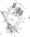
- FIG. 1 illustrates an embodiment of a stacked module arrangement 100.
- the stacked module arrangement 100 includes a first molded electronic module 102 and a second molded electronic module 104.
- the stacked module arrangement 100 may include more than two molded electronic modules 102, 104.
- the molded electronic modules 102, 104 may include components such as power devices like power transistors and/or power diodes, e.g., for switching a load current, inverting or converting a voltage, rectifying an alternating current, etc., logic devices such as a gate driver for a power transistor, a controller for a gate driver, etc., sensors, passive devices such as capacitors, inductors, transformers, etc. Still other types of devices used in power electronic applications may be included in the molded electronic modules 102, 104.
- the stacked module arrangement 100 also includes an interface by which the molded electronic modules 102, 104 are physically and electrically connected to one another in a stacked configuration.
- the interface is a press-fit interface that comprises press-fit connectors 106 protruding through a molded body 108 of the first molded electronic module 102 and received by corresponding openings 110 in a molded body 112 of the second molded electronic module 104.
- the molded bodies 108, 112 may be formed by placing the components of the respective electronic modules 102, 104 in a chamber and injecting liquified encapsulant material into the chamber. Examples of such techniques include injection molding, transfer molding, compression molding, and film-assist molding.
- the molded bodies 108, 112 may be formed by a lamination technique.
- the press-fit connectors 106 of the vertical (stacked) interface may be securely retained to a metal region of a substrate within the second molded electronic module 104 and enable an electrical connection with one or more semiconductor dies and/or passive components included in the second molded electronic module 104. At least some of the press-fit connectors 106 may extend through the molded body 112 of the second molded electronic module 104 to provide a connection interface at a side of the second molded electronic module facing away from the first molded electronic module 102, thereby enabling a press-fit connection between the stacked module arrangement 100 and a receiving apparatus such as a PCB (not shown in FIG. 1 ).
- the molded electronic modules 102, 104 may each have leads 114 protruding through the corresponding molded body 108, 112 for providing respective electrical interfaces to the molded electronic modules 102, 104.
- the first molded electronic module 102 is a power electronic module having a maximum breakdown voltage of at least 40V and a maximum DC current of at least 10A.
- the first molded electronic module 102 may have a maximum breakdown voltage of at least 80V and a DC operating current in a range of 10A to 400A.
- the first molded electronic module 102 may be used in 750V and/or 1200V applications, for example.
- the first molded electronic module 102 is a power module and not a logic or IC (integrated circuit) module.
- the second molded electronic module 104 may or may not be a power module.
- the second molded electronic module 104 may include passive components, sensors, a controller such as a microcontroller, electronic circuits, etc.
- the second molded electronic module 104 also is a power electronic module having a maximum breakdown voltage of at least 40V and a maximum DC current of at least 20A.
- the first and second molded electronic modules 102, 104 may form a power converter or inverter circuit.
- the first molded electronic module 102 may include a first half-bridge
- the second molded electronic module 104 may include a second half-bridge
- the first half-bridge and the second half-bridge may be stacked on one another via the vertical (stacked) interface of the stacked module arrangement 100, and the vertical (stacked) interface may enable a half bridge switching node connection between the power transistor modules.
- the module leads 114 may provide a ground connection as well as control and other signalling.
- the first molded electronic module 102 includes a power transistor die such as an IGBT (insulated gate bipolar transistor) die, a Si power MOSFET (metal-oxide semiconductor) die, a SiC power transistor die, a GaN HEMT (high-electron mobility transistor) die, etc.
- the second molded electronic module 104 includes a diode die, and the vertical (stacked) interface of the stacked module arrangement 100 electrically connects the diode die and the power transistor die in an anti-parallel configuration.
- the first molded electronic module 102 includes a power converter or inverter and the second molded electronic module 104 includes a controller for the power converter or inverter.
- the first molded electronic module 102 includes a power converter or inverter and the second molded electronic module 104 includes a rectifier and/or PFC (power factor correction) stage.
- the second molded electronic module 104 may include a totem pole type rectifier.
- the second molded electronic module 104 is a logic module that includes a controller and/or a gate driver for the first molded electronic module 102.
- the first molded electronic module 102 includes a rectifier and PFC stage and the second molded electronic module 104 includes an inverter or PFC only.
- one or both of the molded electronic modules 102, 104 may be part of a larger circuit, e.g., multilevel or even single switches composing a half-bridge with other stacked modules.
- One or both of the molded electronic modules 102, 104 may be implemented as a parallel connection of the same type of module.
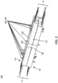
- FIG. 2 illustrates another embodiment of a stacked module arrangement 200.
- the embodiment illustrated in FIG. 2 is similar to the embodiment illustrated in FIG. 1 .
- one or more bus bars 202 are connected to a connection interface 204 formed by a part of the press-fit connectors 106 that extend through the molded body 112 of the second molded electronic module 104 at the opposite side as the first molded electronic module 102.
- Each bus bar 202 is a metallic strip or bar configured for high current power distribution.
- FIG. 3 illustrates another embodiment of a stacked module arrangement 300.
- the embodiment illustrated in FIG. 3 is similar to the embodiment illustrated in FIG. 1 .
- a circuit board 302 is connected to a connection interface 304 formed by the press-fit connectors 106 that extend through the molded body 112 of the second molded electronic module 104 at the opposite side as the first molded electronic module 102.
- the circuit board 302 may be a single-layer or multi-layer PCB, for example.
- the circuit board 302 may include metal traces 306, electronic devices 308 such as active and/or passive semiconductor dies, passive components 310 such as capacitors, inductors, etc.
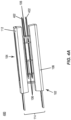
- FIG. 4A illustrates another embodiment of a stacked module arrangement 400.
- the embodiment illustrated in FIG. 4A is similar to the embodiment illustrated in FIG. 1 .
- at least one circuit board 402 is interposed between the first molded electronic module 102 and the second molded electronic module 104.
- At least some of the press-fit connectors 106 of the vertical (stacked) interface extend through the circuit board(s) 402 and into the molded body 112 of the second molded electronic module 104.
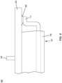
- FIG. 4B illustrates an enlarged view of one part of the stacked module arrangement 400.
- Each circuit board 402 may have metal traces 404 and other components one or both sides of the board 402.
- both the first molded electronic module 102 and the second molded electronic module 104 are power electronic modules each having a maximum breakdown voltage of at least 40V and a maximum DC current of at least 10A, and together form a power converter or inverter circuit where the circuit board 402 includes a gate driver and/or controller for the power electronic modules.
- FIG. 5 illustrates another embodiment of a stacked module arrangement 500.
- the embodiment illustrated in FIG. 5 is similar to the embodiment illustrated in FIG. 1 .
- the vertical (stacked) interface includes a solder joint 502 between at least some of the leads 114 of the molded electronic modules 102, 104.
- FIG. 6 illustrates another embodiment of a stacked module arrangement 600.
- the embodiment illustrated in FIG. 6 is similar to the embodiment illustrated in FIG. 5 .
- a solder joint 602 is formed between leads 114 of the first molded electronic module 102 and a bus bar 604.
- the second molded electronic module 104 is not shown in FIG. 6 but may be similarly soldered to the bus bar 604 at the opposite side as the first molded electronic module 102.
- the press-fit connectors 106 of the vertical (stacked) interface pass through openings (out of view) in the bus bar 604 and into the openings 110 formed in the molded body 112 of the second molded electronic module 104.
- both the first molded electronic module 102 and the second molded electronic module 104 are power electronic modules each having a maximum breakdown voltage of at least 40V and a maximum DC current of at least 10A, and together form a power converter or inverter circuit where the bus bar 604 carries a phase or load current or implements a +DC or -DC terminal of the power converter or inverter circuit.
- FIG. 7 illustrates another embodiment of a stacked module arrangement 700.
- the embodiment illustrated in FIG. 7 is similar to the embodiment illustrated in FIGS. 4A and 4B .
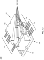
- at least one bus bar 702 is connected to the vertical (stacked) interface and interposed between the molded electronic modules 102, 104.
- At least some of the press-fit connectors 106 of the vertical (stacked) interface pass through openings 704 in each bus bar 702 and into the molded body 112 of the second molded electronic module 104.
- Other ones of the press-fit connectors 106 may be outside the region of the bus bar(s) 702 and pass directly into the molded body 112 of the second molded electronic module 104 without passing through a bus bar 702.
- both the first molded electronic module 102 and the second molded electronic module 104 are power electronic modules each having a maximum breakdown voltage of at least 40V and a maximum DC current of at least 10A, and together form a power converter or inverter circuit where each bus bar 702 carries a phase or load current or implements a +DC or -DC terminal of the power converter or inverter circuit.
- the outward facing side of each molded electronic module 102, 104 may have an exposed metal surface 706 which may be part of a metallized substrate, metal clip, leadframe, etc. embedded in the corresponding molded body 108, 112. In this case, enhanced cooling may be provided at this side of the molded electronic modules 102, 104.
- FIG. 8 illustrates another embodiment of a stacked module arrangement 800.
- the embodiment illustrated in FIG. 8 is similar to the embodiment illustrated in FIG. 1 .
- a first cooling device 802 is thermally coupled to a side 804 of the first molded electronic module 102 facing away from the vertical (stacked) interface.
- a second cooling device 806 is thermally coupled to a side 808 of the second molded electronic module 104 facing away from the vertical (stacked) interface.
- the cooling devices 802, 806 may be air-cooled or liquid-cooled heat sinks, for example.
- FIG. 9 illustrates another embodiment of a stacked module arrangement 900.
- the embodiment illustrated in FIG. 9 is similar to the embodiment illustrated in FIG. 8 .
- one or both cooling devices 802, 806 may include fins 902 for enhanced heat dissipation.
- FIG. 10 illustrates another embodiment of a stacked module arrangement 1000.
- the embodiment illustrated in FIG. 10 is similar to the embodiment illustrated in FIGS. 4A , 4B and 9 .
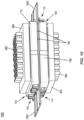
- a circuit board 1002 is interposed between the molded electronic modules 102, 104. At least some of the press-fit connectors 106 of the vertical (stacked) interface extend through the circuit board 1002 and into the molded body 112 of the second molded electronic module 104.
- the circuit board 1002 may have metal traces 1004 and other components one or both sides of the board 1002. In one embodiment, the circuit board 1002 provides power and control signals to one or both of the molded electronic modules 102, 104.
- FIG. 11 illustrates another embodiment of a stacked module arrangement 1100.
- the embodiment illustrated in FIG. 11 is similar to the embodiment illustrated in FIG. 1 .
- the second molded electronic module 104 is a logic module that includes a controller and/or a gate driver for the first molded electronic module 102.
- At least some of the press-fit connectors 106 of the vertical (stacked) interface may extend through the molded body 112 of the second molded electronic module 104 to provide a connection interface 1102 at a side of the second molded electronic module facing away from the first molded electronic module 102, thereby enabling a press-fit connection between the stacked module arrangement 1100 and a receiving apparatus such as a PCB (not shown in FIG. 11 ).
- Other ones of the press-fit connectors 106 may be outside the region of the second molded electronic module 104 and pass directly to the receiving apparatus as part of the connection interface 1102.
- FIG. 12 illustrates another embodiment of a stacked module arrangement 1200.
- the embodiment illustrated in FIG. 12 is similar to the embodiment illustrated in FIG. 1 .
- the first molded electronic module 102 overhangs the second molded electronic module 104 such that part of the second molded electronic module 104 is not covered by the first molded electronic module 102.
- At least some of the press-fit connectors 106 of the vertical (stacked) interface may extend through the molded body 108 of the first molded electronic module 102 to provide a connection interface 1202 at a side of the first molded electronic module facing away from the second molded electronic module 104, thereby enabling a press-fit connection between the stacked module arrangement 1200 and a receiving apparatus such as a PCB (not shown in FIG. 11 ).
- Other ones of the press-fit connectors 106 may be outside the region of the first molded electronic module 102 and pass directly to the receiving apparatus as part of the connection interface 1202.
- FIG. 13 illustrates another embodiment of a stacked module arrangement 1300.
- the embodiment illustrated in FIG. 13 is similar to the embodiment illustrated in FIG. 12 .
- a third molded electronic module 1302 physically and electrically connected to the second molded electronic module 104 in a stacked configuration via the same interface that physically and electrically connects the first molded electronic module 102 to the second molded electronic module 104 in the same stacked configuration.
- the third molded electronic module 1302 is disposed over the part of the second molded electronic module 104 not covered by the first molded electronic module 102 such that the first and third molded electronic modules 102, 1302 may be coplanar if the first and third molded electronic modules 104, 1302 are of the same module type.
- the third molded electronic module 1302 is a power electronic module having a maximum breakdown voltage of at least 40V and a maximum DC current of at least 10A and the vertical (stacked) interface physically and electrically connects the third molded electronic module 1302 and the second molded electronic module 104 to one another as part of the stacked configuration.
- the first molded electronic module 102 may include a single power switch die
- the third molded electronic module 1302 may include a single power switch die
- the single power switch die included in the first molded electronic module 102 and the single power switch die included in the third molded electronic module 1302 may be electrically connected in a half-bridge configuration by the vertical (stacked) interface
- the second molded electronic module 104 may be configured to drive both the single switch die included in the first molded electronic module 102 and the single switch die included in the third molded electronic module 1302.
- Example 1 A stacked module arrangement, comprising: a first molded electronic module; a second molded electronic module; and an interface by which the first molded electronic module and the second molded electronic module are physically and electrically connected to one another in a stacked configuration, wherein the first molded electronic module is a power electronic module having a maximum breakdown voltage of at least 40V and a maximum DC current of at least 10A.
- Example 2 The stacked module arrangement of example 1, wherein the interface is a press-fit interface that comprises a plurality of press-fit connectors protruding through a molded body of the first molded electronic module and received by a corresponding plurality of openings in a molded body of the second molded electronic module.
- Example 3 The stacked module arrangement of example 2, wherein at least some of the press-fit connectors extend through the molded body of the second molded electronic module to provide a connection interface at a side of the second molded electronic module facing away from the first molded electronic module.
- Example 4 The stacked module arrangement of example 3, further comprising one or more bus bars connected to the connection interface.
- Example 5 The stacked module arrangement of example 3 or 4, further comprising a circuit board connected to the connection interface.
- Example 6 The stacked module arrangement of any of examples 2 through 5, further comprising a circuit board interposed between the first molded electronic module and the second molded electronic module.
- Example 7 The stacked module arrangement of example 6, wherein at least some of the press-fit connectors extend through the circuit board and into a molded body of the second molded electronic module.
- Example 8 The stacked module arrangement of example 1, wherein the interface comprises a solder joint between leads of the first and molded electronic modules.
- Example 9 The stacked module arrangement of any of examples 1 through 8, wherein the second molded electronic module is a power electronic module having a maximum breakdown voltage of at least 40V and a maximum DC current of at least 10A, and wherein the first molded electronic module and the second molded electronic module form a power converter or inverter circuit.
- Example 10 The stacked module arrangement of example 9, further comprising a circuit board and/or a bus bar connected to the interface and interposed between the first molded electronic module and the second molded electronic module.
- Example 11 The stacked module arrangement of example 9 or 10, further comprising: a first cooling device thermally coupled to a side of the first molded electronic module facing away from the interface; and a second cooling device thermally coupled to a side of the second molded electronic module facing away from the interface.
- Example 12 The stacked module arrangement of any of examples 9 through 11, wherein the first molded electronic module includes a first half-bridge, wherein the second molded electronic module includes a second half-bridge, and wherein the first half-bridge and the second half-bridge are stacked on one another via the interface.
- Example 13 The stacked module arrangement of any of examples 1 through 12, wherein the first molded electronic module includes a transistor die, wherein the second molded electronic module includes a diode die, and wherein the interface electrically connects the diode die and the transistor die in an anti-parallel configuration.
- Example 14 The stacked module arrangement of any of examples 1 through 12, wherein the first molded electronic module includes a power converter or inverter, and wherein the second molded electronic module includes a controller for the power converter or inverter.
- Example 15 The stacked module arrangement of any of examples 1 through 12, wherein the first molded electronic module includes a power converter or inverter, and wherein the second molded electronic module includes a rectifier.
- Example 16 The stacked module arrangement of any of examples 1 through 12, wherein the second molded electronic module is a logic module that includes a controller and/or a gate driver for the first molded electronic module.
- Example 17 The stacked module arrangement of any pf examples 1 through 16, further comprising one or more circuit boards physically and electrically connected to the interface and interposed between the first molded electronic module and the second molded electronic module.
- Example 18 The stacked module arrangement of any of examples 1 through 17, further comprising one or more bus bars connected to the interface and interposed between the first molded electronic module and the second molded electronic module.
- Example 19 The stacked module arrangement of any of examples 1 through 18, further comprising a third molded electronic module, wherein the third molded electronic module is a power electronic module having a maximum breakdown voltage of at least 40V and a maximum DC current of at least 10A, and wherein the interface physically and electrically connects the third molded electronic module and the second molded electronic module to one another as part of the stacked configuration.
- the third molded electronic module is a power electronic module having a maximum breakdown voltage of at least 40V and a maximum DC current of at least 10A, and wherein the interface physically and electrically connects the third molded electronic module and the second molded electronic module to one another as part of the stacked configuration.
- Example 20 The stacked module arrangement of example 19, wherein the first molded electronic module includes a single power switch die, wherein the third molded electronic module includes a single power switch die, wherein the single power switch die included in the first molded electronic module and the single power switch die included in the third molded electronic module are electrically connected in a half-bridge configuration by the interface, and wherein the second molded electronic module is configured to drive both the single switch die included in the first molded electronic module and the single switch die included in the third molded electronic module.
- Example 21 The stacked module arrangement of any of examples 1 through 20, wherein the maximum breakdown voltage is in a range of 750V to 1200V.
Landscapes
- Engineering & Computer Science (AREA)
- Microelectronics & Electronic Packaging (AREA)
- Inverter Devices (AREA)
- Rectifiers (AREA)
Abstract
Description
- Molded power semiconductor modules are used in a wide range of power electronic applications, including inverters, converters, rectifiers, motor control, etc. Parallel connection of two or more molded modules increases the x/y (lateral) dimensions on the system PCB (printed circuit board). Several molded modules or packages are soldered/placed on a PCB to realize power electronic systems, increasing the PCB size. Side-by-side arrangement of molded modules may allow for enhanced cooling. However, enhanced cooling may not be required or possible for some applications. For example, power electronic arrangement in a washing machine or airplane application do not require or cannot accommodate enhanced cooling. In applications where enhanced cooling is not required or cannot be accommodated, a side-by-side arrangement of molded modules results in an unnecessary increase in PCB size which increases overall system cost.
- Accordingly, there is a need for a more efficient molded power semiconductor module arrangement for applications that do not require or cannot accommodate enhanced cooling afforded by a side-by-side module arrangement.
- According to an embodiment of a stacked module arrangement, the stacked module arrangement comprises: a first molded electronic module; a second molded electronic module; and an interface by which the first molded electronic module and the second molded electronic module are physically and electrically connected to one another in a stacked configuration, wherein the first molded electronic module is a power electronic module having a maximum breakdown voltage of at least 40V and a maximum DC current of at least 10A.
- Those skilled in the art will recognize additional features and advantages upon reading the following detailed description, and upon viewing the accompanying drawings.
- The elements of the drawings are not necessarily to scale relative to each other. Like reference numerals designate corresponding similar parts. The features of the various illustrated embodiments can be combined unless they exclude each other. Embodiments are depicted in the drawings and are detailed in the description which follows.
-
FIG. 1 illustrates a side perspective view of an embodiment of a stacked module arrangement. -
FIG. 2 illustrates a side perspective view of another embodiment of a stacked module arrangement. -
FIG. 3 illustrates a top perspective view of another embodiment of a stacked module arrangement. -
FIG. 4A illustrates a side perspective view of another embodiment of a stacked module arrangement. -
FIG. 4B illustrates an enlarged view of one part of the stacked module arrangement shown inFIG. 4A . -
FIG. 5 illustrates a partial side view of another embodiment of a stacked module arrangement. -
FIG. 6 illustrates a partial side view of another embodiment of a stacked module arrangement. -
FIG. 7 illustrates a top perspective view of another embodiment of a stacked module arrangement. -
FIG. 8 illustrates a side view of another embodiment of a stacked module arrangement. -
FIG. 9 illustrates a top perspective view of another embodiment of a stacked module arrangement. -
FIG. 10 illustrates a side perspective view of another embodiment of a stacked module arrangement. -
FIG. 11 illustrates a top perspective view of another embodiment of a stacked module arrangement. -
FIG. 12 illustrates a top perspective view of another embodiment of a stacked module arrangement. -
FIG. 13 illustrates a top perspective view of another embodiment of a stacked module arrangement. - The embodiments described herein provide a stacked arrangement of molded electronic modules that occupies less board space compared to a side-by-side module arrangement. Two or more molded electronic modules may be stacked on one another in a vertical arrangement such that the x/y (lateral) dimensions of the system board to which the stacked module arrangement is attached do not need to be increased to accommodate the molded electronic modules. The board may be attached to either side of the stacked module arrangement or interposed between two molded electronic modules included in the stacked module arrangement. In other applications, the board may be omitted or more than one board may be used.
- The molded electronic modules included in the stacked module arrangement may include components such as power devices like power transistors and/or power diodes, e.g., for switching a load current, inverting or converting a voltage, rectifying an alternating current, etc., logic devices such as a gate driver for a power transistor, a controller for a gate driver, etc., sensors, passive devices such as capacitors, inductors, transformers, etc. Still other types of devices used in power electronic applications may be included in the molded electronic modules. In each case, the molded electronic modules are physically and electrically connected to one another in a stacked configuration via an interface and at least one of the molded electronic modules is a power electronic module having a maximum breakdown voltage of at least 40V and a maximum DC current of at least 10A.
- Described next, with reference to the figures, are exemplary embodiments of the stacked module arrangement.
-
FIG. 1 illustrates an embodiment of a stackedmodule arrangement 100. Thestacked module arrangement 100 includes a first moldedelectronic module 102 and a second moldedelectronic module 104. The stackedmodule arrangement 100 may include more than two moldedelectronic modules electronic modules electronic modules - The stacked
module arrangement 100 also includes an interface by which the moldedelectronic modules FIG. 1 , the interface is a press-fit interface that comprises press-fit connectors 106 protruding through a moldedbody 108 of the first moldedelectronic module 102 and received bycorresponding openings 110 in a moldedbody 112 of the second moldedelectronic module 104. Themolded bodies electronic modules molded bodies - The press-
fit connectors 106 of the vertical (stacked) interface may be securely retained to a metal region of a substrate within the second moldedelectronic module 104 and enable an electrical connection with one or more semiconductor dies and/or passive components included in the second moldedelectronic module 104. At least some of the press-fit connectors 106 may extend through themolded body 112 of the second moldedelectronic module 104 to provide a connection interface at a side of the second molded electronic module facing away from the first moldedelectronic module 102, thereby enabling a press-fit connection between the stackedmodule arrangement 100 and a receiving apparatus such as a PCB (not shown inFIG. 1 ). The moldedelectronic modules molded body electronic modules - According to the embodiment illustrated in
FIG. 1 , the first moldedelectronic module 102 is a power electronic module having a maximum breakdown voltage of at least 40V and a maximum DC current of at least 10A. For example, the first moldedelectronic module 102 may have a maximum breakdown voltage of at least 80V and a DC operating current in a range of 10A to 400A. The first moldedelectronic module 102 may be used in 750V and/or 1200V applications, for example. In each case, the first moldedelectronic module 102 is a power module and not a logic or IC (integrated circuit) module. The second moldedelectronic module 104 may or may not be a power module. For example, the second moldedelectronic module 104 may include passive components, sensors, a controller such as a microcontroller, electronic circuits, etc. - In one embodiment, the second molded
electronic module 104 also is a power electronic module having a maximum breakdown voltage of at least 40V and a maximum DC current of at least 20A. According to this embodiment, the first and second moldedelectronic modules electronic module 102 may include a first half-bridge, the second moldedelectronic module 104 may include a second half-bridge, the first half-bridge and the second half-bridge may be stacked on one another via the vertical (stacked) interface of thestacked module arrangement 100, and the vertical (stacked) interface may enable a half bridge switching node connection between the power transistor modules. The module leads 114 may provide a ground connection as well as control and other signalling. - In another embodiment, the first molded
electronic module 102 includes a power transistor die such as an IGBT (insulated gate bipolar transistor) die, a Si power MOSFET (metal-oxide semiconductor) die, a SiC power transistor die, a GaN HEMT (high-electron mobility transistor) die, etc., the second moldedelectronic module 104 includes a diode die, and the vertical (stacked) interface of the stackedmodule arrangement 100 electrically connects the diode die and the power transistor die in an anti-parallel configuration. - In another embodiment, the first molded
electronic module 102 includes a power converter or inverter and the second moldedelectronic module 104 includes a controller for the power converter or inverter. - In another embodiment, the first molded
electronic module 102 includes a power converter or inverter and the second moldedelectronic module 104 includes a rectifier and/or PFC (power factor correction) stage. For example, the second moldedelectronic module 104 may include a totem pole type rectifier. - In another embodiment, the second molded
electronic module 104 is a logic module that includes a controller and/or a gate driver for the first moldedelectronic module 102. - In another embodiment, the first molded
electronic module 102 includes a rectifier and PFC stage and the second moldedelectronic module 104 includes an inverter or PFC only. - In general, one or both of the molded
electronic modules electronic modules -
FIG. 2 illustrates another embodiment of a stackedmodule arrangement 200. The embodiment illustrated inFIG. 2 is similar to the embodiment illustrated inFIG. 1 . InFIG. 2 , one ormore bus bars 202 are connected to a connection interface 204 formed by a part of the press-fit connectors 106 that extend through the moldedbody 112 of the second moldedelectronic module 104 at the opposite side as the first moldedelectronic module 102. Eachbus bar 202 is a metallic strip or bar configured for high current power distribution. -
FIG. 3 illustrates another embodiment of a stackedmodule arrangement 300. The embodiment illustrated inFIG. 3 is similar to the embodiment illustrated inFIG. 1 . InFIG. 3 , acircuit board 302 is connected to a connection interface 304 formed by the press-fit connectors 106 that extend through the moldedbody 112 of the second moldedelectronic module 104 at the opposite side as the first moldedelectronic module 102. Thecircuit board 302 may be a single-layer or multi-layer PCB, for example. Thecircuit board 302 may include metal traces 306,electronic devices 308 such as active and/or passive semiconductor dies,passive components 310 such as capacitors, inductors, etc. -
FIG. 4A illustrates another embodiment of a stackedmodule arrangement 400. The embodiment illustrated inFIG. 4A is similar to the embodiment illustrated inFIG. 1 . InFIG. 4A , at least onecircuit board 402 is interposed between the first moldedelectronic module 102 and the second moldedelectronic module 104. At least some of the press-fit connectors 106 of the vertical (stacked) interface extend through the circuit board(s) 402 and into the moldedbody 112 of the second moldedelectronic module 104.FIG. 4B illustrates an enlarged view of one part of the stackedmodule arrangement 400. Eachcircuit board 402 may have metal traces 404 and other components one or both sides of theboard 402. In one embodiment, both the first moldedelectronic module 102 and the second moldedelectronic module 104 are power electronic modules each having a maximum breakdown voltage of at least 40V and a maximum DC current of at least 10A, and together form a power converter or inverter circuit where thecircuit board 402 includes a gate driver and/or controller for the power electronic modules. -
FIG. 5 illustrates another embodiment of a stackedmodule arrangement 500. The embodiment illustrated inFIG. 5 is similar to the embodiment illustrated inFIG. 1 . InFIG. 5 , the vertical (stacked) interface includes a solder joint 502 between at least some of theleads 114 of the moldedelectronic modules -
FIG. 6 illustrates another embodiment of a stackedmodule arrangement 600. The embodiment illustrated inFIG. 6 is similar to the embodiment illustrated inFIG. 5 . InFIG. 6 , asolder joint 602 is formed betweenleads 114 of the first moldedelectronic module 102 and abus bar 604. The second moldedelectronic module 104 is not shown inFIG. 6 but may be similarly soldered to thebus bar 604 at the opposite side as the first moldedelectronic module 102. The press-fit connectors 106 of the vertical (stacked) interface pass through openings (out of view) in thebus bar 604 and into theopenings 110 formed in the moldedbody 112 of the second moldedelectronic module 104. In one embodiment, both the first moldedelectronic module 102 and the second moldedelectronic module 104 are power electronic modules each having a maximum breakdown voltage of at least 40V and a maximum DC current of at least 10A, and together form a power converter or inverter circuit where thebus bar 604 carries a phase or load current or implements a +DC or -DC terminal of the power converter or inverter circuit. -
FIG. 7 illustrates another embodiment of a stackedmodule arrangement 700. The embodiment illustrated inFIG. 7 is similar to the embodiment illustrated inFIGS. 4A and4B . InFIG. 7 , at least onebus bar 702 is connected to the vertical (stacked) interface and interposed between the moldedelectronic modules fit connectors 106 of the vertical (stacked) interface pass throughopenings 704 in eachbus bar 702 and into the moldedbody 112 of the second moldedelectronic module 104. Other ones of the press-fit connectors 106 may be outside the region of the bus bar(s) 702 and pass directly into the moldedbody 112 of the second moldedelectronic module 104 without passing through abus bar 702. - In one embodiment, both the first molded
electronic module 102 and the second moldedelectronic module 104 are power electronic modules each having a maximum breakdown voltage of at least 40V and a maximum DC current of at least 10A, and together form a power converter or inverter circuit where eachbus bar 702 carries a phase or load current or implements a +DC or -DC terminal of the power converter or inverter circuit. As shown inFIG. 7 , the outward facing side of each moldedelectronic module metal surface 706 which may be part of a metallized substrate, metal clip, leadframe, etc. embedded in the corresponding moldedbody electronic modules -
FIG. 8 illustrates another embodiment of a stackedmodule arrangement 800. The embodiment illustrated inFIG. 8 is similar to the embodiment illustrated inFIG. 1 . InFIG. 8 , afirst cooling device 802 is thermally coupled to aside 804 of the first moldedelectronic module 102 facing away from the vertical (stacked) interface. Asecond cooling device 806 is thermally coupled to aside 808 of the second moldedelectronic module 104 facing away from the vertical (stacked) interface. Thecooling devices -
FIG. 9 illustrates another embodiment of a stackedmodule arrangement 900. The embodiment illustrated inFIG. 9 is similar to the embodiment illustrated inFIG. 8 . InFIG. 9 , one or both coolingdevices fins 902 for enhanced heat dissipation. -
FIG. 10 illustrates another embodiment of a stackedmodule arrangement 1000. The embodiment illustrated inFIG. 10 is similar to the embodiment illustrated inFIGS. 4A ,4B and9 . InFIG. 10 , acircuit board 1002 is interposed between the moldedelectronic modules fit connectors 106 of the vertical (stacked) interface extend through thecircuit board 1002 and into the moldedbody 112 of the second moldedelectronic module 104. Thecircuit board 1002 may havemetal traces 1004 and other components one or both sides of theboard 1002. In one embodiment, thecircuit board 1002 provides power and control signals to one or both of the moldedelectronic modules -
FIG. 11 illustrates another embodiment of a stackedmodule arrangement 1100. The embodiment illustrated inFIG. 11 is similar to the embodiment illustrated inFIG. 1 . InFIG. 11 , the second moldedelectronic module 104 is a logic module that includes a controller and/or a gate driver for the first moldedelectronic module 102. At least some of the press-fit connectors 106 of the vertical (stacked) interface may extend through the moldedbody 112 of the second moldedelectronic module 104 to provide a connection interface 1102 at a side of the second molded electronic module facing away from the first moldedelectronic module 102, thereby enabling a press-fit connection between thestacked module arrangement 1100 and a receiving apparatus such as a PCB (not shown inFIG. 11 ). Other ones of the press-fit connectors 106 may be outside the region of the second moldedelectronic module 104 and pass directly to the receiving apparatus as part of the connection interface 1102. -
FIG. 12 illustrates another embodiment of a stackedmodule arrangement 1200. The embodiment illustrated inFIG. 12 is similar to the embodiment illustrated inFIG. 1 . InFIG. 12 , the first moldedelectronic module 102 overhangs the second moldedelectronic module 104 such that part of the second moldedelectronic module 104 is not covered by the first moldedelectronic module 102. At least some of the press-fit connectors 106 of the vertical (stacked) interface may extend through the moldedbody 108 of the first moldedelectronic module 102 to provide a connection interface 1202 at a side of the first molded electronic module facing away from the second moldedelectronic module 104, thereby enabling a press-fit connection between thestacked module arrangement 1200 and a receiving apparatus such as a PCB (not shown inFIG. 11 ). Other ones of the press-fit connectors 106 may be outside the region of the first moldedelectronic module 102 and pass directly to the receiving apparatus as part of the connection interface 1202. -
FIG. 13 illustrates another embodiment of a stackedmodule arrangement 1300. The embodiment illustrated inFIG. 13 is similar to the embodiment illustrated inFIG. 12 . InFIG. 13 , a third moldedelectronic module 1302 physically and electrically connected to the second moldedelectronic module 104 in a stacked configuration via the same interface that physically and electrically connects the first moldedelectronic module 102 to the second moldedelectronic module 104 in the same stacked configuration. The third moldedelectronic module 1302 is disposed over the part of the second moldedelectronic module 104 not covered by the first moldedelectronic module 102 such that the first and third moldedelectronic modules electronic modules - In one embodiment, the third molded
electronic module 1302 is a power electronic module having a maximum breakdown voltage of at least 40V and a maximum DC current of at least 10A and the vertical (stacked) interface physically and electrically connects the third moldedelectronic module 1302 and the second moldedelectronic module 104 to one another as part of the stacked configuration. For example, the first moldedelectronic module 102 may include a single power switch die, the third moldedelectronic module 1302 may include a single power switch die, the single power switch die included in the first moldedelectronic module 102 and the single power switch die included in the third moldedelectronic module 1302 may be electrically connected in a half-bridge configuration by the vertical (stacked) interface, and the second moldedelectronic module 104 may be configured to drive both the single switch die included in the first moldedelectronic module 102 and the single switch die included in the third moldedelectronic module 1302. - Although the present disclosure is not so limited, the following numbered examples demonstrate one or more aspects of the disclosure.
- Example 1. A stacked module arrangement, comprising: a first molded electronic module; a second molded electronic module; and an interface by which the first molded electronic module and the second molded electronic module are physically and electrically connected to one another in a stacked configuration, wherein the first molded electronic module is a power electronic module having a maximum breakdown voltage of at least 40V and a maximum DC current of at least 10A.
- Example 2. The stacked module arrangement of example 1, wherein the interface is a press-fit interface that comprises a plurality of press-fit connectors protruding through a molded body of the first molded electronic module and received by a corresponding plurality of openings in a molded body of the second molded electronic module.
- Example 3. The stacked module arrangement of example 2, wherein at least some of the press-fit connectors extend through the molded body of the second molded electronic module to provide a connection interface at a side of the second molded electronic module facing away from the first molded electronic module.
- Example 4. The stacked module arrangement of example 3, further comprising one or more bus bars connected to the connection interface.
- Example 5. The stacked module arrangement of example 3 or 4, further comprising a circuit board connected to the connection interface.
- Example 6. The stacked module arrangement of any of examples 2 through 5, further comprising a circuit board interposed between the first molded electronic module and the second molded electronic module.
- Example 7. The stacked module arrangement of example 6, wherein at least some of the press-fit connectors extend through the circuit board and into a molded body of the second molded electronic module.
- Example 8. The stacked module arrangement of example 1, wherein the interface comprises a solder joint between leads of the first and molded electronic modules.
- Example 9. The stacked module arrangement of any of examples 1 through 8, wherein the second molded electronic module is a power electronic module having a maximum breakdown voltage of at least 40V and a maximum DC current of at least 10A, and wherein the first molded electronic module and the second molded electronic module form a power converter or inverter circuit.
- Example 10. The stacked module arrangement of example 9, further comprising a circuit board and/or a bus bar connected to the interface and interposed between the first molded electronic module and the second molded electronic module.
- Example 11. The stacked module arrangement of example 9 or 10, further comprising: a first cooling device thermally coupled to a side of the first molded electronic module facing away from the interface; and a second cooling device thermally coupled to a side of the second molded electronic module facing away from the interface.
- Example 12. The stacked module arrangement of any of examples 9 through 11, wherein the first molded electronic module includes a first half-bridge, wherein the second molded electronic module includes a second half-bridge, and wherein the first half-bridge and the second half-bridge are stacked on one another via the interface.
- Example 13. The stacked module arrangement of any of examples 1 through 12, wherein the first molded electronic module includes a transistor die, wherein the second molded electronic module includes a diode die, and wherein the interface electrically connects the diode die and the transistor die in an anti-parallel configuration.
- Example 14. The stacked module arrangement of any of examples 1 through 12, wherein the first molded electronic module includes a power converter or inverter, and wherein the second molded electronic module includes a controller for the power converter or inverter.
- Example 15. The stacked module arrangement of any of examples 1 through 12, wherein the first molded electronic module includes a power converter or inverter, and wherein the second molded electronic module includes a rectifier.
- Example 16. The stacked module arrangement of any of examples 1 through 12, wherein the second molded electronic module is a logic module that includes a controller and/or a gate driver for the first molded electronic module.
- Example 17. The stacked module arrangement of any pf examples 1 through 16, further comprising one or more circuit boards physically and electrically connected to the interface and interposed between the first molded electronic module and the second molded electronic module.
- Example 18. The stacked module arrangement of any of examples 1 through 17, further comprising one or more bus bars connected to the interface and interposed between the first molded electronic module and the second molded electronic module.
- Example 19. The stacked module arrangement of any of examples 1 through 18, further comprising a third molded electronic module, wherein the third molded electronic module is a power electronic module having a maximum breakdown voltage of at least 40V and a maximum DC current of at least 10A, and wherein the interface physically and electrically connects the third molded electronic module and the second molded electronic module to one another as part of the stacked configuration.
- Example 20. The stacked module arrangement of example 19, wherein the first molded electronic module includes a single power switch die, wherein the third molded electronic module includes a single power switch die, wherein the single power switch die included in the first molded electronic module and the single power switch die included in the third molded electronic module are electrically connected in a half-bridge configuration by the interface, and wherein the second molded electronic module is configured to drive both the single switch die included in the first molded electronic module and the single switch die included in the third molded electronic module.
- Example 21. The stacked module arrangement of any of examples 1 through 20, wherein the maximum breakdown voltage is in a range of 750V to 1200V.
- Terms such as "first", "second", and the like, are used to describe various elements, regions, sections, etc. and are also not intended to be limiting. Like terms refer to like elements throughout the description.
- As used herein, the terms "having", "containing", "including", "comprising" and the like are open ended terms that indicate the presence of stated elements or features, but do not preclude additional elements or features. The articles "a", "an" and "the" are intended to include the plural as well as the singular, unless the context clearly indicates otherwise.
- It is to be understood that the features of the various embodiments described herein may be combined with each other, unless specifically noted otherwise.
- Although specific embodiments have been illustrated and described herein, it will be appreciated by those of ordinary skill in the art that a variety of alternate and/or equivalent implementations may be substituted for the specific embodiments shown and described without departing from the scope of the present invention. This application is intended to cover any adaptations or variations of the specific embodiments discussed herein. Therefore, it is intended that this invention be limited only by the claims and the equivalents thereof.
Claims (21)
- A stacked module arrangement, comprising:a first molded electronic module;a second molded electronic module; andan interface by which the first molded electronic module and the second molded electronic module are physically and electrically connected to one another in a stacked configuration, wherein the first molded electronic module is a power electronic module having a maximum breakdown voltage of at least 40V and a maximum DC current of at least 10A.
- The stacked module arrangement of claim 1, wherein the interface is a press-fit interface that comprises a plurality of press-fit connectors protruding through a molded body of the first molded electronic module and received by a corresponding plurality of openings in a molded body of the second molded electronic module.
- The stacked module arrangement of claim 2, wherein at least some of the press-fit connectors extend through the molded body of the second molded electronic module to provide a connection interface at a side of the second molded electronic module facing away from the first molded electronic module.
- The stacked module arrangement of claim 3, further comprising one or more bus bars connected to the connection interface.
- The stacked module arrangement of claim 3, further comprising a circuit board connected to the connection interface.
- The stacked module arrangement of claim 2, further comprising a circuit board interposed between the first molded electronic module and the second molded electronic module.
- The stacked module arrangement of claim 6, wherein at least some of the press-fit connectors extend through the circuit board and into a molded body of the second molded electronic module.
- The stacked module arrangement of any one of the preceding claims, wherein the interface comprises a solder joint between leads of the first and molded electronic modules.
- The stacked module arrangement of any one of the preceding claims, wherein the second molded electronic module is a power electronic module having a maximum breakdown voltage of at least 40V and a maximum DC current of at least 10A, and wherein the first molded electronic module and the second molded electronic module form a power converter or inverter circuit.
- The stacked module arrangement of claim 9, further comprising a circuit board and/or a bus bar connected to the interface and interposed between the first molded electronic module and the second molded electronic module.
- The stacked module arrangement of claim 9 or 10, further comprising:a first cooling device thermally coupled to a side of the first molded electronic module facing away from the interface; anda second cooling device thermally coupled to a side of the second molded electronic module facing away from the interface.
- The stacked module arrangement of any one of claims 9 to 11, wherein the first molded electronic module includes a first half-bridge, wherein the second molded electronic module includes a second half-bridge, and wherein the first half-bridge and the second half-bridge are stacked on one another via the interface.
- The stacked module arrangement of any one of the preceding claims, wherein the first molded electronic module includes a transistor die, wherein the second molded electronic module includes a diode die, and wherein the interface electrically connects the diode die and the transistor die in an anti-parallel configuration.
- The stacked module arrangement of any one of the preceding claims, wherein the first molded electronic module includes a power converter or inverter, and wherein the second molded electronic module includes a controller for the power converter or inverter.
- The stacked module arrangement of any one of the preceding claims, wherein the first molded electronic module includes a power converter or inverter, and wherein the second molded electronic module includes a rectifier.
- The stacked module arrangement of any one of the preceding claims, wherein the second molded electronic module is a logic module that includes a controller and/or a gate driver for the first molded electronic module.
- The stacked module arrangement of any one of the preceding claims, further comprising one or more circuit boards physically and electrically connected to the interface and interposed between the first molded electronic module and the second molded electronic module.
- The stacked module arrangement of any one of the preceding claims, further comprising one or more bus bars connected to the interface and interposed between the first molded electronic module and the second molded electronic module.
- The stacked module arrangement of any one of the preceding claims, further comprising a third molded electronic module, wherein the third molded electronic module is a power electronic module having a maximum breakdown voltage of at least 40V and a maximum DC current of at least 10A, and wherein the interface physically and electrically connects the third molded electronic module and the second molded electronic module to one another as part of the stacked configuration.
- The stacked module arrangement of claim 19, wherein the first molded electronic module includes a single power switch die, wherein the third molded electronic module includes a single power switch die, wherein the single power switch die included in the first molded electronic module and the single power switch die included in the third molded electronic module are electrically connected in a half-bridge configuration by the interface, and wherein the second molded electronic module is configured to drive both the single switch die included in the first molded electronic module and the single switch die included in the third molded electronic module.
- The stacked module arrangement of any one of the preceding claims, wherein the maximum breakdown voltage is in a range of 750V to 1200V.
Applications Claiming Priority (1)
| Application Number | Priority Date | Filing Date | Title |
|---|---|---|---|
| US17/577,879 US12438068B2 (en) | 2022-01-18 | 2022-01-18 | Stacked module arrangement |
Publications (2)
| Publication Number | Publication Date |
|---|---|
| EP4213208A2 true EP4213208A2 (en) | 2023-07-19 |
| EP4213208A3 EP4213208A3 (en) | 2023-12-13 |
Family
ID=84980928
Family Applications (1)
| Application Number | Title | Priority Date | Filing Date |
|---|---|---|---|
| EP23151388.8A Pending EP4213208A3 (en) | 2022-01-18 | 2023-01-12 | Stacked module arrangement |
Country Status (3)
| Country | Link |
|---|---|
| US (1) | US12438068B2 (en) |
| EP (1) | EP4213208A3 (en) |
| CN (1) | CN116471741A (en) |
Family Cites Families (44)
| Publication number | Priority date | Publication date | Assignee | Title |
|---|---|---|---|---|
| US5502333A (en) * | 1994-03-30 | 1996-03-26 | International Business Machines Corporation | Semiconductor stack structures and fabrication/sparing methods utilizing programmable spare circuit |
| KR100447035B1 (en) * | 1996-11-21 | 2004-09-07 | 가부시키가이샤 히타치세이사쿠쇼 | Manufacturing process of semiconductor device |
| KR100280398B1 (en) * | 1997-09-12 | 2001-02-01 | 김영환 | Manufacturing method of stacked semiconductor package module |
| US6297548B1 (en) * | 1998-06-30 | 2001-10-02 | Micron Technology, Inc. | Stackable ceramic FBGA for high thermal applications |
| SG111069A1 (en) * | 2002-06-18 | 2005-05-30 | Micron Technology Inc | Semiconductor devices including peripherally located bond pads, assemblies, packages, and methods |
| US7491897B2 (en) | 2002-09-30 | 2009-02-17 | Fujitsu Ten Limited | Electronic equipment provided with wiring board into which press-fit terminals are press-fitted |
| TWI231023B (en) * | 2003-05-27 | 2005-04-11 | Ind Tech Res Inst | Electronic packaging with three-dimensional stack and assembling method thereof |
| US6933593B2 (en) | 2003-08-14 | 2005-08-23 | International Rectifier Corporation | Power module having a heat sink |
| US7298027B2 (en) | 2004-09-02 | 2007-11-20 | International Rectifier Corporation | SMT three phase inverter package and lead frame |
| CN100539135C (en) * | 2004-09-08 | 2009-09-09 | 松下电器产业株式会社 | Three-dimensional circuit device, electronic equipment using the same, and manufacturing method thereof |
| DE102006032436A1 (en) | 2006-07-13 | 2008-01-17 | Siemens Ag | Device for arrangement of electronic element on printed circuit board, has support element, electro-technical element, which is arranged on support element, and cover that is provided with electro-technical element for support element |
| DE102006056363B4 (en) * | 2006-11-29 | 2010-12-09 | Infineon Technologies Ag | Semiconductor module with at least two substrates and method for producing a semiconductor module with two substrates |
| JP5252819B2 (en) | 2007-03-26 | 2013-07-31 | 三菱電機株式会社 | Semiconductor device and manufacturing method thereof |
| TWI402952B (en) * | 2007-09-27 | 2013-07-21 | 三洋電機股份有限公司 | Circuit device and method of manufacturing same |
| WO2009069308A1 (en) * | 2007-11-30 | 2009-06-04 | Panasonic Corporation | Heat dissipating structure base board, module using heat dissipating structure base board, and method for manufacturing heat dissipating structure base board |
| US7791177B2 (en) | 2007-12-10 | 2010-09-07 | Infineon Technologies Ag | Electronic device |
| JP2010021306A (en) * | 2008-07-10 | 2010-01-28 | Hitachi Ltd | Semiconductor device |
| JP4634497B2 (en) | 2008-11-25 | 2011-02-16 | 三菱電機株式会社 | Power semiconductor module |
| US8194411B2 (en) * | 2009-03-31 | 2012-06-05 | Hong Kong Applied Science and Technology Research Institute Co. Ltd | Electronic package with stacked modules with channels passing through metal layers of the modules |
| CN102340233B (en) | 2010-07-15 | 2014-05-07 | 台达电子工业股份有限公司 | Power module |
| JP5599328B2 (en) | 2011-01-20 | 2014-10-01 | 三菱電機株式会社 | Connection mechanism between power semiconductor device and printed wiring board |
| US8643188B2 (en) | 2011-06-03 | 2014-02-04 | Infineon Technologies Ag | Connecting system for electrically connecting electronic devices and method for connecting an electrically conductive first connector and electrically conductive second connector |
| EP2538761B1 (en) | 2011-06-20 | 2014-01-29 | STMicroelectronics Srl | Intelligent Power Module and related assembling method |
| JP5953790B2 (en) | 2011-10-12 | 2016-07-20 | 富士電機株式会社 | Semiconductor device and manufacturing method of semiconductor device |
| JP6475918B2 (en) | 2014-02-05 | 2019-02-27 | ローム株式会社 | Power module |
| JP6249892B2 (en) | 2014-06-27 | 2017-12-20 | 三菱電機株式会社 | Manufacturing method of semiconductor device |
| DE102014110967B4 (en) | 2014-08-01 | 2021-06-24 | Infineon Technologies Ag | Encapsulated electronic chip device with fastening device and externally accessible electrical connection structure and method for the production thereof |
| US9768087B2 (en) * | 2014-10-08 | 2017-09-19 | Infineon Technologies Americas Corp. | Compact high-voltage semiconductor package |
| KR20160049786A (en) | 2014-10-28 | 2016-05-10 | 현대모비스 주식회사 | Power module and pakaking method thereof |
| JP6459418B2 (en) | 2014-11-13 | 2019-01-30 | 富士電機株式会社 | Semiconductor device and manufacturing method thereof |
| JP6288301B2 (en) | 2014-11-28 | 2018-03-14 | 日産自動車株式会社 | Half-bridge power semiconductor module and manufacturing method thereof |
| JP6316504B2 (en) | 2015-05-21 | 2018-04-25 | 三菱電機株式会社 | Power semiconductor device |
| US10431847B2 (en) * | 2016-09-19 | 2019-10-01 | International Business Machines Corporation | Stacked film battery architecture |
| JP6843731B2 (en) * | 2017-11-22 | 2021-03-17 | 三菱電機株式会社 | Semiconductor device |
| JP7010036B2 (en) | 2018-02-07 | 2022-01-26 | 株式会社デンソー | Semiconductor module |
| US10304788B1 (en) | 2018-04-11 | 2019-05-28 | Semiconductor Components Industries, Llc | Semiconductor power module to protect against short circuit event |
| US10790220B2 (en) | 2018-10-18 | 2020-09-29 | Nxp B.V. | Press-fit semiconductor device |
| US20210202439A1 (en) | 2019-12-26 | 2021-07-01 | Industrial Technology Research Institute | High power module |
| JP7542058B2 (en) | 2020-04-24 | 2024-08-29 | 日産自動車株式会社 | Electronic Control Module |
| US11682611B2 (en) | 2020-06-22 | 2023-06-20 | Infineon Technologies Ag | Power semiconductor module |
| US11652078B2 (en) | 2021-04-20 | 2023-05-16 | Infineon Technologies Ag | High voltage semiconductor package with pin fit leads |
| US11901273B2 (en) | 2021-07-26 | 2024-02-13 | Infineon Technologies Ag | Power module with press-fit contacts |
| US12494418B2 (en) | 2021-07-26 | 2025-12-09 | Infineon Technologies Ag | Power module with press-fit contacts |
| US12610829B2 (en) | 2023-05-31 | 2026-04-21 | Semiconductor Components Industries, Llc | Power module package with molded via and dual side press-fit pin |
-
2022
- 2022-01-18 US US17/577,879 patent/US12438068B2/en active Active
-
2023
- 2023-01-12 EP EP23151388.8A patent/EP4213208A3/en active Pending
- 2023-01-17 CN CN202310079794.4A patent/CN116471741A/en active Pending
Also Published As
| Publication number | Publication date |
|---|---|
| US12438068B2 (en) | 2025-10-07 |
| EP4213208A3 (en) | 2023-12-13 |
| US20230230905A1 (en) | 2023-07-20 |
| CN116471741A (en) | 2023-07-21 |
Similar Documents
| Publication | Publication Date | Title |
|---|---|---|
| CN110785842B (en) | Half-bridge module with coaxial arrangement of DC terminals | |
| US8987777B2 (en) | Stacked half-bridge power module | |
| US9865529B2 (en) | Semiconductor module with conductive pin | |
| US9888563B2 (en) | Electronics assembly with interference-suppression capacitors | |
| US10130015B2 (en) | Electronic circuit unit | |
| US8514579B2 (en) | Power semiconductor module including substrates spaced from each other | |
| US8115294B2 (en) | Multichip module with improved system carrier | |
| US11527456B2 (en) | Power module with organic layers | |
| US9653386B2 (en) | Compact multi-die power semiconductor package | |
| US20190237416A1 (en) | Power device package | |
| US9196510B2 (en) | Semiconductor package comprising two semiconductor modules and laterally extending connectors | |
| US9468087B1 (en) | Power module with improved cooling and method for making | |
| EP2871676B1 (en) | Semiconductor device | |
| CN109473410B (en) | SMD package with top side cooling | |
| US20170213783A1 (en) | Multi-chip semiconductor power package | |
| EP3376539A1 (en) | Stackable power module | |
| WO2018007062A1 (en) | Low-inductance power module design | |
| US10049962B2 (en) | Arrangement of multiple power semiconductor chips and method of manufacturing the same | |
| CN114944379B (en) | Semiconductor packages and passive components with interpolators | |
| EP3772750A1 (en) | Semiconductor module arrangement | |
| US11817794B2 (en) | Electronic circuit module | |
| US20230253391A1 (en) | Half-bridge module with reversed diodes | |
| EP3410481A1 (en) | Power semiconductor chip module | |
| US9978671B2 (en) | Power semiconductor device | |
| US20240429206A1 (en) | Semiconductor device |
Legal Events
| Date | Code | Title | Description |
|---|---|---|---|
| PUAI | Public reference made under article 153(3) epc to a published international application that has entered the european phase |
Free format text: ORIGINAL CODE: 0009012 |
|
| STAA | Information on the status of an ep patent application or granted ep patent |
Free format text: STATUS: THE APPLICATION HAS BEEN PUBLISHED |
|
| AK | Designated contracting states |
Kind code of ref document: A2 Designated state(s): AL AT BE BG CH CY CZ DE DK EE ES FI FR GB GR HR HU IE IS IT LI LT LU LV MC ME MK MT NL NO PL PT RO RS SE SI SK SM TR |
|
| RIC1 | Information provided on ipc code assigned before grant |
Ipc: H01L 23/367 20060101ALN20230710BHEP Ipc: H01L 23/31 20060101ALN20230710BHEP Ipc: H01L 25/16 20230101ALI20230710BHEP Ipc: H01L 25/10 20060101ALI20230710BHEP Ipc: H01L 25/11 20060101AFI20230710BHEP |
|
| PUAL | Search report despatched |
Free format text: ORIGINAL CODE: 0009013 |
|
| AK | Designated contracting states |
Kind code of ref document: A3 Designated state(s): AL AT BE BG CH CY CZ DE DK EE ES FI FR GB GR HR HU IE IS IT LI LT LU LV MC ME MK MT NL NO PL PT RO RS SE SI SK SM TR |
|
| RIC1 | Information provided on ipc code assigned before grant |
Ipc: H01L 23/433 20060101ALN20231108BHEP Ipc: H01L 23/367 20060101ALN20231108BHEP Ipc: H01L 23/31 20060101ALN20231108BHEP Ipc: H01L 25/16 20230101ALI20231108BHEP Ipc: H01L 25/10 20060101ALI20231108BHEP Ipc: H01L 25/11 20060101AFI20231108BHEP |
|
| STAA | Information on the status of an ep patent application or granted ep patent |
Free format text: STATUS: REQUEST FOR EXAMINATION WAS MADE |
|
| 17P | Request for examination filed |
Effective date: 20240605 |
|
| RBV | Designated contracting states (corrected) |
Designated state(s): AL AT BE BG CH CY CZ DE DK EE ES FI FR GB GR HR HU IE IS IT LI LT LU LV MC ME MK MT NL NO PL PT RO RS SE SI SK SM TR |