EP4206702B1 - Leistungsdetektionsschaltung und steuerschaltung - Google Patents
Leistungsdetektionsschaltung und steuerschaltung Download PDFInfo
- Publication number
- EP4206702B1 EP4206702B1 EP22194946.4A EP22194946A EP4206702B1 EP 4206702 B1 EP4206702 B1 EP 4206702B1 EP 22194946 A EP22194946 A EP 22194946A EP 4206702 B1 EP4206702 B1 EP 4206702B1
- Authority
- EP
- European Patent Office
- Prior art keywords
- power
- baseband
- resonant
- circuit
- value
- Prior art date
- Legal status (The legal status is an assumption and is not a legal conclusion. Google has not performed a legal analysis and makes no representation as to the accuracy of the status listed.)
- Active
Links
Images



Classifications
-
- G—PHYSICS
- G01—MEASURING; TESTING
- G01R—MEASURING ELECTRIC VARIABLES; MEASURING MAGNETIC VARIABLES
- G01R31/00—Arrangements for testing electric properties; Arrangements for locating electric faults; Arrangements for electrical testing characterised by what is being tested not provided for elsewhere
- G01R31/40—Testing power supplies
-
- G—PHYSICS
- G01—MEASURING; TESTING
- G01R—MEASURING ELECTRIC VARIABLES; MEASURING MAGNETIC VARIABLES
- G01R31/00—Arrangements for testing electric properties; Arrangements for locating electric faults; Arrangements for electrical testing characterised by what is being tested not provided for elsewhere
- G01R31/28—Testing of electronic circuits, e.g. by signal tracer
- G01R31/282—Testing of electronic circuits specially adapted for particular applications not provided for elsewhere
- G01R31/2822—Testing of electronic circuits specially adapted for particular applications not provided for elsewhere of microwave or radiofrequency circuits
- G01R31/2824—Testing of electronic circuits specially adapted for particular applications not provided for elsewhere of microwave or radiofrequency circuits testing of oscillators or resonators
-
- G—PHYSICS
- G01—MEASURING; TESTING
- G01R—MEASURING ELECTRIC VARIABLES; MEASURING MAGNETIC VARIABLES
- G01R21/00—Arrangements for measuring electric power or power factor
-
- G—PHYSICS
- G01—MEASURING; TESTING
- G01R—MEASURING ELECTRIC VARIABLES; MEASURING MAGNETIC VARIABLES
- G01R19/00—Arrangements for measuring currents or voltages or for indicating presence or sign thereof
- G01R19/0007—Frequency selective voltage or current level measuring
-
- G—PHYSICS
- G01—MEASURING; TESTING
- G01R—MEASURING ELECTRIC VARIABLES; MEASURING MAGNETIC VARIABLES
- G01R21/00—Arrangements for measuring electric power or power factor
- G01R21/001—Measuring real or reactive component; Measuring apparent energy
-
- G—PHYSICS
- G05—CONTROLLING; REGULATING
- G05F—SYSTEMS FOR REGULATING ELECTRIC OR MAGNETIC VARIABLES
- G05F1/00—Automatic systems in which deviations of an electric quantity from one or more predetermined values are detected at the output of the system and fed back to a device within the system to restore the detected quantity to its predetermined value or values, i.e. retroactive systems
- G05F1/10—Regulating voltage or current
-
- H—ELECTRICITY
- H02—GENERATION; CONVERSION OR DISTRIBUTION OF ELECTRIC POWER
- H02M—APPARATUS FOR CONVERSION BETWEEN AC AND AC, BETWEEN AC AND DC, OR BETWEEN DC AND DC, AND FOR USE WITH MAINS OR SIMILAR POWER SUPPLY SYSTEMS; CONVERSION OF DC OR AC INPUT POWER INTO SURGE OUTPUT POWER; CONTROL OR REGULATION THEREOF
- H02M1/00—Details of apparatus for conversion
- H02M1/0003—Details of control, feedback or regulation circuits
- H02M1/0009—Devices or circuits for detecting current in a converter
-
- H—ELECTRICITY
- H02—GENERATION; CONVERSION OR DISTRIBUTION OF ELECTRIC POWER
- H02M—APPARATUS FOR CONVERSION BETWEEN AC AND AC, BETWEEN AC AND DC, OR BETWEEN DC AND DC, AND FOR USE WITH MAINS OR SIMILAR POWER SUPPLY SYSTEMS; CONVERSION OF DC OR AC INPUT POWER INTO SURGE OUTPUT POWER; CONTROL OR REGULATION THEREOF
- H02M1/00—Details of apparatus for conversion
- H02M1/12—Arrangements for reducing harmonics from AC input or output
-
- Y—GENERAL TAGGING OF NEW TECHNOLOGICAL DEVELOPMENTS; GENERAL TAGGING OF CROSS-SECTIONAL TECHNOLOGIES SPANNING OVER SEVERAL SECTIONS OF THE IPC; TECHNICAL SUBJECTS COVERED BY FORMER USPC CROSS-REFERENCE ART COLLECTIONS [XRACs] AND DIGESTS
- Y02—TECHNOLOGIES OR APPLICATIONS FOR MITIGATION OR ADAPTATION AGAINST CLIMATE CHANGE
- Y02B—CLIMATE CHANGE MITIGATION TECHNOLOGIES RELATED TO BUILDINGS, e.g. HOUSING, HOUSE APPLIANCES OR RELATED END-USER APPLICATIONS
- Y02B70/00—Technologies for an efficient end-user side electric power management and consumption
- Y02B70/10—Technologies improving the efficiency by using switched-mode power supplies [SMPS], i.e. efficient power electronics conversion e.g. power factor correction or reduction of losses in power supplies or efficient standby modes
Definitions
- the present invention relates to a power detection circuit, and more particularly to a control circuit for controlling a resonant circuit in response to detection of a resonant-slot baseband power.
- Resonant circuits are circuits used in electronic systems to convert energy.
- resonant circuits are often used in transmission and reception devices for wireless signals, power converters, and the like.
- the input power of the resonant slot in the resonant circuit determines the performance of the device. Therefore, it is necessary to detect the input power of the resonant slot, and control or adjust the subsequent circuits or devices of the device according to the detection result.
- the current and voltage of the resonant slot are usually obtained using high-speed sampling, multiplication, integration, and averaging, which increases the complexity of the operation and requires a high-level operation processor.
- IEEE, XP011360781 which teaches a slot resonator based neuro-sensor with an external interrogator that comprises a spectrum analyzer/demodulator that measures the reflected power from the resonator; from US2017/315037 , which discloses a similar system having a power sensor that measures the reflected power from a resonator detector; from CN204068705 , which discloses a slot resonator driven by a pwm stage, and a current sensor that measures the current in it; and from US5334941 , which discloses a system having a slot resonator sensor and a network analyzer that measures the incident and reflected power to the sensor.
- the present invention provides a power detection circuit and a control circuit, which estimate input power of a resonant slot of a resonant circuit using resonant-slot baseband power and control the resonant circuit accordingly.
- An exemplary embodiment of the present invention provides a power detection circuit for detecting current total input power of a resonant circuit.
- the power detection circuit comprises a detection circuit and an estimation circuit.
- the detection circuit receives a current signal and obtains resonant-slot baseband power according to the current signal to generate the baseband power value.
- the current signal represents a resonant-slot current generated by the resonant circuit.
- the estimation circuit receives the baseband power value and estimates the current total input power according to the baseband power value to generate an estimated power value.
- the control circuit comprises a detection circuit, an estimation circuit, and an adjustment circuit.
- the detection circuit receives the current signal and obtains resonant-slot baseband power according to the current signal to generate a baseband power value.
- the current signal represents a resonant-slot current generated by the resonant circuit.
- the estimation circuit receives the baseband power value and estimates a current total input power of the resonant circuit according to the baseband power value to generate an estimated power value.
- the adjustment circuit receives the estimated power value and generates the first control signal.
- the adjustment circuit calculates a power difference between the estimated power value and a preset power value and adjusts a duty cycle of the first control signal according to the power difference.
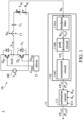
- FIG. 1 shows an exemplary embodiment of an electronic device.
- an electronic device 1 comprises a resonant circuit 10, a power detection circuit 11, a driver 12, and a current sensor 13.
- the power detection circuit 11 is used to detect current total input power of the resonant circuit 10.
- the electronic device 1 may be any device that needs to convert energy using a resonant circuit, such as a wireless signal transceiver, an induction cooker, and the like.
- the technical features of the present application will be described by taking the electronic device 1 as an induction cooker as an example.
- the resonant circuit 10 is coupled to a voltage source 100 to receive an input voltage V in .
- the resonant circuit 10 comprises an upper-arm switching element Q H , a lower-arm switching element Q L , a resonant capacitor Cr, an inductor L eq , and a resistor R eq .
- the upper-arm switching element Q H and the lower-arm switching element Q L are connected in series between the positive terminal and the negative terminal of the voltage source 100.
- the driver 12 generates switching signals G OH and G OL to control the on/off states of the upper-arm switching element Q H and the lower-arm switching element Q L , respectively.
- each of the switching signals G OH and G OL has a duty cycle, so that the controlled upper-arm switching element Q H and the lower-arm switching element Q L operate according to their corresponding duty cycles.
- the switching signals G OH and GO L Through the control of the switching signals G OH and GO L , each of the upper-arm switching element Q H and the lower-arm switching element Q L is switched between the on state and the off state, and the on time of the upper-arm switching element Q H and the on time of the lower-arm switching element Q L do not overlap.
- the inductor L eq and the resistor R eq in the resonant circuit 10 are the equivalent inductance and equivalent resistance of the pot placed on the electronic device (the induction cooker) 1, respectively.
- the resonant capacitor Cr, inductor L eq , and resistor R eq which are connected in series, form a resonant slot of the resonant circuit 10.
- the resonant circuit 10 is coupled to the common node N10 between the upper-arm switching element Q H and the lower-arm switching element Q L .
- a resonant-slot voltage v r is generated between the drain and the source of the lower-arm switching element Q L , and a resonant-slot current i r flows through the capacitor C r .
- the resonant-slot current i r flows from the common node N10 to the resonant slot. It can be discerned from the circuit structure of the resonant circuit 10 that the resonant circuit 10 is a half-bridge series resonant circuit.
- the current sensor 13 is coupled to the resonant slot of the resonant circuit 10 at the common node N10 to sense the resonant-slot current ir.
- the current sensor 13 generates a current signal Si r according to the sensed resonant-slot current ir.
- the current sensor 13 is arranged outside the power detection circuit 11. In other embodiments, the current sensor 13 may be included within the power detection circuit 11.
- the power detection circuit 11 comprises a detection circuit 110 and an estimation circuit 111.
- the detection circuit 110 receives the current signal Si r and obtains baseband power P r1 of the resonant slot according to the current signal Si r to generate the baseband power value VP r1 .
- the estimation circuit 111 receives the baseband power value VP r1 and estimates current total input power P r12 of the resonant slot according to the baseband power value VP r1 to generate an estimated power value VP r12 .
- the detailed operations of the detection circuit 110 and the estimation circuit 111 will be described below.
- the detection circuit 110 comprises a bandpass filter 110A, a peak detection circuit 110B, and a measurement circuit 110C.
- the bandpass filter 110A receives the current signal Si r from the current sensor 13 and performs a bandpass filtering operation on the current signal Si r to obtain a baseband current i r1 of the resonant slot (that is, the baseband component of the resonant-slot current i r ).
- the bandpass filter 110A generates a baseband current signal Si r1 representing the baseband current i r1 , and outputs it to the peak detection circuit 110B.
- the peak detection circuit 110B is coupled to the bandpass filter 110A and receives the baseband current signal Si r1 from the bandpass filter 110A. Since the baseband current signal Si r1 represents the baseband current i r1 , the peak detection circuit 110B can detect a peak value VP i of the baseband current i r1 according to the baseband current signal Si r1 . The peak detection circuit 110B transmits the detected peak value VP i to the measurement circuit 110C.
- the measurement circuit 110C is coupled to the peak detection circuit 110B and receives the peak value VP i .
- the parameter i r1 baseband current
- the measurement circuit 110C After the baseband power P r1 is calculated, the measurement circuit 110C generates the corresponding baseband power value VP r1 and transmits it to the estimation circuit 111.
- the value of the baseband resistance R 1 is predetermined and stored in the measurement circuit 110C in advance. In other embodiments, the value of the baseband resistance R 1 is predetermined and may be stored in a memory (not shown) of the electronic device 1 in advance. When the power detection circuit 11 operates, the value of the baseband resistance R 1 is read from the memory.
- the estimation circuit 111 is coupled to the measurement circuit 110C and receives the baseband power value VP r1 .
- the estimation circuit 111 obtains the baseband power P r1 of the resonant slot according to the baseband power value VP r1 .
- the estimation circuit 111 also receives an indication signal S11 which represents the duty cycle of the switching signal G OH .
- the estimation circuit 111 determines whether the duty cycle of the switching signal G OH is greater than a threshold value (for example, 30% or 50%) according to the indication signal S11.
- the estimation circuit 111 compensates the baseband power P r1 by a compensation parameter K to obtain the estimated current total input power P r12 , and it generates an estimated power value VP r12 according to the estimated current total input power P r12 . In cases where it is determined that the duty cycle of the switching signal G OH is greater than the threshold value, the estimation circuit 111 directly uses the baseband power value VP r1 as the estimated power value VP r12 .
- the compensation parameter K is equal to the ratio of the predetermined frequency-doubling power to the predetermined baseband power of the resonant slot at a specific duty cycle D.
- the compensation parameter K is predetermined and can be stored in the estimation circuit 111 in advance.
- the value of the compensation parameter is a predetermined parameter, which may be stored in a memory (not shown) of the electronic device 1 in advance. When the power detection circuit 11 operates, the compensation parameter K is read from the memory.
- the current total input power P r12 (the estimated power value VP r12 ) obtained in the present application is obtained with high accuracy.
- FIG. 2 shows the resonant-slot voltage v r of the resonant circuit 10 and the harmonic components of the resonant-slot voltage v r .
- the maximum value of the resonant-slot voltage v r is the input voltage V in .
- v r1 represents the baseband component of the resonant-slot voltage v r (also called the baseband voltage of the resonant slot)
- v r2 represents the frequency-doubling component of the resonant-slot voltage v r (also called the frequency-doubling voltage of the resonant slot)
- v r3 represents the frequency-tripling component of the resonant-slot voltage v r (also called the frequency-tripling component of the resonant slot).
- the peak values of the baseband voltage v r1 , the frequency-doubling voltage v r2 , and the frequency-tripling voltage v r3 are 0.515 V in , 0.303 V in , and 0.066 V in , respectively. From these values, it can be observed that the peak value of the baseband voltage v r1 is greater than the peak value of the frequency-doubling voltage v r2 and is much larger than the peak value of the frequency-tripling voltage v r3 . Therefore, the influence of the frequency-tripling voltage v r3 can be ignored for the power detection.
- the input impedance of the resonant slot increases with the increase of the operation frequency of the resonant circuit 10 it is only necessary to consider the effect of the low-order voltage harmonics (that is, the baseband harmonic and frequency-doubling harmonic) on the total input power of the resonant slot in response to the above analysis for the baseband voltage v r1 , the frequency-doubling voltage v r2 , and the frequency-tripling voltage v r3 .
- FIG. 4 shows the percentages of the baseband power P r1 , the frequency-doubling power P r2 , the frequency-tripling power P r3 , the coil loss power P coil , and the stray loss power P stray in the total power P r when the duty cycle D is 10%, 20%, 30%, 40%, and 50%, respectively.
- the duty cycle D is 10%, 20%, 30%, 40%, and 50%, respectively.
- the baseband power P r1 accounts for less than 90% of the total power P r
- the frequency-tripling power P r3 , the coil loss power P coil , and the stray loss power P stray each accounts for less than 5% of the total power P r .
- the duty cycle D is greater than 30%
- the baseband power P r1 is almost equal to the total power P r
- the frequency-doubling power P r2 , the frequency-tripling power P r3 , the coil loss power P coil , and the stray loss power P stray each also accounts for less than 5% of the total power P r .
- the estimation circuit 111 does not need to compensate the baseband power P r1 and directly uses the baseband power value VP r1 as the estimated power value VP r12 , so that the current total input power P r12 of the resonant circuit 10 can be accurately estimated.
- the baseband power P r1 accounts for less than 90% of the total power P r and the frequency-doubling power P r2 still accounts for a considerable proportion in the total power P r .
- the estimation circuit 111 compensates the baseband power P r1 using the compensation parameter K to obtain the estimated power value VP r12 .
- the estimation circuit 111 sets a threshold value and determines whether to compensate the baseband power P r1 according to whether the duty cycle D is greater than the threshold value.
- the threshold can be set to 30%.
- the compensation parameter K is the ratio of the frequency-doubling power P r2 to the baseband power P r1 .
- the parameter K v is related to the ratio of the frequency-doubling voltage v r2 to the baseband voltage v r1
- the parameter K 1 is related to the ratio of the frequency-doubling resistance and the baseband resistance.
- Equation (8) it can be known that when the duty cycle D is larger, the proportion of the double frequency power Pr2 is lower, which means that the error which is induced when the current total input power P r12 is estimated according to the baseband power P r1 is smaller.
- the parameter K 1 is determined according to the parameters K L and K R .
- FIG. 5 shows errors of parameters K L and K R and corresponding parameter K 1 under a general operation of an induction cooker. As shown in Fig. 5 , within a wide variation range of the parameters K L and K R (the areas marked with dots in FIG. 5 ), the error of parameter K 1 is less than 10%, which means that the variation range of the parameter K 1 is not large.
- the parameter K 1 can be regarded as a parameter not affected by the duty cycle D.
- the electronic device 1 can first obtain the compensation parameter K at a specific duty cycle D through a test or analysis, then obtain the parameter K v according to Equation (8), and finally estimate the parameter K 1 is according to the compensation parameter K and the parameter K v .
- the obtained compensation parameter K and the parameters K v and K 1 are stored in a memory of the electronic device 1 or stored in the estimation circuit 111 as predetermined parameters which can be used by the power detection circuit 11 during the operation.
- the electronic device 1 predetermines the compensation parameter K and the parameters K v and K 1 which all correspond to the duty cycle D of 10%.
- the estimation circuit 111 sets the threshold value as 30% as a criterion for determining whether to compensate the baseband power P r1 .
- the electronic device 1 may predetermine a plurality of compensation parameters K and a plurality of parameters K v and K 1 corresponding to a plurality of duty cycles as the predetermined parameters.
- one compensation parameter K or one set of parameters K v and K 1 among the predetermined parameters can be selected according to the indication signal S11 which represents the duty cycle D of the switching signal G OH to compensate the baseband power P r1 .
- the estimation circuit 11 determines whether to compensate the baseband power P r1 according to whether the duty cycle D is greater than a threshold value. In other embodiments, regardless of the duty cycle D of the switching signal G OH , the estimation circuit 111 compensates the baseband power P r1 according to the compensation parameter K to obtain the estimated current total input power P r12 , and generates the estimated power value VP r12 according to the estimated current total input power P r12 .
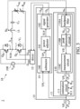
- FIG. 3 shows another exemplary embodiment of an electronic device.
- the electronic device 3 comprises a resonant circuit 10, a power detection circuit 11, a driver 12 , and a current sensor 13 as shown in FIG. 1 .
- the operations of the resonant circuit 10, the power detection circuit 11, the driver 12, and the current sensor 13 are described in the paragraphs related to the embodiment of FIG. 1 , and the description is omitted here.
- the electronic device 3 further comprises an adjustment circuit 14.
- a control circuit 15 is composed of the power detection circuit 11 and the adjustment circuit 14 for controlling the resonant circuit 10.
- the adjustment circuit 14 receives the estimated power value VP r12 from the estimation circuit 111 and generates the control signals G H and G L .
- the adjustment circuit 14 calculates a power difference between the estimated power value VP r12 and the preset power value VP r and adjusts the respective duty cycles of the control signals G H and G L according to the power difference.
- the current sensor 13 is arranged outside the control circuit 15. In other embodiments, the current sensor 13 may be included within the control circuit 15.
- the driver 12 receives the control signals G H and G L from the adjustment circuit 14 and generates the switching signals G OH and G OL according to the control signals G H and G L to control the on/off states of the upper-arm switching element Q H and the lower-arm switching element Q L , respectively. Therefore, the adjustment circuit 14 adjusts or changes the respective duty cycles of the switching signals G OH and G OL by adjusting the respective duty cycles of the control signals G H and G L .
- the duty cycle of the control signal G H is equal to the duty cycle (D) of the switching signal G OH
- the duty cycle of the control signal G L is equal to the duty cycle of the switching signal G OL .
- the adjustment circuit 14 includes a subtractor 140, a power adjuster 141, and a signal generator 142.
- the subtractor 140 receives the estimated power value VP r12 and the preset power value VP r and calculates the difference between the estimated power value VP r12 and the preset power value VP r to generate a power difference value VP d .
- the subtractor 140 transmits the power difference value VP d to the power adjuster 141.
- the power adjuster 141 receives the power difference VP d and generates an adjustment signal S14 according to at least one feature of the power difference VP d .
- the at least one feature of the power difference VP d comprises at least one of the magnitude of the power difference VP d and the polarity (positive or negative) thereof.
- the adjustment signal S14 indicates how to adjust the duty cycles of the control signals G H and G L .
- the adjustment signal S14 indicates at least one of an adjustment range and an adjustment direction (whether increasing or decreasing) for adjusting the duty cycles of the control signals G H and G L .
- the power adjuster 141 provides the adjustment signal S14 to the signal generator 142.
- the signal generator 142 receives the adjustment signal S14 and generates the control signals G H and G L .
- the signal generator 142 adjusts the duty cycles of the control signals G H and G L according to the adjustment signal S14.
- the signal generator 142 provides the control signals G H and G L to the driver 12.
- the driver 12 generates switching signals G OH and G OL according to the control signals G H and G L to control the on/off states of the upper-arm switching element Q H and the lower-arm switching element Q L , respectively.
- the control circuit 15 can estimate the current total input power P r12 of the resonant circuit 10 according to the baseband power value VP r1 to generate the estimated power value VP r12 .
- the duty cycles of the control signals G H and G L are adjusted based on the difference between the estimated power value VP r12 and the desired preset power value VP r , thereby adjusting the switching signals G OH and G OL .
- the current total input power P r12 of the resonant circuit 10 is finally close to or equal to the desired preset power value VP r .
Landscapes
- Engineering & Computer Science (AREA)
- Physics & Mathematics (AREA)
- General Physics & Mathematics (AREA)
- Power Engineering (AREA)
- Electromagnetism (AREA)
- Radar, Positioning & Navigation (AREA)
- Automation & Control Theory (AREA)
- General Engineering & Computer Science (AREA)
- Inverter Devices (AREA)
- Transmitters (AREA)
Claims (7)
- Leistungserfassungsschaltung (11) zum Erfassen der aktuellen Gesamteingangsleistung eines Resonanzkreises (10), umfassend:eine Erfassungsschaltung (110), die ein Stromsignal empfängt und eine Resonanzschlitz-Basisbandleistung gemäß dem Stromsignal erhält, um einen Basisbandleistungswert zu erzeugen, wobei das Stromsignal einen durch den Resonanzkreis erzeugten Resonanzschlitzstrom darstellt; undeine Schätzschaltung (111), die den Basisbandleistungswert empfängt und die aktuelle Gesamteingangsleistung entsprechend dem Basisbandleistungswert schätzt, um einen geschätzten Leistungswert zu erzeugen.
- Leistungserfassungsschaltung nach Anspruch 1, wobei:der Schwingkreis ein Schaltelement umfasst und das Schaltelement in Abhängigkeit von einem Tastverhältnis arbeitet, unddie Schätzschaltung die Resonanzschlitz-Basisbandleistung gemäß dem Basisbandleistungswert erhält und die Resonanzschlitz-Basisbandleistung gemäß einem Kompensationsparameter kompensiert, um den geschätzten Leistungswert zu erzeugen.
- Leistungserfassungsschaltung nach Anspruch 1 oder 2, wobei:der Schwingkreis ein Schaltelement umfasst und das Schaltelement in Abhängigkeit von einem Tastverhältnis arbeitet,wenn das Tastverhältnis größer als ein Schwellenwert ist, erhält die Schätzschaltung den Basisband-Leistungswert als geschätzten Leistungswert,wenn das Tastverhältnis nicht größer als der Schwellenwert ist, erhält die Schätzschaltung die Resonanzschlitz-Basisbandleistung gemäß dem Basisbandleistungswert und kompensiert die Resonanzschlitz-Basisbandleistung gemäß einem Kompensationsparameter, um den geschätzten Leistungswert zu erzeugen, undder Kompensationsparameter auf ein Verhältnis einer vorbestimmten Frequenzverdopplungsleistung zu einer vorbestimmten Basisbandleistung des Schwingkreises bei einem bestimmten Wert des Tastverhältnisses bezogen ist.
- Leistungserfassungsschaltung nach einem der vorhergehenden Ansprüche, wobei die Erfassungsschaltung umfasst:ein Bandpassfilter, das das Stromsignal empfängt und eine Bandpassfilterung an dem Stromsignal durchführt, um ein Basisbandstromsignal zu erzeugen, wobei das Basisbandstromsignal einen Resonanzschlitz-Basisbandstrom des Resonanzkreises darstellt;eine Spitzenwerterfassungsschaltung, die das Basisbandstromsignal empfängt und einen Spitzenwert des Resonanzschlitz-Basisbandstroms entsprechend dem Basisbandstromsignal erfasst; undeine Messschaltung, die den Spitzenwert empfängt und die Resonanzschlitz-Basisbandleistung entsprechend dem Spitzenwert und einem Basisbandwiderstand misst, um den Basisbandleistungswert zu erzeugen,wobei der Basisbandwiderstand einen Resonanzschlitz-Basisbandwiderstand des Resonanzkreises darstellt.
- Steuerschaltung zur Erzeugung eines ersten Steuersignals und eines zweiten Steuersignals zur Steuerung eines Resonanzkreises, umfassend:eine Leistungserfassungsschaltung nach einem der vorhergehenden Ansprüche; undeine Einstellschaltung, die den geschätzten Leistungswert empfängt und das erste Steuersignal erzeugt, wobei die Einstellschaltung eine Leistungsdifferenz zwischen dem geschätzten Leistungswert und einem voreingestellten Leistungswert berechnet und ein Tastverhältnis des ersten Steuersignals entsprechend der Leistungsdifferenz einstellt,wobei die Einstellschaltung ferner das zweite Steuersignal entsprechend der Leistungsdifferenz einstellt, undwobei der Schwingkreis ein oberarmiges Schaltelement und ein unterarmiges Schaltelement umfasst, die in Reihe geschaltet sind, das erste Steuersignal zur Steuerung des oberarmigen Schaltelements und das zweite Steuersignal zur Steuerung des unterarmigen Schaltelements angelegt wird.
- Steuerschaltung nach Anspruch 5, wobei:wenn das Tastverhältnis des ersten Steuersignals größer als ein Schwellenwert ist, empfängt die Schätzschaltung den Basisbandleistungswert als geschätzten Leistungswert,wenn das Tastverhältnis des ersten Steuersignals nicht größer als der Schwellenwert ist, die Abschätzungsschaltung die Resonanzschlitz-Basisbandleistung gemäß dem Basisbandleistungswert erhält und die Resonanzschlitz-Basisbandleistung gemäß einem Kompensationsparameter kompensiert, um den geschätzten Leistungswert zu erzeugen, undwobei der Kompensationsparameter mit einem Verhältnis einer vorbestimmten Frequenzverdopplungsleistung zu einer vorbestimmten Basisbandleistung des Resonanzkreises bei einem bestimmten Wert des Tastverhältnisses in Beziehung steht.
- Steuerschaltung nach Anspruch 5 oder 6, wobei die Einstellschaltung umfasst:einen Subtrahierer, der den geschätzten Leistungswert und den voreingestellten Leistungswert empfängt und die Differenz zwischen dem geschätzten Leistungswert und dem voreingestellten Leistungswert berechnet, um den Leistungsdifferenzwert zu erzeugen;eine Leistungseinstellvorrichtung, die die Leistungsdifferenz empfängt und ein Einstellsignal entsprechend mindestens einem Merkmal der Leistungsdifferenz erzeugt; undeinen Signalgenerator, der das erste Steuersignal erzeugt, wobei der Signalgenerator das Einstellsignal empfängt und das Tastverhältnis des ersten Steuersignals entsprechend dem Einstellsignal einstellt,wobei das mindestens eine Merkmal der Leistungsdifferenz mindestens eine Größe und/oder eine Polarität der Leistungsdifferenz umfasst, unddas Einstellsignal mindestens eine Einstellamplitude und eine Einstellrichtung für die Einstellung des Tastverhältnisses angibt.
Applications Claiming Priority (1)
| Application Number | Priority Date | Filing Date | Title |
|---|---|---|---|
| CN202111652210.5A CN116430111B (zh) | 2021-12-30 | 2021-12-30 | 功率检测电路以及控制电路 |
Publications (3)
| Publication Number | Publication Date |
|---|---|
| EP4206702A1 EP4206702A1 (de) | 2023-07-05 |
| EP4206702C0 EP4206702C0 (de) | 2024-05-08 |
| EP4206702B1 true EP4206702B1 (de) | 2024-05-08 |
Family
ID=83271320
Family Applications (1)
| Application Number | Title | Priority Date | Filing Date |
|---|---|---|---|
| EP22194946.4A Active EP4206702B1 (de) | 2021-12-30 | 2022-09-09 | Leistungsdetektionsschaltung und steuerschaltung |
Country Status (4)
| Country | Link |
|---|---|
| US (1) | US11789090B2 (de) |
| EP (1) | EP4206702B1 (de) |
| CN (1) | CN116430111B (de) |
| ES (1) | ES2984822T3 (de) |
Families Citing this family (1)
| Publication number | Priority date | Publication date | Assignee | Title |
|---|---|---|---|---|
| CN121917835A (zh) * | 2024-10-24 | 2026-04-24 | 台达电子工业股份有限公司 | 用于估算输入至谐振电路中谐振槽的输入功率的电子装置和方法 |
Family Cites Families (13)
| Publication number | Priority date | Publication date | Assignee | Title |
|---|---|---|---|---|
| US5334941A (en) | 1992-09-14 | 1994-08-02 | Kdc Technology Corp. | Microwave reflection resonator sensors |
| US20080316779A1 (en) * | 2007-06-19 | 2008-12-25 | Chandrasekaran Jayaraman | System and method for estimating input power for a power processing circuit |
| US8552808B2 (en) * | 2011-06-02 | 2013-10-08 | Tektronix, Inc. | Apparatus and method for oscillator resonator power control |
| JP5886025B2 (ja) | 2011-12-20 | 2016-03-16 | ルネサスエレクトロニクス株式会社 | Rf電力増幅器およびその動作方法 |
| CN102647104A (zh) * | 2012-04-13 | 2012-08-22 | 美的集团有限公司 | 一种半桥谐振电路的功率控制装置及控制方法 |
| RU2656613C2 (ru) | 2013-01-11 | 2018-06-06 | Конинклейке Филипс Н.В. | Беспроводная индуктивная передача мощности |
| US10161838B2 (en) | 2013-02-13 | 2018-12-25 | Board Of Regents, The University Of Texas System | Sensor assembly, method, and device for monitoring shear force and pressure on a structure |
| CN204068705U (zh) | 2014-09-19 | 2014-12-31 | 成都芯源系统有限公司 | 开关电源电路 |
| CN105790626B (zh) * | 2014-12-25 | 2019-02-12 | 台达电子工业股份有限公司 | 谐振型功率转换电路及控制谐振型功率转换电路的方法 |
| WO2018097820A1 (en) * | 2016-11-22 | 2018-05-31 | Power Integrations, Inc. | Switch control for resonant power converter |
| US10686382B2 (en) * | 2017-01-05 | 2020-06-16 | Stmicroelectronics S.R.L. | Symmetric time shift control for resonant converters |
| TWI694670B (zh) * | 2019-02-15 | 2020-05-21 | 群光電能科技股份有限公司 | 諧振式電源轉換裝置 |
| US11280847B1 (en) * | 2020-10-30 | 2022-03-22 | Taiwan Semiconductor Manufacturing Company Ltd. | Circuit, semiconductor device and method for parameter PSRR measurement |
-
2021
- 2021-12-30 CN CN202111652210.5A patent/CN116430111B/zh active Active
-
2022
- 2022-04-25 US US17/728,551 patent/US11789090B2/en active Active
- 2022-09-09 ES ES22194946T patent/ES2984822T3/es active Active
- 2022-09-09 EP EP22194946.4A patent/EP4206702B1/de active Active
Also Published As
| Publication number | Publication date |
|---|---|
| CN116430111B (zh) | 2025-12-05 |
| ES2984822T3 (es) | 2024-10-31 |
| EP4206702C0 (de) | 2024-05-08 |
| US11789090B2 (en) | 2023-10-17 |
| US20230213591A1 (en) | 2023-07-06 |
| CN116430111A (zh) | 2023-07-14 |
| EP4206702A1 (de) | 2023-07-05 |
Similar Documents
| Publication | Publication Date | Title |
|---|---|---|
| US12438396B2 (en) | Wireless power transfer object detection circuit and method | |
| US7084601B2 (en) | Phase current detector | |
| US5671112A (en) | Digital integrator V/Hz relay for generator and transformer over-excitation protection | |
| CN104704376B (zh) | 用于测量经过开关的电流的方法和装置 | |
| US10527666B2 (en) | Method and device for determining the fault location in the case of a fault on an electric line | |
| US11275073B2 (en) | Probing a structure of concrete by means of electromagnetic waves | |
| EP4206702B1 (de) | Leistungsdetektionsschaltung und steuerschaltung | |
| US20180048279A1 (en) | Method of automatic adjustment of a tunable matching circuit, and automatic tuning system using this method | |
| EP1777530B1 (de) | Verfahren und Vorrichtung zur Strommessung an Wechselrichterausgängen | |
| US4785236A (en) | Device for measuring voltage by scanning | |
| EP3093624B1 (de) | Selbstkalibrierender lvdt-transformator-demodulator | |
| US20180284160A1 (en) | Ultra-high bandwidth current shunt | |
| US7042135B2 (en) | Current detection circuit and current detection method | |
| US6195274B1 (en) | Method for defining instantaneous value of current of pulse-controlled inductive load | |
| US11950885B2 (en) | Biosensor device | |
| US12519347B2 (en) | Foreign object detection by frequency bandwidth comparison | |
| US6230110B1 (en) | Wheel velocity detecting apparatus | |
| TWI796918B (zh) | 功率偵測電路以及控制電路 | |
| JPH10132874A (ja) | 周波数測定装置 | |
| CN110556927A (zh) | 一种感应式无线电能传输系统的状态观测的方法及系统 | |
| US20250189566A1 (en) | Method for measuring the phase of a complex impedance | |
| CN121308377A (zh) | 无线电能传输系统的互感和负载电压识别电路及识别方法 | |
| Wang et al. | A Novel Multiple Parameters Identification Method for Wireless Power Transfer System | |
| KR100378764B1 (ko) | 대신호 파라미터 추출 장치 및 방법 | |
| JPS60148205A (ja) | 検波回路 |
Legal Events
| Date | Code | Title | Description |
|---|---|---|---|
| PUAI | Public reference made under article 153(3) epc to a published international application that has entered the european phase |
Free format text: ORIGINAL CODE: 0009012 |
|
| STAA | Information on the status of an ep patent application or granted ep patent |
Free format text: STATUS: THE APPLICATION HAS BEEN PUBLISHED |
|
| AK | Designated contracting states |
Kind code of ref document: A1 Designated state(s): AL AT BE BG CH CY CZ DE DK EE ES FI FR GB GR HR HU IE IS IT LI LT LU LV MC MK MT NL NO PL PT RO RS SE SI SK SM TR |
|
| STAA | Information on the status of an ep patent application or granted ep patent |
Free format text: STATUS: REQUEST FOR EXAMINATION WAS MADE |
|
| 17P | Request for examination filed |
Effective date: 20230811 |
|
| RBV | Designated contracting states (corrected) |
Designated state(s): AL AT BE BG CH CY CZ DE DK EE ES FI FR GB GR HR HU IE IS IT LI LT LU LV MC MK MT NL NO PL PT RO RS SE SI SK SM TR |
|
| RIC1 | Information provided on ipc code assigned before grant |
Ipc: G01R 19/00 20060101ALI20231212BHEP Ipc: H01Q 13/10 20060101ALI20231212BHEP Ipc: G01R 21/00 20060101ALI20231212BHEP Ipc: G01R 31/28 20060101AFI20231212BHEP |
|
| GRAP | Despatch of communication of intention to grant a patent |
Free format text: ORIGINAL CODE: EPIDOSNIGR1 |
|
| STAA | Information on the status of an ep patent application or granted ep patent |
Free format text: STATUS: GRANT OF PATENT IS INTENDED |
|
| INTG | Intention to grant announced |
Effective date: 20240131 |
|
| GRAS | Grant fee paid |
Free format text: ORIGINAL CODE: EPIDOSNIGR3 |
|
| GRAA | (expected) grant |
Free format text: ORIGINAL CODE: 0009210 |
|
| STAA | Information on the status of an ep patent application or granted ep patent |
Free format text: STATUS: THE PATENT HAS BEEN GRANTED |
|
| AK | Designated contracting states |
Kind code of ref document: B1 Designated state(s): AL AT BE BG CH CY CZ DE DK EE ES FI FR GB GR HR HU IE IS IT LI LT LU LV MC MK MT NL NO PL PT RO RS SE SI SK SM TR |
|
| REG | Reference to a national code |
Ref country code: GB Ref legal event code: FG4D |
|
| REG | Reference to a national code |
Ref country code: CH Ref legal event code: EP |
|
| REG | Reference to a national code |
Ref country code: DE Ref legal event code: R096 Ref document number: 602022003344 Country of ref document: DE |
|
| REG | Reference to a national code |
Ref country code: IE Ref legal event code: FG4D |
|
| U01 | Request for unitary effect filed |
Effective date: 20240528 |
|
| U07 | Unitary effect registered |
Designated state(s): AT BE BG DE DK EE FI FR IT LT LU LV MT NL PT SE SI Effective date: 20240606 |
|
| U20 | Renewal fee for the european patent with unitary effect paid |
Year of fee payment: 3 Effective date: 20240822 |
|
| PG25 | Lapsed in a contracting state [announced via postgrant information from national office to epo] |
Ref country code: IS Free format text: LAPSE BECAUSE OF FAILURE TO SUBMIT A TRANSLATION OF THE DESCRIPTION OR TO PAY THE FEE WITHIN THE PRESCRIBED TIME-LIMIT Effective date: 20240908 |
|
| PG25 | Lapsed in a contracting state [announced via postgrant information from national office to epo] |
Ref country code: HR Free format text: LAPSE BECAUSE OF FAILURE TO SUBMIT A TRANSLATION OF THE DESCRIPTION OR TO PAY THE FEE WITHIN THE PRESCRIBED TIME-LIMIT Effective date: 20240508 |
|
| PG25 | Lapsed in a contracting state [announced via postgrant information from national office to epo] |
Ref country code: GR Free format text: LAPSE BECAUSE OF FAILURE TO SUBMIT A TRANSLATION OF THE DESCRIPTION OR TO PAY THE FEE WITHIN THE PRESCRIBED TIME-LIMIT Effective date: 20240809 |
|
| PG25 | Lapsed in a contracting state [announced via postgrant information from national office to epo] |
Ref country code: PL Free format text: LAPSE BECAUSE OF FAILURE TO SUBMIT A TRANSLATION OF THE DESCRIPTION OR TO PAY THE FEE WITHIN THE PRESCRIBED TIME-LIMIT Effective date: 20240508 |
|
| PG25 | Lapsed in a contracting state [announced via postgrant information from national office to epo] |
Ref country code: PL Free format text: LAPSE BECAUSE OF FAILURE TO SUBMIT A TRANSLATION OF THE DESCRIPTION OR TO PAY THE FEE WITHIN THE PRESCRIBED TIME-LIMIT Effective date: 20240508 Ref country code: NO Free format text: LAPSE BECAUSE OF FAILURE TO SUBMIT A TRANSLATION OF THE DESCRIPTION OR TO PAY THE FEE WITHIN THE PRESCRIBED TIME-LIMIT Effective date: 20240808 Ref country code: IS Free format text: LAPSE BECAUSE OF FAILURE TO SUBMIT A TRANSLATION OF THE DESCRIPTION OR TO PAY THE FEE WITHIN THE PRESCRIBED TIME-LIMIT Effective date: 20240908 Ref country code: HR Free format text: LAPSE BECAUSE OF FAILURE TO SUBMIT A TRANSLATION OF THE DESCRIPTION OR TO PAY THE FEE WITHIN THE PRESCRIBED TIME-LIMIT Effective date: 20240508 Ref country code: GR Free format text: LAPSE BECAUSE OF FAILURE TO SUBMIT A TRANSLATION OF THE DESCRIPTION OR TO PAY THE FEE WITHIN THE PRESCRIBED TIME-LIMIT Effective date: 20240809 Ref country code: RS Free format text: LAPSE BECAUSE OF FAILURE TO SUBMIT A TRANSLATION OF THE DESCRIPTION OR TO PAY THE FEE WITHIN THE PRESCRIBED TIME-LIMIT Effective date: 20240808 |
|
| REG | Reference to a national code |
Ref country code: ES Ref legal event code: FG2A Ref document number: 2984822 Country of ref document: ES Kind code of ref document: T3 Effective date: 20241031 |
|
| PG25 | Lapsed in a contracting state [announced via postgrant information from national office to epo] |
Ref country code: CZ Free format text: LAPSE BECAUSE OF FAILURE TO SUBMIT A TRANSLATION OF THE DESCRIPTION OR TO PAY THE FEE WITHIN THE PRESCRIBED TIME-LIMIT Effective date: 20240508 |
|
| PG25 | Lapsed in a contracting state [announced via postgrant information from national office to epo] |
Ref country code: SK Free format text: LAPSE BECAUSE OF FAILURE TO SUBMIT A TRANSLATION OF THE DESCRIPTION OR TO PAY THE FEE WITHIN THE PRESCRIBED TIME-LIMIT Effective date: 20240508 Ref country code: RO Free format text: LAPSE BECAUSE OF FAILURE TO SUBMIT A TRANSLATION OF THE DESCRIPTION OR TO PAY THE FEE WITHIN THE PRESCRIBED TIME-LIMIT Effective date: 20240508 |
|
| PG25 | Lapsed in a contracting state [announced via postgrant information from national office to epo] |
Ref country code: SM Free format text: LAPSE BECAUSE OF FAILURE TO SUBMIT A TRANSLATION OF THE DESCRIPTION OR TO PAY THE FEE WITHIN THE PRESCRIBED TIME-LIMIT Effective date: 20240508 |
|
| PG25 | Lapsed in a contracting state [announced via postgrant information from national office to epo] |
Ref country code: SM Free format text: LAPSE BECAUSE OF FAILURE TO SUBMIT A TRANSLATION OF THE DESCRIPTION OR TO PAY THE FEE WITHIN THE PRESCRIBED TIME-LIMIT Effective date: 20240508 Ref country code: SK Free format text: LAPSE BECAUSE OF FAILURE TO SUBMIT A TRANSLATION OF THE DESCRIPTION OR TO PAY THE FEE WITHIN THE PRESCRIBED TIME-LIMIT Effective date: 20240508 Ref country code: RO Free format text: LAPSE BECAUSE OF FAILURE TO SUBMIT A TRANSLATION OF THE DESCRIPTION OR TO PAY THE FEE WITHIN THE PRESCRIBED TIME-LIMIT Effective date: 20240508 Ref country code: CZ Free format text: LAPSE BECAUSE OF FAILURE TO SUBMIT A TRANSLATION OF THE DESCRIPTION OR TO PAY THE FEE WITHIN THE PRESCRIBED TIME-LIMIT Effective date: 20240508 |
|
| REG | Reference to a national code |
Ref country code: DE Ref legal event code: R097 Ref document number: 602022003344 Country of ref document: DE |
|
| PLBE | No opposition filed within time limit |
Free format text: ORIGINAL CODE: 0009261 |
|
| STAA | Information on the status of an ep patent application or granted ep patent |
Free format text: STATUS: NO OPPOSITION FILED WITHIN TIME LIMIT |
|
| 26N | No opposition filed |
Effective date: 20250211 |
|
| PG25 | Lapsed in a contracting state [announced via postgrant information from national office to epo] |
Ref country code: MC Free format text: LAPSE BECAUSE OF FAILURE TO SUBMIT A TRANSLATION OF THE DESCRIPTION OR TO PAY THE FEE WITHIN THE PRESCRIBED TIME-LIMIT Effective date: 20240508 |
|
| PG25 | Lapsed in a contracting state [announced via postgrant information from national office to epo] |
Ref country code: IE Free format text: LAPSE BECAUSE OF NON-PAYMENT OF DUE FEES Effective date: 20240909 |
|
| U20 | Renewal fee for the european patent with unitary effect paid |
Year of fee payment: 4 Effective date: 20250807 |
|
| PGFP | Annual fee paid to national office [announced via postgrant information from national office to epo] |
Ref country code: TR Payment date: 20250905 Year of fee payment: 4 |
|
| PG25 | Lapsed in a contracting state [announced via postgrant information from national office to epo] |
Ref country code: CY Free format text: LAPSE BECAUSE OF FAILURE TO SUBMIT A TRANSLATION OF THE DESCRIPTION OR TO PAY THE FEE WITHIN THE PRESCRIBED TIME-LIMIT; INVALID AB INITIO Effective date: 20220909 |
|
| PGFP | Annual fee paid to national office [announced via postgrant information from national office to epo] |
Ref country code: ES Payment date: 20251014 Year of fee payment: 4 |
|
| PG25 | Lapsed in a contracting state [announced via postgrant information from national office to epo] |
Ref country code: HU Free format text: LAPSE BECAUSE OF FAILURE TO SUBMIT A TRANSLATION OF THE DESCRIPTION OR TO PAY THE FEE WITHIN THE PRESCRIBED TIME-LIMIT; INVALID AB INITIO Effective date: 20220909 |
|
| REG | Reference to a national code |
Ref country code: CH Ref legal event code: H13 Free format text: ST27 STATUS EVENT CODE: U-0-0-H10-H13 (AS PROVIDED BY THE NATIONAL OFFICE) Effective date: 20260425 |