EP4205175B1 - Dreidimensionale speichervorrichtung und verfahren zur herstellung davon - Google Patents
Dreidimensionale speichervorrichtung und verfahren zur herstellung davon Download PDFInfo
- Publication number
- EP4205175B1 EP4205175B1 EP22817512.1A EP22817512A EP4205175B1 EP 4205175 B1 EP4205175 B1 EP 4205175B1 EP 22817512 A EP22817512 A EP 22817512A EP 4205175 B1 EP4205175 B1 EP 4205175B1
- Authority
- EP
- European Patent Office
- Prior art keywords
- memory
- isolation structure
- region
- dummy
- forming
- Prior art date
- Legal status (The legal status is an assumption and is not a legal conclusion. Google has not performed a legal analysis and makes no representation as to the accuracy of the status listed.)
- Active
Links
Images









Classifications
-
- H—ELECTRICITY
- H10—SEMICONDUCTOR DEVICES; ELECTRIC SOLID-STATE DEVICES NOT OTHERWISE PROVIDED FOR
- H10B—ELECTRONIC MEMORY DEVICES
- H10B43/00—EEPROM devices comprising charge-trapping gate insulators
- H10B43/20—EEPROM devices comprising charge-trapping gate insulators characterised by three-dimensional [3D] arrangements, e.g. with cells on different height levels
- H10B43/23—EEPROM devices comprising charge-trapping gate insulators characterised by three-dimensional [3D] arrangements, e.g. with cells on different height levels with source and drain on different levels, e.g. with sloping channels
- H10B43/27—EEPROM devices comprising charge-trapping gate insulators characterised by three-dimensional [3D] arrangements, e.g. with cells on different height levels with source and drain on different levels, e.g. with sloping channels the channels comprising vertical portions, e.g. U-shaped channels
-
- H—ELECTRICITY
- H10—SEMICONDUCTOR DEVICES; ELECTRIC SOLID-STATE DEVICES NOT OTHERWISE PROVIDED FOR
- H10B—ELECTRONIC MEMORY DEVICES
- H10B41/00—Electrically erasable-and-programmable ROM [EEPROM] devices comprising floating gates
- H10B41/10—Electrically erasable-and-programmable ROM [EEPROM] devices comprising floating gates characterised by the top-view layout
-
- H—ELECTRICITY
- H10—SEMICONDUCTOR DEVICES; ELECTRIC SOLID-STATE DEVICES NOT OTHERWISE PROVIDED FOR
- H10B—ELECTRONIC MEMORY DEVICES
- H10B41/00—Electrically erasable-and-programmable ROM [EEPROM] devices comprising floating gates
- H10B41/20—Electrically erasable-and-programmable ROM [EEPROM] devices comprising floating gates characterised by three-dimensional [3D] arrangements, e.g. with cells on different height levels
- H10B41/23—Electrically erasable-and-programmable ROM [EEPROM] devices comprising floating gates characterised by three-dimensional [3D] arrangements, e.g. with cells on different height levels with source and drain on different levels, e.g. with sloping channels
- H10B41/27—Electrically erasable-and-programmable ROM [EEPROM] devices comprising floating gates characterised by three-dimensional [3D] arrangements, e.g. with cells on different height levels with source and drain on different levels, e.g. with sloping channels the channels comprising vertical portions, e.g. U-shaped channels
-
- H—ELECTRICITY
- H10—SEMICONDUCTOR DEVICES; ELECTRIC SOLID-STATE DEVICES NOT OTHERWISE PROVIDED FOR
- H10B—ELECTRONIC MEMORY DEVICES
- H10B41/00—Electrically erasable-and-programmable ROM [EEPROM] devices comprising floating gates
- H10B41/40—Electrically erasable-and-programmable ROM [EEPROM] devices comprising floating gates characterised by the peripheral circuit region
-
- H—ELECTRICITY
- H10—SEMICONDUCTOR DEVICES; ELECTRIC SOLID-STATE DEVICES NOT OTHERWISE PROVIDED FOR
- H10B—ELECTRONIC MEMORY DEVICES
- H10B41/00—Electrically erasable-and-programmable ROM [EEPROM] devices comprising floating gates
- H10B41/50—Electrically erasable-and-programmable ROM [EEPROM] devices comprising floating gates characterised by the boundary region between the core region and the peripheral circuit region
-
- H—ELECTRICITY
- H10—SEMICONDUCTOR DEVICES; ELECTRIC SOLID-STATE DEVICES NOT OTHERWISE PROVIDED FOR
- H10B—ELECTRONIC MEMORY DEVICES
- H10B43/00—EEPROM devices comprising charge-trapping gate insulators
- H10B43/10—EEPROM devices comprising charge-trapping gate insulators characterised by the top-view layout
-
- H—ELECTRICITY
- H10—SEMICONDUCTOR DEVICES; ELECTRIC SOLID-STATE DEVICES NOT OTHERWISE PROVIDED FOR
- H10B—ELECTRONIC MEMORY DEVICES
- H10B43/00—EEPROM devices comprising charge-trapping gate insulators
- H10B43/40—EEPROM devices comprising charge-trapping gate insulators characterised by the peripheral circuit region
-
- H—ELECTRICITY
- H10—SEMICONDUCTOR DEVICES; ELECTRIC SOLID-STATE DEVICES NOT OTHERWISE PROVIDED FOR
- H10B—ELECTRONIC MEMORY DEVICES
- H10B43/00—EEPROM devices comprising charge-trapping gate insulators
- H10B43/50—EEPROM devices comprising charge-trapping gate insulators characterised by the boundary region between the core and peripheral circuit regions
Definitions
- the present disclosure relates to memory devices and methods for forming memory devices.
- Planar semiconductor devices such as memory cells
- Planar semiconductor devices are scaled to smaller sizes by improving process technology, circuit design, programming algorithm, and fabrication process.
- process technology circuit design, programming algorithm, and fabrication process.
- feature sizes of the semiconductor devices approach a lower limit
- planar process and fabrication techniques become challenging and costly.
- a three-dimensional (3D) semiconductor device architecture can address the density limitation in some planar semiconductor devices, for example, Flash memory devices.
- US 2020/152653 A1 describes a through array contact structure of three-dimensional memory device with dummy channel regions between memory blocks.
- WO 2021/155611 A1 describes a blockto-block isolation and deep contact using pillars in memory array.
- CN 111 883 534 A describes a semiconductor device with a plurality of transistors.
- a 3D memory device according to claim 1 is disclosed.
- the dummy structure includes a plurality of second conductive layers and a plurality of second dielectric layers alternately stacked along the second direction.
- the plurality of first conductive layers and the plurality of second conductive layers are same layers, and the plurality of first dielectric layers and the plurality of second dielectric layers are same layer.
- the dummy structure further includes a dummy channel structure extending through the plurality of second conductive layers and the plurality of second dielectric layers along the second direction, wherein the dummy channel structure includes a semiconductor channel and a memory film formed over the semiconductor channel.
- the dummy structure further includes a contact structure extending through the plurality of second conductive layers and the plurality of second dielectric layers along the second direction.
- the contact structure further includes a contact extending through the plurality of second conductive layers and the plurality of second dielectric layers along the second direction, and a third dielectric layer extending along the second direction surrounding the contact.
- a third conductive layer is disposed in the semiconductor layer extending along the second direction under the contact, wherein the third conductive layer is in electric contact with the contact and is surrounded by a third dielectric layer.
- the trench isolation structure electrically isolates the semiconductor layer under each memory stack.
- Trench isolation structure is disposed under the first and the second isolation structures and aligns to the first and the second isolation structures.
- the trench isolation structure is disposed under the dummy structure.
- the first isolation structure further includes a gate line slit extending along the second direction and the third direction.
- the first isolation structure electrically isolates the plurality of first conductive layers and the plurality of second conductive layers.
- the plurality of channel structures are formed in the first memory region, the second memory region, and the dummy region along the second direction.
- the plurality of channel structures are formed in the first memory region and the second memory region.
- a contact structure is formed in the dummy region along the second direction.
- a first gate line slit structure is formed in the first slit and a second gate line slit structure is formed in the second slit.
- a second dielectric layer is formed in the first slit and a third dielectric layer is formed in the second slit.
- an opening is formed in the semiconductor layer under the first isolation structure and the second isolation structure from a bottom side of the stack structure opposite to the upper side.
- a fourth dielectric layer is formed in the opening.
- the first isolation structure electrically isolates the plurality of conductive layers between the first memory region and the dummy region
- the second isolation structure electrically isolates the plurality of conductive layers between the second memory region and the dummy region
- the third isolation structure electrically isolates the semiconductor layer under the first memory region and the dummy region
- the fourth isolation structure electrically isolates the semiconductor layer under the second memory region and the dummy region
- terminology may be understood at least in part from usage in context.
- the term “one or more” as used herein, depending at least in part upon context may be used to describe any feature, structure, or characteristic in a singular sense or may be used to describe combinations of features, structures or characteristics in a plural sense.
- terms, such as “a,” “an,” or “the,” again, may be understood to convey a singular usage or to convey a plural usage, depending at least in part upon context.
- the term “based on” may be understood as not necessarily intended to convey an exclusive set of factors and may, instead, allow for existence of additional factors not necessarily expressly described, again, depending at least in part on context.
- spatially relative terms such as “beneath,” “below,” “lower,” “above,” “upper,” and the like, may be used herein for ease of description to describe one element or feature's relationship to another element(s) or feature(s) as illustrated in the figures.
- the spatially relative terms are intended to encompass different orientations of the device in use or operation in addition to the orientation depicted in the figures.
- the apparatus may be otherwise oriented (rotated 90 degrees or at other orientations), and the spatially relative descriptors used herein may likewise be interpreted accordingly.
- a layer refers to a material portion including a region with a thickness.
- a layer can extend over the entirety of an underlying or overlying structure or may have an extent less than the extent of an underlying or overlying structure. Further, a layer can be a region of a homogeneous or inhomogeneous continuous structure that has a thickness less than the thickness of the continuous structure. For example, a layer can be located between any pair of horizontal planes between, or at, a top surface and a bottom surface of the continuous structure. A layer can extend horizontally, vertically, and/or along a tapered surface.
- a substrate can be a layer, can include one or more layers therein, and/or can have one or more layer thereupon, thereabove, and/or therebelow.
- a layer can include multiple layers.
- an interconnect layer can include one or more conductor and contact layers (in which interconnect lines and/or via contacts are formed) and one or more dielectric layers.
- the term "substrate” refers to a material onto which subsequent material layers are added.
- the substrate itself can be patterned. Materials added on top of the substrate can be patterned or can remain unpatterned.
- the substrate can include a wide array of semiconductor materials, such as silicon, germanium, gallium arsenide, indium phosphide, etc.
- the substrate can be made from an electrically non-conductive material, such as a glass, a plastic, or a sapphire wafer.
- 3D memory device refers to a semiconductor device with vertically oriented strings of memory cell transistors (referred to herein as “memory strings,” such as NAND memory strings) on a laterally-oriented substrate so that the memory strings extend in the vertical direction with respect to the substrate.
- memory strings such as NAND memory strings
- vertical/vertically means nominally perpendicular to the lateral surface of a substrate.
- a 3D semiconductor device can be formed by stacking semiconductor wafers or dies and interconnecting them vertically so that the resulting structure acts as a single device to achieve performance improvements at reduced power and a smaller footprint than conventional planar processes.
- the charge lateral migration issue becomes a major issue of the 3D semiconductor device.
- a stack of devices includes memory array devices and peripheral devices. As the shrinkage of the device size and thickness, the distance between the word lines becomes smaller and smaller. Hence, the charge lateral migration issue in the channel structure is one of the bottlenecks of the 3D NAND memory devices.
- FIG. 1 illustrates a plan view of an exemplary 3D memory device 100, according to some aspects of the present disclosure.
- 3D memory device 100 includes a plurality of planes and a dummy region is formed between two adjacent planes along the y-direction.
- 3D memory device 100 is divided into a first memory region 102, a second memory region 104, and a dummy region 106.
- a first isolation structure 108 is disposed between first memory region 102 and dummy region 106
- a second isolation structure 109 is disposed between second memory region 104 and dummy region 106.
- First isolation structure 108 and second isolation structure 109 may extend along the x-direction and the z-direction.
- a plurality of channel structures 110 may be formed in first memory region 102 and second memory region 104. Channel structures 110 may extend along the z-direction perpendicular to the x-direction and the y-direction.
- a plurality of dummy channel structures 112 may be formed in dummy region 106. Similarly, dummy channel structures 112 may extend along the z-direction perpendicular to the x-direction and the y-direction.
- FIG. 2 illustrates a cross-section of 3D memory device 100, according to some aspects of the present disclosure.
- First memory region 102, dummy region 106, and second memory region 104 are arranged along the y-direction on a substrate 118.
- substrate 118 is a semiconductor layer.
- substrate 118 may include silicon (e.g., single crystalline silicon), silicon germanium (SiGe), gallium arsenide (GaAs), germanium (Ge), silicon on insulator (SOI), germanium on insulator (GOI), or any other suitable materials.
- substrate 118 may be a thinned substrate (e.g., a semiconductor layer), which was thinned by grinding, wet/dry etching, chemical mechanical polishing (CMP), or any combination thereof.
- CMP chemical mechanical polishing
- First isolation structure 108 and second isolation structure 109 are formed between first memory region 102 and dummy region 106, and between second memory region 104 and dummy region 106.
- Each of first memory region 102 and second memory region 104 may include a plurality of first conductive layers 114 (such as the word lines) and a plurality of first dielectric layers 116 alternately stacked along the z-direction.
- dummy region 106 may include a plurality of conductive layers and a plurality of dielectric layers alternately stacked along the z-direction.
- the plurality of conductive layers and the plurality of dielectric layers formed in dummy region 106 may be formed in the same processes with first conductive layers 114 and first dielectric layers 116 in first memory region 102 and second memory region 104. In other words, even though the conductive layers and the dielectric layers are divided in first memory region 102, second memory region 104, and dummy region 106, the conductive layers and the dielectric layers may be formed together during the manufacturing process.
- first conductive layers 114 may form the word lines and may include conductive materials including, but not limited to, tungsten (W), cobalt (Co), copper (Cu), aluminum (Al), polysilicon, doped silicon, silicides, or any combination thereof.
- first dielectric layers 116 may include dielectric materials including, but not limited to, silicon oxide, silicon nitride, silicon oxynitride, or any combination thereof.
- channel structures 110 may include a semiconductor channel and a memory film formed over the semiconductor channel.
- the memory film may be a multilayer structure and is an element to achieve the storage function in 3D memory device 100.
- the memory film may include a composite layer of silicon oxide/silicon oxynitride/silicon oxide (ONO).
- the ONO structure may be formed on the surface of the semiconductor channel, and the ONO structure (the memory film) is also located between the semiconductor channel and first conductive layers 114, such as word lines.
- the semiconductor channel may include silicon, such as amorphous silicon, polysilicon, or single crystalline silicon.
- dummy channel structures 112 may have the same structure with channel structures 110, as shown in FIG. 2 . In some implementations, dummy channel structures 112 and channel structures 110 may have different structures, as shown in FIG. 5 or FIG. 9 .
- first isolation structure 108 may extend along the z-direction and the x-direction between first memory region 102 and dummy region 106
- second isolation structure 109 may extend along the z-direction and the x-direction between second memory region 104 and dummy region 106
- first isolation structure 108 and second isolation structure 109 may include a gate line slit structure.
- the gate line slit structure may extend along the z-direction through the memory stacks and may also extend along the x-direction to separate the memory stacks into multiple blocks.
- the gate line slit structure may include a slit contact, formed by filling the slit opening with conductive materials including but not limited to W, Co, Cu, Al, polysilicon, silicides, or any combination thereof.
- the gate line slit structure may further include a composite spacer disposed laterally between the slit contact and first conductive layers 114 and first dielectric layers 116 to electrically insulate the gate line slit structure from surrounding first conductive layers 114 (the gate conductors in the memory stacks).
- the gate line slit structure including first isolation structure 108 and second isolation structure 109, electrically separates the memory stacks in first memory region 102, dummy region 106, and second memory region 104.
- first isolation structure 108 and second isolation structure 109 may include a barrier structure formed by dielectric materials.
- the barrier structure may extend vertically along the z-direction through the memory stacks and may also extend laterally along the x-direction to separate the memory stacks into multiple blocks.
- the barrier structure may include one or multiple dielectric layers to electrically separates the memory stacks in first memory region 102, dummy region 106, and second memory region 104.
- 3D memory device 100 may further include a third isolation structure 120.
- Third isolation structure 120 may be formed in substrate 118 extending along the z-direction.
- Third isolation structure 120 is a trench isolation structure formed in substrate 118.
- third isolation structure 120 may be formed by dielectric materials.
- Third isolation structure 120 may electrically isolate substrate 118 in first memory region 102, dummy region 106, and second memory region 104.
- substrate 118 is formed by semiconductor materials, e.g., silicon, the well regions of the semiconductor substrate under different memory stacks need to be electrically isolated.
- third isolation structure 120 may align to first isolation structure 108 and second isolation structure 109 in the z-direction.
- third isolation structure 120 may not align to first isolation structure 108 and second isolation structure 109 in the z-direction, and the well regions of the semiconductor substrate under different memory stacks are isolated by third isolation structure 120.
- second isolation structure 120 By forming second isolation structure 120, the well regions of substrate 118 under different memory stacks can be electrically isolated without a complicated structure.
- FIG. 3 illustrates a cross-section of another exemplary 3D memory device 200, according to some aspects of the present disclosure.
- the structure of 3D memory device 200 may be similar to the structure of 3D memory device 100.
- 3D memory device 200 may include a fourth isolation structure 220, which does not align to first isolation structure 108 or second isolation structure 109.
- fourth isolation structure 220 may be formed in substrate 118 extending along the z-direction.
- fourth isolation structure 220 may be formed by dielectric materials.
- Fourth isolation structure 220 may electrically isolate substrate 118 in first memory region 102, and second memory region 104.
- fourth isolation structure 220 may be formed in dummy region 106.
- fourth isolation structure 220 may align to dummy channel structures 112.
- fourth isolation structure 220 may not align to dummy channel structures 112.
- FIG. 4 illustrates a cross-section of still another exemplary 3D memory device 300, according to some aspects of the present disclosure.
- the structure of 3D memory device 300 may be similar to the structure of 3D memory device 100. However, 3D memory device 300 does not include the dummy region.
- first memory region 102 and second memory region 104 are arranged along the y-direction on a substrate 118.
- substrate 118 may include silicon (e.g., single crystalline silicon), SiGe, GaAs, Ge, SOI, GOI, or any other suitable materials.
- substrate 118 may be a thinned substrate (e.g., a semiconductor layer), which was thinned by grinding, wet/dry etching, CMP, or any combination thereof.
- First isolation structure 108 is formed between first memory region 102 and second memory region 104.
- first memory region 102 and second memory region 104 may include first conductive layers 114 (such as the word lines) and first dielectric layers 116 alternately stacked along the z-direction.
- channel structures 110 may include a semiconductor channel, and a memory film formed over the semiconductor channel.
- first isolation structure 108 may extend vertically along the z-direction and the x-direction between first memory region 102 and second memory region.
- first isolation structure 108 may include a gate line slit structure.
- the gate line slit structure may extend vertically along the z-direction through the memory stacks and may also extend laterally along the x-direction to separate the memory stacks into multiple blocks.
- the gate line slit structure may include a slit contact, formed by filling the slit opening with conductive materials including but not limited to, W, Co, Cu, Al, polysilicon, silicides, or any combination thereof.
- the gate line slit structure may further include a composite spacer disposed laterally between the slit contact and first conductive layers 114 and first dielectric layers 116 to electrically insulate the gate line slit structure from surrounding first conductive layers 114 (the gate conductors in the memory stacks). As a result, the gate line slit structure electrically separates the memory stacks in first memory region 102 and second memory region 104.
- first isolation structure 108 may include a barrier structure formed by dielectric materials.
- the barrier structure may extend vertically along the z-direction through the memory stacks and may also extend laterally along the x-direction to separate the memory stacks into multiple blocks.
- the barrier structure may include one or multiple dielectric layers to electrically separates the memory stacks in first memory region 102 and second memory region 104.
- third isolation structure 120 may be formed in substrate 118 extending along the z-direction aligning to first isolation structure 108. In some implementations, third isolation structure 120 may be formed in substrate 118 extending along the z-direction not aligning to first isolation structure 108. In some implementations, third isolation structure 120 may be formed by dielectric material that may electrically isolate the well regions of the semiconductor substrate under different memory stacks. In some implementations, third isolation structure 120 may be formed by a conductive structure surrounded by dielectric layer and may electrically isolate the well regions of the semiconductor substrate under different memory stacks. By forming second isolation structure 120, the well regions of substrate 118 under different memory stacks can be electrically isolated without a complicated structure.
- FIG. 5 illustrates a cross-section of yet another exemplary 3D memory device 400, according to some aspects of the present disclosure.
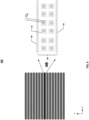
- FIG. 6 illustrates a plan view of 3D memory device 400, according to some aspects of the present disclosure.
- the cross-section and the plan view of 3D memory device 400 in FIG. 5 and FIG. 6 will be discussed together.
- 3D memory device 400 is divided into first memory region 102, second memory region 104, and a dummy region 406.
- First isolation structure 108 is disposed between first memory region 102 and dummy region 406, and second isolation structure 109 is disposed between second memory region 104 and dummy region 406.
- First isolation structure 108 and second isolation structure 109 may extend along the z-direction and the x-direction.
- Channel structures 110 may be formed in first memory region 102 and second memory region 104. Channel structures 110 may extend along the z-direction perpendicular to the x-direction and the y-direction.
- First memory region 102, dummy region 406, and second memory region 104 are arranged along the y-direction on substrate 118.
- substrate 118 may include silicon (e.g., single crystalline silicon), SiGe, GaAs, Ge, SOI, GOI, or any other suitable materials.
- substrate 118 may be a thinned substrate (e.g., a semiconductor layer), which was thinned by grinding, wet/dry etching, CMP, or any combination thereof.
- First isolation structure 108 is formed between first memory region 102 and dummy region 406, and second isolation structure 109 is formed between second memory region 104 and dummy region 406.
- Each of first memory region 102 and second memory region 104 may include first conductive layers 114 (such as the word lines) and dielectric layers 116 alternately stacked along the z-direction.
- dummy region 406 may include a plurality of conductive layers and a plurality of dielectric layers alternately stacked along the z-direction.
- the plurality of conductive layers and the plurality of dielectric layers formed in dummy region 406 may be formed in the same processes with first conductive layers 114 and first dielectric layers 116 in first memory region 102 and second memory region 104.
- first conductive layers 114, first dielectric layers 116, channel structures 110, first isolation structure 108, and second isolation structure 120 of 3D memory device 400 may be similar to those of 3D memory device 100.
- each contact structure 412 may include a first conductive contact 413 extending along the z-direction through conductive layers 114 and dielectric layers 116.
- first conductive contact 413 may include W, Co, Cu, Al, polysilicon, silicides, or other suitable materials.
- Contact structures 412 may further include a spacer 411 disposed laterally between first conductive contact 413 and first conductive layers 114 and first dielectric layers 116 to electrically insulate first conductive contact 413 from surrounding first conductive layers 114 (the gate conductors in the memory stacks).
- 3D memory device 400 further includes a second conductive contact 420 formed under contact structures 412.
- first conductive contact 413 is in direct contact with second conductive contact 420.
- second conductive contact 420 may include W, Co, Cu, Al, polysilicon, silicides, or other suitable materials.
- the source terminals of 3D memory device 400 may be connected to the peripheral device through the conductive paths formed by contact structures 412 and second conductive contact 420, and therefore the peripheral device may control the operations of 3D memory device 400.
- the conductive paths formed by contact structures 412 and second conductive contact 420 may be used to connected other devices disposed above, below, or aside 3D memory device 400.
- the peripheral device may include one or more peripheral circuits.
- the peripheral circuits may be electrically connected to 3D memory device 400 through the conductive wires, such as the redistribution layers.
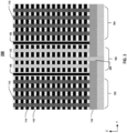
- FIG. 7 illustrates a cross-section along line A in FIG. 8 of yet another exemplary 3D memory device 500, according to some aspects of the present disclosure.
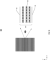
- FIG. 8 illustrates a plan view of 3D memory device 500, according to some aspects of the present disclosure.
- the cross-section and the plan view of 3D memory device 500 in FIG. 7 and FIG. 8 will be discussed together.
- 3D memory device 500 is divided into first memory region 102, second memory region 104, and a dummy region 506.
- First isolation structure 108 is disposed between first memory region 102 and dummy region 506, and second isolation structure 109 is disposed between second memory region 104 and dummy region 506.
- one or more than one fifth isolation structure 550 is also disposed in dummy region 506, as shown in FIG, 7 .
- First isolation structure 108, second isolation structure 109, and fifth isolation structure 550 may extend along the x-direction and the z-direction.
- Channel structures 110 may be formed in first memory region 102 and second memory region 104.
- Channel structures 110 may extend along the z-direction perpendicular to the x-direction and the y-direction.
- Dummy channel structures 112 may be formed in dummy region 506.
- dummy channel structures 112 may extend along the z-direction perpendicular to the x-direction and the y-direction.
- First memory region 102, dummy region 506, and second memory region 104 are arranged along the y-direction on substrate 118.
- Each of first memory region 102, dummy region 506, and second memory region 104 may include first conductive layers 114 (such as the word lines) and dielectric layers 116 alternately stacked along the z-direction.
- first conductive layers 114, first dielectric layers 116, channel structures 110, first isolation structure 108, second isolation structure 109, and third isolation structure 120 of 3D memory device 500 may be similar to those of 3D memory device 100.
- 3D memory device 500 further includes a sixth isolation structure 558 disposed under dummy channel structures 112.
- sixth isolation structure 558 may be formed in substrate 118 extending along the z-direction.
- the structure and material of sixth isolation structure 558 may be similar to those of third isolation structure 120.
- 3D memory device 500 further includes a conductive contact 556 disposed under fifth isolation structure 550 in dummy block region 506.
- conductive contact 556 is surrounded by a dielectric layer.
- fifth isolation structure 550 may include a gate line slit structure.
- the gate line slit structure may extend vertically along the z-direction through the memory stacks, as shown in FIG. 7 , and may also extend laterally along the x-direction, as shown in FIG. 8 .
- the gate line slit structure may include a slit contact 552, formed by filling the slit opening with conductive materials including but not limited to W, Co, Cu, Al, polysilicon, silicides, or any combination thereof.
- the gate line slit structure may further include a composite spacer 554 disposed laterally between the slit contact and first conductive layers 114 and first dielectric layers 116 to electrically insulate the gate line slit structure from surrounding first conductive layers 114 (the gate conductors in the memory stacks). As a result, the gate line slit structure electrically separates the memory stacks in first memory region 102, dummy region 506, and second memory region 104.
- conductive contact 556 in dummy block region 506 By forming conductive contact 556 in dummy block region 506 in direct contact with fifth isolation structure 550, slit contact 552 is in direct contact with conductive contact 556. Hence, in dummy block region 506, fifth isolation structure 550 and conductive contact 556 may provide conductive paths through the memory stacks and the silicon substrate.
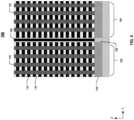
- FIG. 9 illustrates a cross-section of yet another exemplary 3D memory device 600, according to some aspects of the present disclosure.
- FIG. 10 illustrates a plan view of 3D memory device 600, according to some aspects of the present disclosure.
- the cross-section and the plan view of 3D memory device 600 in FIG. 9 and FIG. 10 will be discussed together.
- 3D memory device 600 is divided into first memory region 102, second memory region 104, and a dummy region 606.
- First isolation structure 108 is disposed between first memory region 102 and dummy region 606, and second isolation structure 109 is disposed between second memory region 104 and dummy region 606.
- first isolation structure 108 and second isolation structure 109 may extend vertically along the z-direction between first memory region 102 and dummy region 606, and between second memory region 104 and dummy region 606.
- first isolation structure 108 and second isolation structure 109 may include a barrier structure formed by dielectric materials.
- the barrier structure may extend vertically along the z-direction through the memory stacks and may also extend laterally along the x-direction to separate the memory stacks into multiple blocks.
- the barrier structure may include one or multiple dielectric layers to electrically separates the memory stacks in first memory region 102, dummy region 606, and second memory region 104.
- first conductive layers 114, first dielectric layers 116, channel structures 110, and third isolation structure 120 of 3D memory device 600 may be similar to those of 3D memory device 100.
- 3D memory device 600 further includes a seventh isolation structure 608 disposed in dummy region 606 extending vertically along the z-direction, and a conductive contact 620 disposed under seventh isolation structure 608 in dummy region 506.
- seventh isolation structure 608 may include a gate line slit structure.
- the gate line slit structure may extend vertically along the z-direction through the memory stacks and may also extend laterally along the x-direction.
- the gate line slit structure may include a slit contact, formed by filling the slit opening with conductive materials including but not limited to, W, Co, Cu, Al, polysilicon, silicides, or any combination thereof.
- the gate line slit structure may further include a composite spacer disposed laterally between the slit contact and first conductive layers 114 and first dielectric layers 116 to electrically insulate the gate line slit structure from surrounding first conductive layers 114.
- Conductive contact 620 may be formed in substrate 118 under third isolation structure 608. In some implementations, conductive contact 620 may be in direct contact with the slit contact of seventh isolation structure 608. In some implementations, conductive contact 602 is surrounded by a dielectric layer. By forming conductive contact 620 in dummy region 606 in direct contact with seventh isolation structure 608, the slit contact is in direct contact with conductive contact 620. Hence, in dummy region 606, seventh isolation structure 608 and conductive contact 620 may provide conductive paths through the memory stacks and the silicon substrate.
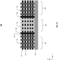
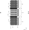
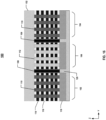
- FIGs. 11-16 illustrate cross-sections of 3D memory device 100 at different stages of a manufacturing process, according to some aspects of the present disclosure.
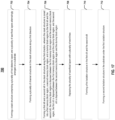
- FIG. 17 illustrates a flowchart of an exemplary method 700 for forming 3D memory device 100, according to some aspects of the present disclosure.
- the cross-sections of 3D memory device 100 in FIGs. 11-16 and method 700 in FIG. 17 will be discussed together. It is understood that the operations shown in method 700 are not exhaustive and that other operations may be performed as well before, after, or between any of the illustrated operations. Further, some of the operations may be performed simultaneously, or in a different order than shown in FIGs. 11-16 and FIG. 17 .
- a stack structure including a plurality of first dielectric layers 116 and a plurality of sacrificial layers 115 is formed on substrate 118.
- First dielectric layers 116 and sacrificial layers 115 are alternatingly arranged on substrate 118.
- the dielectric/sacrificial layer pairs may extend along the y-direction.
- each first dielectric layer 116 may include a layer of silicon oxide
- each sacrificial layer 115 may include a layer of silicon nitride.
- First dielectric layers 116 and sacrificial layers 115 may be formed by one or more thin film deposition processes including, but not limited to, chemical vapor deposition (CVD), physical vapor deposition (PVD), atomic layer deposition (ALD), or any combination thereof.
- CVD chemical vapor deposition
- PVD physical vapor deposition
- ALD atomic layer deposition
- a pad oxide layer (not shown) is formed between the substrate and the stack structure by depositing dielectric materials, such as silicon oxide, on the substrate.
- channel structures 110 and dummy channel structures 112 are formed in the stack structure along the z-direction.
- channel structures 110 and dummy channel structures 112 may have the same structure.
- Each channel structure 110 or dummy channel structure 112 may include a semiconductor channel and a memory film formed over the semiconductor channel.
- a channel hole is formed in the stack structure along the z-direction.
- an etch process may be performed to form the channel hole in the stack structure that extends vertically (z-direction) through the interleaved dielectric/sacrificial layers.
- fabrication processes for forming the channel hole may include wet etching and/or dry etching, such as deep reactive ion etching (DRIE).
- DRIE deep reactive ion etching
- the channel hole may extend further into the top portion of substrate 118. Then, a blocking layer, a storage layer, a tunneling layer, and a semiconductor channel may be sequentially formed in the channel hole.
- first slit 150 and a second slit 152 are formed in the stack structure along the y-direction.
- the stack structure is zoned into first memory region 102, second memory region 104, and dummy region 106 by first slit 150 and second slit 152.
- Dummy region 106 is disposed between first memory region 102 and second memory region 104.
- First slit 150 is disposed between first memory region 102 and dummy region 106
- second slit 152 is disposed between second memory region 104 and dummy region 106.
- first slit 150 and second slit 152 may be formed by dry etch, wet etch, or other suitable processes.
- the plurality of sacrificial layers 115 are replaced with the plurality of word lines (first conductive layers 114).
- sacrificial layers 115 may be removed by dry etch, wet etch, or other suitable processes to form a plurality of cavities.
- the word lines (first conductive layers 114) may be formed in the cavities by depositing the gate conductor, and the gate conductor made from tungsten.
- the cavities may be filled with the gate dielectric layer made from high-k dielectric materials, the adhesion layer including titanium/titanium nitride (Ti/TiN) or tantalum/tantalum nitride (Ta/TaN).
- first isolation structure 108 and second isolation structure 109 may be formed in first slit 150 and second slit 152. It is understood that first isolation structure 108 and second isolation structure 109 in FIG. 14 may be like or the same as first isolation structure 108 and second isolation structure 109 described above.
- a spacer 107 is formed along a sidewall of first slit 150 and second slit 152. In some implementations, spacer 107 may include one or multiple layers of dielectric films.
- a slit contact is formed by filling (e.g., depositing) conductive materials into the remaining space of first slit 150 and second slit 152 by PVD, CVD, ALD, any other suitable process, or any combination thereof.
- the slit contact may serve as a common source contact, according to some implementations.
- the slit contact may include conductive materials including, not limited to, W, Co, Cu, Al, polysilicon, silicides, or any combination thereof.
- a portion of substrate 118 is removed to form an opening 154.
- the portion of substrate 118 may be removed by dry etch, wet etch, or other suitable processes.
- a thinning operation may be further performed to thin substrate 118 and a carrier wafer 152 may be used during the thinning operation.
- third isolation structure 120 is formed in opening 154 under first isolation structure 108 and second isolation structure 109.
- third isolation structure 120 may be formed by dielectric material, and the dielectric material may also cover substrate 118.
- FIG. 18 illustrates a flowchart of another exemplary method 800 for forming 3D memory device 300, according to some aspects of the present disclosure.
- a stack structure including a plurality of first dielectric layers 116 and a plurality of sacrificial layers 115 is formed on substrate 118.
- First dielectric layers 116 and sacrificial layers 115 are alternatingly arranged on substrate 118.
- the dielectric/sacrificial layer pairs may extend along the x-direction.
- each first dielectric layer 116 may include a layer of silicon oxide
- each sacrificial layer 115 may include a layer of silicon nitride.
- First dielectric layers 116 and sacrificial layers 115 may be formed by one or more thin film deposition processes including, but not limited to, CVD, PVD, ALD, or any combination thereof.
- a pad oxide layer (not shown) is formed between the substrate and the stack structure by depositing dielectric materials, such as silicon oxide, on the substrate.
- channel structures 110 are formed in the stack structure along the y-direction.
- Each channel structure 110 may include a semiconductor channel and a memory film formed over the semiconductor channel.
- a channel hole is formed in the stack structure along the y-direction.
- an etch process may be performed to form the channel hole in the stack structure that extends vertically (y-direction) through the interleaved dielectric/sacrificial layers.
- fabrication processes for forming the channel hole may include wet etching and/or dry etching, such as DRIE.
- the channel hole may extend further into the top portion of substrate 118. Then, a blocking layer, a storage layer, a tunneling layer, and a semiconductor channel may be sequentially formed in the channel hole.
- a slit may be formed in the stack structure along the y-direction.
- the stack structure is zoned into first memory block region 102 and second memory block region 104 by the slit.
- the slit may be formed by dry etch, wet etch, or other suitable processes.
- the plurality of sacrificial layers 115 are replaced with the plurality of word lines (first conductive layers 114).
- sacrificial layers 115 may be removed by dry etch, wet etch, or other suitable processes to form a plurality of cavities.
- the word lines (first conductive layers 114) may be formed in the cavities by depositing the gate conductor, and the gate conductor made from tungsten.
- the cavities may be filled with the gate dielectric layer made from high-k dielectric materials, the adhesion layer including Ti/TiN or Ta/TaN.
- first isolation structure 108 may be formed in the slit.
- a spacer is formed along a sidewall of the slit.
- the spacer may include one or multiple layers of dielectric films.
- a slit contact is formed by filling (e.g., depositing) conductive materials into the remaining space of the slit by PVD, CVD, ALD, any other suitable process, or any combination thereof.
- the slit contact may serve as a common source contact, according to some implementations.
- the slit contact may include conductive materials including, not limited to, W, Co, Cu, Al, polysilicon, silicides, or any combination thereof.
- second isolation structure 120 is formed in opening 154 under first isolation structure 108.
- second isolation structure 120 may be formed by dielectric material, and the dielectric material may also cover substrate 118.
- first isolation structure 108 and second isolation structure 120 By forming first isolation structure 108 and second isolation structure 120 between first memory block region 102 and second memory block region 104, the word line (first conductive layers 114) of different memory stacks may be isolated, and the well regions of substrate 118 under different memory stacks can also be electrically isolated without a complicated structure.
- FIG. 19 illustrates a block diagram of an exemplary system 900 having a memory device, according to some aspects of the present disclosure.
- System 900 can be a mobile phone, a desktop computer, a laptop computer, a tablet, a vehicle computer, a gaming console, a printer, a positioning device, a wearable electronic device, a smart sensor, a virtual reality (VR) device, an argument reality (AR) device, or any other suitable electronic devices having storage therein.
- system 900 can include a host 908 and a memory system 902 having one or more memory devices 904 and a memory controller 906.
- Host 908 can be a processor of an electronic device, such as a central processing unit (CPU), or a system-on-chip (SoC), such as an application processor (AP). Host 908 can be configured to send or receive data to or from memory devices 904.
- CPU central processing unit
- SoC system-on-chip
- AP application processor
- Host 908 can be configured to send or receive data to or from memory devices 904.
- Memory device 904 can be any memory device disclosed in the present disclosure. As disclosed above in detail, memory device 904, such as a NAND Flash memory device, may have a controlled and predefined discharge current in the discharge operation of discharging the bit lines.
- Memory controller 906 is coupled to memory device 904 and host 908 and is configured to control memory device 904, according to some implementations. Memory controller 906 can manage the data stored in memory device 904 and communicate with host 908. For example, memory controller 906 may be coupled to memory device 904, such as 3D memory device 100 described above, and memory controller 906 may be configured to control the operations of channel structure 110 through the peripheral device. By forming the structure according to the present disclosure, the area of 3D memory device 100 may be reduced by using the first isolation structures disclosed.
- memory controller 906 is designed for operating in a low duty-cycle environment like secure digital (SD) cards, compact Flash (CF) cards, universal serial bus (USB) Flash drives, or other media for use in electronic devices, such as personal computers, digital cameras, mobile phones, etc.
- memory controller 906 is designed for operating in a high duty-cycle environment SSDs or embedded multi-media-cards (eMMCs) used as data storage for mobile devices, such as smartphones, tablets, laptop computers, etc., and enterprise storage arrays.
- Memory controller 906 can be configured to control operations of memory device 904, such as read, erase, and program operations.
- Memory controller 906 can also be configured to manage various functions with respect to the data stored or to be stored in memory device 904 including, but not limited to bad-block management, garbage collection, logical-to-physical address conversion, wear leveling, etc. In some implementations, memory controller 906 is further configured to process error correction codes (ECCs) with respect to the data read from or written to memory device 904. Any other suitable functions may be performed by memory controller 906 as well, for example, formatting memory device 904. Memory controller 906 can communicate with an external device (e.g., host 908) according to a particular communication protocol.
- ECCs error correction codes
- memory controller 906 may communicate with the external device through at least one of various interface protocols, such as a USB protocol, an MMC protocol, a peripheral component interconnection (PCI) protocol, a PCI-express (PCI-E) protocol, an advanced technology attachment (ATA) protocol, a serial-ATA protocol, a parallel-ATA protocol, a small computer small interface (SCSI) protocol, an enhanced small disk interface (ESDI) protocol, an integrated drive electronics (IDE) protocol, a Firewire protocol, etc.
- various interface protocols such as a USB protocol, an MMC protocol, a peripheral component interconnection (PCI) protocol, a PCI-express (PCI-E) protocol, an advanced technology attachment (ATA) protocol, a serial-ATA protocol, a parallel-ATA protocol, a small computer small interface (SCSI) protocol, an enhanced small disk interface (ESDI) protocol, an integrated drive electronics (IDE) protocol, a Firewire protocol, etc.
- various interface protocols such as a USB protocol, an MMC protocol, a peripheral component interconnection (
- Memory controller 906 and one or more memory devices 904 can be integrated into various types of storage devices, for example, be included in the same package, such as a universal Flash storage (UFS) package or an eMMC package. That is, memory system 902 can be implemented and packaged into different types of end electronic products. In one example as shown in FIG. 20A , memory controller 906 and a single memory device 904 may be integrated into a memory card 1002.
- Memory card 1002 can include a PC card (PCMCIA, personal computer memory card international association), a CF card, a smart media (SM) card, a memory stick, a multimedia card (MMC, RS-MMC, MMCmicro), an SD card (SD, miniSD, microSD, SDHC), a UFS, etc.
- Memory card 1002 can further include a memory card connector 1004 coupling memory card 1002 with a host (e.g., host 908 in FIG. 19 ).
- memory controller 906 and multiple memory devices 904 may be integrated into an SSD 1006.
- SSD 1006 can further include an SSD connector 1008 coupling SSD 1006 with a host (e.g., host 908 in FIG. 19 ).
- the storage capacity and/or the operation speed of SSD 1006 is greater than those of memory card 1002.
Landscapes
- Semiconductor Memories (AREA)
- Non-Volatile Memory (AREA)
Claims (13)
- Dreidimensionale (3D) Speichervorrichtung (100, 200, 300, 400, 500, 600), die Folgendes aufweist:eine Vielzahl von Speicherstapeln, die einen ersten Speicherstapel und einen zweiten Speicherstapel aufweisen, die entlang einer ersten Richtung angeordnet sind, wobei jeder Speicherstapel Folgendes aufweist:eine Vielzahl von ersten leitenden Schichten (114) und eine Vielzahl von ersten dielektrischen Schichten (116), die abwechselnd entlang einer zweiten Richtung senkrecht zu der ersten Richtung gestapelt sind; undeine Kanalstruktur (110), die sich durch die Vielzahl von ersten leitenden Schichten (114) und die Vielzahl von ersten dielektrischen Schichten (116) entlang der zweiten Richtung erstreckt;eine Dummy-Struktur, die zwischen dem ersten Speicherstapel und dem zweiten Speicherstapel angeordnet ist, wobei sich die Dummy-Struktur entlang einer zweiten Richtung senkrecht zu der ersten Richtung und einer dritten Richtung senkrecht zu der ersten Richtung und zu der zweiten Richtung erstreckt;eine erste Isolationsstruktur (108), die zwischen der Dummy-Struktur und dem ersten Speicherstapel angeordnet ist, wobei sich die erste Isolationsstruktur (108) entlang der zweiten Richtung und der dritten Richtung erstreckt;eine zweite Isolationsstruktur (109), die zwischen der Dummy-Struktur und dem zweiten Speicherstapel angeordnet ist, wobei sich die zweite Isolationsstruktur (109) entlang der zweiten Richtung und der dritten Richtung erstreckt;eine Halbleiterschicht, die unter der Vielzahl von Speicherstapeln, der Dummy-Struktur, der ersten Isolationsstruktur (108) und der zweiten Isolationsstruktur (109) angeordnet ist; undeine Grabenisolationsstruktur, die in der Halbleiterschicht angeordnet ist, die sich entlang der zweiten Richtung und der dritten Richtung erstreckt, wobei die Grabenisolationsstruktur die Halbleiterschicht unter jedem Speicherstapel elektrisch isoliert und wobei die Grabenisolationsstruktur unter der ersten und der zweiten Isolationsstruktur (109) angeordnet ist und zu der ersten und der zweiten Isolationsstruktur (109) ausgerichtet ist.
- 3D-Speichervorrichtung (100, 200, 300, 400, 500, 600) nach Anspruch 1,wobei die Dummy-Struktur eine Vielzahl von zweiten leitenden Schichten und eine Vielzahl von zweiten dielektrischen Schichten aufweist, die abwechselnd entlang der zweiten Richtung gestapelt sind,wobei insbesondere die Vielzahl erster leitender Schichten (114) und die Vielzahl zweiter leitender Schichten dasselbe leitende Material aufweisen, und die Vielzahl erster dielektrischer Schichten (116) und die Vielzahl zweiter dielektrischer Schichten dasselbe dielektrische Material aufweisen.
- 3D-Speichervorrichtung (100, 200, 300, 400, 500, 600) nach Anspruch 2,
wobei die Dummy-Struktur ferner eine Dummy-Kanalstruktur (112) aufweist, die sich durch die Vielzahl von zweiten leitenden Schichten und die Vielzahl von zweiten dielektrischen Schichten entlang der zweiten Richtung erstreckt, wobei die Dummy-Kanalstruktur (112) einen Halbleiterkanal und einen über dem Halbleiterkanal ausgebildeten Speicherfilm aufweist. - 3D-Speichervorrichtung (100, 200, 300, 400, 500, 600) nach Anspruch 2,
wobei die Dummy-Struktur ferner eine Kontaktstruktur (412) aufweist, die sich durch die Vielzahl von zweiten leitenden Schichten und die Vielzahl von zweiten dielektrischen Schichten entlang der zweiten Richtung erstreckt. - 3D-Speichervorrichtung (100, 200, 300, 400, 500, 600) nach Anspruch 4, wobei die Kontaktstruktur (412) ferner Folgendes aufweist:einen Kontakt, der sich durch die Vielzahl von zweiten leitenden Schichten und die Vielzahl von zweiten dielektrischen Schichten entlang der zweiten Richtung erstreckt; undeine dritte dielektrische Schicht, die sich entlang der zweiten Richtung erstreckt und den Kontakt umgibt.
- 3D-Speichervorrichtung (100, 200, 300, 400, 500, 600) nach Anspruch 5, die ferner Folgendes aufweist:
eine dritte leitende Schicht, die in der Halbleiterschicht angeordnet ist und sich entlang der zweiten Richtung unter dem Kontakt erstreckt, wobei die dritte leitende Schicht elektrisch mit dem Kontakt verbunden ist und von einer dritten dielektrischen Schicht umgeben ist, wobei insbesondere der Kontakt und die dritte leitende Schicht elektrisch mit einer Peripherievorrichtung verbunden sind. - 3D-Speichervorrichtung (100, 200, 300, 400, 500, 600) nach einem der Ansprüche 1 bis 6, wobei die erste Isolationsstruktur (108) ferner einen Gate-Leitungsschlitz aufweist, der sich entlang der zweiten Richtung und der dritten Richtung erstreckt,
wobei insbesondere die erste Isolationsstruktur (108) die Vielzahl von ersten leitenden Schichten (114) und die Vielzahl von zweiten leitenden Schichten elektrisch isoliert. - System (900) mit:einer dreidimensionalen (3D) Speichervorrichtung (100, 200, 300, 400, 500, 600) gemäß einem der Ansprüche 1-7 undeinem Speicher-Controller (906), der mit der 3D-Speichervorrichtung (100, 200, 300, 400, 500, 600) gekoppelt ist und so konfiguriert ist, dass er die Operationen der 3D-Speichervorrichtung (100, 200, 300, 400, 500, 600) steuert.
- Verfahren (700, 800) zum Herstellen einer dreidimensionalen (3D) Speichervorrichtung (100, 200, 300, 400, 500, 600), das folgende Schritte aufweist:Bilden einer Stapelstruktur, die eine Vielzahl von ersten dielektrischen Schichten (116) und eine Vielzahl von Opferschichten (115) aufweist, die abwechselnd auf einer Halbleiterschicht angeordnet sind, wobei die Stapelstruktur eine Vielzahl von dielektrischen Stapeln aufweist, die entlang einer ersten Richtung angeordnet sind;Bilden einer Vielzahl von Kanalstrukturen (110) in der Stapelstruktur entlang einer zweiten Richtung, die senkrecht zu der ersten Richtung ist;Bilden einer ersten Öffnung und einer zweiten Öffnung in der Stapelstruktur von einer oberen Seite der Stapelstruktur entlang der zweiten Richtung und einer dritten Richtung, die senkrecht zu der ersten Richtung und der zweiten Richtung ist, wobei die Vielzahl von dielektrischen Stapeln in einen ersten Speicherbereich (102), einen zweiten Speicherbereich (104) und einen Dummy-Bereich (106 , 406, 506, 606) durch die erste Öffnung und die zweite Öffnung unterteilt sind, wobei der Dummy-Bereich (106, 406, 506, 606) zwischen dem ersten Speicherbereich (102) und dem zweiten Speicherbereich (104) angeordnet ist, wobei die erste Öffnung zwischen dem ersten Speicherbereich (102) und dem Dummy-Bereich (106, 406, 506, 606) angeordnet ist und die zweite Öffnung zwischen dem zweiten Speicherbereich (104) und dem Dummy-Bereich (106, 406, 506, 606) angeordnet ist;Ersetzen der Vielzahl von Opferschichten (115) durch eine Vielzahl von leitenden Schichten;Bilden einer ersten Isolationsstruktur (108) in der ersten Öffnung und einer zweiten Isolationsstruktur (109) in der zweiten Öffnung; undBilden einer dritten Isolationsstruktur (120) in der Halbleiterschicht unter der ersten Isolationsstruktur (108) und Bilden einer vierten Isolationsstruktur (220) in der Halbleiterschicht unter der zweiten Isolationsstruktur (109), wobei die Grabenisolationsstruktur die Halbleiterschicht unter jedem Speicherstapel elektrisch isoliert und wobei die Grabenisolationsstruktur unter der ersten und der zweiten Isolationsstruktur (109) angeordnet ist und zu der ersten und der zweiten Isolationsstruktur (109) ausgerichtet ist.
- Verfahren (700, 800) nach Anspruch 9, wobei das Bilden der Vielzahl von Kanalstrukturen (110) in der Stapelstruktur entlang der zweiten Richtung ferner folgende Schritte aufweist:Bilden der Vielzahl von Kanalstrukturen (110) in dem ersten Speicherbereich (102), dem zweiten Speicherbereich (104) und dem Dummy-Bereich (106, 406, 506, 606) entlang der zweiten Richtung oderBilden der Vielzahl von Kanalstrukturen (110) in dem ersten Speicherbereich (102) und dem zweiten Speicherbereich (104); undBilden einer Kontaktstruktur (412) in dem Dummy-Bereich (106, 406, 506, 606) entlang der zweiten Richtung.
- Verfahren (700, 800) nach einem der Ansprüche 9 bis 10, wobei das Bilden der ersten Isolationsstruktur (108) in der ersten Öffnung und der zweiten Isolationsstruktur (109) in der zweiten Öffnung ferner folgenden Schritt aufweist:Bilden einer ersten Gate-Leitungsschlitzstruktur in der ersten Öffnung und einer zweiten Gate-Leitungsschlitzstruktur in der zweiten Öffnung,wobei das Verfahren (700, 800) insbesondere ferner das Bilden einer zweiten dielektrischen Schicht in der ersten Öffnung und einer dritten dielektrischen Schicht in der zweiten Öffnung aufweist.
- Verfahren (700, 800) nach einem der Ansprüche 9 bis 11, wobei das Bilden der dritten Isolationsstruktur (120) in der Halbleiterschicht unter der ersten Isolationsstruktur (108) und das Bilden der vierten Isolationsstruktur (220) in der Halbleiterschicht unter der zweiten Isolationsstruktur (109) ferner folgende Schritte aufweist:Bilden einer dritten Öffnung in der Halbleiterschicht unter der ersten Isolationsstruktur (108) und der zweiten Isolationsstruktur (109) von einer Seite der Halbleiterschicht, die von der Stapelstruktur entfernt ist; undBilden einer vierten dielektrischen Schicht in der dritten Öffnung.
- Verfahren (700, 800) nach einem der Ansprüche 9 bis 12, wobei die erste Isolationsstruktur (108) die Vielzahl leitender Schichten zwischen dem ersten Speicherbereich (102) und dem Dummy-Bereich (106, 40 6, 506, 606) elektrisch isoliert und die zweite Isolationsstruktur (109) die Vielzahl leitender Schichten zwischen dem zweiten Speicherbereich (104) und dem Dummy-Bereich (106, 406, 506, 606) elektrisch isoliert,
wobei insbesondere die dritte Isolationsstruktur (120) die Halbleiterschicht unter dem ersten Speicherbereich (102) und dem Dummy-Bereich (106, 406, 506, 606) elektrisch isoliert, und die vierte Isolationsstruktur (220) die Halbleiterschicht unter dem zweiten Speicherbereich (104) und dem Dummy-Bereich (106, 406, 506, 606) elektrisch isoliert.
Priority Applications (1)
| Application Number | Priority Date | Filing Date | Title |
|---|---|---|---|
| EP25153596.9A EP4525581A1 (de) | 2021-11-18 | 2022-06-01 | Dreidimensionale speichervorrichtung und verfahren zur herstellung davon |
Applications Claiming Priority (4)
| Application Number | Priority Date | Filing Date | Title |
|---|---|---|---|
| CN202111371139.3A CN114038861B (zh) | 2021-11-18 | 2021-11-18 | 一种3d nand存储器件及其制造方法 |
| CN202111369252.8A CN114038860B (zh) | 2021-11-18 | 2021-11-18 | 一种3d nand存储器件及其制造方法 |
| CN202111369255.1A CN114093811B (zh) | 2021-11-18 | 2021-11-18 | 一种3d nand存储器件及其制造方法 |
| PCT/CN2022/096598 WO2023087666A1 (en) | 2021-11-18 | 2022-06-01 | Three-dimensional memory device and method for forming the same |
Related Child Applications (1)
| Application Number | Title | Priority Date | Filing Date |
|---|---|---|---|
| EP25153596.9A Division EP4525581A1 (de) | 2021-11-18 | 2022-06-01 | Dreidimensionale speichervorrichtung und verfahren zur herstellung davon |
Publications (3)
| Publication Number | Publication Date |
|---|---|
| EP4205175A1 EP4205175A1 (de) | 2023-07-05 |
| EP4205175A4 EP4205175A4 (de) | 2024-01-17 |
| EP4205175B1 true EP4205175B1 (de) | 2025-02-19 |
Family
ID=86323440
Family Applications (2)
| Application Number | Title | Priority Date | Filing Date |
|---|---|---|---|
| EP22817512.1A Active EP4205175B1 (de) | 2021-11-18 | 2022-06-01 | Dreidimensionale speichervorrichtung und verfahren zur herstellung davon |
| EP25153596.9A Pending EP4525581A1 (de) | 2021-11-18 | 2022-06-01 | Dreidimensionale speichervorrichtung und verfahren zur herstellung davon |
Family Applications After (1)
| Application Number | Title | Priority Date | Filing Date |
|---|---|---|---|
| EP25153596.9A Pending EP4525581A1 (de) | 2021-11-18 | 2022-06-01 | Dreidimensionale speichervorrichtung und verfahren zur herstellung davon |
Country Status (4)
| Country | Link |
|---|---|
| US (2) | US12389603B2 (de) |
| EP (2) | EP4205175B1 (de) |
| KR (2) | KR102764859B1 (de) |
| CN (1) | CN116508409A (de) |
Families Citing this family (2)
| Publication number | Priority date | Publication date | Assignee | Title |
|---|---|---|---|---|
| US12501616B2 (en) * | 2022-09-23 | 2025-12-16 | Yangtze Memory Technologies Co., Ltd. | Memory system, semiconductor device and fabrication method therefor |
| WO2025007290A1 (en) * | 2023-07-05 | 2025-01-09 | Yangtze Memory Technologies Co., Ltd. | Three-dimensional memory device utilizing dummy memory blocks to mitigate defects |
Family Cites Families (12)
| Publication number | Priority date | Publication date | Assignee | Title |
|---|---|---|---|---|
| KR20160138765A (ko) | 2015-05-26 | 2016-12-06 | 에스케이하이닉스 주식회사 | 슬리밍 구조물을 포함하는 반도체 메모리 장치 |
| KR102565716B1 (ko) | 2015-12-24 | 2023-08-11 | 삼성전자주식회사 | 메모리 장치 |
| KR102530757B1 (ko) | 2016-01-18 | 2023-05-11 | 삼성전자주식회사 | 메모리 장치 |
| KR20250025029A (ko) * | 2017-03-08 | 2025-02-20 | 양쯔 메모리 테크놀로지스 씨오., 엘티디. | 3차원 메모리 장치의 쓰루 어레이 컨택 구조 |
| CN106910746B (zh) | 2017-03-08 | 2018-06-19 | 长江存储科技有限责任公司 | 一种3d nand存储器件及其制造方法、封装方法 |
| KR102789287B1 (ko) | 2019-05-03 | 2025-04-01 | 삼성전자주식회사 | 반도체 장치 및 이의 제조 방법 |
| KR102815714B1 (ko) | 2019-07-24 | 2025-06-02 | 삼성전자주식회사 | 수직형 메모리 소자 및 이의 제조방법 |
| KR102717037B1 (ko) | 2019-11-01 | 2024-10-15 | 에스케이하이닉스 주식회사 | 반도체 메모리 장치 및 그 제조방법 |
| EP4101005A4 (de) * | 2020-02-08 | 2023-10-11 | INTEL Corporation | Block-zu-block-isolation und tiefenkontakt unter verwendung von säulen in einer speichermatrix |
| CN114038860B (zh) | 2021-11-18 | 2026-04-14 | 长江存储科技有限责任公司 | 一种3d nand存储器件及其制造方法 |
| CN114093811B (zh) | 2021-11-18 | 2026-03-27 | 长江存储科技有限责任公司 | 一种3d nand存储器件及其制造方法 |
| CN114038861B (zh) | 2021-11-18 | 2026-04-14 | 长江存储科技有限责任公司 | 一种3d nand存储器件及其制造方法 |
-
2022
- 2022-06-01 KR KR1020227044746A patent/KR102764859B1/ko active Active
- 2022-06-01 EP EP22817512.1A patent/EP4205175B1/de active Active
- 2022-06-01 CN CN202280002313.3A patent/CN116508409A/zh active Pending
- 2022-06-01 EP EP25153596.9A patent/EP4525581A1/de active Pending
- 2022-06-01 KR KR1020257002718A patent/KR20250022224A/ko active Pending
- 2022-06-22 US US17/846,612 patent/US12389603B2/en active Active
-
2025
- 2025-06-26 US US19/251,610 patent/US20250324604A1/en active Pending
Also Published As
| Publication number | Publication date |
|---|---|
| KR20250022224A (ko) | 2025-02-14 |
| KR20230074415A (ko) | 2023-05-30 |
| KR102764859B1 (ko) | 2025-02-06 |
| EP4205175A1 (de) | 2023-07-05 |
| EP4525581A1 (de) | 2025-03-19 |
| EP4205175A4 (de) | 2024-01-17 |
| CN116508409A (zh) | 2023-07-28 |
| US20230157027A1 (en) | 2023-05-18 |
| US20250324604A1 (en) | 2025-10-16 |
| US12389603B2 (en) | 2025-08-12 |
Similar Documents
| Publication | Publication Date | Title |
|---|---|---|
| EP4367666B1 (de) | Dreidimensionale speichervorrichtungen und verfahren zur formung davon | |
| US20250324604A1 (en) | Three-dimensional memory device and method for forming the same | |
| US20250089256A1 (en) | Three-dimensional memory device and method for forming the same | |
| US20250056804A1 (en) | Three-dimensional memory device with improved charge lateral migration and method for forming the same | |
| US20260122902A1 (en) | Three-dimensional memory device with divided drain select gate lines and method for forming the same | |
| US20250240954A1 (en) | Three-dimensional memory device with divided drain select gate lines and method for forming the same | |
| US20230225124A1 (en) | Three-dimensional memory devices and methods for forming the same | |
| US12075621B2 (en) | Three-dimensional memory device and method for forming the same | |
| WO2023087666A1 (en) | Three-dimensional memory device and method for forming the same | |
| US20240063140A1 (en) | Three-dimensional memory devices, systems, and methods for forming the same | |
| US12615772B2 (en) | Three-dimensional memory devices and methods for forming the same | |
| US12193233B2 (en) | Three-dimensional memory device with restrained charge migration and method for forming the same | |
| US20240064978A1 (en) | Three-dimensional memory devices, systems, and methods for forming the same | |
| US20230413570A1 (en) | Three-dimensional memory device and method for forming the same | |
| US20240098989A1 (en) | Three-dimensional memory devices and methods for forming the same | |
| US12598748B2 (en) | Three-dimensional memory devices and methods for forming the same | |
| WO2022083299A1 (en) | Three-dimensional memory device and method for forming the same |
Legal Events
| Date | Code | Title | Description |
|---|---|---|---|
| STAA | Information on the status of an ep patent application or granted ep patent |
Free format text: STATUS: UNKNOWN |
|
| STAA | Information on the status of an ep patent application or granted ep patent |
Free format text: STATUS: THE INTERNATIONAL PUBLICATION HAS BEEN MADE |
|
| PUAI | Public reference made under article 153(3) epc to a published international application that has entered the european phase |
Free format text: ORIGINAL CODE: 0009012 |
|
| STAA | Information on the status of an ep patent application or granted ep patent |
Free format text: STATUS: REQUEST FOR EXAMINATION WAS MADE |
|
| 17P | Request for examination filed |
Effective date: 20221216 |
|
| AK | Designated contracting states |
Kind code of ref document: A1 Designated state(s): AL AT BE BG CH CY CZ DE DK EE ES FI FR GB GR HR HU IE IS IT LI LT LU LV MC MK MT NL NO PL PT RO RS SE SI SK SM TR |
|
| REG | Reference to a national code |
Ref legal event code: R079 Free format text: PREVIOUS MAIN CLASS: H01L0027115820 Ref country code: DE Ref legal event code: R079 Ref document number: 602022010935 Country of ref document: DE Free format text: PREVIOUS MAIN CLASS: H01L0027115820 Ipc: H10B0043100000 |
|
| A4 | Supplementary search report drawn up and despatched |
Effective date: 20231220 |
|
| RIC1 | Information provided on ipc code assigned before grant |
Ipc: H10B 43/50 20230101ALI20231214BHEP Ipc: H10B 43/27 20230101ALI20231214BHEP Ipc: H10B 43/10 20230101AFI20231214BHEP |
|
| STAA | Information on the status of an ep patent application or granted ep patent |
Free format text: STATUS: EXAMINATION IS IN PROGRESS |
|
| 17Q | First examination report despatched |
Effective date: 20240607 |
|
| GRAP | Despatch of communication of intention to grant a patent |
Free format text: ORIGINAL CODE: EPIDOSNIGR1 |
|
| STAA | Information on the status of an ep patent application or granted ep patent |
Free format text: STATUS: GRANT OF PATENT IS INTENDED |
|
| DAV | Request for validation of the european patent (deleted) | ||
| DAX | Request for extension of the european patent (deleted) | ||
| INTG | Intention to grant announced |
Effective date: 20241028 |
|
| RIN1 | Information on inventor provided before grant (corrected) |
Inventor name: WANG, YANHONG Inventor name: LIU, WEI Inventor name: HUANG, SHIQI Inventor name: CHEN, LIANG |
|
| GRAS | Grant fee paid |
Free format text: ORIGINAL CODE: EPIDOSNIGR3 |
|
| GRAA | (expected) grant |
Free format text: ORIGINAL CODE: 0009210 |
|
| STAA | Information on the status of an ep patent application or granted ep patent |
Free format text: STATUS: THE PATENT HAS BEEN GRANTED |
|
| AK | Designated contracting states |
Kind code of ref document: B1 Designated state(s): AL AT BE BG CH CY CZ DE DK EE ES FI FR GB GR HR HU IE IS IT LI LT LU LV MC MK MT NL NO PL PT RO RS SE SI SK SM TR |
|
| REG | Reference to a national code |
Ref country code: GB Ref legal event code: FG4D |
|
| REG | Reference to a national code |
Ref country code: CH Ref legal event code: EP |
|
| REG | Reference to a national code |
Ref country code: IE Ref legal event code: FG4D |
|
| REG | Reference to a national code |
Ref country code: DE Ref legal event code: R096 Ref document number: 602022010935 Country of ref document: DE |
|
| P01 | Opt-out of the competence of the unified patent court (upc) registered |
Free format text: CASE NUMBER: APP_7543/2025 Effective date: 20250213 |
|
| REG | Reference to a national code |
Ref country code: NL Ref legal event code: MP Effective date: 20250219 |
|
| PG25 | Lapsed in a contracting state [announced via postgrant information from national office to epo] |
Ref country code: RS Free format text: LAPSE BECAUSE OF FAILURE TO SUBMIT A TRANSLATION OF THE DESCRIPTION OR TO PAY THE FEE WITHIN THE PRESCRIBED TIME-LIMIT Effective date: 20250519 |
|
| PG25 | Lapsed in a contracting state [announced via postgrant information from national office to epo] |
Ref country code: FI Free format text: LAPSE BECAUSE OF FAILURE TO SUBMIT A TRANSLATION OF THE DESCRIPTION OR TO PAY THE FEE WITHIN THE PRESCRIBED TIME-LIMIT Effective date: 20250219 |
|
| PG25 | Lapsed in a contracting state [announced via postgrant information from national office to epo] |
Ref country code: PL Free format text: LAPSE BECAUSE OF FAILURE TO SUBMIT A TRANSLATION OF THE DESCRIPTION OR TO PAY THE FEE WITHIN THE PRESCRIBED TIME-LIMIT Effective date: 20250219 |
|
| PGFP | Annual fee paid to national office [announced via postgrant information from national office to epo] |
Ref country code: DE Payment date: 20250618 Year of fee payment: 4 |
|
| PG25 | Lapsed in a contracting state [announced via postgrant information from national office to epo] |
Ref country code: ES Free format text: LAPSE BECAUSE OF FAILURE TO SUBMIT A TRANSLATION OF THE DESCRIPTION OR TO PAY THE FEE WITHIN THE PRESCRIBED TIME-LIMIT Effective date: 20250219 |
|
| REG | Reference to a national code |
Ref country code: LT Ref legal event code: MG9D |
|
| PG25 | Lapsed in a contracting state [announced via postgrant information from national office to epo] |
Ref country code: IS Free format text: LAPSE BECAUSE OF FAILURE TO SUBMIT A TRANSLATION OF THE DESCRIPTION OR TO PAY THE FEE WITHIN THE PRESCRIBED TIME-LIMIT Effective date: 20250619 Ref country code: NO Free format text: LAPSE BECAUSE OF FAILURE TO SUBMIT A TRANSLATION OF THE DESCRIPTION OR TO PAY THE FEE WITHIN THE PRESCRIBED TIME-LIMIT Effective date: 20250519 |
|
| PG25 | Lapsed in a contracting state [announced via postgrant information from national office to epo] |
Ref country code: NL Free format text: LAPSE BECAUSE OF FAILURE TO SUBMIT A TRANSLATION OF THE DESCRIPTION OR TO PAY THE FEE WITHIN THE PRESCRIBED TIME-LIMIT Effective date: 20250219 |
|
| PG25 | Lapsed in a contracting state [announced via postgrant information from national office to epo] |
Ref country code: HR Free format text: LAPSE BECAUSE OF FAILURE TO SUBMIT A TRANSLATION OF THE DESCRIPTION OR TO PAY THE FEE WITHIN THE PRESCRIBED TIME-LIMIT Effective date: 20250219 |
|
| PG25 | Lapsed in a contracting state [announced via postgrant information from national office to epo] |
Ref country code: LV Free format text: LAPSE BECAUSE OF FAILURE TO SUBMIT A TRANSLATION OF THE DESCRIPTION OR TO PAY THE FEE WITHIN THE PRESCRIBED TIME-LIMIT Effective date: 20250219 Ref country code: PT Free format text: LAPSE BECAUSE OF FAILURE TO SUBMIT A TRANSLATION OF THE DESCRIPTION OR TO PAY THE FEE WITHIN THE PRESCRIBED TIME-LIMIT Effective date: 20250620 |
|
| PGFP | Annual fee paid to national office [announced via postgrant information from national office to epo] |
Ref country code: FR Payment date: 20250522 Year of fee payment: 4 |
|
| PG25 | Lapsed in a contracting state [announced via postgrant information from national office to epo] |
Ref country code: BG Free format text: LAPSE BECAUSE OF FAILURE TO SUBMIT A TRANSLATION OF THE DESCRIPTION OR TO PAY THE FEE WITHIN THE PRESCRIBED TIME-LIMIT Effective date: 20250219 Ref country code: GR Free format text: LAPSE BECAUSE OF FAILURE TO SUBMIT A TRANSLATION OF THE DESCRIPTION OR TO PAY THE FEE WITHIN THE PRESCRIBED TIME-LIMIT Effective date: 20250520 |
|
| REG | Reference to a national code |
Ref country code: AT Ref legal event code: MK05 Ref document number: 1769656 Country of ref document: AT Kind code of ref document: T Effective date: 20250219 |
|
| PG25 | Lapsed in a contracting state [announced via postgrant information from national office to epo] |
Ref country code: SE Free format text: LAPSE BECAUSE OF FAILURE TO SUBMIT A TRANSLATION OF THE DESCRIPTION OR TO PAY THE FEE WITHIN THE PRESCRIBED TIME-LIMIT Effective date: 20250219 |
|
| PG25 | Lapsed in a contracting state [announced via postgrant information from national office to epo] |
Ref country code: SM Free format text: LAPSE BECAUSE OF FAILURE TO SUBMIT A TRANSLATION OF THE DESCRIPTION OR TO PAY THE FEE WITHIN THE PRESCRIBED TIME-LIMIT Effective date: 20250219 |
|
| PG25 | Lapsed in a contracting state [announced via postgrant information from national office to epo] |
Ref country code: DK Free format text: LAPSE BECAUSE OF FAILURE TO SUBMIT A TRANSLATION OF THE DESCRIPTION OR TO PAY THE FEE WITHIN THE PRESCRIBED TIME-LIMIT Effective date: 20250219 |
|
| PG25 | Lapsed in a contracting state [announced via postgrant information from national office to epo] |
Ref country code: IT Free format text: LAPSE BECAUSE OF FAILURE TO SUBMIT A TRANSLATION OF THE DESCRIPTION OR TO PAY THE FEE WITHIN THE PRESCRIBED TIME-LIMIT Effective date: 20250219 |
|
| PG25 | Lapsed in a contracting state [announced via postgrant information from national office to epo] |
Ref country code: AT Free format text: LAPSE BECAUSE OF FAILURE TO SUBMIT A TRANSLATION OF THE DESCRIPTION OR TO PAY THE FEE WITHIN THE PRESCRIBED TIME-LIMIT Effective date: 20250219 |
|
| PG25 | Lapsed in a contracting state [announced via postgrant information from national office to epo] |
Ref country code: EE Free format text: LAPSE BECAUSE OF FAILURE TO SUBMIT A TRANSLATION OF THE DESCRIPTION OR TO PAY THE FEE WITHIN THE PRESCRIBED TIME-LIMIT Effective date: 20250219 Ref country code: CZ Free format text: LAPSE BECAUSE OF FAILURE TO SUBMIT A TRANSLATION OF THE DESCRIPTION OR TO PAY THE FEE WITHIN THE PRESCRIBED TIME-LIMIT Effective date: 20250219 |
|
| PG25 | Lapsed in a contracting state [announced via postgrant information from national office to epo] |
Ref country code: RO Free format text: LAPSE BECAUSE OF FAILURE TO SUBMIT A TRANSLATION OF THE DESCRIPTION OR TO PAY THE FEE WITHIN THE PRESCRIBED TIME-LIMIT Effective date: 20250219 |
|
| PG25 | Lapsed in a contracting state [announced via postgrant information from national office to epo] |
Ref country code: SK Free format text: LAPSE BECAUSE OF FAILURE TO SUBMIT A TRANSLATION OF THE DESCRIPTION OR TO PAY THE FEE WITHIN THE PRESCRIBED TIME-LIMIT Effective date: 20250219 |
|
| REG | Reference to a national code |
Ref country code: DE Ref legal event code: R097 Ref document number: 602022010935 Country of ref document: DE |
|
| PLBE | No opposition filed within time limit |
Free format text: ORIGINAL CODE: 0009261 |
|
| STAA | Information on the status of an ep patent application or granted ep patent |
Free format text: STATUS: NO OPPOSITION FILED WITHIN TIME LIMIT |
|
| REG | Reference to a national code |
Ref country code: CH Ref legal event code: L10 Free format text: ST27 STATUS EVENT CODE: U-0-0-L10-L00 (AS PROVIDED BY THE NATIONAL OFFICE) Effective date: 20251231 |
|
| REG | Reference to a national code |
Ref country code: CH Ref legal event code: H13 Free format text: ST27 STATUS EVENT CODE: U-0-0-H10-H13 (AS PROVIDED BY THE NATIONAL OFFICE) Effective date: 20260127 |
|
| 26N | No opposition filed |
Effective date: 20251120 |
|
| PG25 | Lapsed in a contracting state [announced via postgrant information from national office to epo] |
Ref country code: MC Free format text: LAPSE BECAUSE OF FAILURE TO SUBMIT A TRANSLATION OF THE DESCRIPTION OR TO PAY THE FEE WITHIN THE PRESCRIBED TIME-LIMIT Effective date: 20250219 |
|
| PG25 | Lapsed in a contracting state [announced via postgrant information from national office to epo] |
Ref country code: LU Free format text: LAPSE BECAUSE OF NON-PAYMENT OF DUE FEES Effective date: 20250601 |
|
| REG | Reference to a national code |
Ref country code: BE Ref legal event code: MM Effective date: 20250630 |
|
| PG25 | Lapsed in a contracting state [announced via postgrant information from national office to epo] |
Ref country code: IE Free format text: LAPSE BECAUSE OF NON-PAYMENT OF DUE FEES Effective date: 20250601 |
|
| PG25 | Lapsed in a contracting state [announced via postgrant information from national office to epo] |
Ref country code: BE Free format text: LAPSE BECAUSE OF NON-PAYMENT OF DUE FEES Effective date: 20250630 |
|
| PG25 | Lapsed in a contracting state [announced via postgrant information from national office to epo] |
Ref country code: CH Free format text: LAPSE BECAUSE OF NON-PAYMENT OF DUE FEES Effective date: 20250630 |