EP4203313A1 - Pulse signal generation circuit and generation method, and memory - Google Patents
Pulse signal generation circuit and generation method, and memory Download PDFInfo
- Publication number
- EP4203313A1 EP4203313A1 EP21890680.8A EP21890680A EP4203313A1 EP 4203313 A1 EP4203313 A1 EP 4203313A1 EP 21890680 A EP21890680 A EP 21890680A EP 4203313 A1 EP4203313 A1 EP 4203313A1
- Authority
- EP
- European Patent Office
- Prior art keywords
- signal
- frequency division
- clock frequency
- time delay
- circuit
- Prior art date
- Legal status (The legal status is an assumption and is not a legal conclusion. Google has not performed a legal analysis and makes no representation as to the accuracy of the status listed.)
- Pending
Links
Images


Classifications
-
- H—ELECTRICITY
- H03—ELECTRONIC CIRCUITRY
- H03L—AUTOMATIC CONTROL, STARTING, SYNCHRONISATION OR STABILISATION OF GENERATORS OF ELECTRONIC OSCILLATIONS OR PULSES
- H03L7/00—Automatic control of frequency or phase; Synchronisation
- H03L7/06—Automatic control of frequency or phase; Synchronisation using a reference signal applied to a frequency- or phase-locked loop
- H03L7/16—Indirect frequency synthesis, i.e. generating a desired one of a number of predetermined frequencies using a frequency- or phase-locked loop
- H03L7/18—Indirect frequency synthesis, i.e. generating a desired one of a number of predetermined frequencies using a frequency- or phase-locked loop using a frequency divider or counter in the loop
- H03L7/197—Indirect frequency synthesis, i.e. generating a desired one of a number of predetermined frequencies using a frequency- or phase-locked loop using a frequency divider or counter in the loop a time difference being used for locking the loop, the counter counting between numbers which are variable in time or the frequency divider dividing by a factor variable in time, e.g. for obtaining fractional frequency division
- H03L7/1974—Indirect frequency synthesis, i.e. generating a desired one of a number of predetermined frequencies using a frequency- or phase-locked loop using a frequency divider or counter in the loop a time difference being used for locking the loop, the counter counting between numbers which are variable in time or the frequency divider dividing by a factor variable in time, e.g. for obtaining fractional frequency division for fractional frequency division
- H03L7/1976—Indirect frequency synthesis, i.e. generating a desired one of a number of predetermined frequencies using a frequency- or phase-locked loop using a frequency divider or counter in the loop a time difference being used for locking the loop, the counter counting between numbers which are variable in time or the frequency divider dividing by a factor variable in time, e.g. for obtaining fractional frequency division for fractional frequency division using a phase accumulator for controlling the counter or frequency divider
-
- H—ELECTRICITY
- H03—ELECTRONIC CIRCUITRY
- H03K—PULSE TECHNIQUE
- H03K7/00—Modulating pulses with a continuously-variable modulating signal
- H03K7/08—Duration or width modulation ; Duty cycle modulation
-
- H—ELECTRICITY
- H03—ELECTRONIC CIRCUITRY
- H03K—PULSE TECHNIQUE
- H03K5/00—Manipulating of pulses not covered by one of the other main groups of this subclass
- H03K5/01—Shaping pulses
- H03K5/04—Shaping pulses by increasing duration; by decreasing duration
- H03K5/06—Shaping pulses by increasing duration; by decreasing duration by the use of delay lines or other analogue delay elements
-
- G—PHYSICS
- G11—INFORMATION STORAGE
- G11C—STATIC STORES
- G11C11/00—Digital stores characterised by the use of particular electric or magnetic storage elements; Storage elements therefor
- G11C11/21—Digital stores characterised by the use of particular electric or magnetic storage elements; Storage elements therefor using electric elements
- G11C11/34—Digital stores characterised by the use of particular electric or magnetic storage elements; Storage elements therefor using electric elements using semiconductor devices
- G11C11/40—Digital stores characterised by the use of particular electric or magnetic storage elements; Storage elements therefor using electric elements using semiconductor devices using transistors
- G11C11/401—Digital stores characterised by the use of particular electric or magnetic storage elements; Storage elements therefor using electric elements using semiconductor devices using transistors forming cells needing refreshing or charge regeneration, i.e. dynamic cells
- G11C11/4063—Auxiliary circuits, e.g. for addressing, decoding, driving, writing, sensing or timing
-
- H—ELECTRICITY
- H03—ELECTRONIC CIRCUITRY
- H03K—PULSE TECHNIQUE
- H03K19/00—Logic circuits, i.e. having at least two inputs acting on one output; Inverting circuits
- H03K19/20—Logic circuits, i.e. having at least two inputs acting on one output; Inverting circuits characterised by logic function, e.g. AND, OR, NOR, NOT circuits
-
- H—ELECTRICITY
- H03—ELECTRONIC CIRCUITRY
- H03K—PULSE TECHNIQUE
- H03K5/00—Manipulating of pulses not covered by one of the other main groups of this subclass
- H03K5/01—Shaping pulses
- H03K5/04—Shaping pulses by increasing duration; by decreasing duration
- H03K5/05—Shaping pulses by increasing duration; by decreasing duration by the use of clock signals or other time reference signals
-
- H—ELECTRICITY
- H03—ELECTRONIC CIRCUITRY
- H03L—AUTOMATIC CONTROL, STARTING, SYNCHRONISATION OR STABILISATION OF GENERATORS OF ELECTRONIC OSCILLATIONS OR PULSES
- H03L7/00—Automatic control of frequency or phase; Synchronisation
- H03L7/06—Automatic control of frequency or phase; Synchronisation using a reference signal applied to a frequency- or phase-locked loop
- H03L7/08—Details of the phase-locked loop
- H03L7/081—Details of the phase-locked loop provided with an additional controlled phase shifter
- H03L7/0812—Details of the phase-locked loop provided with an additional controlled phase shifter and where no voltage or current controlled oscillator is used
- H03L7/0816—Details of the phase-locked loop provided with an additional controlled phase shifter and where no voltage or current controlled oscillator is used the controlled phase shifter and the frequency- or phase-detection arrangement being connected to a common input
-
- H—ELECTRICITY
- H03—ELECTRONIC CIRCUITRY
- H03L—AUTOMATIC CONTROL, STARTING, SYNCHRONISATION OR STABILISATION OF GENERATORS OF ELECTRONIC OSCILLATIONS OR PULSES
- H03L7/00—Automatic control of frequency or phase; Synchronisation
- H03L7/06—Automatic control of frequency or phase; Synchronisation using a reference signal applied to a frequency- or phase-locked loop
- H03L7/08—Details of the phase-locked loop
- H03L7/081—Details of the phase-locked loop provided with an additional controlled phase shifter
- H03L7/0812—Details of the phase-locked loop provided with an additional controlled phase shifter and where no voltage or current controlled oscillator is used
- H03L7/0818—Details of the phase-locked loop provided with an additional controlled phase shifter and where no voltage or current controlled oscillator is used the controlled phase shifter comprising coarse and fine delay or phase-shifting means
-
- H—ELECTRICITY
- H03—ELECTRONIC CIRCUITRY
- H03L—AUTOMATIC CONTROL, STARTING, SYNCHRONISATION OR STABILISATION OF GENERATORS OF ELECTRONIC OSCILLATIONS OR PULSES
- H03L7/00—Automatic control of frequency or phase; Synchronisation
- H03L7/06—Automatic control of frequency or phase; Synchronisation using a reference signal applied to a frequency- or phase-locked loop
- H03L7/16—Indirect frequency synthesis, i.e. generating a desired one of a number of predetermined frequencies using a frequency- or phase-locked loop
- H03L7/18—Indirect frequency synthesis, i.e. generating a desired one of a number of predetermined frequencies using a frequency- or phase-locked loop using a frequency divider or counter in the loop
- H03L7/197—Indirect frequency synthesis, i.e. generating a desired one of a number of predetermined frequencies using a frequency- or phase-locked loop using a frequency divider or counter in the loop a time difference being used for locking the loop, the counter counting between numbers which are variable in time or the frequency divider dividing by a factor variable in time, e.g. for obtaining fractional frequency division
- H03L7/199—Indirect frequency synthesis, i.e. generating a desired one of a number of predetermined frequencies using a frequency- or phase-locked loop using a frequency divider or counter in the loop a time difference being used for locking the loop, the counter counting between numbers which are variable in time or the frequency divider dividing by a factor variable in time, e.g. for obtaining fractional frequency division with reset of the frequency divider or the counter, e.g. for assuring initial synchronisation
-
- G—PHYSICS
- G11—INFORMATION STORAGE
- G11C—STATIC STORES
- G11C11/00—Digital stores characterised by the use of particular electric or magnetic storage elements; Storage elements therefor
- G11C11/21—Digital stores characterised by the use of particular electric or magnetic storage elements; Storage elements therefor using electric elements
- G11C11/34—Digital stores characterised by the use of particular electric or magnetic storage elements; Storage elements therefor using electric elements using semiconductor devices
- G11C11/40—Digital stores characterised by the use of particular electric or magnetic storage elements; Storage elements therefor using electric elements using semiconductor devices using transistors
- G11C11/401—Digital stores characterised by the use of particular electric or magnetic storage elements; Storage elements therefor using electric elements using semiconductor devices using transistors forming cells needing refreshing or charge regeneration, i.e. dynamic cells
- G11C11/4063—Auxiliary circuits, e.g. for addressing, decoding, driving, writing, sensing or timing
- G11C11/407—Auxiliary circuits, e.g. for addressing, decoding, driving, writing, sensing or timing for memory cells of the field-effect type
- G11C11/4076—Timing circuits
-
- G—PHYSICS
- G11—INFORMATION STORAGE
- G11C—STATIC STORES
- G11C7/00—Arrangements for writing information into, or reading information out from, a digital store
- G11C7/22—Read-write [R-W] timing or clocking circuits; Read-write [R-W] control signal generators or management
- G11C7/222—Clock generating, synchronizing or distributing circuits within memory device
-
- H—ELECTRICITY
- H03—ELECTRONIC CIRCUITRY
- H03K—PULSE TECHNIQUE
- H03K5/00—Manipulating of pulses not covered by one of the other main groups of this subclass
- H03K5/13—Arrangements having a single output and transforming input signals into pulses delivered at desired time intervals
- H03K5/135—Arrangements having a single output and transforming input signals into pulses delivered at desired time intervals by the use of time reference signals, e.g. clock signals
Definitions
- the disclosure relates to the technical field of semiconductors, and in particular to a pulse signal generation circuit and method, and a memory including the pulse signal generation circuit.
- DRAM Dynamic Random-Access Memory
- the effective level width of the control pulse signals seriously affects the performance of the memory. If the width is too wide, the access speed of the memory may decrease, and if the width is too narrow, the internal operations of the memory may not be completed. Therefore, it is necessary to reasonably control the effective level width of the pulse signal to ensure a good access performance of the memory. However, for the memory with higher performance requirements and smaller size, the existing pulse signal generation circuits are difficult to meet the demand.
- the purpose of the disclosure is to overcome the disadvantages of the related art and to provide a pulse signal generation circuit, a pulse signal generation method and a memory.
- a pulse signal generation circuit which includes a clock frequency division unit, a time delay unit and a selection unit.
- An input end of the clock frequency division unit receives a clock signal, and the clock frequency division unit is configured to perform frequency division on the clock signal to generate a clock frequency division signal.
- An input end of the time delay unit is connected to an output end of the clock frequency division unit, and the time delay unit is configured to generate a time delay signal based on the clock frequency division signal.
- Input ends of the selection unit are respectively connected to the output end of the clock frequency division unit and an output end of the time delay unit.
- the selection unit is configured to receive the clock frequency division signal and the time delay signal at the same time, and perform selection on the clock frequency division signal and the time delay signal according to a preset condition to generate the pulse signal.
- a pulse signal generation method which includes the following operations.
- a clock signal is provided.
- Frequency division on the clock signal is performed by the clock frequency division unit to generate a clock frequency division signal.
- a time delay signal is generated by a time delay unit based on the clock frequency division signal.
- the clock frequency division signal and the time delay signal are received by a selection unit, and selection is performed on the clock frequency division signal and the time delay signal according to a preset condition to generate the pulse signal.
- a memory which includes the pulse signal generation circuit as described above.
- the effective level width of the pulse signal generated by the pulse signal generation circuit may be controlled based on the time delay time and the multiple of the external clock period at the same time, so as to avoid the situation that the effective level width cannot fully meet the demand simply by relying on the clock signal to generate pulses.
- the period of the pulse signal of the disclosure is established based on the period of the clock signal and meets the requirements of a synchronous circuit. On the premise that both the period and the width of the pulse signal meet the demand, the effective level width of the pulse signal of the disclosure is more controllable, so that the memory has good access performance.
- a suitable pulse signal is the necessary premise to realize the access actions inside a memory.
- One generation method of a pulse signal is to perform frequency division on a clock signal.
- the effective level width of the pulse signal obtained by the method is constrained by the period of the clock signal. As process nodes of the memory become smaller and smaller and the storage speed becomes faster and faster, so the constrained effective level width is difficult to meet the actual demand.
- the pulse signal generation circuit in the embodiments of the disclosure includes a clock frequency division unit 10, a time delay unit 20 and a selection unit 30.
- An input end of the clock frequency division unit 10 receives a clock signal, and the clock frequency division unit 10 is configured to perform frequency division on the clock signal to generate a clock frequency division signal.
- An input end of the time delay unit 20 is connected with an output end of the clock frequency division unit 10, and the time delay unit 20 is configured to generate a time delay signal based on the clock frequency division signal.
- Input ends of the selection unit 30 are respectively connected with the output end of the clock frequency division unit 10 and an output end of the time delay unit 20.
- the selection unit 30 is configured to receive the clock frequency division signal and the time delay signal at the same time, and to perform selection operation on the clock frequency division signal and the time delay signal according to a preset condition to generate a pulse signal.
- the period of the pulse signal is established based on the period of the clock signal, and is consistent with the frequency-divided clock signal. Therefore, the pulse signal meets the requirements of a synchronous circuit.
- the effective level width of the pulse signal may be selected according to demands, which avoids the situation that it is difficult to meet the actual demands by simply relying on the clock frequency division signal.
- the effective level width of the pulse signal of the disclosure is more controllable, so that the memory has good access performance.
- the pulse signal generation circuit according to the embodiments of the disclosure is described in detail below.
- the clock frequency division unit 10 is configured to reduce the frequency of the clock signal to 1/N of that of the clock signal. Its purpose is to make the periods of the subsequent clock frequency division signal and time delay signal be established based on the period of the clock signal. Therefore, it is not necessary to separately set a circuit for synchronization with the clock signal, which saves the area of the circuit structure.
- the clock frequency division unit 10 is a two-frequency-division clock frequency division circuit, and the clock frequency division unit 10 outputs a periodic signal when a clock triggers two periods every time.
- Either even frequency division or odd frequency division may be realized by a counter.
- an even clock frequency division unit may be composed of a counter, an inverter and a trigger, and its working principle is to take input clock signals of a clock source as counting pulses. Because the output end of the counter outputs pulses according to a certain rule, the signal pulses output by different ports may be regarded as the frequency division of the input signal.
- the working process of frequency division is determined by the selected counter.
- a binary counter is selected, it is a two-frequency-division clock circuit; if an eight-frequency-division counter is selected, it is an eight-frequency-division clock circuit, and so on. Therefore, when the counter is full, it will send an enable signal to the trigger 22. After receiving the enable signal, the trigger will receive a source clock signal processed by the inverter, and finally, the trigger will output the final frequency division clock.
- a phase-locked loop circuit may be used to realize the non-integer frequency division on the clock.
- the clock frequency division signal output from the output end of the clock frequency division unit 10 is divided into two channels, one is transmitted to the selection unit 30, and the other is transmitted to the time delay unit 20.
- the time delay unit 20 generates a time delay signal based on the clock frequency division signal, which means that the time delay unit 20 uses a rising edge of the clock frequency division signal as a rising edge of the time delay signal, delays the rising edge for a certain time, and generates a falling edge, thereby generating the time delay signal. That is, the time delay signal is generated based on the clock frequency division signal, and its period is based on the period of the clock signal.
- time delay is also referred to as “delay”. In the disclosure, "time delay” and “delay” mean the same.
- the time delay unit 20 includes a setting circuit 21, a trigger 22, a time delay circuit 23 and a reset circuit 24, which are sequentially connected in series.
- An input end of the setting circuit 21 is connected to the output end of the clock frequency division unit 10, and the setting circuit 21 is configured to generate a setting pulse in response to receiving the rising edge of the clock frequency division signal from the clock frequency division unit 10.
- An input end of the trigger 22 is connected to the output end of the setting circuit 21, the output end of the trigger 22 is the output end of the time delay unit 20, and the trigger 22 is configured to output the triggering level in response to receiving the setting pulse generated by the setting circuit 21.
- An input end of the time delay circuit 23 is connected to the output end of the trigger 22, and the time delay circuit 23 is configured to delay the triggering level output by the trigger 22 and output the delayed triggering level.
- An input end of the reset circuit 24 is connected to the output end of the time delay circuit 23, the output end of the reset circuit 24 is connected to the input end of the trigger 22, and the reset circuit 24 is configured to output a reset pulse in response to receiving the rising edge of the delayed triggering level.
- the trigger 22 adopts a reset/set trigger, that is, RS trigger.
- the input and output ends of two NOR gates (or NAND gates) are in cross connection to form a basic RS trigger. As shown in FIG. 2 , it is an RS trigger having reset and set functions and composed of two NOR gates in cross coupling. Its input end S is connected to the output end of the setting circuit 21, the input end R is connected to the output end of the reset circuit 24, and the output end Q is the output end of the NOR gate connected to the input end R.
- the setting circuit 21 outputs a setting pulse upon receiving the rising edge of the clock frequency division signal.
- the output end Q of the RS trigger outputs 1, that is, a rising edge of a triggering level is generated.
- the rising edge is delayed by the time delay circuit 23 for a period of time to form a high-level signal with a certain width, and then output the same to the reset circuit.
- the reset circuit 24 outputs a reset pulse upon receiving the rising edge of the triggering level delayed by the time delay circuit 23.
- the output end Q of the RS trigger outputs 0, that is, a falling edge of the triggering level is generated.
- the falling edge is delayed by the time delay circuit 23 for a period of time to form a low-level signal with a certain width.
- the time delay circuit 23 may be realized by any circuit structure that may realize the time delay function., for example, an even number of connected inverters may be adopted and some capacitors may also be included, or the time delay circuit 23 may also be realized by a buffer(s), which is not specially limited in the disclosure.
- the effective level width of the time delay signal is determined by time delay parameters of the time delay circuit 23, and the time delay parameters may be adjusted as needed.
- the time delay circuit 23 is a fixed time delay circuit, which means that the time of each delay is equal, and thus it is a fixed time delay.
- the time delay circuit 23 may also be a variable time delay circuit, that is, the time of each delay may be different.
- the setting circuit 21 and the reset circuit 24 may adopt the same circuit structure, or they may also be different circuit structures.
- the preset condition for the selection unit to select the clock frequency division signal and the time delay signal is as follows.
- the later rising edge in the rising edges of the clock frequency division signal and the time delay signal is selected as the rising edge of the pulse signal, and the earlier falling edge in the falling edges of the clock frequency division signal and the time delay signal is selected as the falling edge of the pulse signal, so as to generate a pulse signal.
- the selection unit 30 may include an AND gate, the first input end of which is connected to the output end of the clock frequency division unit 10, and the second input end of which is connected to the output end of the trigger 22. Only when the clock frequency division signal and the time delay signal are at high level, the AND gate will output a high level, otherwise it will output a low level.
- FIG. 3 illustrates timing sequence diagrams of a clock signal, a clock frequency division signal, a time delay signal and a pulse signal.
- the clock frequency division unit 10 performs eight frequency divisions on the clock signal, so that the period of the clock frequency division signal and the period of the time delay signal are eight times of the period of the clock signal, and the time delay circuit is a fixed time delay circuit.
- the rising edges of the clock frequency division signal and the time delay signal are synchronized.
- the AND gate synchronously receives the rising edges of the clock frequency division signal and the time delay signal and outputs a high level.
- the effective level width of the clock frequency division signal is less than the effective level width of the time delay signal, and thus the falling edge of the clock frequency division signal arrives earlier than the falling edge of the time delay signal.
- the AND gate outputs a low level upon receiving the falling edge of the clock frequency division signal. Therefore, the effective level width of the pulse signal output by the AND gate is equal to that of the clock frequency division signal.
- the effective level width of the clock frequency division signal is greater than that of the time delay signal.
- the rising edges of the clock frequency division signal and the time delay signal are synchronized.
- the AND gate synchronously receives the rising edges of the clock frequency division signal and the time delay signal and outputs a high level.
- the effective level width of the clock frequency division signal is greater than the effective level width of the time delay signal, and thus the falling edge of the time delay signal arrives earlier than the falling edge of the clock frequency division signal.
- the AND gate outputs a low level upon receiving the falling edge of the time delay signal. Therefore, the effective level width of the pulse signal output by the AND gate is equal to that of the time delay signal.
- the rising edges of the clock frequency division signal and the time delay signal are synchronized, which may ensure that the pulse signal may be easily modulated by the clock signal.
- the elapsed time is the transmission delay time of the trigger 22.
- the rising edge of the clock frequency division signal arrives earlier than the rising edge of the time delay signal, and the AND gate outputs a high level only when receiving the rising edge of the time delay signal.
- the falling edge of the clock frequency division signal also arrives earlier than the falling edge of the time delay signal, and the AND gate outputs a low level upon receiving the falling edge of the clock frequency division signal.
- the effective level width of the pulse signal output by the AND gate is the width from the rising edge of the time delay signal to the falling edge of the clock frequency division signal.
- the rising edge of the clock frequency division signal arrives earlier than the rising edge of the time delay signal, and the AND gate outputs a high level only when receiving the rising edge of the time delay signal.
- the falling edge of the time delay signal arrives earlier than the falling edge of the clock frequency division signal, and the AND gate outputs a low level upon receiving the falling edge of the time delay signal. Therefore, the effective level width of the pulse signal output by the AND gate is the width from the rising edge of the time delay signal to the falling edge of the time delay signal, that is, the effective level width of the pulse signal output by the AND gate is equal to the effective level width of the time delay signal.
- the embodiments of FIG. 3 to FIG. 6 show different selection processes under a preset condition.
- the preset condition may also be other conditions, for example, the earlier rising edge in the rising edges of the clock frequency division signal and the time delay signal is selected as the rising edge of the pulse signal, and the later falling edge in the falling edges of the clock frequency division signal and the time delay signal is selected as the falling edge of the pulse signal to generate the pulse signal.
- the preset condition may be set according to the requirements of the memory for the effective level width of the pulse signal, so that the selection unit may select suitable rising edge and falling edge.
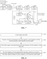
- phase adjusting circuit 40 is also added into the pulse signal generation circuit of the embodiments of the disclosure. Referring to FIG. 7 , the input end of the phase adjusting circuit 40 is connected with the output end of the clock frequency division unit 10, and the output end of the phase adjusting circuit 40 is connected with the input end of the selection unit 30.
- the phase adjusting circuit 40 is configured to adjust the phase of the clock frequency division signal, so as to synchronize the rising edges of the clock frequency division signal and the time delay signal.
- the rising edge of the time delay signal is later than the rising edge of the clock frequency division signal due to the transmission delay time, so the phase adjusting circuit 40 may adjust the phase of the clock frequency division signal backward to synchronize the rising edge of the clock frequency division signal with the rising edge of the time delay signal.
- the phase adjusting circuit 40 may specifically include an inverter and adjusts the phase of the clock signal by using the delay generated by the inverter.
- the selection unit 30 may select the rising edge of the clock frequency division signal or the time delay signal as the rising edge of the pulse signal, and then select the earlier falling edge in the falling edges of the clock frequency division signal and the time delay signal as the falling edge of the pulse signal, to generate the pulse signal. It can also be understood that, the selection unit 30 selects a clock frequency division signal or a time delay signal as a pulse signal to output. Then, the effective level width of the pulse signal may select the effective level width of the clock frequency division signal or the time delay signal according to demands, which avoids the situation that it is difficult to meet the actual demands simply relying on the clock frequency division signal.
- the period of the pulse signal generated by the solution is established based on the period of the clock signal and meets the requirements of a synchronous circuit. On the premise that both the period and the width of the pulse signal meet the demand, the effective level width of the pulse signal is more controllable, so that the memory has good access performance.
- the pulse signal generation circuit of the embodiments may also include a signal driving circuit 50.
- the input end of the signal driving circuit 50 is connected with the output end of the phase adjusting circuit 40, and the output end of the signal driving circuit 50 is connected with the input end of the selection unit 30, so that the selection unit 30 may accurately receive the clock frequency division signal.
- the pulse generation circuit of the embodiments may also include a command input unit 60.
- the command input unit 60 is configured to provide a command signal to the clock frequency division unit 10, so that the clock frequency division unit 10 performs frequency division on the clock signal according to the command signal. Therefore, the output end of the command input unit 60 is connected to the input end of the clock frequency division unit 10.
- the command input unit 60 may be a command receiver, which is configured to receive an external command.
- the pulse generation circuit of the embodiments may also include a command decoding circuit 70. Since the command signal is usually an encoded command, the command decoding circuit 70 is configured to decode the command signal, so that the clock frequency division unit 10 performs frequency division on the clock signal according to the decoded command signal. Therefore, the input end of the command decoding circuit 70 is connected to the output end of the command input unit 60, and the output end of the command decoding circuit 70 is connected to the input end of the clock frequency division unit 10.
- the pulse generation circuit of the embodiments may also include a command latch circuit 80, which is configured to latch a command signal. Therefore, the input end of the command latch circuit 80 is connected to the output end of the command input unit 60, and the output end of the command latch circuit 80 is connected to the input end of the command decoding circuit 70.
- FIG. 8 illustrates a pulse signal generation method according to the embodiments of the disclosure, which includes the following operations.
- frequency division is performed on the clock signal by a clock frequency division unit 10 to generate a clock frequency division signal.
- a time delay signal is generated by a time delay unit 20 based on the clock frequency division signal.
- a setting circuit 21 is utilized to output a setting pulse in response to receiving the rising edge of the clock frequency division signal; a trigger 22 is utilized to output a triggering level in response to receiving the setting pulse; a time delay circuit 23 is utilized to delay the triggering level and output a delayed triggering level; and a reset circuit 24 is utilized to output a reset pulse in response to receiving the rising edge of the delayed triggering level, so as to generate a time delay signal.
- the above method may also include: adjusting the phase of the clock frequency division signal output by the clock frequency division unit 10 by using the phase adjusting circuit 40 to synchronize the rising edges of the clock frequency division signal and the time delay signal.
- the clock frequency division signal and the time delay signal are received by a selection unit 30 at the same time, and selection operation is performed on the clock frequency division signal and the time delay signal according to a preset condition to generate the pulse signal.
- the preset condition may be as follows.
- the clock frequency division signal and the time delay signal are compared, the later rising edge in the rising edges of the clock frequency division signal and the time delay signal is selected as the rising edge of the pulse signal, and the earlier falling edge in the falling edges of the clock frequency division signal and the time delay signal is selected as the falling edge of the pulse signal, so as to generate the pulse signal.
- the selection unit 30 may select the rising edge of the clock frequency division signal or the time delay signal as the rising edge of the pulse signal, and select the earlier falling edge in the falling edges of the clock frequency division signal and the time delay signal as the falling edge of the pulse signal, so as to generate the pulse signal
- the preset condition may also be other conditions, for which details may refer to the abovementioned descriptions and will not be elaborated here.
- the method may also include a plurality of operations, such as inputting a frequency division command signal by the command input unit, or decoding the command signal by the command decoding circuit, or latching the command signal by the command latch circuit, or amplifying the clock frequency division signal by the signal driving circuit, so as to make the generated pulse signal better.
- a plurality of operations such as inputting a frequency division command signal by the command input unit, or decoding the command signal by the command decoding circuit, or latching the command signal by the command latch circuit, or amplifying the clock frequency division signal by the signal driving circuit, so as to make the generated pulse signal better.
- the embodiments of the disclosure further provide a memory, which may include the abovementioned pulse signal generation circuit, and thus it has good access performance.
- the memory may include, but is not limited to, a DRAM, a Synchronous Dynamic Random-Access Memory (SDRAM), a Double Data Rate SDRAM (DDR SDRAM) and other memories.
- SDRAM Synchronous Dynamic Random-Access Memory
- DDR SDRAM Double Data Rate SDRAM
Landscapes
- Physics & Mathematics (AREA)
- Engineering & Computer Science (AREA)
- Computer Hardware Design (AREA)
- Nonlinear Science (AREA)
- Computing Systems (AREA)
- General Engineering & Computer Science (AREA)
- Mathematical Physics (AREA)
- Microelectronics & Electronic Packaging (AREA)
- Pulse Circuits (AREA)
Abstract
Description
- The disclosure claims priority to
Chinese Patent Application No. 202011279041.0, filed on November 16, 2020 - The disclosure relates to the technical field of semiconductors, and in particular to a pulse signal generation circuit and method, and a memory including the pulse signal generation circuit.
- Taking a Dynamic Random-Access Memory (DRAM) as an example, when a memory performs access action, it needs to generate a series of control signals, which are usually pulse signals with a certain width.
- The effective level width of the control pulse signals seriously affects the performance of the memory. If the width is too wide, the access speed of the memory may decrease, and if the width is too narrow, the internal operations of the memory may not be completed. Therefore, it is necessary to reasonably control the effective level width of the pulse signal to ensure a good access performance of the memory. However, for the memory with higher performance requirements and smaller size, the existing pulse signal generation circuits are difficult to meet the demand.
- It is to be noted that information disclosed in the background part is merely used for enhancing understanding of the background of the disclosure, so that information, which does not constitute the conventional art known by those of ordinary skill in the art, may be included.
- The purpose of the disclosure is to overcome the disadvantages of the related art and to provide a pulse signal generation circuit, a pulse signal generation method and a memory.
- According to a first aspect of the disclosure, a pulse signal generation circuit is provided, which includes a clock frequency division unit, a time delay unit and a selection unit.
- An input end of the clock frequency division unit receives a clock signal, and the clock frequency division unit is configured to perform frequency division on the clock signal to generate a clock frequency division signal.
- An input end of the time delay unit is connected to an output end of the clock frequency division unit, and the time delay unit is configured to generate a time delay signal based on the clock frequency division signal.
- Input ends of the selection unit are respectively connected to the output end of the clock frequency division unit and an output end of the time delay unit. The selection unit is configured to receive the clock frequency division signal and the time delay signal at the same time, and perform selection on the clock frequency division signal and the time delay signal according to a preset condition to generate the pulse signal.
- According to a second aspect of the disclosure, a pulse signal generation method is provided, which includes the following operations.
- A clock signal is provided.
- Frequency division on the clock signal is performed by the clock frequency division unit to generate a clock frequency division signal.
- A time delay signal is generated by a time delay unit based on the clock frequency division signal.
- The clock frequency division signal and the time delay signal are received by a selection unit, and selection is performed on the clock frequency division signal and the time delay signal according to a preset condition to generate the pulse signal.
- According to a third aspect of the disclosure, a memory is provided, which includes the pulse signal generation circuit as described above.
- In the disclosure, the effective level width of the pulse signal generated by the pulse signal generation circuit may be controlled based on the time delay time and the multiple of the external clock period at the same time, so as to avoid the situation that the effective level width cannot fully meet the demand simply by relying on the clock signal to generate pulses. Meanwhile, the period of the pulse signal of the disclosure is established based on the period of the clock signal and meets the requirements of a synchronous circuit. On the premise that both the period and the width of the pulse signal meet the demand, the effective level width of the pulse signal of the disclosure is more controllable, so that the memory has good access performance.
- It is to be understood that the above general descriptions and detail descriptions below are merely exemplary and explanatory, which may not limit the disclosure.
- The accompanying drawings here, which are incorporated in and constitute a part of this specification, illustrate embodiments consistent with the disclosure and, together with the description, serve to explain the principles of the disclosure. It is apparent that the drawings described below are only some embodiments of the disclosure. Other drawings may further be obtained by those of ordinary skilled in the art according to these drawings without creative work.
-
FIG. 1 is a schematic structural diagram of a pulse signal generation circuit according to some embodiments of the disclosure. -
FIG. 2 is a schematic structural diagram of a pulse signal generation circuit in an embodiment of the disclosure. -
FIG. 3 is a timing sequence comparison diagram of various signals in the first embodiment of the disclosure. -
FIG. 4 is a timing sequence comparison diagram of various signals in the second embodiment of the disclosure. -
FIG. 5 is a timing sequence comparison diagram of various signals in the third embodiment of the disclosure. -
FIG. 6 is a timing sequence comparison diagram of various signals in the fourth embodiment of the disclosure. -
FIG. 7 is a schematic structural diagram of a pulse signal generation circuit in another embodiment of the disclosure. -
FIG. 8 is a flowchart of a pulse signal generation method according to some embodiments of the disclosure. - Reference numerals in the drawings are as follows. 10. Clock frequency division unit; 20. Time delay unit; 21. Setting circuit; 22. Trigger; 23. Time delay circuit; 24. Reset circuit; 40. Signal driving circuit; 30. Selection unit; 40. Phase adjusting circuit; 50. Signal driving circuit; 60. Command input unit; 70. Command decoding circuit; 80. Command latch circuit.
- Exemplary embodiments will now be described more fully with reference to the drawings. However, the exemplary embodiments may be implemented in many forms, and should not be understood as limitation to embodiments described herein. On the contrary, these provided embodiments enable the disclosure to be more comprehensive and complete, and conceptions of the exemplary embodiments are fully conveyed to those skilled in the art. The same signs in the drawings represent same or similar structures, and thus detailed descriptions thereof are omitted.
- In related art, a suitable pulse signal is the necessary premise to realize the access actions inside a memory. One generation method of a pulse signal is to perform frequency division on a clock signal. The effective level width of the pulse signal obtained by the method is constrained by the period of the clock signal. As process nodes of the memory become smaller and smaller and the storage speed becomes faster and faster, so the constrained effective level width is difficult to meet the actual demand.
- Embodiments of the disclosure provide a pulse signal generation circuit. As shown in
FIG. 1 , the pulse signal generation circuit in the embodiments of the disclosure includes a clockfrequency division unit 10, atime delay unit 20 and aselection unit 30. An input end of the clockfrequency division unit 10 receives a clock signal, and the clockfrequency division unit 10 is configured to perform frequency division on the clock signal to generate a clock frequency division signal. An input end of thetime delay unit 20 is connected with an output end of the clockfrequency division unit 10, and thetime delay unit 20 is configured to generate a time delay signal based on the clock frequency division signal. Input ends of theselection unit 30 are respectively connected with the output end of the clockfrequency division unit 10 and an output end of thetime delay unit 20. Theselection unit 30 is configured to receive the clock frequency division signal and the time delay signal at the same time, and to perform selection operation on the clock frequency division signal and the time delay signal according to a preset condition to generate a pulse signal. - Based on the above circuit structure, the period of the pulse signal is established based on the period of the clock signal, and is consistent with the frequency-divided clock signal. Therefore, the pulse signal meets the requirements of a synchronous circuit. The effective level width of the pulse signal may be selected according to demands, which avoids the situation that it is difficult to meet the actual demands by simply relying on the clock frequency division signal. On the premise that both the period and the width of the pulse signal may meet the demands, the effective level width of the pulse signal of the disclosure is more controllable, so that the memory has good access performance.
- The pulse signal generation circuit according to the embodiments of the disclosure is described in detail below.
- The clock
frequency division unit 10 is configured to reduce the frequency of the clock signal to 1/N of that of the clock signal. Its purpose is to make the periods of the subsequent clock frequency division signal and time delay signal be established based on the period of the clock signal. Therefore, it is not necessary to separately set a circuit for synchronization with the clock signal, which saves the area of the circuit structure. - Herein, if N is even, it is even frequency division, and if N is odd, it is odd frequency division. For example, when N=2, the clock
frequency division unit 10 is a two-frequency-division clock frequency division circuit, and the clockfrequency division unit 10 outputs a periodic signal when a clock triggers two periods every time. Either even frequency division or odd frequency division may be realized by a counter. For example, an even clock frequency division unit may be composed of a counter, an inverter and a trigger, and its working principle is to take input clock signals of a clock source as counting pulses. Because the output end of the counter outputs pulses according to a certain rule, the signal pulses output by different ports may be regarded as the frequency division of the input signal. The working process of frequency division is determined by the selected counter. Thus, if a binary counter is selected, it is a two-frequency-division clock circuit; if an eight-frequency-division counter is selected, it is an eight-frequency-division clock circuit, and so on. Therefore, when the counter is full, it will send an enable signal to thetrigger 22. After receiving the enable signal, the trigger will receive a source clock signal processed by the inverter, and finally, the trigger will output the final frequency division clock. In some circuit systems, there may be a demand for non-integer frequency division on the clock signal, and at this time, a phase-locked loop circuit may be used to realize the non-integer frequency division on the clock. In the embodiment, the clock frequency division signal output from the output end of the clockfrequency division unit 10 is divided into two channels, one is transmitted to theselection unit 30, and the other is transmitted to thetime delay unit 20. - The
time delay unit 20 generates a time delay signal based on the clock frequency division signal, which means that thetime delay unit 20 uses a rising edge of the clock frequency division signal as a rising edge of the time delay signal, delays the rising edge for a certain time, and generates a falling edge, thereby generating the time delay signal. That is, the time delay signal is generated based on the clock frequency division signal, and its period is based on the period of the clock signal. In some technical data, "time delay" is also referred to as "delay". In the disclosure, "time delay" and "delay" mean the same. - In some embodiments, referring to
FIG. 2 , thetime delay unit 20 includes asetting circuit 21, atrigger 22, atime delay circuit 23 and areset circuit 24, which are sequentially connected in series. An input end of the settingcircuit 21 is connected to the output end of the clockfrequency division unit 10, and the settingcircuit 21 is configured to generate a setting pulse in response to receiving the rising edge of the clock frequency division signal from the clockfrequency division unit 10. An input end of thetrigger 22 is connected to the output end of the settingcircuit 21, the output end of thetrigger 22 is the output end of thetime delay unit 20, and thetrigger 22 is configured to output the triggering level in response to receiving the setting pulse generated by the settingcircuit 21. An input end of thetime delay circuit 23 is connected to the output end of thetrigger 22, and thetime delay circuit 23 is configured to delay the triggering level output by thetrigger 22 and output the delayed triggering level. An input end of thereset circuit 24 is connected to the output end of thetime delay circuit 23, the output end of thereset circuit 24 is connected to the input end of thetrigger 22, and thereset circuit 24 is configured to output a reset pulse in response to receiving the rising edge of the delayed triggering level. - In some embodiments, the
trigger 22 adopts a reset/set trigger, that is, RS trigger. The input and output ends of two NOR gates (or NAND gates) are in cross connection to form a basic RS trigger. As shown inFIG. 2 , it is an RS trigger having reset and set functions and composed of two NOR gates in cross coupling. Its input end S is connected to the output end of the settingcircuit 21, the input end R is connected to the output end of thereset circuit 24, and the output end Q is the output end of the NOR gate connected to the input end R. - The setting
circuit 21 outputs a setting pulse upon receiving the rising edge of the clock frequency division signal. At this time, the output end Q of the RS trigger outputs 1, that is, a rising edge of a triggering level is generated. The rising edge is delayed by thetime delay circuit 23 for a period of time to form a high-level signal with a certain width, and then output the same to the reset circuit. Thereset circuit 24 outputs a reset pulse upon receiving the rising edge of the triggering level delayed by thetime delay circuit 23. At this time, the output end Q of the RS trigger outputs 0, that is, a falling edge of the triggering level is generated. The falling edge is delayed by thetime delay circuit 23 for a period of time to form a low-level signal with a certain width. When the settingcircuit 21 receives the rising edge of the clock frequency division signal again, it outputs 1 again, and the process cycles, thereby to form a square wave pulse signal with a certain effective level width, that is, a time delay signal. - The
time delay circuit 23 may be realized by any circuit structure that may realize the time delay function., for example, an even number of connected inverters may be adopted and some capacitors may also be included, or thetime delay circuit 23 may also be realized by a buffer(s), which is not specially limited in the disclosure. The effective level width of the time delay signal is determined by time delay parameters of thetime delay circuit 23, and the time delay parameters may be adjusted as needed. In some embodiments, thetime delay circuit 23 is a fixed time delay circuit, which means that the time of each delay is equal, and thus it is a fixed time delay. In other embodiments, thetime delay circuit 23 may also be a variable time delay circuit, that is, the time of each delay may be different. The settingcircuit 21 and thereset circuit 24 may adopt the same circuit structure, or they may also be different circuit structures. - In some embodiments, the preset condition for the selection unit to select the clock frequency division signal and the time delay signal is as follows. The later rising edge in the rising edges of the clock frequency division signal and the time delay signal is selected as the rising edge of the pulse signal, and the earlier falling edge in the falling edges of the clock frequency division signal and the time delay signal is selected as the falling edge of the pulse signal, so as to generate a pulse signal. Therefore, the
selection unit 30 may include an AND gate, the first input end of which is connected to the output end of the clockfrequency division unit 10, and the second input end of which is connected to the output end of thetrigger 22. Only when the clock frequency division signal and the time delay signal are at high level, the AND gate will output a high level, otherwise it will output a low level. - The mode of generating a pulse signal by the above circuit structure is described in detail below in combination with the timing sequence diagrams.
- For example,
FIG. 3 illustrates timing sequence diagrams of a clock signal, a clock frequency division signal, a time delay signal and a pulse signal. Herein, the clockfrequency division unit 10 performs eight frequency divisions on the clock signal, so that the period of the clock frequency division signal and the period of the time delay signal are eight times of the period of the clock signal, and the time delay circuit is a fixed time delay circuit. In some embodiments, the rising edges of the clock frequency division signal and the time delay signal are synchronized. At this time, the AND gate synchronously receives the rising edges of the clock frequency division signal and the time delay signal and outputs a high level. The effective level width of the clock frequency division signal is less than the effective level width of the time delay signal, and thus the falling edge of the clock frequency division signal arrives earlier than the falling edge of the time delay signal. At this time, the AND gate outputs a low level upon receiving the falling edge of the clock frequency division signal. Therefore, the effective level width of the pulse signal output by the AND gate is equal to that of the clock frequency division signal. - For another example, referring to
FIG. 4 , unlikeFIG. 3 , the effective level width of the clock frequency division signal is greater than that of the time delay signal. The rising edges of the clock frequency division signal and the time delay signal are synchronized. At this time, the AND gate synchronously receives the rising edges of the clock frequency division signal and the time delay signal and outputs a high level. The effective level width of the clock frequency division signal is greater than the effective level width of the time delay signal, and thus the falling edge of the time delay signal arrives earlier than the falling edge of the clock frequency division signal. At this time, the AND gate outputs a low level upon receiving the falling edge of the time delay signal. Therefore, the effective level width of the pulse signal output by the AND gate is equal to that of the time delay signal. - In the examples shown in
FIG. 3 and FIG. 4 , the rising edges of the clock frequency division signal and the time delay signal are synchronized, which may ensure that the pulse signal may be easily modulated by the clock signal. However, for some practical circuits, considering the factors such as process, and circuit characteristics, there will be a period of time from the time when the clock frequency division signal reaches the settingcircuit 21 to the time when the new state at the output end of thetrigger 22 is stably established. The elapsed time is the transmission delay time of thetrigger 22. When the transmission delay time is relatively large, the rising edge of the time delay signal is not synchronized with the rising edge of the clock frequency division signal, and is later than the rising edge of the clock frequency division signal. - For example, referring to
FIG. 5 , the rising edge of the clock frequency division signal arrives earlier than the rising edge of the time delay signal, and the AND gate outputs a high level only when receiving the rising edge of the time delay signal. The falling edge of the clock frequency division signal also arrives earlier than the falling edge of the time delay signal, and the AND gate outputs a low level upon receiving the falling edge of the clock frequency division signal. As a result, the effective level width of the pulse signal output by the AND gate is the width from the rising edge of the time delay signal to the falling edge of the clock frequency division signal. - For another example, referring to
FIG. 6 , the rising edge of the clock frequency division signal arrives earlier than the rising edge of the time delay signal, and the AND gate outputs a high level only when receiving the rising edge of the time delay signal. The falling edge of the time delay signal arrives earlier than the falling edge of the clock frequency division signal, and the AND gate outputs a low level upon receiving the falling edge of the time delay signal. Therefore, the effective level width of the pulse signal output by the AND gate is the width from the rising edge of the time delay signal to the falling edge of the time delay signal, that is, the effective level width of the pulse signal output by the AND gate is equal to the effective level width of the time delay signal. - The embodiments of
FIG. 3 to FIG. 6 show different selection processes under a preset condition. In other embodiments, the preset condition may also be other conditions, for example, the earlier rising edge in the rising edges of the clock frequency division signal and the time delay signal is selected as the rising edge of the pulse signal, and the later falling edge in the falling edges of the clock frequency division signal and the time delay signal is selected as the falling edge of the pulse signal to generate the pulse signal. In short, the preset condition may be set according to the requirements of the memory for the effective level width of the pulse signal, so that the selection unit may select suitable rising edge and falling edge. - Continuing with the examples of
FIG. 5 and FIG. 6 , since the rising edges of the clock frequency division signal and the time delay signal are not synchronized, the pulse signal output from the AND gate will not be synchronized with the clock signal, thereby affecting the access performance. Therefore, the ideal way is to synchronize the rising edges of the clock frequency division signal and the time delay signal. In order to avoid the problem, aphase adjusting circuit 40 is also added into the pulse signal generation circuit of the embodiments of the disclosure. Referring toFIG. 7 , the input end of thephase adjusting circuit 40 is connected with the output end of the clockfrequency division unit 10, and the output end of thephase adjusting circuit 40 is connected with the input end of theselection unit 30. Thephase adjusting circuit 40 is configured to adjust the phase of the clock frequency division signal, so as to synchronize the rising edges of the clock frequency division signal and the time delay signal. The rising edge of the time delay signal is later than the rising edge of the clock frequency division signal due to the transmission delay time, so thephase adjusting circuit 40 may adjust the phase of the clock frequency division signal backward to synchronize the rising edge of the clock frequency division signal with the rising edge of the time delay signal. Thephase adjusting circuit 40 may specifically include an inverter and adjusts the phase of the clock signal by using the delay generated by the inverter. - After adjustment, the
selection unit 30 may select the rising edge of the clock frequency division signal or the time delay signal as the rising edge of the pulse signal, and then select the earlier falling edge in the falling edges of the clock frequency division signal and the time delay signal as the falling edge of the pulse signal, to generate the pulse signal. It can also be understood that, theselection unit 30 selects a clock frequency division signal or a time delay signal as a pulse signal to output. Then, the effective level width of the pulse signal may select the effective level width of the clock frequency division signal or the time delay signal according to demands, which avoids the situation that it is difficult to meet the actual demands simply relying on the clock frequency division signal. The period of the pulse signal generated by the solution is established based on the period of the clock signal and meets the requirements of a synchronous circuit. On the premise that both the period and the width of the pulse signal meet the demand, the effective level width of the pulse signal is more controllable, so that the memory has good access performance. - In the above embodiments, eight frequency division is taken as an example and the fixed time delay is described. It can be understood by those skilled in the art that, when the clock
frequency division unit 10 performs frequency division by other multiples and the time delay circuit adopts the variable time delay circuit, the generation of the pulse signal may also be achieved through the same idea. - Further, referring to
FIG. 7 , the pulse signal generation circuit of the embodiments may also include asignal driving circuit 50. The input end of thesignal driving circuit 50 is connected with the output end of thephase adjusting circuit 40, and the output end of thesignal driving circuit 50 is connected with the input end of theselection unit 30, so that theselection unit 30 may accurately receive the clock frequency division signal. - Further, referring to
FIG. 7 , the pulse generation circuit of the embodiments may also include acommand input unit 60. Thecommand input unit 60 is configured to provide a command signal to the clockfrequency division unit 10, so that the clockfrequency division unit 10 performs frequency division on the clock signal according to the command signal. Therefore, the output end of thecommand input unit 60 is connected to the input end of the clockfrequency division unit 10. Thecommand input unit 60 may be a command receiver, which is configured to receive an external command. - Further, referring to
FIG. 7 , the pulse generation circuit of the embodiments may also include acommand decoding circuit 70. Since the command signal is usually an encoded command, thecommand decoding circuit 70 is configured to decode the command signal, so that the clockfrequency division unit 10 performs frequency division on the clock signal according to the decoded command signal. Therefore, the input end of thecommand decoding circuit 70 is connected to the output end of thecommand input unit 60, and the output end of thecommand decoding circuit 70 is connected to the input end of the clockfrequency division unit 10. - Further, referring to
FIG. 7 , the pulse generation circuit of the embodiments may also include acommand latch circuit 80, which is configured to latch a command signal. Therefore, the input end of thecommand latch circuit 80 is connected to the output end of thecommand input unit 60, and the output end of thecommand latch circuit 80 is connected to the input end of thecommand decoding circuit 70. - In combination with the above circuit structure,
FIG. 8 illustrates a pulse signal generation method according to the embodiments of the disclosure, which includes the following operations. - At
S 100, a clock signal is provided. - At S200, frequency division is performed on the clock signal by a clock
frequency division unit 10 to generate a clock frequency division signal. - At S300, a time delay signal is generated by a
time delay unit 20 based on the clock frequency division signal. - In the operations, the circuit structure shown in
FIG. 2 may be adopted, and the corresponding method includes the following operations. A settingcircuit 21 is utilized to output a setting pulse in response to receiving the rising edge of the clock frequency division signal; atrigger 22 is utilized to output a triggering level in response to receiving the setting pulse; atime delay circuit 23 is utilized to delay the triggering level and output a delayed triggering level; and areset circuit 24 is utilized to output a reset pulse in response to receiving the rising edge of the delayed triggering level, so as to generate a time delay signal. In order to synchronize the rising edges of the clock frequency division signal and the time delay signal, the above method may also include: adjusting the phase of the clock frequency division signal output by the clockfrequency division unit 10 by using thephase adjusting circuit 40 to synchronize the rising edges of the clock frequency division signal and the time delay signal. - At S400, the clock frequency division signal and the time delay signal are received by a
selection unit 30 at the same time, and selection operation is performed on the clock frequency division signal and the time delay signal according to a preset condition to generate the pulse signal. - As mentioned above, the preset condition may be as follows. The clock frequency division signal and the time delay signal are compared, the later rising edge in the rising edges of the clock frequency division signal and the time delay signal is selected as the rising edge of the pulse signal, and the earlier falling edge in the falling edges of the clock frequency division signal and the time delay signal is selected as the falling edge of the pulse signal, so as to generate the pulse signal. For example, when the rising edges of the clock frequency division signal and the time delay signal are synchronized, the
selection unit 30 may select the rising edge of the clock frequency division signal or the time delay signal as the rising edge of the pulse signal, and select the earlier falling edge in the falling edges of the clock frequency division signal and the time delay signal as the falling edge of the pulse signal, so as to generate the pulse signal The preset condition may also be other conditions, for which details may refer to the abovementioned descriptions and will not be elaborated here. - Besides the above operations, the method may also include a plurality of operations, such as inputting a frequency division command signal by the command input unit, or decoding the command signal by the command decoding circuit, or latching the command signal by the command latch circuit, or amplifying the clock frequency division signal by the signal driving circuit, so as to make the generated pulse signal better.
- The embodiments of the disclosure further provide a memory, which may include the abovementioned pulse signal generation circuit, and thus it has good access performance. The memory may include, but is not limited to, a DRAM, a Synchronous Dynamic Random-Access Memory (SDRAM), a Double Data Rate SDRAM (DDR SDRAM) and other memories.
- In the disclosure, terms "one", "a/an", "the", "said", "described" and "at least one" are used to indicate one or more elements/constituent parts/etc. Terms "include" and "have" are used to express an open sense of inclusion and to indicate that additional elements/constituents/ and the like may exist in addition to the listed elements/constituents/ and the like.
- Other implementation solutions of the disclosure will be apparent to those skilled in the art from consideration of the specification and practice of the disclosure disclosed herein. The disclosure is intended to contain any modification, purpose or adaptive change of the disclosure, and they follow general principles of the disclosure and include common general knowledge or conventional technical means in the technical field, which is not disclosed by the disclosure. The specification and the embodiments are considered exemplary only, and the true scope and spirit of the disclosure are indicated by the appended claims.
Claims (17)
- A pulse signal generation circuit, comprising:a clock frequency division unit, wherein an input end of the clock frequency division unit receives a clock signal, and the clock frequency division unit is configured to perform frequency division on the clock signal to generate a clock frequency division signal;a time delay unit, wherein an input end of the time delay unit is connected to an output end of the clock frequency division unit, and the time delay unit is configured to generate a time delay signal based on the clock frequency division signal; anda selection unit, wherein input ends of the selection unit are respectively connected to the output end of the clock frequency division unit and an output end of the time delay unit, and the selection unit is configured to receive the clock frequency division signal and the time delay signal at the same time, and perform selection on the clock frequency division signal and the time delay signal according to a preset condition to generate a pulse signal.
- The pulse signal generation circuit according to claim 1, wherein the preset condition is as follows: selecting a later rising edge in a rising edge of the clock frequency division signal and a rising edge of the time delay signal as a rising edge of the pulse signal, and selecting an earlier falling edge in a falling edge of the clock frequency division signal and a falling edge of the time delay signal as a falling edge of the pulse signal.
- The pulse signal generation circuit according to claim 2, wherein the time delay unit comprises:a setting circuit, wherein an input end of the setting circuit is connected to the output end of the clock frequency division unit, and the setting circuit is configured to output a setting pulse in response to receiving the rising edge of the clock frequency division signal;a trigger, wherein an input end of the trigger is connected to an output end of the setting circuit, and an output end of the trigger is the output end of the time delay unit, and wherein the trigger is configured to output a triggering level in response to receiving the setting pulse;a time delay circuit, wherein an input end of the time delay circuit is connected to the output end of the trigger, and the time delay circuit is configured to delay the triggering level and output a delayed triggering level; anda reset circuit, wherein an input end of the reset circuit is connected to an output end of the time delay circuit, and an output end of the reset circuit is connected to the input end of the trigger, and wherein the reset circuit is configured to output a reset pulse in response to receiving a rising edge of the delayed triggering level.
- The pulse signal generation circuit according to claim 3, wherein the time delay circuit is a fixed time delay circuit.
- The pulse signal generation circuit according to claim 3, wherein the trigger is a reset/set (RS) trigger.
- The pulse signal generation circuit according to claim 3, wherein the selection unit comprises an AND gate, wherein a first input end of the AND gate is connected to the output end of the clock frequency division unit, and a second input end of the AND gate is connected to the output end of the trigger.
- The pulse signal generation circuit according to claim 1, wherein the clock frequency division unit is frequency divided by an even number.
- The pulse signal generation circuit according to claim 1, further comprising:a phase adjusting circuit, wherein an input end of the phase adjusting circuit is connected to the output end of the clock frequency division unit, and an output end of the phase adjusting circuit is connected to the input end of the selection unit, and wherein the phase adjusting circuit is configured to adjust a phase of the clock frequency division signal to synchronize a rising edge of the clock frequency division signal and a rising edge of the time delay signal;wherein the selection unit is further configured to: select the rising edge of the clock frequency division signal or the rising edge of the time delay signal as a rising edge of the pulse signal, and select an earlier falling edge in a falling edge of the clock frequency division signal and a falling edge of the time delay signal as a falling edge of the pulse signal, to generate the pulse signal.
- The pulse signal generation circuit according to claim 8, further comprising:
a signal driving circuit, wherein an input end of the signal driving circuit is connected to the output end of the phase adjusting circuit, and an output end of the signal driving circuit is connected to the input end of the selection unit. - The pulse signal generation circuit according to claim 1, further comprising:
a command input unit, wherein an output end of the command input unit is connected to the input end of the clock frequency division unit, and the command input unit is configured to provide a command signal to the clock frequency division unit so that the clock frequency division unit performs frequency division on the clock signal according to the command signal. - The pulse signal generation circuit according to claim 10, further comprising:
a command decoding circuit, wherein an input end of the command decoding circuit is connected to the output end of the command input unit, and an output end of the command decoding circuit is connected to the input end of the clock frequency division unit, and wherein the command decoding circuit is configured to decode the command signal to obtain a decoded command signal so that the clock frequency division unit performs frequency division on the clock signal according to the decoded command signal. - The pulse signal generation circuit according to claim 11, further comprising:
a command latch circuit, wherein an input end of the command latch circuit is connected to the output end of the command input unit, and an output end of the command latch circuit is connected to the input end of the command decoding circuit, and wherein the command latch circuit is configured to latch the command signal. - A pulse signal generation method, comprising:providing a clock signal;performing frequency division on the clock signal by a clock frequency division unit to generate a clock frequency division signal;generating a time delay signal by a time delay unit based on the clock frequency division signal; andreceiving the clock frequency division signal and the time delay signal by a selection unit at the same time, and performing selection on the clock frequency division signal and the time delay signal according to a preset condition to generate a pulse signal.
- The pulse signal generation method according to claim 13, wherein the preset condition is as follows: selecting a later rising edge in a rising edge of the clock frequency division signal and a rising edge of the time delay signal as a rising edge of the pulse signal, and selecting an earlier falling edge in a falling edge of the clock frequency division signal and a falling edge of the time delay signal as a falling edge of the pulse signal.
- The pulse signal generation method according to claim 14, wherein delaying the clock frequency division signal by a time delay circuit to generate a time delay signal comprises:outputting a setting pulse by a setting circuit in response to receiving the rising edge of the clock frequency division signal;outputting a triggering level by a trigger in response to receiving the setting pulse;delaying the triggering level by a time delay circuit and outputting a delayed triggering level; andoutputting a reset pulse by a reset circuit in response to receiving a rising edge of the delayed triggering level, thereby generating the time delay signal.
- The pulse signal generation method according to claim 13, further comprising:adjusting a phase of the clock frequency division signal by a phase adjusting circuit to synchronize a rising edge of the clock frequency division signal and a rising edge of the time delay signal,wherein the selection unit selects a rising edge of the clock frequency division signal or a rising edge of the time delay signal as a rising edge of the pulse signal, and selects an earlier falling edge in a falling edge of the clock frequency division signal and a falling edge of the time delay signal as a falling edge of the pulse signal, to generate the pulse signal.
- A memory, comprising the pulse signal generation circuit according to any one of claims 1-12.
Applications Claiming Priority (2)
| Application Number | Priority Date | Filing Date | Title |
|---|---|---|---|
| CN202011279041.0A CN114513199B (en) | 2020-11-16 | 2020-11-16 | Pulse signal generating circuit and generating method, and memory |
| PCT/CN2021/108544 WO2022100149A1 (en) | 2020-11-16 | 2021-07-27 | Pulse signal generation circuit and generation method, and memory |
Publications (2)
| Publication Number | Publication Date |
|---|---|
| EP4203313A1 true EP4203313A1 (en) | 2023-06-28 |
| EP4203313A4 EP4203313A4 (en) | 2024-03-20 |
Family
ID=81586911
Family Applications (1)
| Application Number | Title | Priority Date | Filing Date |
|---|---|---|---|
| EP21890680.8A Pending EP4203313A4 (en) | 2020-11-16 | 2021-07-27 | PULSE SIGNAL GENERATION CIRCUIT AND METHOD AND MEMORY |
Country Status (2)
| Country | Link |
|---|---|
| US (1) | US11671106B2 (en) |
| EP (1) | EP4203313A4 (en) |
Families Citing this family (1)
| Publication number | Priority date | Publication date | Assignee | Title |
|---|---|---|---|---|
| EP4203313A4 (en) * | 2020-11-16 | 2024-03-20 | Changxin Memory Technologies, Inc. | PULSE SIGNAL GENERATION CIRCUIT AND METHOD AND MEMORY |
Family Cites Families (33)
| Publication number | Priority date | Publication date | Assignee | Title |
|---|---|---|---|---|
| KR100512935B1 (en) * | 2002-05-24 | 2005-09-07 | 삼성전자주식회사 | Internal clock signal generating circuit and method |
| US6680874B1 (en) | 2002-08-29 | 2004-01-20 | Micron Technology, Inc. | Delay lock loop circuit useful in a synchronous system and associated methods |
| US7259604B2 (en) * | 2005-08-03 | 2007-08-21 | Micron Technology, Inc. | Initialization scheme for a reduced-frequency, fifty percent duty cycle corrector |
| JPWO2009031191A1 (en) * | 2007-09-03 | 2010-12-09 | 富士通株式会社 | Clock output circuit |
| US20090086511A1 (en) * | 2007-09-27 | 2009-04-02 | Phison Electronics Corp. | Converter circuit with pulse width frequency modulation and method thereof |
| JP5262630B2 (en) * | 2008-12-01 | 2013-08-14 | 富士通株式会社 | Clock generation circuit having self-test circuit |
| US8299826B2 (en) * | 2009-08-25 | 2012-10-30 | Sitime Corporation | Phase locked loop circuitry having switched resistor loop filter circuitry, and methods of operating same |
| CN201804106U (en) | 2010-08-25 | 2011-04-20 | 天津七六四通信导航技术有限公司 | Novel answer probability tester |
| US8861303B2 (en) * | 2012-04-26 | 2014-10-14 | Macronix International Co., Ltd. | Circuit and method for address transition detection |
| KR102107076B1 (en) * | 2013-12-02 | 2020-05-08 | 에스케이하이닉스 주식회사 | Semiconductor apparatus |
| US9397668B2 (en) * | 2014-12-18 | 2016-07-19 | Linear Technology Corporation | System and method for providing programmable synchronous output delay in a clock generation or distribution device |
| US9768760B2 (en) * | 2015-03-11 | 2017-09-19 | Micron Technology, Inc. | Synchronized semiconductor device with phase adjustment circuit |
| CN206164491U (en) | 2016-10-12 | 2017-05-10 | 成都卓创科微电子有限公司 | Take wide region delay circuit of mode switch function |
| US9973178B1 (en) * | 2017-02-16 | 2018-05-15 | Nuvoton Technology Corporation | Method and apparatus for clock frequency multiplier |
| CN108736894B (en) * | 2017-04-18 | 2021-08-06 | 博通集成电路(上海)股份有限公司 | fractional-N frequency synthesizer and method therefor |
| KR102268767B1 (en) * | 2017-06-09 | 2021-06-29 | 에스케이하이닉스 주식회사 | Delay circuit and duty cycle controller including the same |
| US10156603B1 (en) * | 2017-06-14 | 2018-12-18 | University Of Electronic Science And Technology Of China | Apparatus for adding jitters to the edges of a pulse sequence |
| US10996634B2 (en) * | 2018-01-05 | 2021-05-04 | Samsung Electronics Co., Ltd. | System and method for fast-converging digital-to-time converter (DTC) gain calibration for DTC-based analog fractional-N phase lock loop (PLL) |
| KR102528561B1 (en) * | 2018-05-09 | 2023-05-04 | 삼성전자주식회사 | Apparatus and method for generating clock |
| US10778236B2 (en) * | 2019-01-04 | 2020-09-15 | Credo Technology Group Limited | PLL with wide frequency coverage |
| US11126216B2 (en) * | 2019-01-15 | 2021-09-21 | SK Hynix Inc. | Signal generation circuit synchronized with a clock signal and a semiconductor apparatus using the same |
| JP7324013B2 (en) * | 2019-02-15 | 2023-08-09 | キヤノン株式会社 | Fractional divider and frequency synthesizer |
| JP7314685B2 (en) * | 2019-07-25 | 2023-07-26 | セイコーエプソン株式会社 | Timepieces, electronic devices and moving bodies |
| US11049543B2 (en) * | 2019-09-03 | 2021-06-29 | Micron Technology, Inc. | Apparatuses and methods for deactivating a delay locked loop update in semiconductor devices |
| US11750201B2 (en) * | 2019-09-06 | 2023-09-05 | SK Hynix Inc. | Delay line, a delay locked loop circuit and a semiconductor apparatus using the delay line and the delay locked loop circuit |
| CN111049504A (en) | 2019-11-22 | 2020-04-21 | 深圳市德赛微电子技术有限公司 | Pulse generating circuit |
| KR102847326B1 (en) * | 2019-12-10 | 2025-08-14 | 삼성전자주식회사 | Clock data recovery circuit, apparatus including the same |
| US10944407B1 (en) * | 2020-06-03 | 2021-03-09 | Stmicroelectronics International N.V. | Source synchronous interface with selectable delay on source and delay on destination control |
| KR102816578B1 (en) * | 2020-08-14 | 2025-06-04 | 삼성전자주식회사 | Duty adjustment circuit, and delay locked loop circuit and semiconductor memory device having the same |
| EP4203313A4 (en) * | 2020-11-16 | 2024-03-20 | Changxin Memory Technologies, Inc. | PULSE SIGNAL GENERATION CIRCUIT AND METHOD AND MEMORY |
| US11870446B2 (en) * | 2021-01-12 | 2024-01-09 | Texas Instruments Incorporated | High gain detector techniques for low bandwidth low noise phase-locked loops |
| US11277140B1 (en) * | 2021-06-07 | 2022-03-15 | Qualcomm Incorporated | Sampling phase-locked loop |
| EP4125212A1 (en) * | 2021-07-27 | 2023-02-01 | NXP USA, Inc. | Pulse stretching circuit |
-
2021
- 2021-07-27 EP EP21890680.8A patent/EP4203313A4/en active Pending
-
2022
- 2022-01-27 US US17/649,181 patent/US11671106B2/en active Active
Also Published As
| Publication number | Publication date |
|---|---|
| US20220158645A1 (en) | 2022-05-19 |
| US11671106B2 (en) | 2023-06-06 |
| EP4203313A4 (en) | 2024-03-20 |
Similar Documents
| Publication | Publication Date | Title |
|---|---|---|
| CN114513199B (en) | Pulse signal generating circuit and generating method, and memory | |
| EP3449377B1 (en) | Methods and apparatuses including command delay adjustment circuit | |
| US10886927B2 (en) | Signal generation circuit synchronized with a clock signal and a semiconductor apparatus using the same | |
| US7826583B2 (en) | Clock data recovery apparatus | |
| KR101046227B1 (en) | DLD circuit | |
| KR100540487B1 (en) | Data output control circuit | |
| US9543968B2 (en) | Output control circuit for semiconductor apparatus and output driving circuit including the same | |
| US7233533B2 (en) | Method for controlling data output timing of memory device and device therefor | |
| US6150859A (en) | Digital delay-locked loop | |
| US7737744B2 (en) | Register controlled delay locked loop circuit | |
| US7535274B2 (en) | Delay control circuit | |
| US11671106B2 (en) | Pulse signal generation circuit and method, and memory | |
| KR100525096B1 (en) | DLL circuit | |
| US6894539B2 (en) | Delay locked loop having phase comparator | |
| CN116192126A (en) | A delay-locked loop and memory | |
| CN101110582B (en) | delay control circuit | |
| US8295121B2 (en) | Clock buffer and a semiconductor memory apparatus using the same | |
| CN105261382A (en) | Output circuit | |
| KR102841010B1 (en) | Memory apparatus, a semiconductor system including the same and an operating method thereof | |
| KR20240029185A (en) | Clock generating circuit and a semiconductor apparatus using the clock generating circuit | |
| US20250015786A1 (en) | Clock doubler, a clock generating device and a semiconductor system using the same | |
| CN117806417A (en) | Training circuit and training method suitable for write equalization | |
| CN111382093A (en) | Source synchronous circuit of data transmission interface | |
| CN109600129B (en) | Delay unit and delay line circuit | |
| KR100336759B1 (en) | Clock signal selection circuit |
Legal Events
| Date | Code | Title | Description |
|---|---|---|---|
| STAA | Information on the status of an ep patent application or granted ep patent |
Free format text: STATUS: THE INTERNATIONAL PUBLICATION HAS BEEN MADE |
|
| PUAI | Public reference made under article 153(3) epc to a published international application that has entered the european phase |
Free format text: ORIGINAL CODE: 0009012 |
|
| STAA | Information on the status of an ep patent application or granted ep patent |
Free format text: STATUS: REQUEST FOR EXAMINATION WAS MADE |
|
| 17P | Request for examination filed |
Effective date: 20230321 |
|
| AK | Designated contracting states |
Kind code of ref document: A1 Designated state(s): AL AT BE BG CH CY CZ DE DK EE ES FI FR GB GR HR HU IE IS IT LI LT LU LV MC MK MT NL NO PL PT RO RS SE SI SK SM TR |
|
| DAV | Request for validation of the european patent (deleted) | ||
| DAX | Request for extension of the european patent (deleted) | ||
| A4 | Supplementary search report drawn up and despatched |
Effective date: 20240220 |
|
| RIC1 | Information provided on ipc code assigned before grant |
Ipc: G11C 11/4076 20060101ALI20240214BHEP Ipc: G11C 7/22 20060101ALI20240214BHEP Ipc: H03K 5/135 20060101ALI20240214BHEP Ipc: H03K 5/05 20060101ALI20240214BHEP Ipc: G11C 11/4063 20060101ALI20240214BHEP Ipc: H03K 5/06 20060101ALI20240214BHEP Ipc: H03K 7/08 20060101AFI20240214BHEP |
|
| GRAP | Despatch of communication of intention to grant a patent |
Free format text: ORIGINAL CODE: EPIDOSNIGR1 |
|
| STAA | Information on the status of an ep patent application or granted ep patent |
Free format text: STATUS: GRANT OF PATENT IS INTENDED |
|
| INTG | Intention to grant announced |
Effective date: 20251222 |
|
| P01 | Opt-out of the competence of the unified patent court (upc) registered |
Free format text: CASE NUMBER: UPC_APP_0000003_4203313/2026 Effective date: 20260102 |
|
| GRAS | Grant fee paid |
Free format text: ORIGINAL CODE: EPIDOSNIGR3 |
|
| GRAA | (expected) grant |
Free format text: ORIGINAL CODE: 0009210 |
|
| STAA | Information on the status of an ep patent application or granted ep patent |
Free format text: STATUS: THE PATENT HAS BEEN GRANTED |