EP4198499A1 - Surface-enhanced raman scattering unit - Google Patents
Surface-enhanced raman scattering unit Download PDFInfo
- Publication number
- EP4198499A1 EP4198499A1 EP23156265.3A EP23156265A EP4198499A1 EP 4198499 A1 EP4198499 A1 EP 4198499A1 EP 23156265 A EP23156265 A EP 23156265A EP 4198499 A1 EP4198499 A1 EP 4198499A1
- Authority
- EP
- European Patent Office
- Prior art keywords
- raman scattering
- enhanced raman
- sers
- board
- holding
- Prior art date
- Legal status (The legal status is an assumption and is not a legal conclusion. Google has not performed a legal analysis and makes no representation as to the accuracy of the status listed.)
- Withdrawn
Links
- 238000004416 surface enhanced Raman spectroscopy Methods 0.000 title claims abstract description 261
- 230000003287 optical effect Effects 0.000 claims abstract description 63
- 239000004020 conductor Substances 0.000 claims description 14
- 239000000758 substrate Substances 0.000 abstract description 40
- 238000005259 measurement Methods 0.000 abstract description 10
- 238000001069 Raman spectroscopy Methods 0.000 description 25
- 239000010410 layer Substances 0.000 description 20
- 238000000034 method Methods 0.000 description 18
- 238000004611 spectroscopical analysis Methods 0.000 description 18
- 230000002542 deteriorative effect Effects 0.000 description 15
- 239000011347 resin Substances 0.000 description 14
- 229920005989 resin Polymers 0.000 description 14
- 239000000853 adhesive Substances 0.000 description 11
- 230000001070 adhesive effect Effects 0.000 description 11
- 239000011521 glass Substances 0.000 description 10
- -1 polypropylene Polymers 0.000 description 9
- 230000005284 excitation Effects 0.000 description 7
- 239000004615 ingredient Substances 0.000 description 7
- LFQSCWFLJHTTHZ-UHFFFAOYSA-N Ethanol Chemical compound CCO LFQSCWFLJHTTHZ-UHFFFAOYSA-N 0.000 description 6
- 239000000463 material Substances 0.000 description 6
- 239000000919 ceramic Substances 0.000 description 5
- 238000000465 moulding Methods 0.000 description 5
- 229920003229 poly(methyl methacrylate) Polymers 0.000 description 4
- 229920000139 polyethylene terephthalate Polymers 0.000 description 4
- 229920001296 polysiloxane Polymers 0.000 description 4
- 239000000843 powder Substances 0.000 description 4
- 229910052710 silicon Inorganic materials 0.000 description 4
- 239000010703 silicon Substances 0.000 description 4
- 229920000106 Liquid crystal polymer Polymers 0.000 description 3
- 239000004977 Liquid-crystal polymers (LCPs) Substances 0.000 description 3
- 239000004698 Polyethylene Substances 0.000 description 3
- 239000004743 Polypropylene Substances 0.000 description 3
- PPBRXRYQALVLMV-UHFFFAOYSA-N Styrene Chemical compound C=CC1=CC=CC=C1 PPBRXRYQALVLMV-UHFFFAOYSA-N 0.000 description 3
- 229920000122 acrylonitrile butadiene styrene Polymers 0.000 description 3
- 238000005520 cutting process Methods 0.000 description 3
- 238000010586 diagram Methods 0.000 description 3
- 239000006185 dispersion Substances 0.000 description 3
- 230000000694 effects Effects 0.000 description 3
- 238000005530 etching Methods 0.000 description 3
- 230000001678 irradiating effect Effects 0.000 description 3
- 238000002844 melting Methods 0.000 description 3
- 229910052751 metal Inorganic materials 0.000 description 3
- 239000002184 metal Substances 0.000 description 3
- 229920000573 polyethylene Polymers 0.000 description 3
- 239000005020 polyethylene terephthalate Substances 0.000 description 3
- 239000004926 polymethyl methacrylate Substances 0.000 description 3
- 229920001155 polypropylene Polymers 0.000 description 3
- 230000000452 restraining effect Effects 0.000 description 3
- XLYOFNOQVPJJNP-UHFFFAOYSA-N water Substances O XLYOFNOQVPJJNP-UHFFFAOYSA-N 0.000 description 3
- 238000001914 filtration Methods 0.000 description 2
- 230000000737 periodic effect Effects 0.000 description 2
- 239000004593 Epoxy Substances 0.000 description 1
- JOYRKODLDBILNP-UHFFFAOYSA-N Ethyl urethane Chemical compound CCOC(N)=O JOYRKODLDBILNP-UHFFFAOYSA-N 0.000 description 1
- PXGOKWXKJXAPGV-UHFFFAOYSA-N Fluorine Chemical compound FF PXGOKWXKJXAPGV-UHFFFAOYSA-N 0.000 description 1
- 229920006397 acrylic thermoplastic Polymers 0.000 description 1
- 229910052782 aluminium Inorganic materials 0.000 description 1
- 229910052804 chromium Inorganic materials 0.000 description 1
- 230000000295 complement effect Effects 0.000 description 1
- 239000000470 constituent Substances 0.000 description 1
- 229910052802 copper Inorganic materials 0.000 description 1
- 238000000151 deposition Methods 0.000 description 1
- 230000006866 deterioration Effects 0.000 description 1
- 238000001704 evaporation Methods 0.000 description 1
- 230000008020 evaporation Effects 0.000 description 1
- 238000010304 firing Methods 0.000 description 1
- 229910052731 fluorine Inorganic materials 0.000 description 1
- 239000011737 fluorine Substances 0.000 description 1
- 229910052737 gold Inorganic materials 0.000 description 1
- 150000002739 metals Chemical class 0.000 description 1
- 229910052697 platinum Inorganic materials 0.000 description 1
- 239000004417 polycarbonate Substances 0.000 description 1
- 229920000515 polycarbonate Polymers 0.000 description 1
- 229910052709 silver Inorganic materials 0.000 description 1
- 239000002344 surface layer Substances 0.000 description 1
- ISXSCDLOGDJUNJ-UHFFFAOYSA-N tert-butyl prop-2-enoate Chemical compound CC(C)(C)OC(=O)C=C ISXSCDLOGDJUNJ-UHFFFAOYSA-N 0.000 description 1
Images











Classifications
-
- G—PHYSICS
- G01—MEASURING; TESTING
- G01N—INVESTIGATING OR ANALYSING MATERIALS BY DETERMINING THEIR CHEMICAL OR PHYSICAL PROPERTIES
- G01N21/00—Investigating or analysing materials by the use of optical means, i.e. using sub-millimetre waves, infrared, visible or ultraviolet light
- G01N21/62—Systems in which the material investigated is excited whereby it emits light or causes a change in wavelength of the incident light
- G01N21/63—Systems in which the material investigated is excited whereby it emits light or causes a change in wavelength of the incident light optically excited
- G01N21/65—Raman scattering
- G01N21/658—Raman scattering enhancement Raman, e.g. surface plasmons
-
- B—PERFORMING OPERATIONS; TRANSPORTING
- B01—PHYSICAL OR CHEMICAL PROCESSES OR APPARATUS IN GENERAL
- B01L—CHEMICAL OR PHYSICAL LABORATORY APPARATUS FOR GENERAL USE
- B01L9/00—Supporting devices; Holding devices
- B01L9/52—Supports specially adapted for flat sample carriers, e.g. for plates, slides, chips
-
- G—PHYSICS
- G02—OPTICS
- G02B—OPTICAL ELEMENTS, SYSTEMS OR APPARATUS
- G02B21/00—Microscopes
- G02B21/34—Microscope slides, e.g. mounting specimens on microscope slides
-
- B—PERFORMING OPERATIONS; TRANSPORTING
- B01—PHYSICAL OR CHEMICAL PROCESSES OR APPARATUS IN GENERAL
- B01L—CHEMICAL OR PHYSICAL LABORATORY APPARATUS FOR GENERAL USE
- B01L2200/00—Solutions for specific problems relating to chemical or physical laboratory apparatus
- B01L2200/18—Transport of container or devices
-
- B—PERFORMING OPERATIONS; TRANSPORTING
- B01—PHYSICAL OR CHEMICAL PROCESSES OR APPARATUS IN GENERAL
- B01L—CHEMICAL OR PHYSICAL LABORATORY APPARATUS FOR GENERAL USE
- B01L2300/00—Additional constructional details
- B01L2300/04—Closures and closing means
- B01L2300/041—Connecting closures to device or container
-
- B—PERFORMING OPERATIONS; TRANSPORTING
- B01—PHYSICAL OR CHEMICAL PROCESSES OR APPARATUS IN GENERAL
- B01L—CHEMICAL OR PHYSICAL LABORATORY APPARATUS FOR GENERAL USE
- B01L2300/00—Additional constructional details
- B01L2300/08—Geometry, shape and general structure
- B01L2300/0848—Specific forms of parts of containers
- B01L2300/0858—Side walls
Definitions
- the present invention relates to a surface-enhanced Raman scattering unit and a Raman spectroscopic analysis method.
- Non Patent Literature 1 Known as a conventional surface-enhanced Raman scattering unit is one in which a surface-enhanced Raman scattering element having an optical function part for generating surface-enhanced Raman scattering (SERS) is secured onto a glass slide (see, for example, Non Patent Literature 1).
- SERS surface-enhanced Raman scattering
- Non Patent Literature 1 " Q-SERSTM G1 Substrate", [online], Opto Science, Inc., [retrieved on 2013-03-21]. Retrieved from the Internet: ⁇ URL: http://www.optoscience.com/maker/nanova/pdf/Q-SERS_G1.pdf> .
- a surface-enhanced Raman scattering unit such as the one mentioned above is set to a Raman spectroscopic analyzer in a unit state (i.e., a state where the surface-enhanced Raman scattering element is secured onto the glass slide)
- the surface-enhanced Raman scattering element prepared alone may be set to the Raman spectroscopic analyzer as being arranged on a substrate prepared separately or as it is. In such a case, it is necessary for the surface-enhanced Raman scattering element to be transported alone.
- the surface-enhanced Raman scattering element When the surface-enhanced Raman scattering element is transported while sticking to a gel pack, a tape, or the like in order to prevent it from being damaged, however, the optical function part may deteriorate because of components contained in the gel pack, ingredients of the bonding part of the tape, or the like.
- the surface-enhanced Raman scattering element When transported as being mounted on an IC chip tray with a cover tray put thereon, on the other hand, the surface-enhanced Raman scattering element may be chipped or damaged because of vibrations during transportation and the like.
- the surface-enhanced Raman scattering unit in accordance with one aspect of the present invention comprises a surface-enhanced Raman scattering element having a substrate and an optical function part formed on the substrate, the optical function part for generating surface-enhanced Raman scattering; a transportation board supporting the surface-enhanced Raman scattering element during transportation, the surface-enhanced Raman scattering element being removed from the transportation board upon measurement; and a holding part having a pinching part pinching the surface-enhanced Raman scattering element in cooperation with the transportation board, and detachably holding the surface-enhanced Raman scattering element in the transportation board.
- the holding part detachably holds the surface-enhanced Raman scattering element in the transportation board. If the surface-enhanced Raman scattering element is transported while sticking to a gel pack, a tape, or the like, deterioration will progress in the optical function part during transportation because of components contained in the gel pack, ingredients of the sticking part of the tape, or the like.
- this surface-enhanced Raman scattering unit does not use tackifiers and/or adhesives of gel packs or tapes and thus can inhibit the optical function part from deteriorating.
- the surface-enhanced Raman scattering element is pinched between the transportation board and pinching part.
- this surface-enhanced Raman scattering unit can inhibit the surface-enhanced Raman scattering element from being damaged and the optical function part from deteriorating during transportation.
- the holding part may be formed separately from the transportation board and mechanically secured to the transportation board. This configuration can simplify the structure of the transportation board.
- the optical function part can be inhibited from deteriorating because of ingredients contained in the tackifier or adhesive.
- the holding part may be formed integrally with the transportation board. This configuration can reduce the number of components in the surface-enhanced Raman scattering unit.
- the optical function part can be inhibited from deteriorating because of ingredients contained in the tackifier or adhesive.
- the pinching part may be formed into a ring so as to surround the optical function part when seen in a thickness direction of the substrate, or a plurality of pinching parts may be arranged around the optical function part. These configurations can stably hold the surface-enhanced Raman scattering element in the transportation board.
- the transportation board may be provided with a depression containing at least a part of the surface-enhanced Raman scattering element on the substrate side and restraining the surface-enhanced Raman scattering element from moving in a direction perpendicular to the thickness direction of the substrate.
- This configuration can position the surface-enhanced Raman scattering element with respect to the transportation board. This can also more securely prevent the surface-enhanced Raman scattering element from shifting from the transportation board and being damaged during transportation.
- the transportation board may be formed integrally from a resin. This configuration makes it harder for chipping to occur and thus can more securely inhibit the optical function part from deteriorating because of chipped pieces adhering thereto.
- a Raman spectroscopic analysis method in accordance with one aspect of the present invention comprises a first step of preparing the above-mentioned surface-enhanced Raman scattering unit and removing the surface-enhanced Raman scattering element from the transportation board; a second step, after the first step, of arranging a sample on the optical function part of the surface-enhanced Raman scattering element; and a third step, after the second step, of setting the surface-enhanced Raman scattering element to a Raman spectroscopic analyzer, irradiating the sample arranged on the optical function part with excitation light, and detecting Raman-scattered light derived from the sample, so as to perform Raman spectroscopic analysis.
- This Raman spectroscopic analysis method uses the surface-enhanced Raman scattering element transported as the above-mentioned surface-enhanced Raman scattering unit and thus can perform the Raman spectroscopic analysis accurately.
- the present invention can provide a surface-enhanced Raman scattering unit which can inhibit the surface-enhanced Raman scattering element from being damaged and the optical function part from deteriorating during transportation and a Raman spectroscopic analysis method using such a surface-enhanced Raman scattering unit.
- a SERS unit (surface-enhanced Raman scattering unit) 1A comprises a SERS element (surface-enhanced Raman scattering element) 2, a transportation board 3 supporting the SERS element 2, and a holding part 4 detachably holding the SERS element 2 in the transportation board 3.
- the transportation board 3 supports the SERS element 2 during transportation, and the SERS element 2 is removed from the transportation board 3 upon measurement.
- the transportation board 3 has a front face 3a provided with a depression 9 containing a part of the SERS element 2 on a substrate 21 side.
- the depression 9 is formed complementary to a part of the SERS element 2 on the substrate 21 side and restrains the SERS element 2 from moving in directions perpendicular to the thickness direction of the substrate 21.
- the SERS element 2 is not secured to the inner surface of the depression 9 with an adhesive or the like, but is only in contact with the inner surface of the depression 9.
- the transportation board 3 is formed into a rectangular plate.
- the depression 9 is formed into a rectangular parallelepiped.
- the transportation board 3 is integrally formed from materials such as resins (polypropylene, styrol resin, ABS resin, polyethylene, PET, PMMA, silicone, liquid crystal polymer, etc.), ceramics, glass, and silicon by using techniques such as molding, cutting, and etching.
- resins polypropylene, styrol resin, ABS resin, polyethylene, PET, PMMA, silicone, liquid crystal polymer, etc.
- ceramics glass, and silicon by using techniques such as molding, cutting, and etching.
- the SERS element 2 comprises a substrate 21, a molded layer 22 formed on the substrate 21, and a conductor layer 23 formed on the molded layer 22.
- the substrate 21 is formed from silicon, glass, or the like into a rectangular plate having an outer form on the order of several hundred ⁇ m ⁇ several hundred ⁇ m to several ten mm ⁇ several ten mm and a thickness on the order of 100 ⁇ m to 2 mm.
- the molded layer 22 has a fine structure part 24, a support part 25, and a frame part 26.
- the fine structure part 24, which is a region having a periodic pattern, is formed on a surface layer opposite from the substrate 21 at a center part of the molded layer 22.
- As the periodic pattern a plurality of pillars each having a thickness and height on the order of several nm to several hundred nm are periodically arranged at a pitch on the order of several ten nm to several hundred nm in the fine structure part 24.
- the support part 25, which is a region supporting the fine structure part 24, is formed on a front face 21a of the substrate 21.
- the frame part 26, which is a ring-shaped region surrounding the support part 25, is formed on the front face 21a of the substrate 21.
- the fine structure part 24 has a rectangular outer form on the order of several hundred ⁇ m ⁇ several hundred ⁇ m to several ten mm ⁇ several ten mm when seen from one side in the thickness direction of the transportation board 3.
- the support part 25 and frame part 26 have a thickness on the order of several ten nm to several ten ⁇ m.
- the molded layer 22 is integrally formed by molding a resin (examples of which include resins based on acrylics, fluorine, epoxy, silicone, and urethane, PET, polycarbonate, and inorganic/organic hybrid materials) or low-melting glass arranged on the substrate 21 by nanoimprinting, for example.
- the conductor layer 23 is formed over the fine structure part 24 to the frame part 26. In the fine structure part 24, the conductor layer 23 reaches a surface of the support part 25, exposed to the side opposite from the substrate 21. For example, the conductor layer 23 has a thickness on the order of several nm to several ⁇ m.
- the conductor layer 23 is formed by vapor-depositing a conductor such as a metal (Au, Ag, Al, Cu, Pt, or the like) on the molded layer 22 molded by nanoimprinting, for example.
- the conductor layer 23 formed over the surface of the fine structure part 24 and the surface of the support part 25 exposed to the side opposite from the substrate 21 produces an optical function part 20, which generates surface-enhanced Raman scattering, on the substrate 21.
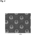
- a SEM photograph of the optical function part 20 is illustrated.
- the optical function part illustrated in Fig. 4 is one in which Au is vapor-deposited as a conductor layer so as to have a thickness of 50 nm on a fine structure part made of a nanoimprint resin having a plurality of pillars (each having a diameter of 120 nm and a height of 180 nm) periodically arranged at a predetermined pitch (a distance of 360 nm between center lines).
- the holding part 4 has a plurality of pinching parts 41 arranged around the optical function part 20 when seen in the thickness direction of the substrate 21 and leg parts 42 extending from the respective pinching parts 41 toward a rear face 3b of the transportation board 3.
- Fitting holes 11 are formed in the front face 3a of the transportation board 3 so as to correspond to the leg parts 42, respectively.
- the leg parts 42 are fitted into their corresponding fitting holes 11 in a state where the pinching parts 41 are in contact with the conductor layer 23 of the SERS element 2.
- the fitting holes 11 do not penetrate through the transportation board 3 but are bottomed.
- the leg parts 42 and fitting holes 11 are formed cylindrical.
- the holding part 4 having the pinching parts 41 and leg parts 42 is integrally formed from materials such as resins (polypropylene, styrol resin, ABS resin, polyethylene, PET, PMMA, silicone, liquid crystal polymer, etc.), ceramics, glass, and silicon by using techniques such as molding, cutting, and etching.
- resins polypropylene, styrol resin, ABS resin, polyethylene, PET, PMMA, silicone, liquid crystal polymer, etc.
- ceramics glass, and silicon by using techniques such as molding, cutting, and etching.
- the holding part 4 formed separately from the transportation board 3 is mechanically secured to the transportation board 3, while the SERS element 2 arranged in the depression 9 is pinched between the transportation board 3 and the pinching parts 41 of the holding part 4.
- mechanically is meant herein “through fitting between members without adhesives and the like.”
- the SERS unit 1A is prepared, and the SERS element 2 is removed from the transportation board 3 (first step). More specifically, the switching parts 41 are rotated around their corresponding leg parts 42 with respect to the transportation board 3, so as to be retracted from above the SERS element 2, whereby the SERS element 2 is taken out of the depression 9 of the transportation board 3.
- the holding part 4 may be removed from the transportation board 3, so as to take the SERS element 2 out of the depression 9 of the transportation board 3.
- a sample is arranged on the optical function part 20 of the SERS element 2 (second step). More specifically, the sample is arranged on the optical function part 20 in the SERS element 20 in a state where the SERS element 2 is placed on a glass slide 61, put into each of a plurality of depressions 62a in a support board 62, or left as it is.
- the SERS element 2 in the above-mentioned state is set to a Raman spectroscopic analyzer 50, the sample arranged on the optical function part 20 is irradiated with excitation light, and Raman-scattered light derived from the sample is detected, so as to perform Raman spectroscopic analysis (third step).
- a Raman spectroscopic analyzer 50 comprising, as illustrated in Fig.
- a stage 51 supporting the SERS element 2 a light source 52 for emitting excitation light, an optical component 53 for effecting collimation, filtering, condensing, and the like necessary for irradiating the optical function part 20 with the excitation light, an optical component 54 for effecting collimation, filtering, and the like necessary for guiding Raman-scattered light to a detector 55, and the detector 55 for detecting the Raman-scattered light will be explained in more detail here.
- a solution sample (or a dispersion of a powder sample in water or in a solution of ethanol) is put in the depressions 62a of the support board 62 on which the SERS element 2 is arranged, while cover slips 63 are brought into close contact with the solution sample in order to reduce the lens effect and the evaporation of the solution sample.
- the solution sample arranged on the optical function part 20 is irradiated with the excitation light emitted from the light source 52 through the optical component 53.
- the stage 51 is moved such that a focal point of the excitation light is located at the optical function part 20.
- the released Raman-scattered light is detected by the detector 55 through the optical component 54, so as to perform Raman spectroscopic analysis.
- the SERS element 2 may be held, so as to be dipped into a solution sample (or a dispersion of a powder sample in water or in a solution of ethanol or the like), lifted up, and then blown to dry.
- a minute amount of a solution sample (or a dispersion of a powder sample in water or in a solution of ethanol or the like) may be dropped on the optical function part 20 and left to dry.
- a powder sample may be dispersed as it is on the optical function part 20.
- the holding part 4 detachably holds the SERS element 2 in the transportation board 3 in the holding part 1A. Consequently, as compared with the case where the SERS element 2 is transported while sticking to a gel pack, a tape, or the like, for example, the optical function part 20 is inhibited from deteriorating because of components contained in the gel pack, ingredients of the sticking part of the tape, or the like.
- the SERS element 2 is pinched between the transportation board 3 and pinching parts 41. This makes it possible to hold the SERS element 2 securely in the transportation board 3. Therefore, the SERS unit 1A can inhibit the SERS element 2 from being damaged and the optical function part 20 from deteriorating during transportation. As a result, the Raman spectroscopic analysis method using the SERS unit 1A can accurately perform the Raman spectroscopic analysis.
- the SERS unit 1A can prevent the molded layer 22 and conductor layer 23 formed on the substrate 21 in the SERS element 2 from peeling from the substrate 21 during transportation.
- the holding part 4 is formed separately from the transportation board 3 and mechanically secured to the transportation board 3. This can simplify the structure of the transportation board 3.
- the optical function part 20 can be inhibited from deteriorating because of ingredients contained in the tackifier or adhesive.
- a plurality of pinching parts 41 are arranged around the optical function part 20. This makes it possible to hold the SERS element 2 stably in the transportation board 3.
- the transportation board 3 is provided with the depression 9 containing a part of the SERS element 2 on the substrate 21 side and restraining the SERS element 2 from moving in directions perpendicular to the thickness direction of the substrate 21. This can position the SERS element 2 with respect to the transportation board 3. This can also more securely prevent the SERS element 2 from shifting from the transportation board 3 and being damaged during transportation.
- the transportation board 3 is formed integrally from a resin. This configuration makes it harder for chipping to occur and thus can more securely inhibit the optical function part 20 from deteriorating because of chipped pieces adhering thereto.
- guide grooves 15 for arranging the respective leg parts 42 of the holding part 4 may be provided in side faces of the depression 9 formed in the transportation board 3. This configuration enables the leg parts 42 to fit into the fitting holes 11 easily and securely.
- the leg parts 42 can also position the SERS element 2.
- the depression 9 can also position the SERS element 2 in the case where the guide grooves 15 are provided.
- the SERS element 2 may be arranged on the front face 3a of the transportation board 3. That is, the lower face of the substrate 21 of the SERS element 2 may abut against the front face 3a of the measurement board 3.
- This configuration can improve the strength of the transportation board 3 by the absence of the depression 9.
- the leg parts 42 of the holding part 4 may be formed with stoppers 42a, respectively. In this configuration, fitting the leg parts 42 into the fitting holes 11 until the stoppers 42a come into contact with the transportation board 3 enables the pinching parts 41 to come into contact with the SERS element 2 and exert a substantially fixed pressure thereon, thereby preventing the pressure from acting more than necessary on the SERS element 2.
- the front face 3a of the transportation board 3 may be provided with depressions 16.
- this configuration enables the pinching parts 41 to be retracted from above the depression 9 of the transportation board 3 to substantially fixed positions. Therefore, when assembling the SERS unit 1A, an operation of rotating the pinching parts 41 around the leg parts 42 so as to make the holding part 4 hold the SERS element 2 can be done efficiently.
- the holding part 4 may engage the transportation board 3 such that the holding parts 41 can advance and retract with respect to the SERS element 2 arranged in the depression 9.
- a plurality of pinching parts 41 may be arranged such as to come into contact with the SERS element 2 in each of areas opposing each other in the ring-shaped region in the outer edge of the SERS element 2.
- a SERS unit 1B differs from the above-mentioned SERS unit 1A mainly in that the pinching part 41 is formed into a ring so as to surround the optical function part 20 when seen in the thickness direction of the substrate 21.
- the holding part 4 has the pinching part 41 formed into a ring so as to surround the optical function part 20 when seen in the thickness direction of the substrate 21 and a plurality of leg parts 42 extending from the pinching part 41 toward the rear face 3b of the transportation board 3. Fitting holes 11 are formed in the front face 3a of the transportation board 3 so as to correspond to the leg parts 42, respectively.
- the leg parts 42 are fitted into their corresponding fitting holes 11 in a state where the pinching part 41 surrounds the optical function part 20 and is in contact with the conductor layer 23 of the SERS element 2.
- the holding part 4 formed separately from the transportation board 3 is mechanically secured to the transportation board 3, while the SERS element 2 arranged in the depression 9 is held between the transportation board 3 and the pinching part 41 of the holding part 4.
- the pinching part 41 is formed such as to have a rectangular outer edge and a circular inner edge when seen in the thickness direction of the substrate 21, while the leg parts 42 extend from four corners of the pinching part 41, respectively, toward the rear face 3b of the transportation board 3. Making the inner edge of the pinching part 41 circular prevents pressures from acting locally on the SERS element 2.
- the leg parts 42 and fitting holes 11 are formed cylindrical.
- the holding part 4 having the pinching part 41 and leg parts 42 is integrally formed from materials such as resins (polypropylene, styrol resin, ABS resin, polyethylene, PET, PMMA, silicone, liquid crystal polymer, etc.), ceramics, glass, and silicon by using techniques such as molding, cutting, and etching.
- the SERS unit 1B constructed as in the foregoing can inhibit the SERS element 2 from being damaged and deteriorating during transportation as with the above-mentioned SERS unit 1A.
- the SERS element 2 can be taken out of the transportation board 3 by removing the holding part 4 from the transportation board 3.
- the pinching part 41 is formed into a ring so as to surround the optical function part 20 when seen in the thickness direction of the substrate 21. This can hold the SERS element 2 stably in the transportation board 3.
- the pinching part 41 of the holding part 4 may be formed such as to have a rectangular inner edge when seen in the thickness direction of the substrate 21.
- the pinching part 41 may be formed such as to come into contact with the SERS element 2 in the ring-shaped region in its inner edge.
- the pinching part 41 may be formed such as to come into contact with the SERS element 2 in areas opposing each other in the ring-shaped region in its inner edge.
- the pinching part 41 may be formed such as to come into contact with the SERS element 2 at a plurality of projections 41b formed in its inner edge.
- one of parts opposing each other in the ring-shaped pinching part 41 may be rotatably supported by the transportation board 3, while the other is adapted to engage the transportation board 3.
- This configuration makes it possible to manage the transportation board 3 and holding part 4 in a state where the holding part 4 is attached to the transportation board 3.
- arranging the SERS element 2 in the depression 9 in a state where the holding part 4 is open and then closing the holding part 4 and making the other part of the pinching part 41 engage the transportation board 3 enables the holding part 4 to hold the SERS element 2 easily.
- the SERS element 2 can be removed from the transportation board 3 in a procedure reversed from that of assembling the SERS unit 1B.
- a spring may be installed between the one part of the holding part 4 and the transportation board 3.
- the holding part 4 may have a projection 43 projecting outward from the pinching part 41 or leg part 42 while forming a gap between the holding part 4 and the front face 3a of the transportation board 3. This configuration makes it easy to remove the holding part 4 from the transportation board 3 by catching the projection 43 with a jig or the like.
- the holding part 4 may have a cover 44 for covering the opening of the pinching part 41 formed into a ring. This configuration can prevent the optical function part 20 from being damaged and so forth because of some members coming into contact with the optical function part 20 during transportation.
- the projection 43 may be formed either integrally with or separately from the pinching part 41 or leg part 42.
- the cover 44 may be formed either integrally with or separately from the pinching part 41.
- a SERS unit 1C differs from the above-mentioned SERS unit 1A mainly in that the holding part 4 is integrally formed with the transportation board 3.
- the holding part 4 is deformed so as to open each pinching part 41 as illustrated in Fig. 18(a) , whereby the SERS element 2 is arranged in the transportation board 3, and then the deformed holding part 4 is returned to its original state so as to close each pinching part 41 as illustrated in Fig. 18(b) , thereby making the holding part 4 hold the SERS element 2.
- the SERS unit 1C constructed as in the foregoing can inhibit the SERS element 2 from being damaged and the optical function part 20 from deteriorating during transportation as with the above-mentioned SERS unit 1A.
- the SERS element 2 can be removed from the transportation board 3 in a procedure reversed from that of assembling the SERS unit 1C.
- the holding part 4 is formed integrally with the transportation board 3. This can reduce the number of components in the SERS unit 1C.
- the optical function part 20 can be inhibited from deteriorating because of ingredients contained in the tackifier or adhesive.
- each pinching part 41 may have a tilted surface 41 formed so as to widen toward the side opposite from the transportation board 3. This configuration can easily guide the SERS element 2 to its holding position in the transportation board 3 when assembling the SERS unit 1C.
- each pinching part 41 may have a tilted surface 41d formed so as to widen toward the transportation board 3. This configuration can facilitate an operation of deforming the holding part 4 so as to open each pinching part 41 when assembling the SERS unit 1C and when removing the SERS element 2 from the transportation board 3 upon measurement.
- Fig. 19 each pinching part 41 may have a tilted surface 41 formed so as to widen toward the side opposite from the transportation board 3. This configuration can easily guide the SERS element 2 to its holding position in the transportation board 3 when assembling the SERS unit 1C.
- each pinching part 41 may have a tilted surface 41d formed so as to widen toward the transportation board 3. This configuration can facilitate an operation of deforming the holding part 4 so as to open each pinching part 41 when assembling the SERS
- each pinching part 41 may have a cutout 41e for engaging a jig 60 used for the operation of deforming the holding part 4 so as to open each pinching part 41.
- This configuration can facilitate the operation of deforming the holding part 4 so as to open each pinching part 41 by using the jig 60, while securely preventing the jig 60 from coming into contact with the optical function part 20 when assembling the SERS unit 1C and when removing the SERS element 2 from the transportation board 3 upon measurement.
- a plurality of SERS elements 2 may be arranged on the transportation board 3 and detachably held by the holding part 4 in a SERS unit 1D.
- the holding part 4 may be integrally formed with all the SERS elements 2. This configuration makes it possible to remove all the SERS elements 2 collectively from the transportation board 3.
- the holding part 4 may be divided into groups of a plurality of SERS elements 2 as illustrated in Fig. 22(b) or into the respective SERS elements 2 as illustrated in Fig. 22(c) . These configurations make it possible to remove a specific number of SERS elements 2 or one SERS element 2 from the transportation board 3.
- the transportation board 3 and holding part 4 may be constructed so as to be dividable.
- the transportation board 3 integrally formed for all the SERS elements 2 may be provided with grooves 17 for dividing the transportation board 3 into the respective SERS elements 2 (or into groups of a plurality of SERS elements 2), while a plurality of holding parts 4 are formed for the respective SERS elements 2 (or for the respective groups of a plurality of SERS elements 2).
- the holding part 4 integrally formed for all the SERS elements 2 may be provided with grooves 18 for dividing the holding part 4 into the respective SERS elements 2 (or into groups of a plurality of SERS elements 2), while a plurality of transportation boards 3 are formed for the respective SERS elements 2 (or for the respective groups of a plurality of SERS elements 2).
- Fig. 1 the holding part 4 integrally formed for all the SERS elements 2 may be provided with grooves 18 for dividing the holding part 4 into the respective SERS elements 2 (or into groups of a plurality of SERS elements 2), while a plurality of transportation boards 3 are formed for the respective SERS elements 2 (or for the respective groups of a plurality of SERS elements 2).
- the transportation board 3 integrally formed for all the SERS elements 2 may be provided with grooves 17 for dividing the transportation board 3 into the respective SERS elements 2 (or into groups of a plurality of SERS elements 2), while the holding part 4 integrally formed for all the SERS elements 2 is provided with grooves 18 for dividing the holding part 4 into the respective SERS elements 2 (or into groups of a plurality of SERS elements 2).
- the material for the transportation board 3 is not limited to resins, but may be low-melting glass, ceramics, and the like.
- the transportation board 3 can be formed by integral molding from low-melting glass as from a resin. From a ceramic, the transportation board 3 can be formed by firing.
- Various materials and forms in addition to those mentioned above can be employed for the structures of the SERS units 1A to 1D.
- the ring shape is not limited to circular rings, but encompasses other ring shapes such as rectangular rings.
- the fine structure part 24 may be formed on the front face 21a of the substrate 21 either indirectly with the support part 25, for example, interposed therebetween or directly.
- the conductor layer 23 is not limited to the one directly formed on the fine structure part 24, but may indirectly be formed on the fine structure part 24 through some layers such as layers of buffer metals (Ti, Cr, and the like) for improving the adhesion of the metal to the fine structure part 24.
- the present invention can provide a surface-enhanced Raman scattering unit which can inhibit the surface-enhanced Raman scattering element from being damaged and the optical function part from deteriorating during transportation and a Raman spectroscopic analysis method using such a surface-enhanced Raman scattering unit.
- 1A, 1B, 1C, 1D SERS unit (surface-enhanced Raman scattering unit); 2: SERS element (surface-enhanced Raman scattering element); 3: transportation board; 4: holding part; 9: depression; 20: optical function part; 21: substrate; 41: pinching part.
Landscapes
- Health & Medical Sciences (AREA)
- Physics & Mathematics (AREA)
- Chemical & Material Sciences (AREA)
- General Physics & Mathematics (AREA)
- Analytical Chemistry (AREA)
- Biochemistry (AREA)
- Life Sciences & Earth Sciences (AREA)
- Nuclear Medicine, Radiotherapy & Molecular Imaging (AREA)
- General Health & Medical Sciences (AREA)
- Immunology (AREA)
- Pathology (AREA)
- Chemical Kinetics & Catalysis (AREA)
- Clinical Laboratory Science (AREA)
- Optics & Photonics (AREA)
- Investigating, Analyzing Materials By Fluorescence Or Luminescence (AREA)
- Optical Measuring Cells (AREA)
Abstract
Description
- The present invention relates to a surface-enhanced Raman scattering unit and a Raman spectroscopic analysis method.
- Known as a conventional surface-enhanced Raman scattering unit is one in which a surface-enhanced Raman scattering element having an optical function part for generating surface-enhanced Raman scattering (SERS) is secured onto a glass slide (see, for example, Non Patent Literature 1).
- Non Patent Literature 1: "Q-SERS™ G1 Substrate", [online], Opto Science, Inc., [retrieved on 2013-03-21]. Retrieved from the Internet: < URL: http://www.optoscience.com/maker/nanova/pdf/Q-SERS_G1.pdf>.
- While a surface-enhanced Raman scattering unit such as the one mentioned above is set to a Raman spectroscopic analyzer in a unit state (i.e., a state where the surface-enhanced Raman scattering element is secured onto the glass slide), the surface-enhanced Raman scattering element prepared alone may be set to the Raman spectroscopic analyzer as being arranged on a substrate prepared separately or as it is. In such a case, it is necessary for the surface-enhanced Raman scattering element to be transported alone. When the surface-enhanced Raman scattering element is transported while sticking to a gel pack, a tape, or the like in order to prevent it from being damaged, however, the optical function part may deteriorate because of components contained in the gel pack, ingredients of the bonding part of the tape, or the like. When transported as being mounted on an IC chip tray with a cover tray put thereon, on the other hand, the surface-enhanced Raman scattering element may be chipped or damaged because of vibrations during transportation and the like.
- It is therefore an object of the present invention to provide a surface-enhanced Raman scattering unit which can inhibit the surface-enhanced Raman scattering element from being damaged and the optical function part from deteriorating during transportation and a Raman spectroscopic analysis method using such a surface-enhanced Raman scattering unit.
- The surface-enhanced Raman scattering unit in accordance with one aspect of the present invention comprises a surface-enhanced Raman scattering element having a substrate and an optical function part formed on the substrate, the optical function part for generating surface-enhanced Raman scattering; a transportation board supporting the surface-enhanced Raman scattering element during transportation, the surface-enhanced Raman scattering element being removed from the transportation board upon measurement; and a holding part having a pinching part pinching the surface-enhanced Raman scattering element in cooperation with the transportation board, and detachably holding the surface-enhanced Raman scattering element in the transportation board.
- In this surface-enhanced Raman scattering unit, the holding part detachably holds the surface-enhanced Raman scattering element in the transportation board. If the surface-enhanced Raman scattering element is transported while sticking to a gel pack, a tape, or the like, deterioration will progress in the optical function part during transportation because of components contained in the gel pack, ingredients of the sticking part of the tape, or the like. However, this surface-enhanced Raman scattering unit does not use tackifiers and/or adhesives of gel packs or tapes and thus can inhibit the optical function part from deteriorating. In addition, the surface-enhanced Raman scattering element is pinched between the transportation board and pinching part. This can hold the surface-enhanced Raman scattering element securely in the transportation board. Therefore, this surface-enhanced Raman scattering unit can inhibit the surface-enhanced Raman scattering element from being damaged and the optical function part from deteriorating during transportation.
- In the surface-enhanced Raman scattering unit in accordance with one aspect of the present invention, the holding part may be formed separately from the transportation board and mechanically secured to the transportation board. This configuration can simplify the structure of the transportation board. In addition, as compared with the case where the holding part is secured to the transportation board with a tackifier or adhesive, for example, the optical function part can be inhibited from deteriorating because of ingredients contained in the tackifier or adhesive.
- In the surface-enhanced Raman scattering unit in accordance with one aspect of the present invention, the holding part may be formed integrally with the transportation board. This configuration can reduce the number of components in the surface-enhanced Raman scattering unit. In addition, as compared with the case where the holding part is secured to the transportation board with a tackifier or adhesive, for example, the optical function part can be inhibited from deteriorating because of ingredients contained in the tackifier or adhesive.
- In the surface-enhanced Raman scattering unit in accordance with one aspect of the present invention, the pinching part may be formed into a ring so as to surround the optical function part when seen in a thickness direction of the substrate, or a plurality of pinching parts may be arranged around the optical function part. These configurations can stably hold the surface-enhanced Raman scattering element in the transportation board.
- In the surface-enhanced Raman scattering unit in accordance with one aspect of the present invention, the transportation board may be provided with a depression containing at least a part of the surface-enhanced Raman scattering element on the substrate side and restraining the surface-enhanced Raman scattering element from moving in a direction perpendicular to the thickness direction of the substrate. This configuration can position the surface-enhanced Raman scattering element with respect to the transportation board. This can also more securely prevent the surface-enhanced Raman scattering element from shifting from the transportation board and being damaged during transportation.
- In the surface-enhanced Raman scattering unit in accordance with one aspect of the present invention, the transportation board may be formed integrally from a resin. This configuration makes it harder for chipping to occur and thus can more securely inhibit the optical function part from deteriorating because of chipped pieces adhering thereto.
- A Raman spectroscopic analysis method in accordance with one aspect of the present invention comprises a first step of preparing the above-mentioned surface-enhanced Raman scattering unit and removing the surface-enhanced Raman scattering element from the transportation board; a second step, after the first step, of arranging a sample on the optical function part of the surface-enhanced Raman scattering element; and a third step, after the second step, of setting the surface-enhanced Raman scattering element to a Raman spectroscopic analyzer, irradiating the sample arranged on the optical function part with excitation light, and detecting Raman-scattered light derived from the sample, so as to perform Raman spectroscopic analysis.
- This Raman spectroscopic analysis method uses the surface-enhanced Raman scattering element transported as the above-mentioned surface-enhanced Raman scattering unit and thus can perform the Raman spectroscopic analysis accurately.
- The present invention can provide a surface-enhanced Raman scattering unit which can inhibit the surface-enhanced Raman scattering element from being damaged and the optical function part from deteriorating during transportation and a Raman spectroscopic analysis method using such a surface-enhanced Raman scattering unit.
-
-
Fig. 1 is a plan view of the surface-enhanced Raman scattering unit in accordance with a first embodiment of the present invention; -
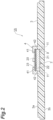
Fig. 2 is a sectional view of the surface-enhanced Raman scattering unit taken along the line II-II ofFig. 1 ; -
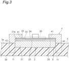
Fig. 3 is a partly enlarged sectional view of the surface-enhanced Raman scattering unit taken along the line II-II ofFig. 1 ; -
Fig. 4 is a SEM photograph of an optical function part in the surface-enhanced Raman scattering unit ofFig. 1 ; -
Fig. 5 is a diagram illustrating a procedure of Raman spectroscopic analysis using the surface-enhanced Raman scattering unit ofFig. 1 ; -
Fig. 6 is a diagram illustrating the procedure of Raman spectroscopic analysis using the surface-enhanced Raman scattering unit ofFig. 1 ; -
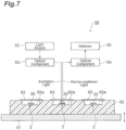
Fig. 7 is a structural diagram of a Raman spectroscopic analyzer to which the surface-enhanced Raman scattering unit ofFig. 1 is set; -
Fig. 8 is a partly enlarged sectional view of a modified example of the surface-enhanced Raman scattering unit ofFig. 1 ; -
Fig. 9 is a partly enlarged sectional view of modified examples of the surface-enhanced Raman scattering unit ofFig. 1 ; -
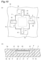
Fig. 10 is a set of partly enlarged plan and sectional views of a modified example of the surface-enhanced Raman scattering unit ofFig. 1 ; -
Fig. 11 is a set of partly enlarged plan and sectional views of a modified example of the surface-enhanced Raman scattering unit ofFig. 1 ; -
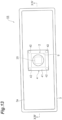
Fig. 12 is a partly enlarged plan view of a modified example of the surface-enhanced Raman scattering unit ofFig. 1 ; -
Fig. 13 is a plan view of the surface-enhanced Raman scattering unit in accordance with a second embodiment of the present invention; -
Fig. 14 is a sectional view of the surface-enhanced Raman scattering unit taken along the line XIV-XIV ofFig. 13 ; -
Fig. 15 is a partly enlarged plan view of modified examples of the surface-enhanced Raman scattering unit ofFig. 13 ; -
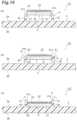
Fig. 16 is a set of partly enlarged plan and sectional views of a modified example of the surface-enhanced Raman scattering unit ofFig. 13 ; -
Fig. 17 is a partly enlarged sectional view of modified examples of the surface-enhanced Raman scattering unit ofFig. 13 ; -
Fig. 18 is a partly enlarged sectional view of the surface-enhanced Raman scattering unit in accordance with a third embodiment of the present invention; -
Fig. 19 is a partly enlarged sectional view of a modified example of the surface-enhanced Raman scattering unit ofFig. 18 ; -
Fig. 20 is a partly enlarged sectional view of a modified example of the surface-enhanced Raman scattering unit ofFig. 18 ; -
Fig. 21 is a partly enlarged sectional view of a modified example of the surface-enhanced Raman scattering unit ofFig. 18 ; -
Fig. 22 is a perspective view of surface-enhanced Raman scattering units in accordance with other embodiments of the present invention; and -
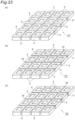
Fig. 23 is a perspective view of surface-enhanced Raman scattering units in accordance with still other embodiments of the present invention. - In the following, preferred embodiments of the present invention will be explained in detail with reference to the drawings. In the drawings, the same or equivalent constituents will be referred to with the same signs while omitting their overlapping descriptions.
- As illustrated in
Figs. 1 and2 , a SERS unit (surface-enhanced Raman scattering unit) 1A comprises a SERS element (surface-enhanced Raman scattering element) 2, atransportation board 3 supporting theSERS element 2, and a holdingpart 4 detachably holding theSERS element 2 in thetransportation board 3. Thetransportation board 3 supports theSERS element 2 during transportation, and theSERS element 2 is removed from thetransportation board 3 upon measurement. - The
transportation board 3 has afront face 3a provided with adepression 9 containing a part of theSERS element 2 on asubstrate 21 side. Thedepression 9 is formed complementary to a part of theSERS element 2 on thesubstrate 21 side and restrains theSERS element 2 from moving in directions perpendicular to the thickness direction of thesubstrate 21. TheSERS element 2 is not secured to the inner surface of thedepression 9 with an adhesive or the like, but is only in contact with the inner surface of thedepression 9. For example, thetransportation board 3 is formed into a rectangular plate. Thedepression 9 is formed into a rectangular parallelepiped. Thetransportation board 3 is integrally formed from materials such as resins (polypropylene, styrol resin, ABS resin, polyethylene, PET, PMMA, silicone, liquid crystal polymer, etc.), ceramics, glass, and silicon by using techniques such as molding, cutting, and etching. - As illustrated in
Fig. 3 , theSERS element 2 comprises asubstrate 21, a moldedlayer 22 formed on thesubstrate 21, and aconductor layer 23 formed on the moldedlayer 22. For example, thesubstrate 21 is formed from silicon, glass, or the like into a rectangular plate having an outer form on the order of several hundred µm × several hundred µm to several ten mm × several ten mm and a thickness on the order of 100 µm to 2 mm. - The molded
layer 22 has afine structure part 24, asupport part 25, and aframe part 26. Thefine structure part 24, which is a region having a periodic pattern, is formed on a surface layer opposite from thesubstrate 21 at a center part of the moldedlayer 22. As the periodic pattern, a plurality of pillars each having a thickness and height on the order of several nm to several hundred nm are periodically arranged at a pitch on the order of several ten nm to several hundred nm in thefine structure part 24. Thesupport part 25, which is a region supporting thefine structure part 24, is formed on afront face 21a of thesubstrate 21. Theframe part 26, which is a ring-shaped region surrounding thesupport part 25, is formed on thefront face 21a of thesubstrate 21. - For example, the
fine structure part 24 has a rectangular outer form on the order of several hundred µm × several hundred µm to several ten mm × several ten mm when seen from one side in the thickness direction of thetransportation board 3. Thesupport part 25 andframe part 26 have a thickness on the order of several ten nm to several ten µm. The moldedlayer 22 is integrally formed by molding a resin (examples of which include resins based on acrylics, fluorine, epoxy, silicone, and urethane, PET, polycarbonate, and inorganic/organic hybrid materials) or low-melting glass arranged on thesubstrate 21 by nanoimprinting, for example. - The
conductor layer 23 is formed over thefine structure part 24 to theframe part 26. In thefine structure part 24, theconductor layer 23 reaches a surface of thesupport part 25, exposed to the side opposite from thesubstrate 21. For example, theconductor layer 23 has a thickness on the order of several nm to several µm. Theconductor layer 23 is formed by vapor-depositing a conductor such as a metal (Au, Ag, Al, Cu, Pt, or the like) on the moldedlayer 22 molded by nanoimprinting, for example. - In the
SERS element 2, theconductor layer 23 formed over the surface of thefine structure part 24 and the surface of thesupport part 25 exposed to the side opposite from thesubstrate 21 produces anoptical function part 20, which generates surface-enhanced Raman scattering, on thesubstrate 21. For reference, a SEM photograph of theoptical function part 20 is illustrated. The optical function part illustrated inFig. 4 is one in which Au is vapor-deposited as a conductor layer so as to have a thickness of 50 nm on a fine structure part made of a nanoimprint resin having a plurality of pillars (each having a diameter of 120 nm and a height of 180 nm) periodically arranged at a predetermined pitch (a distance of 360 nm between center lines). - As illustrated in
Figs. 1 ,2 , and3 , the holdingpart 4 has a plurality of pinchingparts 41 arranged around theoptical function part 20 when seen in the thickness direction of thesubstrate 21 andleg parts 42 extending from therespective pinching parts 41 toward arear face 3b of thetransportation board 3. Fittingholes 11 are formed in thefront face 3a of thetransportation board 3 so as to correspond to theleg parts 42, respectively. Theleg parts 42 are fitted into their corresponding fitting holes 11 in a state where the pinchingparts 41 are in contact with theconductor layer 23 of theSERS element 2. The fitting holes 11 do not penetrate through thetransportation board 3 but are bottomed. For example, theleg parts 42 andfitting holes 11 are formed cylindrical. The holdingpart 4 having the pinchingparts 41 andleg parts 42 is integrally formed from materials such as resins (polypropylene, styrol resin, ABS resin, polyethylene, PET, PMMA, silicone, liquid crystal polymer, etc.), ceramics, glass, and silicon by using techniques such as molding, cutting, and etching. - Thus, the holding
part 4 formed separately from thetransportation board 3 is mechanically secured to thetransportation board 3, while theSERS element 2 arranged in thedepression 9 is pinched between thetransportation board 3 and the pinchingparts 41 of the holdingpart 4. By "mechanically" is meant herein "through fitting between members without adhesives and the like." - A Raman spectroscopic analysis method using the
SERS unit 1A will now be explained. First, as illustrated inFig. 5 , theSERS unit 1A is prepared, and theSERS element 2 is removed from the transportation board 3 (first step). More specifically, the switchingparts 41 are rotated around theircorresponding leg parts 42 with respect to thetransportation board 3, so as to be retracted from above theSERS element 2, whereby theSERS element 2 is taken out of thedepression 9 of thetransportation board 3. The holdingpart 4 may be removed from thetransportation board 3, so as to take theSERS element 2 out of thedepression 9 of thetransportation board 3. - Then, as illustrated in
Fig. 6 , a sample is arranged on theoptical function part 20 of the SERS element 2 (second step). More specifically, the sample is arranged on theoptical function part 20 in theSERS element 20 in a state where theSERS element 2 is placed on aglass slide 61, put into each of a plurality ofdepressions 62a in asupport board 62, or left as it is. - Thereafter, the
SERS element 2 in the above-mentioned state is set to aRaman spectroscopic analyzer 50, the sample arranged on theoptical function part 20 is irradiated with excitation light, and Raman-scattered light derived from the sample is detected, so as to perform Raman spectroscopic analysis (third step). A case where the Raman spectroscopic analysis is performed in theRaman spectroscopic analyzer 50 comprising, as illustrated inFig. 7 , astage 51 supporting theSERS element 2, alight source 52 for emitting excitation light, anoptical component 53 for effecting collimation, filtering, condensing, and the like necessary for irradiating theoptical function part 20 with the excitation light, anoptical component 54 for effecting collimation, filtering, and the like necessary for guiding Raman-scattered light to adetector 55, and thedetector 55 for detecting the Raman-scattered light will be explained in more detail here. - For example, a solution sample (or a dispersion of a powder sample in water or in a solution of ethanol) is put in the
depressions 62a of thesupport board 62 on which theSERS element 2 is arranged, while cover slips 63 are brought into close contact with the solution sample in order to reduce the lens effect and the evaporation of the solution sample. In this state, the solution sample arranged on theoptical function part 20 is irradiated with the excitation light emitted from thelight source 52 through theoptical component 53. At this time, thestage 51 is moved such that a focal point of the excitation light is located at theoptical function part 20. This causes surface-enhanced Raman scattering at the interface between theoptical function part 20 and the solution sample, whereby Raman-scattered light derived from the solution sample is released after being enhanced by about 108 times, for example. The released Raman-scattered light is detected by thedetector 55 through theoptical component 54, so as to perform Raman spectroscopic analysis. - Not only the above-mentioned method but the following methods may also be used for arranging the sample on the
optical function part 20. For example, theSERS element 2 may be held, so as to be dipped into a solution sample (or a dispersion of a powder sample in water or in a solution of ethanol or the like), lifted up, and then blown to dry. A minute amount of a solution sample (or a dispersion of a powder sample in water or in a solution of ethanol or the like) may be dropped on theoptical function part 20 and left to dry. A powder sample may be dispersed as it is on theoptical function part 20. - Effects exhibited by the
SERS unit 1A will now be explained. First, the holdingpart 4 detachably holds theSERS element 2 in thetransportation board 3 in the holdingpart 1A. Consequently, as compared with the case where theSERS element 2 is transported while sticking to a gel pack, a tape, or the like, for example, theoptical function part 20 is inhibited from deteriorating because of components contained in the gel pack, ingredients of the sticking part of the tape, or the like. In addition, theSERS element 2 is pinched between thetransportation board 3 and pinchingparts 41. This makes it possible to hold theSERS element 2 securely in thetransportation board 3. Therefore, theSERS unit 1A can inhibit theSERS element 2 from being damaged and theoptical function part 20 from deteriorating during transportation. As a result, the Raman spectroscopic analysis method using theSERS unit 1A can accurately perform the Raman spectroscopic analysis. - Since the
SERS element 2 is pinched between thetransportation board 3 and pinchingparts 41, theSERS unit 1A can prevent the moldedlayer 22 andconductor layer 23 formed on thesubstrate 21 in theSERS element 2 from peeling from thesubstrate 21 during transportation. - In the
SERS unit 1A, the holdingpart 4 is formed separately from thetransportation board 3 and mechanically secured to thetransportation board 3. This can simplify the structure of thetransportation board 3. In addition, as compared with the case where the holdingpart 4 is secured to thetransportation board 3 with a tackifier or adhesive, for example, theoptical function part 20 can be inhibited from deteriorating because of ingredients contained in the tackifier or adhesive. - In the
SERS unit 1A, a plurality of pinchingparts 41 are arranged around theoptical function part 20. This makes it possible to hold theSERS element 2 stably in thetransportation board 3. - In the
SERS unit 1A, thetransportation board 3 is provided with thedepression 9 containing a part of theSERS element 2 on thesubstrate 21 side and restraining theSERS element 2 from moving in directions perpendicular to the thickness direction of thesubstrate 21. This can position theSERS element 2 with respect to thetransportation board 3. This can also more securely prevent theSERS element 2 from shifting from thetransportation board 3 and being damaged during transportation. - In the
SERS unit 1A, thetransportation board 3 is formed integrally from a resin. This configuration makes it harder for chipping to occur and thus can more securely inhibit theoptical function part 20 from deteriorating because of chipped pieces adhering thereto. - Modified examples of the
SERS unit 1A will now be explained. As illustrated inFig. 8(a) , guidegrooves 15 for arranging therespective leg parts 42 of the holdingpart 4 may be provided in side faces of thedepression 9 formed in thetransportation board 3. This configuration enables theleg parts 42 to fit into the fitting holes 11 easily and securely. In this case, theleg parts 42 can also position theSERS element 2. As illustrated inFig. 8(b) , thedepression 9 can also position theSERS element 2 in the case where theguide grooves 15 are provided. - As illustrated in
Fig. 9(a) , theSERS element 2 may be arranged on thefront face 3a of thetransportation board 3. That is, the lower face of thesubstrate 21 of theSERS element 2 may abut against thefront face 3a of themeasurement board 3. This configuration can improve the strength of thetransportation board 3 by the absence of thedepression 9. As illustrated inFig. 9(b) , theleg parts 42 of the holdingpart 4 may be formed withstoppers 42a, respectively. In this configuration, fitting theleg parts 42 into the fitting holes 11 until thestoppers 42a come into contact with thetransportation board 3 enables the pinchingparts 41 to come into contact with theSERS element 2 and exert a substantially fixed pressure thereon, thereby preventing the pressure from acting more than necessary on theSERS element 2. - As illustrated in
Fig. 10 , for restricting rotation areas of the pinchingparts 41 when the pinchingparts 41 are rotated around theleg parts 42 with respect to thetransportation board 3, thefront face 3a of thetransportation board 3 may be provided withdepressions 16. At a stage prior to assembling theSERS unit 1A, this configuration enables the pinchingparts 41 to be retracted from above thedepression 9 of thetransportation board 3 to substantially fixed positions. Therefore, when assembling theSERS unit 1A, an operation of rotating the pinchingparts 41 around theleg parts 42 so as to make the holdingpart 4 hold theSERS element 2 can be done efficiently. - As illustrated in
Fig. 11 , the holdingpart 4 may engage thetransportation board 3 such that the holdingparts 41 can advance and retract with respect to theSERS element 2 arranged in thedepression 9. As illustrated inFig. 12 , a plurality of pinchingparts 41 may be arranged such as to come into contact with theSERS element 2 in each of areas opposing each other in the ring-shaped region in the outer edge of theSERS element 2. - As illustrated in
Figs. 13 and14 , aSERS unit 1B differs from the above-mentionedSERS unit 1A mainly in that the pinchingpart 41 is formed into a ring so as to surround theoptical function part 20 when seen in the thickness direction of thesubstrate 21. In theSERS unit 1B, the holdingpart 4 has the pinchingpart 41 formed into a ring so as to surround theoptical function part 20 when seen in the thickness direction of thesubstrate 21 and a plurality ofleg parts 42 extending from the pinchingpart 41 toward therear face 3b of thetransportation board 3. Fittingholes 11 are formed in thefront face 3a of thetransportation board 3 so as to correspond to theleg parts 42, respectively. Theleg parts 42 are fitted into their corresponding fitting holes 11 in a state where the pinchingpart 41 surrounds theoptical function part 20 and is in contact with theconductor layer 23 of theSERS element 2. Thus, the holdingpart 4 formed separately from thetransportation board 3 is mechanically secured to thetransportation board 3, while theSERS element 2 arranged in thedepression 9 is held between thetransportation board 3 and the pinchingpart 41 of the holdingpart 4. - For example, the pinching
part 41 is formed such as to have a rectangular outer edge and a circular inner edge when seen in the thickness direction of thesubstrate 21, while theleg parts 42 extend from four corners of the pinchingpart 41, respectively, toward therear face 3b of thetransportation board 3. Making the inner edge of the pinchingpart 41 circular prevents pressures from acting locally on theSERS element 2. Theleg parts 42 andfitting holes 11 are formed cylindrical. The holdingpart 4 having the pinchingpart 41 andleg parts 42 is integrally formed from materials such as resins (polypropylene, styrol resin, ABS resin, polyethylene, PET, PMMA, silicone, liquid crystal polymer, etc.), ceramics, glass, and silicon by using techniques such as molding, cutting, and etching. - The
SERS unit 1B constructed as in the foregoing can inhibit theSERS element 2 from being damaged and deteriorating during transportation as with the above-mentionedSERS unit 1A. Upon measurement, theSERS element 2 can be taken out of thetransportation board 3 by removing the holdingpart 4 from thetransportation board 3. - In the
SERS unit 1B, the pinchingpart 41 is formed into a ring so as to surround theoptical function part 20 when seen in the thickness direction of thesubstrate 21. This can hold theSERS element 2 stably in thetransportation board 3. - Modified examples of the
SERS unit 1B will now be explained. As illustrated inFig. 15 , the pinchingpart 41 of the holdingpart 4 may be formed such as to have a rectangular inner edge when seen in the thickness direction of thesubstrate 21. As illustrated inFig. 15(a) , the pinchingpart 41 may be formed such as to come into contact with theSERS element 2 in the ring-shaped region in its inner edge. As illustrated inFig. 15(b) , the pinchingpart 41 may be formed such as to come into contact with theSERS element 2 in areas opposing each other in the ring-shaped region in its inner edge. As illustrated inFig. 15(c) , the pinchingpart 41 may be formed such as to come into contact with theSERS element 2 at a plurality ofprojections 41b formed in its inner edge. - As illustrated in
Fig. 16 , one of parts opposing each other in the ring-shaped pinchingpart 41 may be rotatably supported by thetransportation board 3, while the other is adapted to engage thetransportation board 3. This configuration makes it possible to manage thetransportation board 3 and holdingpart 4 in a state where the holdingpart 4 is attached to thetransportation board 3. When assembling theSERS unit 1B, arranging theSERS element 2 in thedepression 9 in a state where the holdingpart 4 is open and then closing the holdingpart 4 and making the other part of the pinchingpart 41 engage thetransportation board 3 enables the holdingpart 4 to hold theSERS element 2 easily. Upon measurement, theSERS element 2 can be removed from thetransportation board 3 in a procedure reversed from that of assembling theSERS unit 1B. For making it easier to open and close the holdingpart 4, a spring may be installed between the one part of the holdingpart 4 and thetransportation board 3. - As illustrated in
Fig. 17(a) , the holdingpart 4 may have aprojection 43 projecting outward from the pinchingpart 41 orleg part 42 while forming a gap between the holdingpart 4 and thefront face 3a of thetransportation board 3. This configuration makes it easy to remove the holdingpart 4 from thetransportation board 3 by catching theprojection 43 with a jig or the like. As illustrated inFig. 17(b) , the holdingpart 4 may have acover 44 for covering the opening of the pinchingpart 41 formed into a ring. This configuration can prevent theoptical function part 20 from being damaged and so forth because of some members coming into contact with theoptical function part 20 during transportation. Theprojection 43 may be formed either integrally with or separately from the pinchingpart 41 orleg part 42. Similarly, thecover 44 may be formed either integrally with or separately from the pinchingpart 41. - As illustrated in
Fig. 18 , aSERS unit 1C differs from the above-mentionedSERS unit 1A mainly in that the holdingpart 4 is integrally formed with thetransportation board 3. When assembling theSERS unit 1C, the holdingpart 4 is deformed so as to open each pinchingpart 41 as illustrated inFig. 18(a) , whereby theSERS element 2 is arranged in thetransportation board 3, and then thedeformed holding part 4 is returned to its original state so as to close each pinchingpart 41 as illustrated inFig. 18(b) , thereby making the holdingpart 4 hold theSERS element 2. - The
SERS unit 1C constructed as in the foregoing can inhibit theSERS element 2 from being damaged and theoptical function part 20 from deteriorating during transportation as with the above-mentionedSERS unit 1A. Upon measurement, theSERS element 2 can be removed from thetransportation board 3 in a procedure reversed from that of assembling theSERS unit 1C. - In the
SERS unit 1C, the holdingpart 4 is formed integrally with thetransportation board 3. This can reduce the number of components in theSERS unit 1C. In addition, as compared with the case where the holdingpart 4 is secured to thetransportation board 3 with a tackifier or adhesive, for example, theoptical function part 20 can be inhibited from deteriorating because of ingredients contained in the tackifier or adhesive. - Modified examples of the
SERS unit 1C will now be explained. As illustrated inFig. 19 , each pinchingpart 41 may have a tiltedsurface 41 formed so as to widen toward the side opposite from thetransportation board 3. This configuration can easily guide theSERS element 2 to its holding position in thetransportation board 3 when assembling theSERS unit 1C. As illustrated inFig. 20 , each pinchingpart 41 may have a tiltedsurface 41d formed so as to widen toward thetransportation board 3. This configuration can facilitate an operation of deforming the holdingpart 4 so as to open each pinchingpart 41 when assembling theSERS unit 1C and when removing theSERS element 2 from thetransportation board 3 upon measurement. As illustrated inFig. 21 , each pinchingpart 41 may have acutout 41e for engaging ajig 60 used for the operation of deforming the holdingpart 4 so as to open each pinchingpart 41. This configuration can facilitate the operation of deforming the holdingpart 4 so as to open each pinchingpart 41 by using thejig 60, while securely preventing thejig 60 from coming into contact with theoptical function part 20 when assembling theSERS unit 1C and when removing theSERS element 2 from thetransportation board 3 upon measurement. - While the first to third embodiments of the present invention are explained in the foregoing, the present invention is not limited to the above-mentioned embodiments. For example, as illustrated in
Fig. 22 , a plurality ofSERS elements 2 may be arranged on thetransportation board 3 and detachably held by the holdingpart 4 in aSERS unit 1D. As illustrated inFig. 22(a) , the holdingpart 4 may be integrally formed with all theSERS elements 2. This configuration makes it possible to remove all theSERS elements 2 collectively from thetransportation board 3. The holdingpart 4 may be divided into groups of a plurality ofSERS elements 2 as illustrated inFig. 22(b) or into therespective SERS elements 2 as illustrated inFig. 22(c) . These configurations make it possible to remove a specific number ofSERS elements 2 or oneSERS element 2 from thetransportation board 3. - As illustrated in
Fig. 23 , when a plurality ofSERS elements 2 are arranged on thetransportation board 3 and detachably held by the holdingpart 4 in theSERS unit 1D, thetransportation board 3 and holdingpart 4 may be constructed so as to be dividable. At this time, as illustrated inFig. 23(a) , thetransportation board 3 integrally formed for all theSERS elements 2 may be provided withgrooves 17 for dividing thetransportation board 3 into the respective SERS elements 2 (or into groups of a plurality of SERS elements 2), while a plurality of holdingparts 4 are formed for the respective SERS elements 2 (or for the respective groups of a plurality of SERS elements 2). As illustrated inFig. 23(b) , the holdingpart 4 integrally formed for all theSERS elements 2 may be provided withgrooves 18 for dividing the holdingpart 4 into the respective SERS elements 2 (or into groups of a plurality of SERS elements 2), while a plurality oftransportation boards 3 are formed for the respective SERS elements 2 (or for the respective groups of a plurality of SERS elements 2). As illustrated inFig. 23(c) , thetransportation board 3 integrally formed for all theSERS elements 2 may be provided withgrooves 17 for dividing thetransportation board 3 into the respective SERS elements 2 (or into groups of a plurality of SERS elements 2), while the holdingpart 4 integrally formed for all theSERS elements 2 is provided withgrooves 18 for dividing the holdingpart 4 into the respective SERS elements 2 (or into groups of a plurality of SERS elements 2). By dividing thetransportation board 3 and holdingpart 4 along thegrooves SERS element 2 in a state pinched between thetransportation board 3 and holdingpart 4. - The material for the
transportation board 3 is not limited to resins, but may be low-melting glass, ceramics, and the like. Thetransportation board 3 can be formed by integral molding from low-melting glass as from a resin. From a ceramic, thetransportation board 3 can be formed by firing. Various materials and forms in addition to those mentioned above can be employed for the structures of theSERS units 1A to 1D. The ring shape is not limited to circular rings, but encompasses other ring shapes such as rectangular rings. - The
fine structure part 24 may be formed on thefront face 21a of thesubstrate 21 either indirectly with thesupport part 25, for example, interposed therebetween or directly. Theconductor layer 23 is not limited to the one directly formed on thefine structure part 24, but may indirectly be formed on thefine structure part 24 through some layers such as layers of buffer metals (Ti, Cr, and the like) for improving the adhesion of the metal to thefine structure part 24. - The present invention can provide a surface-enhanced Raman scattering unit which can inhibit the surface-enhanced Raman scattering element from being damaged and the optical function part from deteriorating during transportation and a Raman spectroscopic analysis method using such a surface-enhanced Raman scattering unit.
- 1A, 1B, 1C, 1D: SERS unit (surface-enhanced Raman scattering unit); 2: SERS element (surface-enhanced Raman scattering element); 3: transportation board; 4: holding part; 9: depression; 20: optical function part; 21: substrate; 41: pinching part.
- Further embodiments are defined as E1 to E8, as follows:
- [E1] A surface-enhanced Raman scattering unit comprising:
- a surface-enhanced Raman scattering element having a substrate and an optical function part formed on the substrate, the optical function part for generating surface-enhanced Raman scattering;
- a transportation board supporting the surface-enhanced Raman scattering element during transportation, the surface-enhanced Raman scattering element being removed from the transportation board upon measurement; and
- a holding part having a pinching part pinching the surface-enhanced Raman scattering element in cooperation with the transportation board, and detachably holding the surface-enhanced Raman scattering element in the transportation board.
- [E2] A surface-enhanced Raman scattering unit according to embodiment E1, wherein the holding part is formed separately from the transportation board and mechanically secured to the transportation board.
- [E3] A surface-enhanced Raman scattering unit according to embodiment E1, wherein the holding part is formed integrally with the transportation board.
- [E4] A surface-enhanced Raman scattering unit according to one of embodiments E1 to E3, wherein the pinching part is formed into a ring so as to surround the optical function part when seen in a thickness direction of the substrate.
- [E5] A surface-enhanced Raman scattering unit according to one of embodiments E1 to E4, wherein a plurality of such pinching parts are arranged around the optical function part.
- [E6] A surface-enhanced Raman scattering unit according to one of embodiments E1 to E5, wherein the transportation board is provided with a depression containing at least a part of the surface-enhanced Raman scattering element on the substrate side and restraining the surface-enhanced Raman scattering element from moving in a direction perpendicular to a thickness direction of the substrate.
- [E7] A surface-enhanced Raman scattering unit according to one of embodiments E1 to E6, wherein the transportation board is formed integrally from a resin.
- [E8] A Raman spectroscopic analysis method comprising:
- a first step of preparing the surface-enhanced Raman scattering unit according to one of embodiments E1 to E7 and removing the surface-enhanced Raman scattering element from the transportation board;
- a second step, after the first step, of arranging a sample on the optical function part of the surface-enhanced Raman scattering element; and
- a third step, after the second step, of setting the surface-enhanced Raman scattering unit to a Raman spectroscopic analyzer, irradiating the sample arranged on the optical function part with excitation light, and detecting Raman-scattered light derived from the sample, so as to perform Raman spectroscopic analysis.
Claims (10)
- A surface-enhanced Raman scattering unit (1) comprising:a surface-enhanced Raman scattering element (2) having a front face and a rear face, wherein an optical function part (20) for generating surface-enhanced Raman scattering is formed on a front face side;a holding board (3) holding the surface-enhanced Raman scattering element (2); anda holding member (4) having a pinching part (41) pinching the surface-enhanced Raman scattering element (2) in cooperation with the holding board (3), and a protruded part (42) integrally formed with the pinching part (41) and extending from the pinching part (41) toward a rear face of the holding board (3), whereina front face of the holding board (3) includes a recessed part (11) corresponding to the protruded part (42) of the holding member (4),the holding member (4) is a member formed separately from the holding board (3),the holding member (4) is secured to the holding board (3) due to at least part of the protruded part (42) being fitted into the recessed part (11) of the holding board (3) to extend beyond the rear face of the surface-enhanced Raman scattering element (2) so as to be closer to a rear face of the holding board (3).
- A surface-enhanced Raman scattering unit (1) according to claim 1, whereinthe holding member (4) includes a plurality of protruded parts (42) andthe front face of the holding board (3) has a plurality of the recessed parts (11) corresponding to the plurality of the protruded parts (42) of the holding member (4).
- A surface-enhanced Raman scattering unit (1) according to claim 1 or 2, wherein
the optical function part (20) includes a fine structure part (24) and a conductor layer (23), wherein the fine structure part (24) is formed on a side closer to the front face of the surface-enhanced Raman scattering element (2), and the conductor layer (23) is formed on the fine structure part (24). - A surface-enhanced Raman scattering unit (1) according to any one of claims 1 to 3, wherein the front face of the holding board (3) is provided with a depression (9) containing at least a part of the surface-enhanced Raman scattering element (2) on a rear face side, wherein
in a state in which the surface-enhanced Raman scattering element (2) is arranged on the front face of the holding board (3), at least part of the surface-enhanced Raman scattering element (2) on the front face side is protruding from an opening of the depression (9). - A surface-enhanced Raman scattering unit (1) according to any one of claims 1 to 4, wherein the holding board (3) has a rectangular plate shape.
- A surface-enhanced Raman scattering unit (1) according to any one of claims 1 to 5, wherein a thickness of a portion of the protruded part (42) inserted into the holding board (3) is greater than a thickness of a portion of the holding member (4) in contact with the surface-enhanced Raman scattering element (2), in a thickness direction of the holding board (3).
- A surface-enhanced Raman scattering unit (1) according to any one of claims 1 to 6, wherein the surface-enhanced Raman scattering element (2) is provided in plurality, and the holding board (3) holds the plurality of the surface-enhanced Raman scattering elements (2).
- A surface-enhanced Raman scattering unit (1) according to any one of claims 1 to 7, wherein the holding member (4) includes a cover (44) that covers the optical function part (20).
- A surface-enhanced Raman scattering unit (1) according to any one of claims 1 to 8, wherein
the optical function part (20) is formed at a center portion in the front face of the surface-enhanced Raman scattering element (2) when viewed in the thickness direction of the holding board (3). - A surface-enhanced Raman scattering unit (1) according to any one of claims 1 to 9, wherein the pinching part (41) is in contact with an edge part of the front face of surface-enhanced Raman scattering element (2) when viewed in the thickness direction of the holding board (3).
Applications Claiming Priority (3)
| Application Number | Priority Date | Filing Date | Title |
|---|---|---|---|
| JP2013073315A JP6151948B2 (en) | 2013-03-29 | 2013-03-29 | Surface-enhanced Raman scattering unit and Raman spectroscopic analysis method |
| PCT/JP2014/052928 WO2014156331A1 (en) | 2013-03-29 | 2014-02-07 | Surface-enhanced raman scattering unit and raman spectroscopic analysis method |
| EP14775100.2A EP2985594B1 (en) | 2013-03-29 | 2014-02-07 | Surface-enhanced raman scattering unit and raman spectroscopic analysis method |
Related Parent Applications (2)
| Application Number | Title | Priority Date | Filing Date |
|---|---|---|---|
| EP14775100.2A Division-Into EP2985594B1 (en) | 2013-03-29 | 2014-02-07 | Surface-enhanced raman scattering unit and raman spectroscopic analysis method |
| EP14775100.2A Division EP2985594B1 (en) | 2013-03-29 | 2014-02-07 | Surface-enhanced raman scattering unit and raman spectroscopic analysis method |
Publications (1)
| Publication Number | Publication Date |
|---|---|
| EP4198499A1 true EP4198499A1 (en) | 2023-06-21 |
Family
ID=51623332
Family Applications (3)
| Application Number | Title | Priority Date | Filing Date |
|---|---|---|---|
| EP14775100.2A Active EP2985594B1 (en) | 2013-03-29 | 2014-02-07 | Surface-enhanced raman scattering unit and raman spectroscopic analysis method |
| EP23156265.3A Withdrawn EP4198499A1 (en) | 2013-03-29 | 2014-02-07 | Surface-enhanced raman scattering unit |
| EP23156260.4A Withdrawn EP4202418A1 (en) | 2013-03-29 | 2014-02-07 | Surface-enhanced raman scattering unit |
Family Applications Before (1)
| Application Number | Title | Priority Date | Filing Date |
|---|---|---|---|
| EP14775100.2A Active EP2985594B1 (en) | 2013-03-29 | 2014-02-07 | Surface-enhanced raman scattering unit and raman spectroscopic analysis method |
Family Applications After (1)
| Application Number | Title | Priority Date | Filing Date |
|---|---|---|---|
| EP23156260.4A Withdrawn EP4202418A1 (en) | 2013-03-29 | 2014-02-07 | Surface-enhanced raman scattering unit |
Country Status (6)
| Country | Link |
|---|---|
| US (1) | US9851305B2 (en) |
| EP (3) | EP2985594B1 (en) |
| JP (1) | JP6151948B2 (en) |
| CN (1) | CN104884939B (en) |
| TW (1) | TWI683101B (en) |
| WO (1) | WO2014156331A1 (en) |
Families Citing this family (4)
| Publication number | Priority date | Publication date | Assignee | Title |
|---|---|---|---|---|
| EP4033222A1 (en) * | 2012-08-10 | 2022-07-27 | Hamamatsu Photonics K.K. | Surface-enhanced raman scattering unit |
| US10830704B2 (en) | 2016-07-15 | 2020-11-10 | Hewlett-Packard Development Company, L.P. | Frame layer receiving a substrate supported SEL stage |
| TWI750718B (en) * | 2020-07-03 | 2021-12-21 | 國立中興大學 | Signal enhancement structure and manufacturing method thereof |
| CN116794006A (en) * | 2023-02-17 | 2023-09-22 | 广西电网有限责任公司电力科学研究院 | Raman spectrometer carrying device suitable for solid-phase SERS substrate |
Citations (6)
| Publication number | Priority date | Publication date | Assignee | Title |
|---|---|---|---|---|
| US4589551A (en) * | 1984-07-31 | 1986-05-20 | Maclean-Fogg Company | Container for handling, transportation and storage of microscope slides |
| US5090568A (en) * | 1991-03-11 | 1992-02-25 | Medscand (U.S.A.), Inc. | Glass slide mailer |
| US6406777B1 (en) * | 2000-06-14 | 2002-06-18 | The United States Of America As Represented By The Secretary Of The Navy | Metal and glass structure for use in surface enhanced Raman spectroscopy and method for fabricating same |
| US6614523B1 (en) * | 2000-06-14 | 2003-09-02 | The United States Of America As Represented By The Secretary Of The Navy | Sensor for performing surface enhanced Raman spectroscopy |
| WO2010033267A2 (en) * | 2008-05-06 | 2010-03-25 | University Of Georgia Research Foundation, Inc. | Structures, methods of making structures, multi-well array surface enhanced raman spectroscopy (sers) chips, methods of making, and methods of use |
| WO2012077756A1 (en) * | 2010-12-08 | 2012-06-14 | 公立大学法人大阪府立大学 | Device and method for detecting substance of interest utilizing metal-nanoparticles-accumulated structure |
Family Cites Families (35)
| Publication number | Priority date | Publication date | Assignee | Title |
|---|---|---|---|---|
| JP3040205B2 (en) * | 1991-08-12 | 2000-05-15 | 株式会社酉島製作所 | Intake and exhaust device |
| JPH0544867U (en) * | 1991-11-18 | 1993-06-15 | 三洋電機株式会社 | Measuring device package |
| US20040023046A1 (en) | 1998-08-04 | 2004-02-05 | Falko Schlottig | Carrier substrate for Raman spectrometric analysis |
| JP2003026232A (en) * | 2001-07-18 | 2003-01-29 | Seiko Epson Corp | Packing method and cushioning material |
| US7460224B2 (en) | 2005-12-19 | 2008-12-02 | Opto Trace Technologies, Inc. | Arrays of nano structures for surface-enhanced Raman scattering |
| GB0424458D0 (en) | 2004-11-04 | 2004-12-08 | Mesophotonics Ltd | Metal nano-void photonic crystal for enhanced raman spectroscopy |
| CN101057132B (en) | 2004-11-04 | 2012-04-18 | 雷尼绍诊断有限公司 | Metal nano-void photonic crystal for enhanced raman spectroscopy |
| US7586601B2 (en) * | 2005-06-14 | 2009-09-08 | Ebstein Steven M | Applications of laser-processed substrate for molecular diagnostics |
| EP1950556A4 (en) | 2005-10-25 | 2014-07-02 | Univ Kyushu Nat Univ Corp | SUBSTRATE FOR ANALYSIS FOR USE IN RAMAN SPECTROSCOPIC ANALYSIS AND SUBSTRATE ASSEMBLY FOR ANALYSIS |
| US7388661B2 (en) | 2006-10-20 | 2008-06-17 | Hewlett-Packard Development Company, L.P. | Nanoscale structures, systems, and methods for use in nano-enhanced raman spectroscopy (NERS) |
| JP2008196992A (en) | 2007-02-14 | 2008-08-28 | National Institute Of Information & Communication Technology | Electric field enhancement structure of surface plasmons |
| JP5397577B2 (en) | 2007-03-05 | 2014-01-22 | オムロン株式会社 | Surface plasmon resonance sensor and chip for the sensor |
| WO2008116093A2 (en) | 2007-03-20 | 2008-09-25 | Becton, Dickinson And Company | Assays using surface-enhanced raman spectroscopy (sers)-active particles |
| JP4993360B2 (en) | 2007-06-08 | 2012-08-08 | 富士フイルム株式会社 | MICROSTRUCTURE, MANUFACTURING METHOD THEREOF, PHOTOELECTRIC FIELD ENHANCER DEVICE |
| JP2009103643A (en) * | 2007-10-25 | 2009-05-14 | Fujifilm Corp | Surface enhanced Raman spectrometer |
| US20110143332A1 (en) * | 2007-11-26 | 2011-06-16 | National Yang-Ming University | Method for identifying microorganism or detecting its morphology alteration using surface enhanced raman scattering (sers) |
| JP2009222507A (en) | 2008-03-14 | 2009-10-01 | National Institute Of Advanced Industrial & Technology | Trace material detection element |
| JP2009236830A (en) | 2008-03-28 | 2009-10-15 | Sumitomo Precision Prod Co Ltd | Analyte carrier and its manufacturing method |
| US20090305231A1 (en) | 2008-04-09 | 2009-12-10 | Becton, Dickinson And Company | Sensitive Immunoassays Using Coated Nanoparticles |
| CN101281133B (en) | 2008-05-12 | 2010-08-18 | 中国科学院合肥物质科学研究院 | Preparation of surface reinforced Raman active substrate of large area micro-nano dendritical structure array |
| CN102282094A (en) | 2008-11-17 | 2011-12-14 | 惠普开发有限公司 | A substrate for surface enhanced raman scattering (SERS) |
| EP2419733A4 (en) * | 2009-04-13 | 2013-12-25 | Univ Leland Stanford Junior | METHODS AND DEVICES FOR DETECTING THE PRESENCE OF AN ANALYTE IN A SAMPLE |
| JP2011021085A (en) | 2009-07-15 | 2011-02-03 | Yokohama Rubber Co Ltd:The | Rubber composition for pneumatic tire |
| JP2011033518A (en) | 2009-08-04 | 2011-02-17 | Toray Res Center:Kk | Surface intensifying raman spectroscopy |
| EP2478343A1 (en) | 2009-09-17 | 2012-07-25 | Hewlett-Packard Development Company, L.P. | Electrically driven devices for surface enhanced raman spectroscopy |
| TWI407092B (en) | 2009-09-24 | 2013-09-01 | Hon Hai Prec Ind Co Ltd | Raman scattering substrate and detection system having the same |
| JP2011075348A (en) | 2009-09-30 | 2011-04-14 | Nidek Co Ltd | Method for manufacturing test piece |
| WO2011047690A1 (en) | 2009-10-23 | 2011-04-28 | Danmarks Tekniske Universitet | Surface enhanced raman scattering substrates consumables for raman spectroscopy |
| JP5544836B2 (en) | 2009-11-19 | 2014-07-09 | オムロン株式会社 | Surface plasmon resonance chip |
| US20110166045A1 (en) * | 2009-12-01 | 2011-07-07 | Anuj Dhawan | Wafer scale plasmonics-active metallic nanostructures and methods of fabricating same |
| US9182338B2 (en) | 2010-05-21 | 2015-11-10 | The Trustees Of Princeton University | Structures for enhancement of local electric field, light absorption, light radiation, material detection and methods for making and using of the same |
| WO2013015810A2 (en) | 2011-07-27 | 2013-01-31 | Hewlett-Packard Development Company, L.P. | Surface enhanced raman spectroscopy employing a nanorod in a surface indentation |
| TWI469917B (en) | 2012-08-09 | 2015-01-21 | Nat Univ Tsing Hua | A sers-active structure, a fabrication method thereof, and a detection device comprising the same |
| CN108827928B (en) * | 2012-08-10 | 2021-12-24 | 浜松光子学株式会社 | Surface enhanced Raman scattering unit and using method thereof |
| EP4033222A1 (en) * | 2012-08-10 | 2022-07-27 | Hamamatsu Photonics K.K. | Surface-enhanced raman scattering unit |
-
2013
- 2013-03-29 JP JP2013073315A patent/JP6151948B2/en active Active
-
2014
- 2014-02-07 TW TW103104205A patent/TWI683101B/en not_active IP Right Cessation
- 2014-02-07 WO PCT/JP2014/052928 patent/WO2014156331A1/en not_active Ceased
- 2014-02-07 US US14/780,755 patent/US9851305B2/en active Active
- 2014-02-07 EP EP14775100.2A patent/EP2985594B1/en active Active
- 2014-02-07 EP EP23156265.3A patent/EP4198499A1/en not_active Withdrawn
- 2014-02-07 CN CN201480003638.9A patent/CN104884939B/en not_active Expired - Fee Related
- 2014-02-07 EP EP23156260.4A patent/EP4202418A1/en not_active Withdrawn
Patent Citations (7)
| Publication number | Priority date | Publication date | Assignee | Title |
|---|---|---|---|---|
| US4589551A (en) * | 1984-07-31 | 1986-05-20 | Maclean-Fogg Company | Container for handling, transportation and storage of microscope slides |
| US5090568A (en) * | 1991-03-11 | 1992-02-25 | Medscand (U.S.A.), Inc. | Glass slide mailer |
| US6406777B1 (en) * | 2000-06-14 | 2002-06-18 | The United States Of America As Represented By The Secretary Of The Navy | Metal and glass structure for use in surface enhanced Raman spectroscopy and method for fabricating same |
| US6614523B1 (en) * | 2000-06-14 | 2003-09-02 | The United States Of America As Represented By The Secretary Of The Navy | Sensor for performing surface enhanced Raman spectroscopy |
| WO2010033267A2 (en) * | 2008-05-06 | 2010-03-25 | University Of Georgia Research Foundation, Inc. | Structures, methods of making structures, multi-well array surface enhanced raman spectroscopy (sers) chips, methods of making, and methods of use |
| WO2012077756A1 (en) * | 2010-12-08 | 2012-06-14 | 公立大学法人大阪府立大学 | Device and method for detecting substance of interest utilizing metal-nanoparticles-accumulated structure |
| US20130252275A1 (en) * | 2010-12-08 | 2013-09-26 | Osaka Prefecture University Public Corporation | Device and method utilizing a metallic nanoparticle assembly structure for detecting a target substance |
Non-Patent Citations (1)
| Title |
|---|
| "Q-SERS™ G1 Substrate", 21 March 2013, OPTO SCIENCE, INC. |
Also Published As
| Publication number | Publication date |
|---|---|
| EP2985594A1 (en) | 2016-02-17 |
| JP6151948B2 (en) | 2017-06-21 |
| EP2985594B1 (en) | 2023-08-09 |
| EP4202418A1 (en) | 2023-06-28 |
| US20160054227A1 (en) | 2016-02-25 |
| CN104884939A (en) | 2015-09-02 |
| CN104884939B (en) | 2018-10-26 |
| WO2014156331A1 (en) | 2014-10-02 |
| JP2014196975A (en) | 2014-10-16 |
| TWI683101B (en) | 2020-01-21 |
| US9851305B2 (en) | 2017-12-26 |
| EP2985594A4 (en) | 2016-12-14 |
| TW201439520A (en) | 2014-10-16 |
Similar Documents
| Publication | Publication Date | Title |
|---|---|---|
| US10281404B2 (en) | Surface-enhanced raman scattering unit and raman spectroscopic analysis method | |
| EP2980564B1 (en) | Surface-enhanced raman scattering unit and raman spectroscopic analysis method | |
| EP2884262B1 (en) | Surface-enhanced raman scattering unit | |
| JP6282768B2 (en) | Surface-enhanced Raman scattering unit | |
| EP2884265A1 (en) | Surface-enhanced raman scattering element | |
| EP2884264B1 (en) | Surface-enhanced raman scattering element, and method for producing same | |
| WO2014025038A1 (en) | Surface-enhanced raman scattering element, and method for manufacturing surface-enhanced raman scattering element | |
| EP4198499A1 (en) | Surface-enhanced raman scattering unit |
Legal Events
| Date | Code | Title | Description |
|---|---|---|---|
| PUAI | Public reference made under article 153(3) epc to a published international application that has entered the european phase |
Free format text: ORIGINAL CODE: 0009012 |
|
| STAA | Information on the status of an ep patent application or granted ep patent |
Free format text: STATUS: REQUEST FOR EXAMINATION WAS MADE |
|
| 17P | Request for examination filed |
Effective date: 20230213 |
|
| AC | Divisional application: reference to earlier application |
Ref document number: 2985594 Country of ref document: EP Kind code of ref document: P |
|
| AK | Designated contracting states |
Kind code of ref document: A1 Designated state(s): AL AT BE BG CH CY CZ DE DK EE ES FI FR GB GR HR HU IE IS IT LI LT LU LV MC MK MT NL NO PL PT RO RS SE SI SK SM TR |
|
| STAA | Information on the status of an ep patent application or granted ep patent |
Free format text: STATUS: THE APPLICATION HAS BEEN WITHDRAWN |
|
| 18W | Application withdrawn |
Effective date: 20240312 |