EP4191684A1 - Semiconductor device - Google Patents
Semiconductor device Download PDFInfo
- Publication number
- EP4191684A1 EP4191684A1 EP21850141.9A EP21850141A EP4191684A1 EP 4191684 A1 EP4191684 A1 EP 4191684A1 EP 21850141 A EP21850141 A EP 21850141A EP 4191684 A1 EP4191684 A1 EP 4191684A1
- Authority
- EP
- European Patent Office
- Prior art keywords
- semiconductor layer
- region
- electrode
- semiconductor
- type impurity
- Prior art date
- Legal status (The legal status is an assumption and is not a legal conclusion. Google has not performed a legal analysis and makes no representation as to the accuracy of the status listed.)
- Pending
Links
Images



Classifications
-
- H—ELECTRICITY
- H10—SEMICONDUCTOR DEVICES; ELECTRIC SOLID-STATE DEVICES NOT OTHERWISE PROVIDED FOR
- H10D—INORGANIC ELECTRIC SEMICONDUCTOR DEVICES
- H10D1/00—Resistors, capacitors or inductors
- H10D1/60—Capacitors
- H10D1/68—Capacitors having no potential barriers
- H10D1/692—Electrodes
- H10D1/694—Electrodes comprising noble metals or noble metal oxides
-
- H—ELECTRICITY
- H10—SEMICONDUCTOR DEVICES; ELECTRIC SOLID-STATE DEVICES NOT OTHERWISE PROVIDED FOR
- H10D—INORGANIC ELECTRIC SEMICONDUCTOR DEVICES
- H10D30/00—Field-effect transistors [FET]
- H10D30/01—Manufacture or treatment
- H10D30/015—Manufacture or treatment of FETs having heterojunction interface channels or heterojunction gate electrodes, e.g. HEMT
-
- H—ELECTRICITY
- H10—SEMICONDUCTOR DEVICES; ELECTRIC SOLID-STATE DEVICES NOT OTHERWISE PROVIDED FOR
- H10D—INORGANIC ELECTRIC SEMICONDUCTOR DEVICES
- H10D30/00—Field-effect transistors [FET]
- H10D30/40—FETs having zero-dimensional [0D], one-dimensional [1D] or two-dimensional [2D] charge carrier gas channels
- H10D30/47—FETs having zero-dimensional [0D], one-dimensional [1D] or two-dimensional [2D] charge carrier gas channels having two-dimensional [2D] charge carrier gas channels, e.g. nanoribbon FETs or high electron mobility transistors [HEMT]
- H10D30/471—High electron mobility transistors [HEMT] or high hole mobility transistors [HHMT]
- H10D30/475—High electron mobility transistors [HEMT] or high hole mobility transistors [HHMT] having wider bandgap layer formed on top of lower bandgap active layer, e.g. undoped barrier HEMTs such as i-AlGaN/GaN HEMTs
-
- H—ELECTRICITY
- H10—SEMICONDUCTOR DEVICES; ELECTRIC SOLID-STATE DEVICES NOT OTHERWISE PROVIDED FOR
- H10D—INORGANIC ELECTRIC SEMICONDUCTOR DEVICES
- H10D64/00—Electrodes of devices having potential barriers
- H10D64/01—Manufacture or treatment
-
- H—ELECTRICITY
- H10—SEMICONDUCTOR DEVICES; ELECTRIC SOLID-STATE DEVICES NOT OTHERWISE PROVIDED FOR
- H10D—INORGANIC ELECTRIC SEMICONDUCTOR DEVICES
- H10D64/00—Electrodes of devices having potential barriers
- H10D64/20—Electrodes characterised by their shapes, relative sizes or dispositions
- H10D64/23—Electrodes carrying the current to be rectified, amplified, oscillated or switched, e.g. sources, drains, anodes or cathodes
- H10D64/251—Source or drain electrodes for field-effect devices
- H10D64/254—Source or drain electrodes for field-effect devices for lateral devices wherein the source or drain electrodes extend entirely through the semiconductor bodies, e.g. via-holes for back side contacts
-
- H—ELECTRICITY
- H10—SEMICONDUCTOR DEVICES; ELECTRIC SOLID-STATE DEVICES NOT OTHERWISE PROVIDED FOR
- H10P—GENERIC PROCESSES OR APPARATUS FOR THE MANUFACTURE OR TREATMENT OF DEVICES COVERED BY CLASS H10
- H10P14/00—Formation of materials, e.g. in the shape of layers or pillars
- H10P14/40—Formation of materials, e.g. in the shape of layers or pillars of conductive or resistive materials
-
- H—ELECTRICITY
- H10—SEMICONDUCTOR DEVICES; ELECTRIC SOLID-STATE DEVICES NOT OTHERWISE PROVIDED FOR
- H10W—GENERIC PACKAGES, INTERCONNECTIONS, CONNECTORS OR OTHER CONSTRUCTIONAL DETAILS OF DEVICES COVERED BY CLASS H10
- H10W20/00—Interconnections in chips, wafers or substrates
- H10W20/01—Manufacture or treatment
-
- H—ELECTRICITY
- H10—SEMICONDUCTOR DEVICES; ELECTRIC SOLID-STATE DEVICES NOT OTHERWISE PROVIDED FOR
- H10W—GENERIC PACKAGES, INTERCONNECTIONS, CONNECTORS OR OTHER CONSTRUCTIONAL DETAILS OF DEVICES COVERED BY CLASS H10
- H10W20/00—Interconnections in chips, wafers or substrates
- H10W20/20—Interconnections within wafers or substrates, e.g. through-silicon vias [TSV]
-
- H—ELECTRICITY
- H10—SEMICONDUCTOR DEVICES; ELECTRIC SOLID-STATE DEVICES NOT OTHERWISE PROVIDED FOR
- H10W—GENERIC PACKAGES, INTERCONNECTIONS, CONNECTORS OR OTHER CONSTRUCTIONAL DETAILS OF DEVICES COVERED BY CLASS H10
- H10W20/00—Interconnections in chips, wafers or substrates
- H10W20/40—Interconnections external to wafers or substrates, e.g. back-end-of-line [BEOL] metallisations or vias connecting to gate electrodes
-
- H—ELECTRICITY
- H10—SEMICONDUCTOR DEVICES; ELECTRIC SOLID-STATE DEVICES NOT OTHERWISE PROVIDED FOR
- H10W—GENERIC PACKAGES, INTERCONNECTIONS, CONNECTORS OR OTHER CONSTRUCTIONAL DETAILS OF DEVICES COVERED BY CLASS H10
- H10W20/00—Interconnections in chips, wafers or substrates
- H10W20/40—Interconnections external to wafers or substrates, e.g. back-end-of-line [BEOL] metallisations or vias connecting to gate electrodes
- H10W20/482—Interconnections external to wafers or substrates, e.g. back-end-of-line [BEOL] metallisations or vias connecting to gate electrodes for individual devices provided for in groups H10D8/00 - H10D48/00, e.g. for power transistors
- H10W20/484—Interconnections having extended contours, e.g. pads having mesh shape or interconnections comprising connected parallel stripes
-
- H—ELECTRICITY
- H10—SEMICONDUCTOR DEVICES; ELECTRIC SOLID-STATE DEVICES NOT OTHERWISE PROVIDED FOR
- H10D—INORGANIC ELECTRIC SEMICONDUCTOR DEVICES
- H10D1/00—Resistors, capacitors or inductors
- H10D1/60—Capacitors
- H10D1/68—Capacitors having no potential barriers
-
- H—ELECTRICITY
- H10—SEMICONDUCTOR DEVICES; ELECTRIC SOLID-STATE DEVICES NOT OTHERWISE PROVIDED FOR
- H10D—INORGANIC ELECTRIC SEMICONDUCTOR DEVICES
- H10D62/00—Semiconductor bodies, or regions thereof, of devices having potential barriers
- H10D62/10—Shapes, relative sizes or dispositions of the regions of the semiconductor bodies; Shapes of the semiconductor bodies
- H10D62/13—Semiconductor regions connected to electrodes carrying current to be rectified, amplified or switched, e.g. source or drain regions
- H10D62/149—Source or drain regions of field-effect devices
-
- H—ELECTRICITY
- H10—SEMICONDUCTOR DEVICES; ELECTRIC SOLID-STATE DEVICES NOT OTHERWISE PROVIDED FOR
- H10D—INORGANIC ELECTRIC SEMICONDUCTOR DEVICES
- H10D62/00—Semiconductor bodies, or regions thereof, of devices having potential barriers
- H10D62/10—Shapes, relative sizes or dispositions of the regions of the semiconductor bodies; Shapes of the semiconductor bodies
- H10D62/13—Semiconductor regions connected to electrodes carrying current to be rectified, amplified or switched, e.g. source or drain regions
- H10D62/149—Source or drain regions of field-effect devices
- H10D62/151—Source or drain regions of field-effect devices of IGFETs
-
- H—ELECTRICITY
- H10—SEMICONDUCTOR DEVICES; ELECTRIC SOLID-STATE DEVICES NOT OTHERWISE PROVIDED FOR
- H10D—INORGANIC ELECTRIC SEMICONDUCTOR DEVICES
- H10D62/00—Semiconductor bodies, or regions thereof, of devices having potential barriers
- H10D62/80—Semiconductor bodies, or regions thereof, of devices having potential barriers characterised by the materials
- H10D62/85—Semiconductor bodies, or regions thereof, of devices having potential barriers characterised by the materials being Group III-V materials, e.g. GaAs
- H10D62/8503—Nitride Group III-V materials, e.g. AlN or GaN
-
- H—ELECTRICITY
- H10—SEMICONDUCTOR DEVICES; ELECTRIC SOLID-STATE DEVICES NOT OTHERWISE PROVIDED FOR
- H10D—INORGANIC ELECTRIC SEMICONDUCTOR DEVICES
- H10D62/00—Semiconductor bodies, or regions thereof, of devices having potential barriers
- H10D62/80—Semiconductor bodies, or regions thereof, of devices having potential barriers characterised by the materials
- H10D62/85—Semiconductor bodies, or regions thereof, of devices having potential barriers characterised by the materials being Group III-V materials, e.g. GaAs
- H10D62/854—Semiconductor bodies, or regions thereof, of devices having potential barriers characterised by the materials being Group III-V materials, e.g. GaAs further characterised by the dopants
-
- H—ELECTRICITY
- H10—SEMICONDUCTOR DEVICES; ELECTRIC SOLID-STATE DEVICES NOT OTHERWISE PROVIDED FOR
- H10D—INORGANIC ELECTRIC SEMICONDUCTOR DEVICES
- H10D64/00—Electrodes of devices having potential barriers
- H10D64/20—Electrodes characterised by their shapes, relative sizes or dispositions
- H10D64/23—Electrodes carrying the current to be rectified, amplified, oscillated or switched, e.g. sources, drains, anodes or cathodes
- H10D64/251—Source or drain electrodes for field-effect devices
- H10D64/257—Source or drain electrodes for field-effect devices for lateral devices wherein the source or drain electrodes are characterised by top-view geometrical layouts, e.g. interdigitated, semi-circular, annular or L-shaped electrodes
Definitions
- An embodiment relates to a semiconductor device.
- a semiconductor element such as a transistor or the like
- the semiconductor element and an electrode on the back surface of the semiconductor substrate are electrically connected by forming a via hole from the backside to the semiconductor element.
- Non-Patent Document 1 IEICE Technical Report, ED, Electron Devices 95, p. 71-74
- An embodiment provides a semiconductor device in which the manufacturing efficiency can be increased.
- a semiconductor device includes a semiconductor substrate, a first semiconductor layer provided on the semiconductor substrate, a second semiconductor layer provided on the first semiconductor layer, a first electrode provided on the second semiconductor layer, a second electrode provided to be arranged with the first electrode along a front surface of the second semiconductor layer, a third electrode provided between the first electrode and the second electrode on the second semiconductor layer, a metal layer provided on a back surface of the semiconductor substrate at a side opposite to the first semiconductor layer, and a conductor that extends inside the semiconductor substrate and electrically connects the first electrode and the metal layer via the second semiconductor layer.
- the second semiconductor layer includes a first region including a first-conductivity-type impurity, and a second region including a first-conductivity-type impurity with a higher concentration than the first-conductivity-type impurity of the first region; and the second region of the second semiconductor layer is provided between the conductor and the first electrode.
- the arrangements and configurations of the portions are described using an X-axis, a Y-axis, and a Z-axis shown in the drawings.
- the X-axis, the Y-axis, and the Z-axis are orthogonal to each other and respectively represent an X-direction, a Y-direction, and a Z-direction. Also, there are cases where the Z-direction is described as up, and the opposite direction is described as down.
- FIG. 1 is a schematic cross-sectional view showing a semiconductor device 1 according to an embodiment.
- the semiconductor device 1 is, for example, a field-effect transistor (FET).
- FET field-effect transistor
- the semiconductor device 1 includes a semiconductor substrate 10, a first semiconductor layer 20, a second semiconductor layer 30, a first electrode 40, a second electrode 50, and a third electrode 60.
- the first semiconductor layer 20 is provided on the semiconductor substrate 10.
- the second semiconductor layer 30 is provided on the first semiconductor layer 20.
- the semiconductor substrate 10 is, for example, a high-resistance substrate or a semi-insulating substrate.
- the semiconductor substrate 10 is, for example, a silicon carbide (SiC) substrate.
- the first semiconductor layer 20 is, for example, an n-type gallium nitride (GaN) layer.
- the bandgap of the second semiconductor layer 30 is wider than the bandgap of the first semiconductor layer 20.
- the second semiconductor layer 30 includes, for example, a mixed crystal of the compositional formula Al 1- x Ga x N (hereinbelow, AlGaN).
- the first semiconductor layer 20 and the second semiconductor layer 30 each include a first-conductivity-type impurity (hereinbelow, an n-type impurity).
- the first semiconductor layer 20 includes a first region 21, a second region 23, and a third region 25.
- the second region 23 and the third region 25 each include, for example, an n-type impurity with a higher concentration than the n-type impurity of the first region 21.
- the first region 21 is provided between the second region 23 and the third region 25.
- the second semiconductor layer 30 includes a first region 31, a second region 33, and a third region 35.
- the second region 33 and the third region 35 each include an n-type impurity with a higher concentration than the n-type impurity of the first region 31.
- the first region 31 is provided between the second region 33 and the third region 35.
- the second region 33 of the second semiconductor layer 30 is provided between the first electrode 40 and the second region 23 of the first semiconductor layer 20.
- the second region 35 of the second semiconductor layer 30 is provided between the second electrode 50 and the third region 25 of the first semiconductor layer 20.
- the first region 31 of the second semiconductor layer 30 is provided between the third electrode 60 and the first region 21 of the first semiconductor layer 20.
- the first semiconductor layer 20 includes, for example, a portion extending between the semiconductor substrate 10 and the second region 23. Also, the first semiconductor layer 20 includes, for example, a portion extending between the semiconductor substrate 10 and the third region 25.
- the first electrode 40, the second electrode 50, and the third electrode 60 are provided on the second semiconductor layer 30.
- the first electrode 40, the second electrode 50, and the third electrode 60 are arranged along the front surface of the second semiconductor layer 30.
- the third electrode 60 is provided between the first electrode 40 and the second electrode 50.
- the first electrode 40 is, for example, a source electrode.
- the first electrode 40 is electrically connected to the second region 33 of the second semiconductor layer 30.
- the first electrode 40 has an ohmic contact with the second region 33 of the second semiconductor layer 30.
- the second electrode 50 is, for example, a drain electrode.
- the second electrode 50 is electrically connected to the third region 35 of the second semiconductor layer 30.
- the second electrode 50 has an ohmic contact with the second region 35 of the second semiconductor layer 30.
- the third electrode 60 is, for example, a gate electrode.
- the third electrode 60 has a Schottky contact with the first region 31 of the second semiconductor layer 30.
- the semiconductor device 1 further includes a metal layer 70 and a connection conductor 80.
- the metal layer 70 is provided on the back surface of the semiconductor substrate 10 at the side opposite to the first semiconductor layer 20.
- the semiconductor substrate 10 is positioned between the first semiconductor layer 20 and the metal layer 70.
- connection conductor 80 is provided inside the semiconductor substrate 10 and the first semiconductor layer 20.
- the connection conductor 80 extends in the direction (e.g., the Z-direction) from the metal layer 70 toward the first electrode 40.
- the connection conductor 80 electrically connects the metal layer 70 and the first electrode 40.
- the connection conductor 80 is electrically connected to the first electrode 40 via the second region 33 of the second semiconductor layer 30.
- the connection conductor 80 is provided to contact the second region 33.
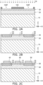
- FIGS. 2A to 3C are schematic cross-sectional views showing manufacturing processes of the semiconductor device 1 according to the embodiment.
- a wafer is prepared in which the first semiconductor layer 20 and the second semiconductor layer 30 are stacked on the semiconductor substrate 10; and a first-conductivity-type impurity, e.g., silicon, is ion-implanted into the front side of the second semiconductor layer 30.
- a first-conductivity-type impurity e.g., silicon
- the semiconductor substrate 10 is, for example, a SiC substrate.
- the semiconductor substrate 10 is, for example, a high-resistance substrate or a semi-insulating substrate.
- the first semiconductor layer 20 and the second semiconductor layer 30 are epitaxially grown on the semiconductor substrate 10 by using MOCVD (Metal Organic Chemical Vapor Deposition).
- the first semiconductor layer 20 is, for example, an n-type GaN layer.
- the first semiconductor layer 20 is, for example, an undoped layer that is not intentionally doped with an impurity.
- the second semiconductor layer 30 is, for example, an n-type AlGaN layer.
- the second semiconductor layer 30 is doped with silicon, which is an n-type impurity, in the epitaxial growth.
- the first semiconductor layer 20 has a higher resistance than the second semiconductor layer 30.
- the first-conductivity-type impurity that is ion-implanted into the front side of the second semiconductor layer 30 is selectively implanted using an ion implantation mask 103 having an opening 103F.
- the ion implantation conditions of the silicon are appropriately set with a dose in the range of 1 ⁇ 10 15 to 1 ⁇ 10 16 cm -2 and an implantation energy in the range of 30 to 100 keV.
- the first-conductivity-type impurity is implanted to have a distribution straddling from the second semiconductor layer 30 into a portion of the first semiconductor layer 20.
- the first region 21, the second region 23, and the third region 25 are formed in the first semiconductor layer 20 by activating the ion-implanted first-conductivity-type impurity. Also, the first region 31, the second region 33, and the third region 35 are formed in the second semiconductor layer 30. After the ion implantation mask 103 is removed, the first-conductivity-type impurity is activated by, for example, heat treatment.
- the first region 21 of the first semiconductor layer 20 is provided between the second region 23 and the third region 25.
- the first-conductivity-type impurity is not ion-implanted into the first region 21.
- the second region 23 and the third region 25 include first-conductivity-type impurities with higher concentrations than the first-conductivity-type impurity of the first region 21.
- the first region 31 of the second semiconductor layer 30 is provided between the second region 33 and the third region 35.
- the first-conductivity-type impurity is not ion-implanted into the first region 31.
- the second region 33 and the third region 35 include first-conductivity-type impurities with higher concentrations than the first-conductivity-type impurity of the first region 31.
- the first electrode 40 is formed on the first region 33 of the second semiconductor layer 30; and the second electrode 50 is formed on the second region 35. Furthermore, the third electrode 60 is formed on the first region 31 of the second semiconductor layer 30.
- the first electrode 40, the second electrode 50, and the third electrode 60 are formed using sputtering.
- the first electrode 40, the second electrode 50, and the third electrode 60 are selectively formed using lift-off.
- the first electrode 40 and the second electrode 50 are, for example, metal layers that include gold and chrome.
- the third electrode 60 is, for example, a metal layer that includes titanium and gold.
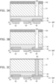
- a via hole VH is formed in the backside of the semiconductor substrate 10.
- the semiconductor substrate 10 is thinned to a prescribed thickness by polishing the backside.
- the via hole VH is formed by selectively removing the semiconductor substrate 10 by using an etching mask 105.
- the etching mask 105 is, for example, a silicon oxide film.
- the via hole VH is formed using inductively coupled plasma dry etching.
- the semiconductor substrate 10 is a SiC substrate
- the semiconductor substrate 10 is etched using an etching gas including fluorine.
- the via hole VH is formed to a depth that extends through the semiconductor substrate 10 and reaches the first semiconductor layer 20.
- the via hole VH is formed to be deeper by selectively removing the first semiconductor layer 20.
- the etching is continued using an etching gas including chlorine (Cl).
- the etching of the semiconductor substrate 10 is stopped and the etching gas is switched at the timing at which the endpoint detector of the dry etching detects gallium (Ga).
- the via hole VH is formed to have a depth that reaches the second semiconductor layer 30.
- the second semiconductor layer 30 is an AlGaN layer, for example, the etching is stopped at the timing at which aluminum (Al) is detected by the endpoint detector.
- connection conductor 80 is formed inside the via hole VH, after which the metal layer 70 is formed on the back surface of the semiconductor substrate 10.
- the connection conductor 80 is formed using plating.
- the connection conductor 80 is, for example, a columnar metal that includes gold.
- the metal layer 70 is formed using sputtering.
- the metal layer 70 includes, for example, nickel and gold.
- connection conductor 80 is formed to contact the second region 33 of the second semiconductor layer 30 and to be electrically connected to the second region 33.
- the second region 33 is positioned between the first electrode 40 and the connection conductor 80.
- the process of forming the via hole VH avoids the exposure of the first electrode 40 at the bottom surface of the via hole VH.
- the first electrode 40 can be prevented from being etched, and the adhesion of residue inside the etching apparatus can be prevented.
- the cleaning frequency of the etching apparatus can be reduced, and the manufacturing efficiency can be increased.
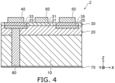
- FIG. 4 is a schematic cross-sectional view showing a semiconductor device 2 according to a modification of the embodiment.
- the connection conductor 80 contacts the second region 23 of the first semiconductor layer 20 and is electrically connected to the second region 23.
- the second region 23 of the first semiconductor layer 20 and the second region 33 of the second semiconductor layer 30 are provided between the first electrode 40 and the connection conductor 80.
- the connection conductor 80 is electrically connected to the first electrode 40 via the second region 23 of the first semiconductor layer 20 and the second region 33 of the second semiconductor layer 30.
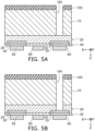
- FIGS. 5A and 5B are schematic cross-sectional views showing manufacturing processes of the semiconductor device 2.
- FIG. 5A illustrates a process corresponding to FIG. 3A .
- the first semiconductor layer 20 is selectively removed after forming the via hole VH to a depth that extends through the semiconductor substrate 10 and reaches the first semiconductor layer 20.
- the via hole VH is formed to a depth that reaches the second region 23 of the first semiconductor layer 20.
- dry etching of the first semiconductor layer 20 is performed using an etching gas including chlorine.
- the end point of the etching is controlled by the etching time.
- the etching of the semiconductor substrate 10 is stopped at the timing at which gallium is detected by the endpoint detector of the dry etching (see FIG. 5A ). Subsequently, the etching gas is switched, and etching of the first semiconductor layer 20 is started. Continuing, the etching is stopped at the timing at which the etching time of the first semiconductor layer 20 reaches a prescribed time.
- connection conductor 80 is formed inside the via hole VH; and the metal layer 70 is formed on the back surface of the semiconductor substrate 10 (see FIG. 3C ).
- FIGS. 6A and 6B are schematic views showing a semiconductor device 3 according to another modification of the embodiment.
- FIG. 6A is a schematic plan view illustrating the upper surface of the semiconductor device 3.
- FIG. 6B is a schematic cross-sectional view along line A-A shown in FIG. 6A .
- the first electrode 40 includes multiple finger parts 40F and a bonding pad part 40P.
- the multiple finger parts 40F are provided to extend in the Y-direction and to be linked to the bonding pad part 40P.
- the second electrode 50 includes multiple finger parts 50F and a bonding pad part 50P.
- the multiple finger parts 50F extend in the Y-direction from the bonding pad part 50P.
- the multiple finger parts 50F are provided to be linked to the bonding pad part 50P.
- the finger part 40F of the first electrode 40 and the finger part 50F of the second electrode 50 are alternately arranged in the X-direction.
- the finger part 40F is provided on the second region 33 of the second semiconductor layer 30; and the finger part 50F is provided on the third region 35 of the second semiconductor layer 30 (see FIG. 1 ).
- the third electrode 60 includes multiple finger parts 60F, a wiring part 60L, and a bonding pad part 60P.
- Each finger part 60F extends in the Y-direction between the finger part 40F of the first electrode 40 and the finger part 50F of the second electrode 50.
- the finger part 60F is provided on the first region 31 of the second semiconductor layer 30 (see FIG. 1 ).
- the wiring part 60L extends in the X-direction; and the finger part 60F is linked to the wiring part 60L.
- the wiring part 60L is linked to the bonding pad part 60P.
- the first semiconductor layer 20 further includes a fourth region 27; and the second semiconductor layer 30 further includes a fourth region 37.
- the fourth region 27 of the first semiconductor layer 20 and the fourth region 37 of the second semiconductor layer 30 are provided between the semiconductor substrate 10 and the bonding pad part 40P of the second electrode 40.
- the first semiconductor layer 20 includes a portion positioned between the semiconductor substrate 10 and the fourth region 27.
- the fourth region 27 of the first semiconductor layer 20 includes a first-conductivity-type impurity with a higher concentration than the first-conductivity-type impurity of the first region 21. Also, the fourth region 37 of the second semiconductor layer 30 includes a first-conductivity-type impurity with a higher concentration than the first-conductivity-type impurity of the first region 31.
- connection conductor 80 extends inside the semiconductor substrate 10 and the first semiconductor layer 20 and is electrically connected to the fourth region 27 of the first semiconductor layer 20 and the fourth region 37 of the second semiconductor layer 30.
- the fourth region 37 of the second semiconductor layer 30 is positioned between the connection conductor 80 and the bonding pad part 40P of the second electrode 40.
- the connection conductor 80 is electrically connected to the bonding pad part 40P of the second electrode 40 via the fourth region 37.
- the first region 21 of the first semiconductor layer 20 also is provided between the third region 25 and the fourth region 27. Also, the first region 31 of the second semiconductor layer 30 is provided between the third region 35 and the fourth region 37.
- the wiring part 60L of the third electrode 60 is provided on the first region 31 of the second semiconductor layer 30.
- the wiring part 60L depletes the first region 21 of the first semiconductor layer 20 between the third region 25 and the fourth region 27 and the first region 31 of the second semiconductor layer 30 between the third region 35 and the fourth region 37. Leakage current between the bonding pad part 40P of the first electrode 40 and the finger part 50F of the second electrode can be blocked thereby.
- the wiring part 60L of the third electrode 60 is electrically insulated from the bonding pad part 40P of the first electrode 40 by an insulating film 65.
- the insulating film 65 is provided between the bonding pad part 40P of the first electrode 40 and the wiring part 60L of the third electrode 60 and covers the wiring part 60L.
- the insulating film 65 is, for example, a silicon oxide film.
- the second region 25 of the first semiconductor layer 20 and the second region 35 of the second semiconductor layer 30 are not provided under the bonding pad part 50P of the second electrode 50 in the example shown in FIG. 6B , the second region 25 and the second region 35 may be provided under the bonding pad part 50P.
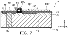
- FIG. 7 is a schematic view showing a semiconductor device 4 according to another modification of the embodiment.
- FIG. 7 illustrates a cross section corresponding to FIG. 6B of the semiconductor device 4.
- an insulating film 67 is provided between the third region 25 and the fourth region 27 of the first semiconductor layer 20 and between the third region 35 and the fourth region 37 of the second semiconductor layer 30.
- the insulating film 67 blocks a leakage current between the bonding pad part 40P of the first electrode 40 and the finger part 50F of the second electrode.
- the insulating film 67 is provided inside a trench formed in the first region 21 between the third region 25 and the fourth region 27 of the first semiconductor layer 20 and in the first region 31 between the third region 35 and the fourth region 37 of the second semiconductor layer 30.
- the insulating film 67 is, for example, a silicon oxide film.
- the wiring part 60L of the third electrode 60 is provided on the insulating film 67.
- FIGS. 8A and 8B are schematic views showing another semiconductor device 5 according to the embodiment.
- FIG. 8A is a plan view showing a capacitor 90.
- FIG. 8B is a schematic cross-sectional view showing the semiconductor device 5 that includes the capacitor 90 on the second semiconductor layer 30.
- the capacitor 90 includes a first metal electrode 93, a dielectric film 95, and a second metal electrode 97.
- the first metal electrode 93, the dielectric film 95, and the second metal electrode 97 are stacked in the Z-direction; and the dielectric film 95 is provided between the first metal electrode 93 and the second metal electrode 97.
- the first metal electrode 93 and the second metal electrode 97 include, for example, gold and chrome.
- the dielectric film 95 includes, for example, a high dielectric constant material such as aluminum oxide, hafnium oxide, etc.
- the capacitor 90 is provided on the second semiconductor layer 30.
- the first metal electrode 93 of the capacitor 90 contacts the second semiconductor layer 30.
- the capacitor 90 is included with the semiconductor device 1 shown in FIG. 1 in, for example, a MMIC (Monolithic Microwave Integrated Circuit).
- the first semiconductor layer 20 further includes a fifth region 29.
- the fifth region 29 is provided between the semiconductor substrate 10 and the first metal electrode 93.
- the second semiconductor layer 20 includes a portion positioned between the semiconductor substrate 10 and the fifth region 29.
- the fifth region 29 includes a first-conductivity-type impurity with a higher concentration than the first-conductivity-type impurity of the first region 21.
- the second semiconductor layer 30 further includes a fifth region 39.
- the fifth region 39 is provided between the first metal electrode 93 and the fifth region 29 of the first semiconductor layer 20.
- the fifth region 39 includes a first-conductivity-type impurity with a higher concentration than the first-conductivity-type impurity of the first region 31.
- the semiconductor device 5 further includes another connection conductor 80.
- the connection conductor 80 is provided to extend inside the semiconductor substrate 10 and the first semiconductor layer 20 and to contact the fifth region 29 of the first semiconductor layer 20 or the fifth region 29 and the fifth region 39 of the second semiconductor layer 30.
- the connection conductor 80 is electrically connected to the first metal electrode 93 via the fifth region 29 of the first semiconductor layer 20 and the fifth region 39 of the second semiconductor layer 30.
- the fifth region 39 of the second semiconductor layer 30 is positioned between the connection conductor 80 and the first metal electrode 93.
- the first metal electrode 93 is electrically connected to the metal layer 70 on the back surface of the semiconductor substrate 10 via at least the connection conductor 80 and the fifth region 39 of the second semiconductor layer 30.
Landscapes
- Junction Field-Effect Transistors (AREA)
- Engineering & Computer Science (AREA)
- Manufacturing & Machinery (AREA)
- Electrodes Of Semiconductors (AREA)
- Internal Circuitry In Semiconductor Integrated Circuit Devices (AREA)
Abstract
Description
- An embodiment relates to a semiconductor device.
- In a semiconductor device in which a semiconductor element such as a transistor or the like is provided at the front side of a semiconductor substrate, there are cases where the semiconductor element and an electrode on the back surface of the semiconductor substrate are electrically connected by forming a via hole from the backside to the semiconductor element.
- [Patent Document 1]
JP 2012-28442 A - [Non-Patent Document 1]
IEICE Technical Report, ED, Electron - An embodiment provides a semiconductor device in which the manufacturing efficiency can be increased.
- A semiconductor device according to an embodiment includes a semiconductor substrate, a first semiconductor layer provided on the semiconductor substrate, a second semiconductor layer provided on the first semiconductor layer, a first electrode provided on the second semiconductor layer, a second electrode provided to be arranged with the first electrode along a front surface of the second semiconductor layer, a third electrode provided between the first electrode and the second electrode on the second semiconductor layer, a metal layer provided on a back surface of the semiconductor substrate at a side opposite to the first semiconductor layer, and a conductor that extends inside the semiconductor substrate and electrically connects the first electrode and the metal layer via the second semiconductor layer. The second semiconductor layer includes a first region including a first-conductivity-type impurity, and a second region including a first-conductivity-type impurity with a higher concentration than the first-conductivity-type impurity of the first region; and the second region of the second semiconductor layer is provided between the conductor and the first electrode.
-
- [
FIG. 1 ]
FIG. 1 is a schematic cross-sectional view showing a semiconductor device according to an embodiment. - [
FIG. 2 ]
FIG. 2 are schematic cross-sectional views showing manufacturing processes of the semiconductor device according to the embodiment. - [
FIG. 3 ]
FIG. 3 are schematic cross-sectional views showing manufacturing processes continuing fromFIG. 2 . - [
FIG. 4 ]
FIG. 4 is a schematic cross-sectional view showing a semiconductor device according to a modification of the embodiment. - [
FIG. 5 ]
FIG. 5 are schematic cross-sectional views showing manufacturing processes of the semiconductor device according to the modification of the embodiment. - [
FIG. 6 ]
FIG. 6 are schematic views showing a semiconductor device according to another modification of the embodiment. - [
FIG. 7 ]
FIG. 7 is a schematic cross-sectional view showing a semiconductor device according to yet another modification of the embodiment. - [
FIG. 8 ]
FIG. 8 are schematic views showing another semiconductor device according to the embodiment. - Embodiments will now be described with reference to the drawings. The same portions in the drawings are marked with the same numerals; a detailed description is omitted as appropriate; and different portions are described. The drawings are schematic or conceptual; and the relationships between the thickness and width of portions, the proportions of sizes among portions, etc., are not necessarily the same as the actual values. Also, the dimensions and proportions may be illustrated differently among drawings, even when the same portion is illustrated.
- Furthermore, the arrangements and configurations of the portions are described using an X-axis, a Y-axis, and a Z-axis shown in the drawings. The X-axis, the Y-axis, and the Z-axis are orthogonal to each other and respectively represent an X-direction, a Y-direction, and a Z-direction. Also, there are cases where the Z-direction is described as up, and the opposite direction is described as down.
-
FIG. 1 is a schematic cross-sectional view showing asemiconductor device 1 according to an embodiment. Thesemiconductor device 1 is, for example, a field-effect transistor (FET). Thesemiconductor device 1 includes asemiconductor substrate 10, afirst semiconductor layer 20, asecond semiconductor layer 30, afirst electrode 40, asecond electrode 50, and athird electrode 60. - The
first semiconductor layer 20 is provided on thesemiconductor substrate 10. Thesecond semiconductor layer 30 is provided on thefirst semiconductor layer 20. Thesemiconductor substrate 10 is, for example, a high-resistance substrate or a semi-insulating substrate. Thesemiconductor substrate 10 is, for example, a silicon carbide (SiC) substrate. Thefirst semiconductor layer 20 is, for example, an n-type gallium nitride (GaN) layer. For example, the bandgap of thesecond semiconductor layer 30 is wider than the bandgap of thefirst semiconductor layer 20. Thesecond semiconductor layer 30 includes, for example, a mixed crystal of the compositional formula Al1-x Ga x N (hereinbelow, AlGaN). Thefirst semiconductor layer 20 and thesecond semiconductor layer 30 each include a first-conductivity-type impurity (hereinbelow, an n-type impurity). - The
first semiconductor layer 20 includes afirst region 21, asecond region 23, and athird region 25. Thesecond region 23 and thethird region 25 each include, for example, an n-type impurity with a higher concentration than the n-type impurity of thefirst region 21. For example, thefirst region 21 is provided between thesecond region 23 and thethird region 25. - The
second semiconductor layer 30 includes afirst region 31, asecond region 33, and athird region 35. For example, thesecond region 33 and thethird region 35 each include an n-type impurity with a higher concentration than the n-type impurity of thefirst region 31. For example, thefirst region 31 is provided between thesecond region 33 and thethird region 35. - The
second region 33 of thesecond semiconductor layer 30 is provided between thefirst electrode 40 and thesecond region 23 of thefirst semiconductor layer 20. Thesecond region 35 of thesecond semiconductor layer 30 is provided between thesecond electrode 50 and thethird region 25 of thefirst semiconductor layer 20. For example, thefirst region 31 of thesecond semiconductor layer 30 is provided between thethird electrode 60 and thefirst region 21 of thefirst semiconductor layer 20. - The
first semiconductor layer 20 includes, for example, a portion extending between thesemiconductor substrate 10 and thesecond region 23. Also, thefirst semiconductor layer 20 includes, for example, a portion extending between thesemiconductor substrate 10 and thethird region 25. - The
first electrode 40, thesecond electrode 50, and thethird electrode 60 are provided on thesecond semiconductor layer 30. Thefirst electrode 40, thesecond electrode 50, and thethird electrode 60 are arranged along the front surface of thesecond semiconductor layer 30. Thethird electrode 60 is provided between thefirst electrode 40 and thesecond electrode 50. - The
first electrode 40 is, for example, a source electrode. Thefirst electrode 40 is electrically connected to thesecond region 33 of thesecond semiconductor layer 30. For example, thefirst electrode 40 has an ohmic contact with thesecond region 33 of thesecond semiconductor layer 30. - The
second electrode 50 is, for example, a drain electrode. Thesecond electrode 50 is electrically connected to thethird region 35 of thesecond semiconductor layer 30. For example, thesecond electrode 50 has an ohmic contact with thesecond region 35 of thesecond semiconductor layer 30. - The
third electrode 60 is, for example, a gate electrode. For example, thethird electrode 60 has a Schottky contact with thefirst region 31 of thesecond semiconductor layer 30. - The
semiconductor device 1 further includes ametal layer 70 and aconnection conductor 80. For example, themetal layer 70 is provided on the back surface of thesemiconductor substrate 10 at the side opposite to thefirst semiconductor layer 20. In other words, thesemiconductor substrate 10 is positioned between thefirst semiconductor layer 20 and themetal layer 70. - The
connection conductor 80 is provided inside thesemiconductor substrate 10 and thefirst semiconductor layer 20. For example, theconnection conductor 80 extends in the direction (e.g., the Z-direction) from themetal layer 70 toward thefirst electrode 40. Theconnection conductor 80 electrically connects themetal layer 70 and thefirst electrode 40. For example, theconnection conductor 80 is electrically connected to thefirst electrode 40 via thesecond region 33 of thesecond semiconductor layer 30. For example, theconnection conductor 80 is provided to contact thesecond region 33. - A method for manufacturing the
semiconductor device 1 will now be described with reference toFIGS. 2A to 3C. FIGS. 2A to 3C are schematic cross-sectional views showing manufacturing processes of thesemiconductor device 1 according to the embodiment. - As shown in
FIG. 2A , a wafer is prepared in which thefirst semiconductor layer 20 and thesecond semiconductor layer 30 are stacked on thesemiconductor substrate 10; and a first-conductivity-type impurity, e.g., silicon, is ion-implanted into the front side of thesecond semiconductor layer 30. - The
semiconductor substrate 10 is, for example, a SiC substrate. Thesemiconductor substrate 10 is, for example, a high-resistance substrate or a semi-insulating substrate. For example, thefirst semiconductor layer 20 and thesecond semiconductor layer 30 are epitaxially grown on thesemiconductor substrate 10 by using MOCVD (Metal Organic Chemical Vapor Deposition). Thefirst semiconductor layer 20 is, for example, an n-type GaN layer. Thefirst semiconductor layer 20 is, for example, an undoped layer that is not intentionally doped with an impurity. Thesecond semiconductor layer 30 is, for example, an n-type AlGaN layer. For example, thesecond semiconductor layer 30 is doped with silicon, which is an n-type impurity, in the epitaxial growth. For example, thefirst semiconductor layer 20 has a higher resistance than thesecond semiconductor layer 30. - For example, the first-conductivity-type impurity that is ion-implanted into the front side of the
second semiconductor layer 30 is selectively implanted using anion implantation mask 103 having anopening 103F. For example, the ion implantation conditions of the silicon are appropriately set with a dose in the range of 1×10¹⁵ to 1×1016 cm-2 and an implantation energy in the range of 30 to 100 keV. For example, the first-conductivity-type impurity is implanted to have a distribution straddling from thesecond semiconductor layer 30 into a portion of thefirst semiconductor layer 20. - As shown in
FIG. 2B , thefirst region 21, thesecond region 23, and thethird region 25 are formed in thefirst semiconductor layer 20 by activating the ion-implanted first-conductivity-type impurity. Also, thefirst region 31, thesecond region 33, and thethird region 35 are formed in thesecond semiconductor layer 30. After theion implantation mask 103 is removed, the first-conductivity-type impurity is activated by, for example, heat treatment. - For example, the
first region 21 of thefirst semiconductor layer 20 is provided between thesecond region 23 and thethird region 25. The first-conductivity-type impurity is not ion-implanted into thefirst region 21. Thesecond region 23 and thethird region 25 include first-conductivity-type impurities with higher concentrations than the first-conductivity-type impurity of thefirst region 21. - The
first region 31 of thesecond semiconductor layer 30 is provided between thesecond region 33 and thethird region 35. The first-conductivity-type impurity is not ion-implanted into thefirst region 31. Thesecond region 33 and thethird region 35 include first-conductivity-type impurities with higher concentrations than the first-conductivity-type impurity of thefirst region 31. - As shown in
FIG. 2C , thefirst electrode 40 is formed on thefirst region 33 of thesecond semiconductor layer 30; and thesecond electrode 50 is formed on thesecond region 35. Furthermore, thethird electrode 60 is formed on thefirst region 31 of thesecond semiconductor layer 30. - For example, the
first electrode 40, thesecond electrode 50, and thethird electrode 60 are formed using sputtering. For example, thefirst electrode 40, thesecond electrode 50, and thethird electrode 60 are selectively formed using lift-off. Thefirst electrode 40 and thesecond electrode 50 are, for example, metal layers that include gold and chrome. Thethird electrode 60 is, for example, a metal layer that includes titanium and gold. - As shown in
FIG. 3A , a via hole VH is formed in the backside of thesemiconductor substrate 10. For example, thesemiconductor substrate 10 is thinned to a prescribed thickness by polishing the backside. Subsequently, for example, the via hole VH is formed by selectively removing thesemiconductor substrate 10 by using anetching mask 105. Theetching mask 105 is, for example, a silicon oxide film. - For example, the via hole VH is formed using inductively coupled plasma dry etching. When the
semiconductor substrate 10 is a SiC substrate, thesemiconductor substrate 10 is etched using an etching gas including fluorine. The via hole VH is formed to a depth that extends through thesemiconductor substrate 10 and reaches thefirst semiconductor layer 20. - As shown in
FIG. 3B , the via hole VH is formed to be deeper by selectively removing thefirst semiconductor layer 20. When thefirst semiconductor layer 20 is a GaN layer, for example, the etching is continued using an etching gas including chlorine (Cl). For example, the etching of thesemiconductor substrate 10 is stopped and the etching gas is switched at the timing at which the endpoint detector of the dry etching detects gallium (Ga). - For example, the via hole VH is formed to have a depth that reaches the
second semiconductor layer 30. When thesecond semiconductor layer 30 is an AlGaN layer, for example, the etching is stopped at the timing at which aluminum (Al) is detected by the endpoint detector. - As shown in
FIG. 3C , theconnection conductor 80 is formed inside the via hole VH, after which themetal layer 70 is formed on the back surface of thesemiconductor substrate 10. For example, theconnection conductor 80 is formed using plating. Theconnection conductor 80 is, for example, a columnar metal that includes gold. For example, themetal layer 70 is formed using sputtering. Themetal layer 70 includes, for example, nickel and gold. - The
connection conductor 80 is formed to contact thesecond region 33 of thesecond semiconductor layer 30 and to be electrically connected to thesecond region 33. Thesecond region 33 is positioned between thefirst electrode 40 and theconnection conductor 80. - According to the embodiment, the process of forming the via hole VH avoids the exposure of the
first electrode 40 at the bottom surface of the via hole VH. Thereby, thefirst electrode 40 can be prevented from being etched, and the adhesion of residue inside the etching apparatus can be prevented. As a result, the cleaning frequency of the etching apparatus can be reduced, and the manufacturing efficiency can be increased. -
FIG. 4 is a schematic cross-sectional view showing asemiconductor device 2 according to a modification of the embodiment. In thesemiconductor device 2, theconnection conductor 80 contacts thesecond region 23 of thefirst semiconductor layer 20 and is electrically connected to thesecond region 23. Thesecond region 23 of thefirst semiconductor layer 20 and thesecond region 33 of thesecond semiconductor layer 30 are provided between thefirst electrode 40 and theconnection conductor 80. Theconnection conductor 80 is electrically connected to thefirst electrode 40 via thesecond region 23 of thefirst semiconductor layer 20 and thesecond region 33 of thesecond semiconductor layer 30. -
FIGS. 5A and 5B are schematic cross-sectional views showing manufacturing processes of thesemiconductor device 2.FIG. 5A illustrates a process corresponding toFIG. 3A . - As shown in
FIG. 5A , thefirst semiconductor layer 20 is selectively removed after forming the via hole VH to a depth that extends through thesemiconductor substrate 10 and reaches thefirst semiconductor layer 20. - As shown in
FIG. 5B , the via hole VH is formed to a depth that reaches thesecond region 23 of thefirst semiconductor layer 20. For example, dry etching of thefirst semiconductor layer 20 is performed using an etching gas including chlorine. For example, the end point of the etching is controlled by the etching time. - When the
first semiconductor layer 20 is a GaN layer, for example, the etching of thesemiconductor substrate 10 is stopped at the timing at which gallium is detected by the endpoint detector of the dry etching (seeFIG. 5A ). Subsequently, the etching gas is switched, and etching of thefirst semiconductor layer 20 is started. Continuing, the etching is stopped at the timing at which the etching time of thefirst semiconductor layer 20 reaches a prescribed time. - Continuing, the
connection conductor 80 is formed inside the via hole VH; and themetal layer 70 is formed on the back surface of the semiconductor substrate 10 (seeFIG. 3C ). -
FIGS. 6A and 6B are schematic views showing asemiconductor device 3 according to another modification of the embodiment.FIG. 6A is a schematic plan view illustrating the upper surface of thesemiconductor device 3.FIG. 6B is a schematic cross-sectional view along line A-A shown inFIG. 6A . - As shown in
FIG. 6A , thefirst electrode 40 includesmultiple finger parts 40F and abonding pad part 40P. For example, themultiple finger parts 40F are provided to extend in the Y-direction and to be linked to thebonding pad part 40P. - The
second electrode 50 includesmultiple finger parts 50F and abonding pad part 50P. For example, themultiple finger parts 50F extend in the Y-direction from thebonding pad part 50P. Themultiple finger parts 50F are provided to be linked to thebonding pad part 50P. - For example, the
finger part 40F of thefirst electrode 40 and thefinger part 50F of thesecond electrode 50 are alternately arranged in the X-direction. Thefinger part 40F is provided on thesecond region 33 of thesecond semiconductor layer 30; and thefinger part 50F is provided on thethird region 35 of the second semiconductor layer 30 (seeFIG. 1 ). - The
third electrode 60 includesmultiple finger parts 60F, awiring part 60L, and abonding pad part 60P. Eachfinger part 60F extends in the Y-direction between thefinger part 40F of thefirst electrode 40 and thefinger part 50F of thesecond electrode 50. Thefinger part 60F is provided on thefirst region 31 of the second semiconductor layer 30 (seeFIG. 1 ). Thewiring part 60L extends in the X-direction; and thefinger part 60F is linked to thewiring part 60L. Thewiring part 60L is linked to thebonding pad part 60P. - As shown in
FIG. 6B , thefirst semiconductor layer 20 further includes afourth region 27; and thesecond semiconductor layer 30 further includes afourth region 37. Thefourth region 27 of thefirst semiconductor layer 20 and thefourth region 37 of thesecond semiconductor layer 30 are provided between thesemiconductor substrate 10 and thebonding pad part 40P of thesecond electrode 40. Thefirst semiconductor layer 20 includes a portion positioned between thesemiconductor substrate 10 and thefourth region 27. - The
fourth region 27 of thefirst semiconductor layer 20 includes a first-conductivity-type impurity with a higher concentration than the first-conductivity-type impurity of thefirst region 21. Also, thefourth region 37 of thesecond semiconductor layer 30 includes a first-conductivity-type impurity with a higher concentration than the first-conductivity-type impurity of thefirst region 31. - The
connection conductor 80 extends inside thesemiconductor substrate 10 and thefirst semiconductor layer 20 and is electrically connected to thefourth region 27 of thefirst semiconductor layer 20 and thefourth region 37 of thesecond semiconductor layer 30. Thefourth region 37 of thesecond semiconductor layer 30 is positioned between theconnection conductor 80 and thebonding pad part 40P of thesecond electrode 40. Theconnection conductor 80 is electrically connected to thebonding pad part 40P of thesecond electrode 40 via thefourth region 37. - The
first region 21 of thefirst semiconductor layer 20 also is provided between thethird region 25 and thefourth region 27. Also, thefirst region 31 of thesecond semiconductor layer 30 is provided between thethird region 35 and thefourth region 37. - The
wiring part 60L of thethird electrode 60 is provided on thefirst region 31 of thesecond semiconductor layer 30. For example, at turn-off of thesemiconductor device 3, thewiring part 60L depletes thefirst region 21 of thefirst semiconductor layer 20 between thethird region 25 and thefourth region 27 and thefirst region 31 of thesecond semiconductor layer 30 between thethird region 35 and thefourth region 37. Leakage current between thebonding pad part 40P of thefirst electrode 40 and thefinger part 50F of the second electrode can be blocked thereby. - The
wiring part 60L of thethird electrode 60 is electrically insulated from thebonding pad part 40P of thefirst electrode 40 by an insulatingfilm 65. The insulatingfilm 65 is provided between thebonding pad part 40P of thefirst electrode 40 and thewiring part 60L of thethird electrode 60 and covers thewiring part 60L. The insulatingfilm 65 is, for example, a silicon oxide film. - Although the
second region 25 of thefirst semiconductor layer 20 and thesecond region 35 of thesecond semiconductor layer 30 are not provided under thebonding pad part 50P of thesecond electrode 50 in the example shown inFIG. 6B , thesecond region 25 and thesecond region 35 may be provided under thebonding pad part 50P. -
FIG. 7 is a schematic view showing asemiconductor device 4 according to another modification of the embodiment.FIG. 7 illustrates a cross section corresponding toFIG. 6B of thesemiconductor device 4. - In the
semiconductor device 4 as shown inFIG. 7 , an insulatingfilm 67 is provided between thethird region 25 and thefourth region 27 of thefirst semiconductor layer 20 and between thethird region 35 and thefourth region 37 of thesecond semiconductor layer 30. The insulatingfilm 67 blocks a leakage current between thebonding pad part 40P of thefirst electrode 40 and thefinger part 50F of the second electrode. - For example, the insulating
film 67 is provided inside a trench formed in thefirst region 21 between thethird region 25 and thefourth region 27 of thefirst semiconductor layer 20 and in thefirst region 31 between thethird region 35 and thefourth region 37 of thesecond semiconductor layer 30. The insulatingfilm 67 is, for example, a silicon oxide film. Thewiring part 60L of thethird electrode 60 is provided on the insulatingfilm 67. -
FIGS. 8A and 8B are schematic views showing anothersemiconductor device 5 according to the embodiment.FIG. 8A is a plan view showing acapacitor 90.FIG. 8B is a schematic cross-sectional view showing thesemiconductor device 5 that includes thecapacitor 90 on thesecond semiconductor layer 30. - As shown in
FIG. 8A , thecapacitor 90 includes afirst metal electrode 93, adielectric film 95, and asecond metal electrode 97. For example, thefirst metal electrode 93, thedielectric film 95, and thesecond metal electrode 97 are stacked in the Z-direction; and thedielectric film 95 is provided between thefirst metal electrode 93 and thesecond metal electrode 97. Thefirst metal electrode 93 and thesecond metal electrode 97 include, for example, gold and chrome. Thedielectric film 95 includes, for example, a high dielectric constant material such as aluminum oxide, hafnium oxide, etc. - As shown in
FIG. 8B , thecapacitor 90 is provided on thesecond semiconductor layer 30. For example, thefirst metal electrode 93 of thecapacitor 90 contacts thesecond semiconductor layer 30. Also, thecapacitor 90 is included with thesemiconductor device 1 shown inFIG. 1 in, for example, a MMIC (Monolithic Microwave Integrated Circuit). - In the example, the
first semiconductor layer 20 further includes afifth region 29. Thefifth region 29 is provided between thesemiconductor substrate 10 and thefirst metal electrode 93. Thesecond semiconductor layer 20 includes a portion positioned between thesemiconductor substrate 10 and thefifth region 29. Thefifth region 29 includes a first-conductivity-type impurity with a higher concentration than the first-conductivity-type impurity of thefirst region 21. - The
second semiconductor layer 30 further includes afifth region 39. Thefifth region 39 is provided between thefirst metal electrode 93 and thefifth region 29 of thefirst semiconductor layer 20. Thefifth region 39 includes a first-conductivity-type impurity with a higher concentration than the first-conductivity-type impurity of thefirst region 31. - The
semiconductor device 5 further includes anotherconnection conductor 80. Theconnection conductor 80 is provided to extend inside thesemiconductor substrate 10 and thefirst semiconductor layer 20 and to contact thefifth region 29 of thefirst semiconductor layer 20 or thefifth region 29 and thefifth region 39 of thesecond semiconductor layer 30. Theconnection conductor 80 is electrically connected to thefirst metal electrode 93 via thefifth region 29 of thefirst semiconductor layer 20 and thefifth region 39 of thesecond semiconductor layer 30. Also, thefifth region 39 of thesecond semiconductor layer 30 is positioned between theconnection conductor 80 and thefirst metal electrode 93. - In the
semiconductor device 5, thefirst metal electrode 93 is electrically connected to themetal layer 70 on the back surface of thesemiconductor substrate 10 via at least theconnection conductor 80 and thefifth region 39 of thesecond semiconductor layer 30. - While certain embodiments of the inventions have been described, these embodiments have been presented by way of example only, and are not intended to limit the scope of the inventions. These novel embodiments may be embodied in a variety of other forms; and various omissions, substitutions, and changes may be made without departing from the spirit of the inventions. Such embodiments and their modifications are within the scope and spirit of the inventions, and are within the scope of the inventions described in the claims and their equivalents.
Claims (9)
- A semiconductor device, comprising:a semiconductor substrate;a first semiconductor layer provided on the semiconductor su bstrate;a second semiconductor layer provided on the first semiconductor layer;a first electrode provided on the second semiconductor layer;a second electrode provided to be arranged with the first electrode along a front surface of the second semiconductor layer;a third electrode provided between the first electrode and the second electrode on the second semiconductor layer;a metal layer provided on a back surface of the semiconductor substrate at a side opposite to the first semiconductor layer; anda conductor extending inside the semiconductor substrate,the conductor electrically connecting the first electrode and the metal layer via the second semiconductor layer,the second semiconductor layer includinga first region including a first-conductivity-type impurity, anda second region including a first-conductivity-type impurity with a higher concentration than the first-conductivity-type impurity of the first region,the second region of the second semiconductor layer being provided between the conductor and the first electrode.
- The semiconductor device according to claim 1 or 2, whereinthe first semiconductor layer includes:a first region including a first-conductivity-type impurity; anda second region including a first-conductivity-type impurity with a higher concentration than the first-conductivity-type impurity of the first region, andthe second region of the second semiconductor layer is provided between the first electrode and the second region of the first semiconductor layer.
- The semiconductor device according to claim 2, wherein
the conductor contacts the second region of the second semiconductor layer. - The semiconductor device according to claim 2, wherein
the conductor contacts the second region of the first semiconductor layer. - The semiconductor device according to any one of claims 2 to 4, wherein
the second region of the first semiconductor layer contacts the second region of the second semiconductor layer. - The semiconductor device according to any one of claims 2 to 5, whereinthe second semiconductor layer further includes a third region provided between the second electrode and the first semiconductor layer, andthe third region includes a first-conductivity-type impurity with a higher concentration than the first-conductivity-type impurity of the first region of the second semiconductor layer.
- The semiconductor device according to claim 6, whereinthe first semiconductor layer further includes a third region,the third region includes a first-conductivity-type impurity,the third region of the second semiconductor layer is provided between the second electrode and the third region of the first semiconductor layer, andthe third region of the first semiconductor layer includes the first-conductivity-type impurity with a higher concentration than the first-conductivity-type impurity of the first region of the first semiconductor layer.
- The semiconductor device according to any one of claims 1 to 7, wherein
a bandgap of the second semiconductor layer is wider than a bandgap of the first semiconductor layer. - The semiconductor device according to any one of claims 1 to 8, wherein
the first semiconductor layer has a higher resistance than the second semiconductor layer.
Applications Claiming Priority (2)
| Application Number | Priority Date | Filing Date | Title |
|---|---|---|---|
| JP2020129238A JP2022025995A (en) | 2020-07-30 | 2020-07-30 | Semiconductor device |
| PCT/JP2021/027568 WO2022025000A1 (en) | 2020-07-30 | 2021-07-26 | Semiconductor device |
Publications (2)
| Publication Number | Publication Date |
|---|---|
| EP4191684A1 true EP4191684A1 (en) | 2023-06-07 |
| EP4191684A4 EP4191684A4 (en) | 2024-10-23 |
Family
ID=80036457
Family Applications (1)
| Application Number | Title | Priority Date | Filing Date |
|---|---|---|---|
| EP21850141.9A Pending EP4191684A4 (en) | 2020-07-30 | 2021-07-26 | SEMICONDUCTOR DEVICE |
Country Status (4)
| Country | Link |
|---|---|
| US (1) | US12439671B2 (en) |
| EP (1) | EP4191684A4 (en) |
| JP (1) | JP2022025995A (en) |
| WO (1) | WO2022025000A1 (en) |
Families Citing this family (1)
| Publication number | Priority date | Publication date | Assignee | Title |
|---|---|---|---|---|
| KR20240030267A (en) * | 2022-08-30 | 2024-03-07 | 삼성전자주식회사 | Plasma sensor module and method of manufacturing the same |
Family Cites Families (14)
| Publication number | Priority date | Publication date | Assignee | Title |
|---|---|---|---|---|
| US9711633B2 (en) | 2008-05-09 | 2017-07-18 | Cree, Inc. | Methods of forming group III-nitride semiconductor devices including implanting ions directly into source and drain regions and annealing to activate the implanted ions |
| JP4687793B2 (en) | 2009-01-14 | 2011-05-25 | トヨタ自動車株式会社 | Exhaust gas recirculation device |
| JP5566803B2 (en) | 2010-07-21 | 2014-08-06 | 住友電工デバイス・イノベーション株式会社 | Manufacturing method of semiconductor device |
| JP2013074068A (en) | 2011-09-27 | 2013-04-22 | Fujitsu Ltd | Semiconductor device and manufacturing method of semiconductor device |
| JP2013098274A (en) * | 2011-10-31 | 2013-05-20 | Toshiba Corp | Semiconductor device |
| JP2013183060A (en) * | 2012-03-02 | 2013-09-12 | Toshiba Corp | Semiconductor device |
| US8748245B1 (en) * | 2013-03-27 | 2014-06-10 | Io Semiconductor, Inc. | Semiconductor-on-insulator integrated circuit with interconnect below the insulator |
| DE102013224361A1 (en) * | 2013-11-28 | 2015-05-28 | Fraunhofer-Gesellschaft zur Förderung der angewandten Forschung e.V. | Field effect transistor and method for its production |
| US9397180B1 (en) * | 2015-04-24 | 2016-07-19 | Texas Instruments Incorporated | Low resistance sinker contact |
| US10256294B2 (en) * | 2015-05-18 | 2019-04-09 | Qorvo Us, Inc. | Vertical gallium nitride power field-effect transistor with a field plate structure |
| JP6552925B2 (en) | 2015-09-04 | 2019-07-31 | 株式会社東芝 | Semiconductor device |
| US10439565B2 (en) * | 2017-09-27 | 2019-10-08 | Qualcomm Incorporated | Low parasitic capacitance low noise amplifier |
| JP7082508B2 (en) * | 2018-03-22 | 2022-06-08 | ローム株式会社 | Nitride semiconductor equipment |
| CN112018175B (en) * | 2019-05-30 | 2022-04-08 | 苏州捷芯威半导体有限公司 | Semiconductor device, preparation method thereof and semiconductor packaging structure |
-
2020
- 2020-07-30 JP JP2020129238A patent/JP2022025995A/en active Pending
-
2021
- 2021-07-26 EP EP21850141.9A patent/EP4191684A4/en active Pending
- 2021-07-26 WO PCT/JP2021/027568 patent/WO2022025000A1/en not_active Ceased
- 2021-07-26 US US18/007,227 patent/US12439671B2/en active Active
Also Published As
| Publication number | Publication date |
|---|---|
| WO2022025000A1 (en) | 2022-02-03 |
| EP4191684A4 (en) | 2024-10-23 |
| US12439671B2 (en) | 2025-10-07 |
| US20230307516A1 (en) | 2023-09-28 |
| JP2022025995A (en) | 2022-02-10 |
Similar Documents
| Publication | Publication Date | Title |
|---|---|---|
| Kim | Lee | |
| EP3413353B1 (en) | Normally-off hemt transistor with selective generation of 2deg channel, and manufacturing method thereof | |
| US20210351288A1 (en) | Semiconductor structure having both enhancement mode group iii-n high electron mobility transistors and depletion mode group iii-n high electron mobility transistors | |
| EP2793255B1 (en) | Manufacturing method of a semiconductor device comprising a schottky diode and a high electron mobility transistor | |
| US8680580B2 (en) | Field effect transistor and process for manufacturing same | |
| EP2601678B1 (en) | Manufacturing of scalable gate length high electron mobility transistors | |
| US20060043416A1 (en) | Recessed semiconductor device | |
| US11222973B2 (en) | Semiconductor device | |
| US10872967B2 (en) | Manufacturing method of semiconductor device | |
| KR20110041550A (en) | Normally-off semiconductor device and manufacturing method thereof | |
| CN111463260A (en) | Vertical high electron mobility field effect transistor and preparation method thereof | |
| US11973135B2 (en) | Semiconductor device | |
| EP3834233A1 (en) | Extrinsic field termination structures for improving reliability of high-voltage, high-power active devices | |
| JP2017157589A (en) | Semiconductor device and semiconductor device manufacturing method | |
| JP2024519853A (en) | III-nitride transistor having back barrier structure and buried p-type layer and method thereof | |
| JP2024528764A (en) | GaN-based HEMT structure having multiple threshold voltages, its manufacturing method and uses | |
| JP5126733B2 (en) | Field effect transistor and manufacturing method thereof | |
| US12439671B2 (en) | Semiconductor device | |
| KR20110105032A (en) | A nitride semiconductor device having a recess gate edge structure and a method of manufacturing the same | |
| KR100770132B1 (en) | Nitride-based semiconductor device | |
| US20240274507A1 (en) | Vias for Semiconductor Devices Formed from Multiple Etching | |
| CN117878150A (en) | A HEMT with integrated GaN diode temperature sensor and its preparation method | |
| US20180182891A1 (en) | Method of manufacturing a semiconductor device | |
| RU2705761C1 (en) | Semiconductor device | |
| KR102829615B1 (en) | Schottky barrier diode and method for manufacturing the same |
Legal Events
| Date | Code | Title | Description |
|---|---|---|---|
| STAA | Information on the status of an ep patent application or granted ep patent |
Free format text: STATUS: THE INTERNATIONAL PUBLICATION HAS BEEN MADE |
|
| PUAI | Public reference made under article 153(3) epc to a published international application that has entered the european phase |
Free format text: ORIGINAL CODE: 0009012 |
|
| STAA | Information on the status of an ep patent application or granted ep patent |
Free format text: STATUS: REQUEST FOR EXAMINATION WAS MADE |
|
| 17P | Request for examination filed |
Effective date: 20230126 |
|
| AK | Designated contracting states |
Kind code of ref document: A1 Designated state(s): AL AT BE BG CH CY CZ DE DK EE ES FI FR GB GR HR HU IE IS IT LI LT LU LV MC MK MT NL NO PL PT RO RS SE SI SK SM TR |
|
| DAV | Request for validation of the european patent (deleted) | ||
| DAX | Request for extension of the european patent (deleted) | ||
| A4 | Supplementary search report drawn up and despatched |
Effective date: 20240923 |
|
| RIC1 | Information provided on ipc code assigned before grant |
Ipc: H01L 29/08 20060101ALN20240917BHEP Ipc: H01L 29/778 20060101ALI20240917BHEP Ipc: H01L 23/522 20060101ALI20240917BHEP Ipc: H01L 21/768 20060101ALI20240917BHEP Ipc: H01L 21/338 20060101ALI20240917BHEP Ipc: H01L 21/3205 20060101ALI20240917BHEP Ipc: H01L 29/812 20060101AFI20240917BHEP |
|
| STAA | Information on the status of an ep patent application or granted ep patent |
Free format text: STATUS: EXAMINATION IS IN PROGRESS |
|
| 17Q | First examination report despatched |
Effective date: 20250709 |
|
| RAP1 | Party data changed (applicant data changed or rights of an application transferred) |
Owner name: KABUSHIKI KAISHA TOSHIBA |