EP4191647A1 - Crack detector for semiconductor dies - Google Patents
Crack detector for semiconductor dies Download PDFInfo
- Publication number
- EP4191647A1 EP4191647A1 EP22207185.4A EP22207185A EP4191647A1 EP 4191647 A1 EP4191647 A1 EP 4191647A1 EP 22207185 A EP22207185 A EP 22207185A EP 4191647 A1 EP4191647 A1 EP 4191647A1
- Authority
- EP
- European Patent Office
- Prior art keywords
- test
- resistive
- signal
- resistive path
- assembly
- Prior art date
- Legal status (The legal status is an assumption and is not a legal conclusion. Google has not performed a legal analysis and makes no representation as to the accuracy of the status listed.)
- Pending
Links
Images




Classifications
-
- G—PHYSICS
- G01—MEASURING; TESTING
- G01N—INVESTIGATING OR ANALYSING MATERIALS BY DETERMINING THEIR CHEMICAL OR PHYSICAL PROPERTIES
- G01N27/00—Investigating or analysing materials by the use of electric, electrochemical, or magnetic means
- G01N27/02—Investigating or analysing materials by the use of electric, electrochemical, or magnetic means by investigating impedance
- G01N27/04—Investigating or analysing materials by the use of electric, electrochemical, or magnetic means by investigating impedance by investigating resistance
- G01N27/20—Investigating the presence of flaws
-
- G—PHYSICS
- G01—MEASURING; TESTING
- G01R—MEASURING ELECTRIC VARIABLES; MEASURING MAGNETIC VARIABLES
- G01R31/00—Arrangements for testing electric properties; Arrangements for locating electric faults; Arrangements for electrical testing characterised by what is being tested not provided for elsewhere
- G01R31/28—Testing of electronic circuits, e.g. by signal tracer
- G01R31/302—Contactless testing
- G01R31/315—Contactless testing by inductive methods
-
- H—ELECTRICITY
- H10—SEMICONDUCTOR DEVICES; ELECTRIC SOLID-STATE DEVICES NOT OTHERWISE PROVIDED FOR
- H10P—GENERIC PROCESSES OR APPARATUS FOR THE MANUFACTURE OR TREATMENT OF DEVICES COVERED BY CLASS H10
- H10P74/00—Testing or measuring during manufacture or treatment of wafers, substrates or devices
- H10P74/27—Structural arrangements therefor
- H10P74/277—Circuits for electrically characterising or monitoring manufacturing processes, e.g. circuits in tested chips or circuits in testing wafers
-
- G—PHYSICS
- G01—MEASURING; TESTING
- G01N—INVESTIGATING OR ANALYSING MATERIALS BY DETERMINING THEIR CHEMICAL OR PHYSICAL PROPERTIES
- G01N27/00—Investigating or analysing materials by the use of electric, electrochemical, or magnetic means
- G01N27/02—Investigating or analysing materials by the use of electric, electrochemical, or magnetic means by investigating impedance
- G01N27/04—Investigating or analysing materials by the use of electric, electrochemical, or magnetic means by investigating impedance by investigating resistance
- G01N27/20—Investigating the presence of flaws
- G01N27/205—Investigating the presence of flaws in insulating materials
-
- H—ELECTRICITY
- H10—SEMICONDUCTOR DEVICES; ELECTRIC SOLID-STATE DEVICES NOT OTHERWISE PROVIDED FOR
- H10P—GENERIC PROCESSES OR APPARATUS FOR THE MANUFACTURE OR TREATMENT OF DEVICES COVERED BY CLASS H10
- H10P74/00—Testing or measuring during manufacture or treatment of wafers, substrates or devices
- H10P74/20—Testing or measuring during manufacture or treatment of wafers, substrates or devices characterised by the properties tested or measured, e.g. structural or electrical properties
- H10P74/203—Structural properties, e.g. testing or measuring thicknesses, line widths, warpage, bond strengths or physical defects
-
- H—ELECTRICITY
- H10—SEMICONDUCTOR DEVICES; ELECTRIC SOLID-STATE DEVICES NOT OTHERWISE PROVIDED FOR
- H10P—GENERIC PROCESSES OR APPARATUS FOR THE MANUFACTURE OR TREATMENT OF DEVICES COVERED BY CLASS H10
- H10P74/00—Testing or measuring during manufacture or treatment of wafers, substrates or devices
- H10P74/20—Testing or measuring during manufacture or treatment of wafers, substrates or devices characterised by the properties tested or measured, e.g. structural or electrical properties
- H10P74/207—Electrical properties, e.g. testing or measuring of resistance, deep levels or capacitance-voltage characteristics
-
- H—ELECTRICITY
- H10—SEMICONDUCTOR DEVICES; ELECTRIC SOLID-STATE DEVICES NOT OTHERWISE PROVIDED FOR
- H10W—GENERIC PACKAGES, INTERCONNECTIONS, CONNECTORS OR OTHER CONSTRUCTIONAL DETAILS OF DEVICES COVERED BY CLASS H10
- H10W42/00—Arrangements for protection of devices
Definitions
- the present invention relates to an assembly for detecting a structural defect in a semiconductor die.
- Wafer singulation process for dice is a sensitive manufacturing step (specifically for LowK and ultra-LowK technologies). To secure this process, it is possible to detect failures linked to chipping and cracks in the seal ring of the dice (during the "Back-end-Of-Line", BEOL, manufacturing phase), using a so-called crack detector.
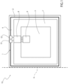
- a die 10 is shown in a top-plan view, and includes a crack sensor, or detector, 1.
- the crack sensor 1 is, in one exemplary embodiment of the known art, formed by several elements:
- the conductive line 2 is substantially a continuous strip of conductive material, having a certain resistance, extending between two electrical nodes E1, E2.
- the conductive line 2 can be formed by one or two sub-lines; in case of two sub-lines, one sub-line is placed between the seal ring area 4 and the I/O ring 7, and is also known as "inner sensor", and the other sub-line is placed within the seal ring area 4 and is also known as "outer sensor”.
- Each sub-line is realized as a via chain (see Figure 2 ). This solution with two sub-lines, or sub-sensors, permits to detect, in addition to cracks, also delamination defects.
- N-well straps may be inserted in the sensors terminals in order not to "break" the metal continuity of the seal ring area 4.
- Measuring the electrical continuity of the sensor 1 during EWS (Electrical Wafer Sorting") and FT (“Final Test”) through the detector cell 8 allows to detect, and screen out, portions of the seal ring having cracks. Affecting a specific bin and SBL to this test will allow a correct monitoring of the defect rate and to take adequate actions in case of need.
- the use of the sensor 1 improves the robustness of the chip product, enables detection of cracks in the BEOL at "time zero", which prevents delivery of weak parts that become failed parts in the customer application (when thermomechanical or humidity constraints play a major role).
- Use of sensor 1 has a negligible impact on test time (it requires to test of a simple resistor), and does not introduce disturbances of functionality for RF products.
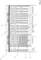
- FIG. 2 shows a cross-sectional view of an embodiment of (a portion of) a crack sensor 1 according to the known art.
- the crack sensor 1 of Figure 2 may be used for chips with an interconnect structure of more than two metal layers.
- Substrate conductive segments 11 are arranged in a substrate 12. A first portion of the substrate conductive segment 11 is connected to a first conductive segment 14 in the M1 metallization level. A second portion of the substrate conductive segment 11 is connected to a second conductive segment 15 in the M1 metallization level.
- the first conductive segment 14 is connected to a plurality of further conductive segments 16 in upper metallization levels through a plurality of interlayer connects.
- the second conductive segment 15 is connected to a plurality of further conductive segments 18 in upper metallization levels through a plurality of respective interlayer connects.
- the interlayer connects may comprise contacts and/or plugs/vias.
- the structure of Figures 1 and 2 may be used to detect cracks that may form when the dies 10 are separated (singulated) from the wafer.
- the crack detector is a resistive sensor composed of a metal wire with two electrical nodes. This metal wire is placed around the die close to seal ring. Measuring the continuity of this wire allows to detect cracks.
- a voltage is applied across the electrical nodes E1, E2.
- a current flows during the application of the voltage to the two nodes E1, E2. If there is no (or almost no) voltage drop over the resistive line 2, the sensor is intact and a crack is not disrupted or broken. If there is some voltage drop over the resistive line 2, the sensor may partially be broken, and if there is a complete or almost complete voltage drop over the resistive line 2, the sensor may be cut or severely damaged.
- a digital testing can also be carried out.
- Figure 3 shows a circuit design for performing digital testing.
- a digital signal DATAIN is set as input to electrical node E1 of the crack sensor 1.
- Signal DATAIN goes from digital value "0" to digital value "1".
- An input buffer stage 20 is provided to receive the signal DATAIN, rectify the signal DATAIN and drive properly the crack sensor 1 through node E1.
- An output buffer stage 21 is provided coupled to output electrical node E2 of the crack sensor 1, to receive the signal that propagates through the crack sensor 1, rectify the signal and provide at output a digital signal SOUT.
- the signal DATAIN is generated by the test logic 9, and the input buffer stage 20 is part of the detector cell 8, analogously, the signal SOUT is received by the test logic 9 and the output buffer stage 21 is part of the detector cell 8.
- the signal SOUT corresponds to the signal DATAIN, and is received with a certain time delay.
- interruptions of the resistive line 2 no signal SOUT is received, or the signal SOUT considerably differs from the signal DATAIN. A crack, or another issue along the resistive line 2, is thus revealed.
- Patent document DE102004028695 relates to a semiconductor component having a semiconductor body which has an edge, a central region and an edge region arranged between the edge and the central region.
- Patent document US 2015/115266 relates generally to semiconductor device fabrication and more specifically to detecting cracks in semiconductor substrates.
- Patent document US 2014/049284 relates to a test device for testing a semiconductor device, a semiconductor device, a semiconductor device and a testing method thereof and more particularly to a test device for testing a semiconductor device, a semiconductor device and a testing method thereof to test whether a TSV (Thru Silicon Via) included in a semiconductor device is formed without defects such as a crack therein and whether the TSV is connected to a metal layer or not.
- TSV Thru Silicon Via
- the aim of the present invention is to overcome the problems previously illustrated.
- an assembly for detecting a structural defect in a semiconductor die is provided, as defined in claim 1.
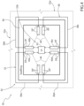
- FIG. 4 shows a die 30 housing a crack-detection sensor 32 (in the following also referred to as “crack sensor”), according to an embodiment of the present invention.
- the die 30 derives from a semiconductor wafer comprising a plurality of dies 30 formed across a top surface of the wafer, after the semiconductor dies have been diced (i.e., cut into individual dies from a wafer).
- the die 30 is typically square or rectangular in shape.
- the die 30 comprises an integrated circuit (not shown in detail).
- the plurality of dies are separated from one another along scribe lines (the so-called "singulation" step).
- the scribe lines are located at the perimeter of the die 30, so that at the end of the manufacturing process a saw can be used to detach one die from adjacent dies along the scribe lines.
- the singulation of the dies may also be performed, for example, by laser dicing or laser scribing followed by saw dicing.
- the crack sensor 32 is formed in at least one conductive-material layer (metal layer) of the die 30, more preferably in a plurality of overlying metal layers separated from one another by dielectric or insulating layers and connected by means of vias passing through such dielectric or insulating layers.
- the crack sensor 32 is, in particular, formed at least in part along a perimeter region 34 of the die 30, as shown in Figure 4 .
- the crack sensor 32 is formed between an edge 32a of the die 32 and an interior region 32b of the die 32, wherein the interior region 32b houses the integrated circuit.
- a seal region, or seal ring, 36 is also present between the edge 32a and the interior region 32b.
- a seal ring is, for example, a multi-layer structure composed of alternating conducting and insulating layers. Through each of the insulating layers run multiple vias which provide electrical paths between adjacent metal layers. The lowest layer of metal in the seal structure makes electrical contact with the substrate, which can be either p-type or n-type.
- the seal ring 36 may be omitted.
- the crack sensor 32 comprises a resistive structure 38 of conductive material having a certain electrical resistance, which extends, or is integrated, proximate the edge 32a, at least in part between (in a top view) the seal ring 36 and the edge 32a.
- the resistive structure 38 comprises a plurality of resistive segments 38a-38d of conductive material having a certain electrical resistance (in the following, also named "conductive segments"), formed in one or more metal layers of the die 30; in other words, the conductive structure is formed in a plurality of metal layers in a multi-level interconnect system, wherein vias are used to connect one metal level to another (analogously to the prior art shown in Figure 2 ).
- Each conductive segment 38a-d comprises a first end 39' and a second end 39".
- each conductive segment 38a-d extends mainly along the edge 32a, the first end 39' and the second end 39" are in the interior region 32b (therefore, at least a portion of the conductive segments 38a-d extends from the edge 32a to the interior region 32b, or viceversa, through the seal ring 36).
- the first end 39' and the second end 39" of each conductive segment 38a-d are coupled to respective end portions of a respective oscillator module 40a-40d; each oscillator module 40a-40d includes elements (in particular, in one embodiment, passive electronic devices) configured for generating an oscillating signals, having an own frequency, throughout the conductive segment 38a-38d. The frequency of the oscillating signals can be used for checking the structural integrity of the die 30.
- the frequencies of the oscillating signals in each conductive segment 38a-38d can be measured and compared with a reference frequency (pre-set value), or compared with one another.
- a reference frequency pre-set value
- the result of the comparison is indicative of the presence of a defect.
- the result of the comparison is indicative of the presence of a defect.
- Computing means such as a microcontroller 43, are present to perform operations aimed at verifying the presence of the structural defect, as better discussed later.
- the microcontroller 43 can be integrated in the semiconductor die 30 (in the region 32b), or arranged external to the semiconductor die 30.
- the microcontroller 43 is operatively coupled to the oscillator modules 40a-40d.
- the detection can be carried out by comparing, by the microcontroller 43, the frequency of the oscillating signal in the conductive segment 38a-38d under test with an expected frequency value (predefined, stored in a memory). Tolerances can be set when performing such frequency comparison.
- a structural defect is detected when the frequencies are not equal or substantially equal to one another.
- a differential measurement is performed. For example, the two frequencies belonging to two respective conductive segments 38a-38d are subtracted, and the result (the difference) is checked with respect to a predefined range of expected values. In particular, if the difference is greater that a threshold, the two frequencies are deemed to be different from one another and a defect in the die 30 is detected.
- tolerances can be set when performing such frequency comparison.
- the detection can be carried out by comparing, by the microcontroller 43, the frequency of the oscillating signal in the conductive segment 38a-38d under test with the frequency of the oscillating signal in one or more of the other conductive segments 38a-38d.
- the defect is detected if the measured frequency for the conductive segment under test is substantially different from the frequency measured in the other conductive segments 38b-38d.
- Absence of the oscillating signal is also an indication of the presence of a structural defect.
- the absolute range of the measured parameter across PVT can anyway also be checked.
- the conductive segment 38a and the oscillator module 40a coupled to the conductive segment 38a are shown in details, according to one embodiment.
- each conductive segment 38a-38d (here, as said, only segment 38a is shown as an example) as an oscillating structure employing passive elements only.
- the oscillator module 40a (oscillator modules 40b-40d are analogous) includes a chain 45 formed by the series of an odd number of NOT gates or inverters 45a, 45b, 45c (for example, three inverters).
- Each inverter has an input port, an output port and a control port adapted to receive an enabling signal (or control signal) SE1 that turns "on" and "off” the respective inverter.
- the inverters are connected in series to one another so that the output port of one inverter is coupled to the input port of the other inverter in the series connection.
- the input port of inverter 45a is connected to the first end 39' of segment 38a; the output port of inverter 45a is connected to input port of inverter 45b; output port of inverter 45b is connected to input port of inverter 45c; and output port of inverter 45c is connected to second end 39" of segment 38a.
- connection of the output port of inverter 45c to the second end 39" is formed by a conductive line 46 that runs through the region 32b of the die 30 (as depicted schematically in figure 4 with dashed line) or, alternatively, along the periphery of the die 30, analogously to segment 38a (see Figure 7B ).
- the resistive structure 38 is schematically depicted as a RC electrical structure.
- the ring oscillator in this example comprises three tri-state inverters in a ring, whose output oscillates between two voltage levels, representing "true” and “false” logic states.
- the enabling signal SE1 is used to activate and deactivate the oscillator module 40a, when requested during use.
- the inverters are “on” (or “active” or in “conduction state"), and the oscillator module 40a starts oscillating and a frequency can be observed at any point in the loop; such frequency can be measured through known means and techniques.
- the microcontroller 43 is coupled to the inverters 45a-c in the chain 45 to provide the activation signal SE1 only when a test is to be performed, and deactivate the inventers otherwise.
- the analysis of the frequency can be done by acquiring, by the microcontroller 43, the signal in the ring oscillator (e.g., the signal present at the output port of anyone of the inverters in the chain 45) and counting the rising edges of such signal.
- other parameters of the signal can be checked by the microcontroller 43 (for examples the falling edge of the signal, or the logic states "0" or "1" of the signal).
- the frequency thus measured can, as already discussed, be compared with a pre-set value (e.g. stored in a memory) or compared with the measured frequencies of the signal in one or more of the other conductive segments 38b-38d / chains 45.
- the circuit shown is capable to finely measure, during testing, the frequency and therefore the effective RC. Fine measures provide the capability of correlation between:
- the RC constant of the conductive segment is dominant with respect to CMOS elements (i.e., the inverters of the chain 45), therefore allowing a frequency measure that is substantially immune from undesired contributions.
- FIG. 6 shows a further embodiment of one oscillator module (here, for example oscillator module 40a, but the other oscillator modules 40b-40d are the same), where a bidirectional oscillating structure 45' is employed and implemented.
- each inverter 45a-45c in the chain is arranged in electrical parallel with another inverter 45d-45f, to allow the generation of an oscillating signal in both clockwise and counter clockwise directions.
- the effect of an abnormal resistance of a portion of the conductive segment 38a can be detected by comparing together the frequencies of the two signals in clockwise and counter clockwise directions for the same conductive segment 38a.
- a differential measurement is performed. For example, the two frequencies of signals in clockwise and counter clockwise directions are subtracted from one another, and the result (the difference) is checked with respect to a predefined range of expected values. In particular, if the difference is greater that a threshold, the two frequencies are deemed to be different from one another and a defect in the die 30 is detected.
- a structural defect that affect only a portion of the conductive segment 38a increases locally the electrical resistance of the conductive segment 38a (the same applies to other conductive segments 38b-38d).
- a high-resistance in one portion only of the conductive segment 38a may reduce the frequency of the clockwise signal (such frequency being lower than the expected value).
- the frequency of the counter clockwise signal may be differently affected, or not affected at all. Therefore, by comparing the two frequencies together provides an indication of the presence, or absence, of a defect in the segment 38a under test. This method can be applied to the circuit topology according to the present invention, as well as to the circuit topologies of the known art.
- Figure 7A shows a structural implementation of the conductive segment 38a (the other segments 38b-d being equivalent) and of the conductive line 46 connecting the second end 39" to the chain 45, when such conductive line 46 is formed at the periphery of the die 30, i.e. out of region 32b and, more in particular, between the seal ring 36 and the edge 32a.
- the conductive line 46 is formed through various metal layers, analogously to conductive segment 38a.In this case, in fact, the conductive segment 38a-38d and the respective conductive line 46 are formed as two interleaved metal and via serpentines, with the two ends 39' and 39" connected to the chain 45 or 45', as already shown in Figures 5 and 6 .
- a number of switches are coupled to the crack sensor in order to perform this test.
- a switch 60 connects the first end 39' to the probe pad, to supply a test current to first end 39';
- a switch 62 connects the second end 39" to the ground;
- a switch 63 connects the second end 39" to the conductive line 46; and
- a switch 64 connects the conductive line 46 to the ground.
- switches 60 and 62 are turned on, and switches 63 and 64 are turned off.
- a test current flows from the probe pad to the ground, passing through the conductive line 38.
- An electrical resistance of segment 38a can be measured in a known way, and compared with an expected value. A result of such comparison is indicative of an abnormal resistance in segment 38a, which may indicate the presence of a structural defect.
- the electrical resistance of segment 38a can be measured and compared with the electrical resistance of another segment, for example segment 38b.
- a differential measurement is performed.
- the two resistance values belonging to two respective conductive segments 38a, 38b are subtracted from one another, and the result (the difference) is checked with respect to a predefined range of expected values. In particular, if the difference is greater that a threshold, the two resistance values are deemed to be different from one another and a defect in the die 30 is detected.
- a leakage test can be carried out. To do so, a voltage is applied through a probe and the current from it is checked; ideally such current should be negligible. All inverters of the oscillating structure 45' are disabled, or not present, during this test, as in Figure 8 .
- switch 60 is on, to connect the first end 39' to the probe pad, for supplying the test current.
- switch 64 is also turned on, to connect conductive line 46 to ground. All other switches 62 and 63 are turned off.
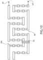
- This test can detect a short-circuit between the two serpentines (that of structure 38 and that of line 46), as exemplified in Figure 10 by undesired connection 50. All other elements of Figure 10 correspond to those of Figure 7A , already discussed. In case a short-circuit is present, high current (above a certain threshold, pre-set) is detected by the probe and the defect is revealed.
- Figure 11 shows a further embodiment of the present invention.
- the embodiment of figure 11 is based on the embodiment of Figure 8 (corresponding elements are identified with the same reference numerals and not further described).
- the conductive line 46 is designed and manufactured to be structurally and/or electrically equivalent or equal to the conductive segment 38a (as well as conductive segments 38b-38d).
- the conductive line 46 is, in the embodiment of Figure 11 , schematically depicted as a RC electrical structure. Even though Figure 11 is based on Figure 8 , the proposed design of conductive line 46 applies equally to the embodiment of Figures 9 .
- the provision of a multi sensor on a single chip, the sensor resistance conversion into a measurable frequency and the use of a dual serpentine interleaved sensor provide (singularly or in combination) the following advantages: reduced test time, improved screening, possibility of differential screening (among the four sensors) on chip, provision of a first level of topographical fault localization, fine measure of the sensor resistance, improvement of the correlation capability required for acceptance limit capability tuning.
Landscapes
- Chemical & Material Sciences (AREA)
- General Physics & Mathematics (AREA)
- Physics & Mathematics (AREA)
- Life Sciences & Earth Sciences (AREA)
- Biochemistry (AREA)
- Chemical Kinetics & Catalysis (AREA)
- Electrochemistry (AREA)
- Health & Medical Sciences (AREA)
- Pathology (AREA)
- Analytical Chemistry (AREA)
- Immunology (AREA)
- General Health & Medical Sciences (AREA)
- General Engineering & Computer Science (AREA)
- Engineering & Computer Science (AREA)
- Testing Of Individual Semiconductor Devices (AREA)
- Testing Or Measuring Of Semiconductors Or The Like (AREA)
- Investigating Or Analyzing Materials By The Use Of Electric Means (AREA)
Abstract
Description
- The present invention relates to an assembly for detecting a structural defect in a semiconductor die.
- Wafer singulation process for dice is a sensitive manufacturing step (specifically for LowK and ultra-LowK technologies). To secure this process, it is possible to detect failures linked to chipping and cracks in the seal ring of the dice (during the "Back-end-Of-Line", BEOL, manufacturing phase), using a so-called crack detector.
- With reference to
Figure 1 , adie 10 is shown in a top-plan view, and includes a crack sensor, or detector, 1. Thecrack sensor 1 is, in one exemplary embodiment of the known art, formed by several elements: - a conductive line 2 (having an own resistance), arranged either in a
seal ring area 4 of thedie 10 or in between theseal ring 4 and a sawingstreet 6; - a
detector cell 8, arranged in a I/O ring 7 of the die 10; and - a
test logic 9, embedded in acore portion 5 of the die 10, configured to test theresistive sensor 1 using thedetector cell 8. - The
conductive line 2 is substantially a continuous strip of conductive material, having a certain resistance, extending between two electrical nodes E1, E2. Theconductive line 2 can be formed by one or two sub-lines; in case of two sub-lines, one sub-line is placed between theseal ring area 4 and the I/O ring 7, and is also known as "inner sensor", and the other sub-line is placed within theseal ring area 4 and is also known as "outer sensor". Each sub-line is realized as a via chain (seeFigure 2 ). This solution with two sub-lines, or sub-sensors, permits to detect, in addition to cracks, also delamination defects. Considering the outer sensor, N-well straps may be inserted in the sensors terminals in order not to "break" the metal continuity of theseal ring area 4. - Measuring the electrical continuity of the
sensor 1 during EWS (Electrical Wafer Sorting") and FT ("Final Test") through thedetector cell 8 allows to detect, and screen out, portions of the seal ring having cracks. Affecting a specific bin and SBL to this test will allow a correct monitoring of the defect rate and to take adequate actions in case of need. - The use of the
sensor 1 improves the robustness of the chip product, enables detection of cracks in the BEOL at "time zero", which prevents delivery of weak parts that become failed parts in the customer application (when thermomechanical or humidity constraints play a major role). Use ofsensor 1 has a negligible impact on test time (it requires to test of a simple resistor), and does not introduce disturbances of functionality for RF products. -
Figure 2 , as anticipated, shows a cross-sectional view of an embodiment of (a portion of) acrack sensor 1 according to the known art. Thecrack sensor 1 ofFigure 2 may be used for chips with an interconnect structure of more than two metal layers. Substrateconductive segments 11 are arranged in asubstrate 12. A first portion of the substrateconductive segment 11 is connected to a firstconductive segment 14 in the M1 metallization level. A second portion of the substrateconductive segment 11 is connected to a secondconductive segment 15 in the M1 metallization level. The firstconductive segment 14 is connected to a plurality of furtherconductive segments 16 in upper metallization levels through a plurality of interlayer connects. Analogously, the secondconductive segment 15 is connected to a plurality of furtherconductive segments 18 in upper metallization levels through a plurality of respective interlayer connects. - The interlayer connects may comprise contacts and/or plugs/vias.
- The structure of
Figures 1 and2 may be used to detect cracks that may form when thedies 10 are separated (singulated) from the wafer. As said, the crack detector is a resistive sensor composed of a metal wire with two electrical nodes. This metal wire is placed around the die close to seal ring. Measuring the continuity of this wire allows to detect cracks. - To test the die 10 for cracks a voltage is applied across the electrical nodes E1, E2. A current flows during the application of the voltage to the two nodes E1, E2. If there is no (or almost no) voltage drop over the
resistive line 2, the sensor is intact and a crack is not disrupted or broken. If there is some voltage drop over theresistive line 2, the sensor may partially be broken, and if there is a complete or almost complete voltage drop over theresistive line 2, the sensor may be cut or severely damaged. - Some limitations apply to this solution. In particular, a large dispersion of sensor resistance, due to process variations, may be present, and therefore it is difficult to set reliable limits; moreover, the test requires long time to be completed (around 10ms); furthermore, the measurement requires off-chip arrangement.
- As an alternative solution, a digital testing can also be carried out.
-
Figure 3 shows a circuit design for performing digital testing. - In this example, a digital signal DATAIN is set as input to electrical node E1 of the
crack sensor 1. Signal DATAIN goes from digital value "0" to digital value "1". Aninput buffer stage 20 is provided to receive the signal DATAIN, rectify the signal DATAIN and drive properly thecrack sensor 1 through node E1. Anoutput buffer stage 21 is provided coupled to output electrical node E2 of thecrack sensor 1, to receive the signal that propagates through thecrack sensor 1, rectify the signal and provide at output a digital signal SOUT. - In one possible implementation, the signal DATAIN is generated by the
test logic 9, and theinput buffer stage 20 is part of thedetector cell 8, analogously, the signal SOUT is received by thetest logic 9 and theoutput buffer stage 21 is part of thedetector cell 8. - In case no cracks are present (i.e., the
resistive line 2 is not interrupted by a crack), the signal SOUT corresponds to the signal DATAIN, and is received with a certain time delay. On the contrary, in case of interruptions of theresistive line 2, no signal SOUT is received, or the signal SOUT considerably differs from the signal DATAIN. A crack, or another issue along theresistive line 2, is thus revealed. - Some limitations emerge from the use of the solution of
Figure 3 . - In particular, the users experience a large dispersion of sensor's RC constant (due to manufacturing process variations), therefore it would be difficult to set reliable limits; moreover, it is difficult to measure the exact transition time (since a sampling window should be fixed). Furthermore, this measurement requires off-chip arrangement.
- Patent document
DE102004028695 relates to a semiconductor component having a semiconductor body which has an edge, a central region and an edge region arranged between the edge and the central region. - Patent document
US 2015/115266 relates generally to semiconductor device fabrication and more specifically to detecting cracks in semiconductor substrates. - Patent document
US 2014/049284 relates to a test device for testing a semiconductor device, a semiconductor device, a semiconductor device and a testing method thereof and more particularly to a test device for testing a semiconductor device, a semiconductor device and a testing method thereof to test whether a TSV (Thru Silicon Via) included in a semiconductor device is formed without defects such as a crack therein and whether the TSV is connected to a metal layer or not. - However, the above-mentioned issues are not solved.
- The aim of the present invention is to overcome the problems previously illustrated.
- According to the present invention an assembly for detecting a structural defect in a semiconductor die is provided, as defined in
claim 1. - For a better understanding of the present invention, preferred embodiments thereof are now described, purely by way of non-limiting example and with reference to the attached drawings, wherein:
-
Figure 1 is a top view of a semiconductor die including a crack detector according to the known art; -
Figure 2 is a section view of a crack detector according to the known art, from which it can be appreciated that the crack detector is formed in a plurality of metal layers and vias; -
Figure 3 shows a circuit to perform digital measures of the crack detector, according to the known art; -
Figure 4 is a top view of a semiconductor die including a crack detector according to an embodiment the present invention; -
Figure 5 schematically shows an electrical representation of a portion of a crack detector provided with a mono-directional oscillating ring, according to an embodiment of the present invention; -
Figure 6 schematically shows an electrical representation of a portion of a crack detector provided with a bi-directional oscillating ring, according to a further embodiment of the present invention; -
Figure 7A is a schematic section view of a portion of the crack detector, according to an embodiment of the present invention; -
Figure 7B is a top view of the semiconductor die including the crack detector according to the embodiment offigure 7A ; -
Figure 8 shows an electrical representation of a portion of a crack detector to perform a resistive measurement, according to an embodiment of the present invention; -
Figure 9 shows an electrical representation of a portion of a crack detector to perform a leakage test, according to an embodiment of the present invention; -
Figure 10 is a section view corresponding to the view ofFigure 7A , where a defect causing current leakage is present, which can be detected by the crack sensor ofFigure 9 ; and -
Figure 11 shows an electrical representation of a portion of a crack detector to perform a resistive measurement, according to a further embodiment of the present invention. -
Figure 4 shows a die 30 housing a crack-detection sensor 32 (in the following also referred to as "crack sensor"), according to an embodiment of the present invention. - In a way not shown in the drawings, the
die 30 derives from a semiconductor wafer comprising a plurality of dies 30 formed across a top surface of the wafer, after the semiconductor dies have been diced (i.e., cut into individual dies from a wafer). Thedie 30 is typically square or rectangular in shape. Thedie 30 comprises an integrated circuit (not shown in detail). - After manufacturing of a plurality of dies on the wafer, the plurality of dies are separated from one another along scribe lines (the so-called "singulation" step). The scribe lines are located at the perimeter of the die 30, so that at the end of the manufacturing process a saw can be used to detach one die from adjacent dies along the scribe lines. The singulation of the dies may also be performed, for example, by laser dicing or laser scribing followed by saw dicing.
- The
crack sensor 32 is formed in at least one conductive-material layer (metal layer) of the die 30, more preferably in a plurality of overlying metal layers separated from one another by dielectric or insulating layers and connected by means of vias passing through such dielectric or insulating layers. Thecrack sensor 32 is, in particular, formed at least in part along aperimeter region 34 of the die 30, as shown inFigure 4 . In detail, thecrack sensor 32 is formed between anedge 32a of thedie 32 and aninterior region 32b of the die 32, wherein theinterior region 32b houses the integrated circuit. In one embodiment, a seal region, or seal ring, 36 is also present between theedge 32a and theinterior region 32b. A seal ring is, for example, a multi-layer structure composed of alternating conducting and insulating layers. Through each of the insulating layers run multiple vias which provide electrical paths between adjacent metal layers. The lowest layer of metal in the seal structure makes electrical contact with the substrate, which can be either p-type or n-type. Theseal ring 36 may be omitted. - The
crack sensor 32 comprises aresistive structure 38 of conductive material having a certain electrical resistance, which extends, or is integrated, proximate theedge 32a, at least in part between (in a top view) theseal ring 36 and theedge 32a. Theresistive structure 38 comprises a plurality ofresistive segments 38a-38d of conductive material having a certain electrical resistance (in the following, also named "conductive segments"), formed in one or more metal layers of the die 30; in other words, the conductive structure is formed in a plurality of metal layers in a multi-level interconnect system, wherein vias are used to connect one metal level to another (analogously to the prior art shown inFigure 2 ). Eachconductive segment 38a-d comprises a first end 39' and asecond end 39". - While the
conductive segments 38a-d extends mainly along theedge 32a, the first end 39' and thesecond end 39" are in theinterior region 32b (therefore, at least a portion of theconductive segments 38a-d extends from theedge 32a to theinterior region 32b, or viceversa, through the seal ring 36). The first end 39' and thesecond end 39" of eachconductive segment 38a-d are coupled to respective end portions of arespective oscillator module 40a-40d; eachoscillator module 40a-40d includes elements (in particular, in one embodiment, passive electronic devices) configured for generating an oscillating signals, having an own frequency, throughout theconductive segment 38a-38d. The frequency of the oscillating signals can be used for checking the structural integrity of thedie 30. In fact, the frequencies of the oscillating signals in eachconductive segment 38a-38d, can be measured and compared with a reference frequency (pre-set value), or compared with one another. In case of comparison with a reference frequency, the result of the comparison is indicative of the presence of a defect. In case of comparison of one frequency with another frequency (belonging todifferent segments 38a-38d), the result of the comparison is indicative of the presence of a defect. - Computing means, such as a
microcontroller 43, are present to perform operations aimed at verifying the presence of the structural defect, as better discussed later. Themicrocontroller 43 can be integrated in the semiconductor die 30 (in theregion 32b), or arranged external to the semiconductor die 30. Themicrocontroller 43 is operatively coupled to theoscillator modules 40a-40d. - In detail, if the frequency in one
conductive segment 38a-38d is different from the reference frequency (expected frequency), a structural defect is probably present at the region of the die 30 housing such conductive segment. The detection can be carried out by comparing, by themicrocontroller 43, the frequency of the oscillating signal in theconductive segment 38a-38d under test with an expected frequency value (predefined, stored in a memory). Tolerances can be set when performing such frequency comparison. - When the frequency of a signal in one
conductive segment 38a-38d is compared with the frequencies of the signals in the otherconductive segments 38a-38d, a structural defect is detected when the frequencies are not equal or substantially equal to one another. In this case, a differential measurement is performed. For example, the two frequencies belonging to two respectiveconductive segments 38a-38d are subtracted, and the result (the difference) is checked with respect to a predefined range of expected values. In particular, if the difference is greater that a threshold, the two frequencies are deemed to be different from one another and a defect in thedie 30 is detected. - Also in this case, tolerances can be set when performing such frequency comparison. The detection can be carried out by comparing, by the
microcontroller 43, the frequency of the oscillating signal in theconductive segment 38a-38d under test with the frequency of the oscillating signal in one or more of the otherconductive segments 38a-38d. In this latter case, the defect is detected if the measured frequency for the conductive segment under test is substantially different from the frequency measured in the otherconductive segments 38b-38d. In principle, it is not important to know which frequency is "correct", i.e. that of the segment under test or that of the other segment(s). In fact, as long as a defect is detected, theentire die 30 is to be put aside / replaced. - Absence of the oscillating signal is also an indication of the presence of a structural defect.
- With specific reference to the embodiment of
Figure 4 , fouroscillator modules 40a-40d are arranged withinregion 32b. With the present solution, using fourconductive segments 38a-d instead of a single conductive segment (as in the known art), and performing separate frequency measurements for each of them, provide a precise indication of the possible defectivity (associated to a crack or delamination of the respective portion of the die 30) of thedie 30 under test. - The approach that foresees reciprocal comparison of the frequencies of the signals in the
segments 38a-38d requires that allconductive segments 38a-38d andoscillator modules microcontroller 43 performing the comparisons. The detection of the issue (crack, leakage, etc.) is, in this approach, not dependent on absolute parameters, but depends on a relative error detected in oneconductive segment 38a-38d with respect to the measurements done in the other conductive segments38a-38d. - In an alternative embodiment, the absolute range of the measured parameter across PVT can anyway also be checked.
- With reference to
Figure 5 , theconductive segment 38a and theoscillator module 40a coupled to theconductive segment 38a are shown in details, according to one embodiment. - In the embodiment of
Figure 5 , the detection is performed by looping eachconductive segment 38a-38d (here, as said, onlysegment 38a is shown as an example) as an oscillating structure employing passive elements only. Theoscillator module 40a (oscillator modules 40b-40d are analogous) includes achain 45 formed by the series of an odd number of NOT gates orinverters inverter 45a is connected to the first end 39' ofsegment 38a; the output port ofinverter 45a is connected to input port ofinverter 45b; output port ofinverter 45b is connected to input port ofinverter 45c; and output port ofinverter 45c is connected tosecond end 39" ofsegment 38a. the connection of the output port ofinverter 45c to thesecond end 39" is formed by aconductive line 46 that runs through theregion 32b of the die 30 (as depicted schematically infigure 4 with dashed line) or, alternatively, along the periphery of the die 30, analogously tosegment 38a (seeFigure 7B ). - The
resistive structure 38 is schematically depicted as a RC electrical structure. - By connecting the
chain 45 to both ends 39', 39" of theconductive segment 38a, thus forming a closed loop, a ring oscillator is formed. A frequency signal is therefore generated and can be detected by themicrocontroller 43. The ring oscillator in this example comprises three tri-state inverters in a ring, whose output oscillates between two voltage levels, representing "true" and "false" logic states. The enabling signal SE1 is used to activate and deactivate theoscillator module 40a, when requested during use. For example, when SE="1", the inverters are "on" (or "active" or in "conduction state"), and theoscillator module 40a starts oscillating and a frequency can be observed at any point in the loop; such frequency can be measured through known means and techniques. - For example, the
microcontroller 43 is coupled to theinverters 45a-c in thechain 45 to provide the activation signal SE1 only when a test is to be performed, and deactivate the inventers otherwise. - There can be multiple methods to measure the frequency in the loop. In one exemplary embodiment, the analysis of the frequency can be done by acquiring, by the
microcontroller 43, the signal in the ring oscillator (e.g., the signal present at the output port of anyone of the inverters in the chain 45) and counting the rising edges of such signal. To measure the frequency, other parameters of the signal can be checked by the microcontroller 43 (for examples the falling edge of the signal, or the logic states "0" or "1" of the signal). The frequency thus measured can, as already discussed, be compared with a pre-set value (e.g. stored in a memory) or compared with the measured frequencies of the signal in one or more of the otherconductive segments 38b-38d /chains 45. - The circuit shown is capable to finely measure, during testing, the frequency and therefore the effective RC. Fine measures provide the capability of correlation between:
- Native measure at EWS;
- Values measured at FT (being sawing major source of cracks);
- Hard failures after stress (Burn-In, soldering, thermal cycles) characterization;
- Hard failures from the field.
- The RC constant of the conductive segment is dominant with respect to CMOS elements (i.e., the inverters of the chain 45), therefore allowing a frequency measure that is substantially immune from undesired contributions.
-
Figure 6 shows a further embodiment of one oscillator module (here, forexample oscillator module 40a, but theother oscillator modules 40b-40d are the same), where a bidirectional oscillating structure 45' is employed and implemented. Here, eachinverter 45a-45c in the chain is arranged in electrical parallel with anotherinverter 45d-45f, to allow the generation of an oscillating signal in both clockwise and counter clockwise directions. When a signal in clockwise direction is to be generated, the correspondinginverters 45a-45c are turned on by setting signal SE1="1", and theother inverters 45d-45f are turned off by setting signal SE2="0". When a signal in counter clockwise direction is to be generated, the correspondinginverters 45d-45f are turned on by setting signal SE2="1", and theother inverters 45a-45c are turned off by setting signal SE1="0" - In this embodiment, the effect of an abnormal resistance of a portion of the
conductive segment 38a (due to e.g. a crack or partial crack) can be detected by comparing together the frequencies of the two signals in clockwise and counter clockwise directions for the sameconductive segment 38a. In this case, a differential measurement is performed. For example, the two frequencies of signals in clockwise and counter clockwise directions are subtracted from one another, and the result (the difference) is checked with respect to a predefined range of expected values. In particular, if the difference is greater that a threshold, the two frequencies are deemed to be different from one another and a defect in thedie 30 is detected. - A structural defect that affect only a portion of the
conductive segment 38a increases locally the electrical resistance of theconductive segment 38a (the same applies to otherconductive segments 38b-38d). A high-resistance in one portion only of theconductive segment 38a may reduce the frequency of the clockwise signal (such frequency being lower than the expected value). On the contrary, the frequency of the counter clockwise signal may be differently affected, or not affected at all. Therefore, by comparing the two frequencies together provides an indication of the presence, or absence, of a defect in thesegment 38a under test. This method can be applied to the circuit topology according to the present invention, as well as to the circuit topologies of the known art. -
Figure 7A shows a structural implementation of theconductive segment 38a (theother segments 38b-d being equivalent) and of theconductive line 46 connecting thesecond end 39" to thechain 45, when suchconductive line 46 is formed at the periphery of the die 30, i.e. out ofregion 32b and, more in particular, between theseal ring 36 and theedge 32a. theconductive line 46 is formed through various metal layers, analogously to conductive segment 38a.In this case, in fact, theconductive segment 38a-38d and the respectiveconductive line 46 are formed as two interleaved metal and via serpentines, with the two ends 39' and 39" connected to thechain 45 or 45', as already shown inFigures 5 and6 . - In a further embodiment,
Figure 8 , a defect can be detected by a resistance measurement. This can be done by applying a voltage through a probe and check the current from it, to calculate the resistance in a per se known way. Allinverters 45a-45f of the bi-directional oscillating structure 45' are disabled (SE1=SE"="0") during this test. - A number of switches (represented as transistors) are coupled to the crack sensor in order to perform this test. In particular, a
switch 60 connects the first end 39' to the probe pad, to supply a test current to first end 39'; aswitch 62 connects thesecond end 39" to the ground; aswitch 63 connects thesecond end 39" to theconductive line 46; and aswitch 64 connects theconductive line 46 to the ground. - To perform a resistive test of
conductive segment 38a, switches 60 and 62 are turned on, and switches 63 and 64 are turned off. A test current flows from the probe pad to the ground, passing through theconductive line 38. An electrical resistance ofsegment 38a can be measured in a known way, and compared with an expected value. A result of such comparison is indicative of an abnormal resistance insegment 38a, which may indicate the presence of a structural defect. - Alternatively, the electrical resistance of
segment 38a can be measured and compared with the electrical resistance of another segment, forexample segment 38b. In this case, a differential measurement is performed. For example, the two resistance values belonging to two respectiveconductive segments die 30 is detected. - In a further embodiment,
Figure 9 , a leakage test can be carried out. To do so, a voltage is applied through a probe and the current from it is checked; ideally such current should be negligible. All inverters of the oscillating structure 45' are disabled, or not present, during this test, as inFigure 8 . During this test, switch 60 is on, to connect the first end 39' to the probe pad, for supplying the test current. It is noted thatswitch 64 is also turned on, to connectconductive line 46 to ground. Allother switches structure 38 and that of line 46), as exemplified inFigure 10 byundesired connection 50. All other elements ofFigure 10 correspond to those ofFigure 7A , already discussed. In case a short-circuit is present, high current (above a certain threshold, pre-set) is detected by the probe and the defect is revealed. -
Figure 11 shows a further embodiment of the present invention. The embodiment offigure 11 is based on the embodiment ofFigure 8 (corresponding elements are identified with the same reference numerals and not further described). Infigure 11 , theconductive line 46 is designed and manufactured to be structurally and/or electrically equivalent or equal to theconductive segment 38a (as well asconductive segments 38b-38d). Theconductive line 46 is, in the embodiment ofFigure 11 , schematically depicted as a RC electrical structure. Even thoughFigure 11 is based onFigure 8 , the proposed design ofconductive line 46 applies equally to the embodiment ofFigures 9 . - The advantages of the invention described previously, according to the various embodiments, emerge clearly from the foregoing description.
- In particular, the provision of a multi sensor on a single chip, the sensor resistance conversion into a measurable frequency and the use of a dual serpentine interleaved sensor, provide (singularly or in combination) the following advantages: reduced test time, improved screening, possibility of differential screening (among the four sensors) on chip, provision of a first level of topographical fault localization, fine measure of the sensor resistance, improvement of the correlation capability required for acceptance limit capability tuning.
- Finally, it is clear that modifications and variations may be made to what has been described and illustrated herein, without thereby departing from the scope of the present invention, as defined in the annexed claims.
Claims (14)
- An assembly for detecting a structural defect in a semiconductor die (30), comprising a defect-detection sensor and computing means (43),wherein the defect-detection sensor includes:a resistive structure (38) comprising a plurality of resistive paths (38a-d) of electrical-conductive material in the semiconductor die (30), each resistive path (38a-d) having a first end (39') and a second end (39") and extending in a respective region of the semiconductor die proximate a perimeter (32a) of the semiconductor die, partially encircling an interior portion (32b) of the semiconductor die (30); anda plurality of signal-generation structures (40a-40d, 45), each of which is electrically coupled to the first end (39') and the second end (39") of a respective resistive path (38a-d) and is configured to supply a respective test signal to the resistive path (38a-d);and wherein the computing means (43) are operatively coupled to the plurality of signal-generation structures (40a-40d, 45), and are configured to:control the signal-generation structures (40a-40d, 45) to generate the test signals;acquire the test signals in each resistive paths (38a-d) ;test an electrical feature of the resistive paths (38a-d) by performing an analysis of the test signals acquired; anddetect the presence of said structural defect in the semiconductor die (30) based on a result of said analysis of the test signals acquired.
- The assembly of claim 1, wherein each resistive path (38a-d) includes a loop formed by a first sub-path extending from the first end (39') to an intermediate connection point and a second sub-path extending from the intermediate connection point to the second end (39").
- The assembly of claim 1 or claim 2, wherein the semiconductor die (30) comprises a seal ring (36) encircling the interior portion (32b), each resistive path (38a-d) extending between the seal ring (36) and the perimeter (32a) with the exception of the first and the second ends (39'0, 39") that extend through the seal ring (36) towards the interior portion (32b).
- The assembly of anyone of the preceding claims, wherein each signal-generation structure (40a-40d, 45) comprises a current generator that can be activated to supply the test signal, which is an electrical current, to the respective resistive path (38a-d);
and wherein the computing means (43) are configured to:control the signal-generation structures (40a-40d, 45) by activating the current generator;test the electrical feature of the resistive paths (38a-d) by measuring an electrical resistance value that each resistive path (38a-d) opposes to the flow of the electrical current. - The assembly of claim 4, wherein the computing means (43) are further configured to test the electrical feature of the resistive paths (38a-d) by performing a differential measurement of the electrical resistance values among said plurality of resistive paths (38a-d).
- The assembly of claim 5, wherein said defect is detected if a result of the differential measurement is out of a predefined range of expected values.
- The assembly of anyone of claims 1-3, wherein each signal-generation structure (40a-40d, 45) comprises an oscillator device (45') including an odd number of inverters (45a-45c) connected in electrical series to one another between the first end (39') and the second end (39"), said oscillator device (45') forming, with the respective resistive path (38a-d) to which it is coupled, a mono-directional ring oscillator.
- The assembly of anyone of claims 1-3, wherein each signal-generation structure (40a-40d, 45) comprises an oscillator device (45') including a first set of inverters (45a-45c) in odd number connected in electrical series to one another between the first end (39') and the second end (39"), and a second set of inverters (45d-45f) in odd number connected in electrical series to one another between the first end (39') and the second end (39") in antiparallel connection with respect to the first set of inverters (45a-45c),
said oscillator device (45') forming, with the respective resistive path (38a-d) to which it is coupled, a bi-directional ring oscillator. - The assembly of anyone of claims 7-8, wherein the test signal is an oscillation signal having an oscillation frequency, the computing means (43) being configured to test the electrical feature of the resistive paths (38a-d) by performing an analysis of the oscillation frequency of the test signal belonging to the resistive path (38a-d) under test.
- The assembly of claim 9, wherein the computing means (43) are configured to perform said analysis of the oscillation frequency by comparing the oscillation frequency of the test signal belonging to the resistive path (38a-d) under test with a frequency of another test signal belonging to another resistive path (38a-d) of the plurality of resistive paths (38a-38d).
- The assembly of claim 9 or 10, wherein the computing means (43) are configured to perform said analysis of the oscillation frequency by performing a differential measurement the oscillation frequency of the test signal belonging to the resistive path (38a-d) under test with a frequency of another test signal belonging to another resistive path (38a-d) of the plurality of resistive paths (38a-38d) .
- The assembly of claim 11, wherein said defect is detected if a result of the differential measurement is out of a predefined range of expected values.
- The assembly of claim 9, wherein the computing means (43) are configured to perform said analysis of the oscillation frequency by comparing the oscillation frequency of the test signal belonging to the resistive path (38a-d) under test with an expected reference frequency.
- The assembly of claim 8, or claim 9 when depending upon claim 8, wherein the computing means (43) are further configured to test one resistive path (38a-38d) by:activate the first set of inverters (45a-45c) coupled to said resistive path (38a-38d) under test, thus causing the generation of one respective test signal flowing in a first direction through the resistive path (38a-38d) under test and, at the same time, deactivate the second set of inverters (45d-45f) coupled in antiparallel connection to the activated first set of inverters (45a-45c) of said resistive path (38a-38d) under test;acquire a first frequency value of the test signal flowing in said first direction;deactivate the first set of inverters (45a-45c) coupled to the resistive path (38a-38d) under test, and, at the same time, activate the second set of inverters (45d-45f) coupled to the resistive path (38a-38d) under test, thus causing the generation of another test signal flowing in a second direction, opposed to the first direction, through the resistive path (38a-38d) under test;acquire a second frequency value of the test signal flowing in said second direction;compare the first frequency value with the second frequency value;associate a physical state of the semiconductor die (30) to a result of said comparison of the first frequency value with the second frequency value.
Applications Claiming Priority (1)
| Application Number | Priority Date | Filing Date | Title |
|---|---|---|---|
| IT102021000030482A IT202100030482A1 (en) | 2021-12-01 | 2021-12-01 | CRACK DETECTOR FOR SEMICONDUCTOR DIAGRAM |
Publications (1)
| Publication Number | Publication Date |
|---|---|
| EP4191647A1 true EP4191647A1 (en) | 2023-06-07 |
Family
ID=80928773
Family Applications (1)
| Application Number | Title | Priority Date | Filing Date |
|---|---|---|---|
| EP22207185.4A Pending EP4191647A1 (en) | 2021-12-01 | 2022-11-14 | Crack detector for semiconductor dies |
Country Status (4)
| Country | Link |
|---|---|
| US (1) | US12613274B2 (en) |
| EP (1) | EP4191647A1 (en) |
| CN (1) | CN116203083A (en) |
| IT (1) | IT202100030482A1 (en) |
Families Citing this family (2)
| Publication number | Priority date | Publication date | Assignee | Title |
|---|---|---|---|---|
| CN219179280U (en) * | 2022-11-18 | 2023-06-13 | 三赢科技(深圳)有限公司 | Substrates with Crack Detection |
| TW202537104A (en) * | 2024-02-06 | 2025-09-16 | 聯發科技股份有限公司 | Semiconductor device |
Citations (7)
| Publication number | Priority date | Publication date | Assignee | Title |
|---|---|---|---|---|
| DE102004028695B3 (en) | 2004-06-14 | 2005-12-22 | Infineon Technologies Ag | Breakage sensor for installation near edge of semiconductor substrate has isolation layer and several electrode layers with terminals connected to sensor circuit |
| US20090321734A1 (en) * | 2008-06-30 | 2009-12-31 | Texas Instruments Incorporated | Capacitor-based method for determining and characterizing scribe seal integrity and integrity loss |
| US20100184287A1 (en) * | 2009-01-22 | 2010-07-22 | Hynix Semiconductor Inc. | Method of Forming Patterns of Semiconductor Device |
| US20140049284A1 (en) | 2012-08-14 | 2014-02-20 | Korea Advanced Institute Of Science And Technology | Test device, semiconductor device and testing method thereof |
| US20140375341A1 (en) * | 2013-06-20 | 2014-12-25 | Freescale Semiconductor, Inc. | Die Fracture Detection and Humidity Protection with Double Guard Ring Arrangement |
| US20150115266A1 (en) | 2013-10-28 | 2015-04-30 | Freescale Semiconductor, Inc. | Die crack detector with integrated one-time programmable element |
| US20210366794A1 (en) * | 2018-08-29 | 2021-11-25 | Taiwan Semiconductor Manufacturing Company Ltd. | Method for detecting defects in semiconductor device |
Family Cites Families (7)
| Publication number | Priority date | Publication date | Assignee | Title |
|---|---|---|---|---|
| TW486806B (en) * | 1998-10-30 | 2002-05-11 | Hitachi Ltd | Semiconductor integrated circuit apparatus and IC card |
| KR100318431B1 (en) * | 1999-12-24 | 2001-12-24 | 박종섭 | A very compact Delay Locked Loop using bi-directional ring oscillator and counter |
| US7489204B2 (en) * | 2005-06-30 | 2009-02-10 | International Business Machines Corporation | Method and structure for chip-level testing of wire delay independent of silicon delay |
| JP5034781B2 (en) * | 2007-08-27 | 2012-09-26 | 富士通株式会社 | High-sensitivity resistance measuring device and monitoring method for solder bump |
| JP2012074674A (en) * | 2010-09-02 | 2012-04-12 | Canon Inc | Semiconductor integrated circuit device |
| US11215661B2 (en) * | 2020-05-12 | 2022-01-04 | Globalfoundries U.S. Inc. | Cascaded sensing circuits for detecting and monitoring cracks in an integrated circuit |
| KR20220128718A (en) * | 2021-03-15 | 2022-09-22 | 에스케이하이닉스 주식회사 | Semiconductor device with crack detection ring and crack detection structure |
-
2021
- 2021-12-01 IT IT102021000030482A patent/IT202100030482A1/en unknown
-
2022
- 2022-11-08 US US18/053,688 patent/US12613274B2/en active Active
- 2022-11-14 EP EP22207185.4A patent/EP4191647A1/en active Pending
- 2022-11-30 CN CN202211543632.3A patent/CN116203083A/en active Pending
Patent Citations (7)
| Publication number | Priority date | Publication date | Assignee | Title |
|---|---|---|---|---|
| DE102004028695B3 (en) | 2004-06-14 | 2005-12-22 | Infineon Technologies Ag | Breakage sensor for installation near edge of semiconductor substrate has isolation layer and several electrode layers with terminals connected to sensor circuit |
| US20090321734A1 (en) * | 2008-06-30 | 2009-12-31 | Texas Instruments Incorporated | Capacitor-based method for determining and characterizing scribe seal integrity and integrity loss |
| US20100184287A1 (en) * | 2009-01-22 | 2010-07-22 | Hynix Semiconductor Inc. | Method of Forming Patterns of Semiconductor Device |
| US20140049284A1 (en) | 2012-08-14 | 2014-02-20 | Korea Advanced Institute Of Science And Technology | Test device, semiconductor device and testing method thereof |
| US20140375341A1 (en) * | 2013-06-20 | 2014-12-25 | Freescale Semiconductor, Inc. | Die Fracture Detection and Humidity Protection with Double Guard Ring Arrangement |
| US20150115266A1 (en) | 2013-10-28 | 2015-04-30 | Freescale Semiconductor, Inc. | Die crack detector with integrated one-time programmable element |
| US20210366794A1 (en) * | 2018-08-29 | 2021-11-25 | Taiwan Semiconductor Manufacturing Company Ltd. | Method for detecting defects in semiconductor device |
Also Published As
| Publication number | Publication date |
|---|---|
| US12613274B2 (en) | 2026-04-28 |
| CN116203083A (en) | 2023-06-02 |
| IT202100030482A1 (en) | 2023-06-01 |
| US20230168300A1 (en) | 2023-06-01 |
Similar Documents
| Publication | Publication Date | Title |
|---|---|---|
| US12613274B2 (en) | Crack detector for semiconductor dies | |
| JP6444914B2 (en) | Semiconductor device | |
| US7557597B2 (en) | Stacked chip security | |
| US7471101B2 (en) | Systems and methods for controlling of electro-migration | |
| US7649200B1 (en) | System and method of detecting IC die cracks | |
| US7489204B2 (en) | Method and structure for chip-level testing of wire delay independent of silicon delay | |
| JP2008021864A (en) | Semiconductor device | |
| US9146273B2 (en) | Process for controlling the correct positioning of test probes on terminations of electronic devices integrated on a semiconductor and corresponding electronic device | |
| US20100315114A1 (en) | Semiconductor device with test structure and semiconductor device test method | |
| US20110187396A1 (en) | Quiescent current (iddq) indication and testing apparatus and methods | |
| KR101846562B1 (en) | Semiconductor test device, semiconductor device and method for testing semiconductor device | |
| US7622940B2 (en) | Semiconductor device having contact failure detector | |
| US8253420B2 (en) | Integrated electrical circuit and test to determine the integrity of a silicon die | |
| JP2007158346A (en) | Probe sensing pad and probe needle contact position inspection method | |
| US8362795B2 (en) | Semiconductor device capable of verifying reliability | |
| US20090121733A1 (en) | Test circuit for use in a semiconductor apparatus | |
| US10935590B2 (en) | Electrically-verifiable fuses and method of fuse verification | |
| KR20140128620A (en) | Apparatus of Detecting Mis-alignment of Test Pad | |
| CN121878434A (en) | A self-detection circuit, method, and ASIC chip for chip peeling cracks | |
| JP2014033000A (en) | Semiconductor device and testing method of semiconductor device | |
| TWI871896B (en) | Circuit for detecting via degradation, method of testing a plurality of vias and testing system | |
| CN118299368B (en) | A 2.5D packaged test integrated circuit, test method and packaging method | |
| KR101575959B1 (en) | Probe tester and probe test method | |
| JP2014163851A (en) | Semiconductor integrated circuit with open detection terminal | |
| JP2004045258A (en) | Probe card |
Legal Events
| Date | Code | Title | Description |
|---|---|---|---|
| PUAI | Public reference made under article 153(3) epc to a published international application that has entered the european phase |
Free format text: ORIGINAL CODE: 0009012 |
|
| STAA | Information on the status of an ep patent application or granted ep patent |
Free format text: STATUS: THE APPLICATION HAS BEEN PUBLISHED |
|
| AK | Designated contracting states |
Kind code of ref document: A1 Designated state(s): AL AT BE BG CH CY CZ DE DK EE ES FI FR GB GR HR HU IE IS IT LI LT LU LV MC ME MK MT NL NO PL PT RO RS SE SI SK SM TR |
|
| STAA | Information on the status of an ep patent application or granted ep patent |
Free format text: STATUS: REQUEST FOR EXAMINATION WAS MADE |
|
| 17P | Request for examination filed |
Effective date: 20231128 |
|
| RBV | Designated contracting states (corrected) |
Designated state(s): AL AT BE BG CH CY CZ DE DK EE ES FI FR GB GR HR HU IE IS IT LI LT LU LV MC ME MK MT NL NO PL PT RO RS SE SI SK SM TR |
|
| STAA | Information on the status of an ep patent application or granted ep patent |
Free format text: STATUS: EXAMINATION IS IN PROGRESS |
|
| 17Q | First examination report despatched |
Effective date: 20250226 |