EP4191639A1 - Nitride semiconductor wafer and method for producing nitride semiconductor wafer - Google Patents
Nitride semiconductor wafer and method for producing nitride semiconductor wafer Download PDFInfo
- Publication number
- EP4191639A1 EP4191639A1 EP21850368.8A EP21850368A EP4191639A1 EP 4191639 A1 EP4191639 A1 EP 4191639A1 EP 21850368 A EP21850368 A EP 21850368A EP 4191639 A1 EP4191639 A1 EP 4191639A1
- Authority
- EP
- European Patent Office
- Prior art keywords
- nitride semiconductor
- silicon single
- crystal substrate
- semiconductor wafer
- atoms
- Prior art date
- Legal status (The legal status is an assumption and is not a legal conclusion. Google has not performed a legal analysis and makes no representation as to the accuracy of the status listed.)
- Pending
Links
Images

Classifications
-
- H—ELECTRICITY
- H10—SEMICONDUCTOR DEVICES; ELECTRIC SOLID-STATE DEVICES NOT OTHERWISE PROVIDED FOR
- H10D—INORGANIC ELECTRIC SEMICONDUCTOR DEVICES
- H10D62/00—Semiconductor bodies, or regions thereof, of devices having potential barriers
- H10D62/80—Semiconductor bodies, or regions thereof, of devices having potential barriers characterised by the materials
- H10D62/85—Semiconductor bodies, or regions thereof, of devices having potential barriers characterised by the materials being Group III-V materials, e.g. GaAs
- H10D62/8503—Nitride Group III-V materials, e.g. AlN or GaN
-
- H—ELECTRICITY
- H10—SEMICONDUCTOR DEVICES; ELECTRIC SOLID-STATE DEVICES NOT OTHERWISE PROVIDED FOR
- H10P—GENERIC PROCESSES OR APPARATUS FOR THE MANUFACTURE OR TREATMENT OF DEVICES COVERED BY CLASS H10
- H10P90/00—Preparation of wafers not covered by a single main group of this subclass, e.g. wafer reinforcement
-
- C—CHEMISTRY; METALLURGY
- C30—CRYSTAL GROWTH
- C30B—SINGLE-CRYSTAL GROWTH; UNIDIRECTIONAL SOLIDIFICATION OF EUTECTIC MATERIAL OR UNIDIRECTIONAL DEMIXING OF EUTECTOID MATERIAL; REFINING BY ZONE-MELTING OF MATERIAL; PRODUCTION OF A HOMOGENEOUS POLYCRYSTALLINE MATERIAL WITH DEFINED STRUCTURE; SINGLE CRYSTALS OR HOMOGENEOUS POLYCRYSTALLINE MATERIAL WITH DEFINED STRUCTURE; AFTER-TREATMENT OF SINGLE CRYSTALS OR A HOMOGENEOUS POLYCRYSTALLINE MATERIAL WITH DEFINED STRUCTURE; APPARATUS THEREFOR
- C30B25/00—Single-crystal growth by chemical reaction of reactive gases, e.g. chemical vapour-deposition growth
- C30B25/02—Epitaxial-layer growth
- C30B25/18—Epitaxial-layer growth characterised by the substrate
-
- C—CHEMISTRY; METALLURGY
- C30—CRYSTAL GROWTH
- C30B—SINGLE-CRYSTAL GROWTH; UNIDIRECTIONAL SOLIDIFICATION OF EUTECTIC MATERIAL OR UNIDIRECTIONAL DEMIXING OF EUTECTOID MATERIAL; REFINING BY ZONE-MELTING OF MATERIAL; PRODUCTION OF A HOMOGENEOUS POLYCRYSTALLINE MATERIAL WITH DEFINED STRUCTURE; SINGLE CRYSTALS OR HOMOGENEOUS POLYCRYSTALLINE MATERIAL WITH DEFINED STRUCTURE; AFTER-TREATMENT OF SINGLE CRYSTALS OR A HOMOGENEOUS POLYCRYSTALLINE MATERIAL WITH DEFINED STRUCTURE; APPARATUS THEREFOR
- C30B29/00—Single crystals or homogeneous polycrystalline material with defined structure characterised by the material or by their shape
- C30B29/02—Elements
- C30B29/06—Silicon
-
- C—CHEMISTRY; METALLURGY
- C30—CRYSTAL GROWTH
- C30B—SINGLE-CRYSTAL GROWTH; UNIDIRECTIONAL SOLIDIFICATION OF EUTECTIC MATERIAL OR UNIDIRECTIONAL DEMIXING OF EUTECTOID MATERIAL; REFINING BY ZONE-MELTING OF MATERIAL; PRODUCTION OF A HOMOGENEOUS POLYCRYSTALLINE MATERIAL WITH DEFINED STRUCTURE; SINGLE CRYSTALS OR HOMOGENEOUS POLYCRYSTALLINE MATERIAL WITH DEFINED STRUCTURE; AFTER-TREATMENT OF SINGLE CRYSTALS OR A HOMOGENEOUS POLYCRYSTALLINE MATERIAL WITH DEFINED STRUCTURE; APPARATUS THEREFOR
- C30B29/00—Single crystals or homogeneous polycrystalline material with defined structure characterised by the material or by their shape
- C30B29/10—Inorganic compounds or compositions
- C30B29/40—AIIIBV compounds wherein A is B, Al, Ga, In or Tl and B is N, P, As, Sb or Bi
- C30B29/403—AIII-nitrides
-
- H—ELECTRICITY
- H10—SEMICONDUCTOR DEVICES; ELECTRIC SOLID-STATE DEVICES NOT OTHERWISE PROVIDED FOR
- H10D—INORGANIC ELECTRIC SEMICONDUCTOR DEVICES
- H10D62/00—Semiconductor bodies, or regions thereof, of devices having potential barriers
- H10D62/40—Crystalline structures
-
- H—ELECTRICITY
- H10—SEMICONDUCTOR DEVICES; ELECTRIC SOLID-STATE DEVICES NOT OTHERWISE PROVIDED FOR
- H10P—GENERIC PROCESSES OR APPARATUS FOR THE MANUFACTURE OR TREATMENT OF DEVICES COVERED BY CLASS H10
- H10P14/00—Formation of materials, e.g. in the shape of layers or pillars
- H10P14/20—Formation of materials, e.g. in the shape of layers or pillars of semiconductor materials
- H10P14/29—Formation of materials, e.g. in the shape of layers or pillars of semiconductor materials characterised by the substrates
- H10P14/2901—Materials
- H10P14/2902—Materials being Group IVA materials
- H10P14/2905—Silicon, silicon germanium or germanium
-
- H—ELECTRICITY
- H10—SEMICONDUCTOR DEVICES; ELECTRIC SOLID-STATE DEVICES NOT OTHERWISE PROVIDED FOR
- H10P—GENERIC PROCESSES OR APPARATUS FOR THE MANUFACTURE OR TREATMENT OF DEVICES COVERED BY CLASS H10
- H10P14/00—Formation of materials, e.g. in the shape of layers or pillars
- H10P14/20—Formation of materials, e.g. in the shape of layers or pillars of semiconductor materials
- H10P14/29—Formation of materials, e.g. in the shape of layers or pillars of semiconductor materials characterised by the substrates
- H10P14/2926—Crystal orientations
-
- H—ELECTRICITY
- H10—SEMICONDUCTOR DEVICES; ELECTRIC SOLID-STATE DEVICES NOT OTHERWISE PROVIDED FOR
- H10P—GENERIC PROCESSES OR APPARATUS FOR THE MANUFACTURE OR TREATMENT OF DEVICES COVERED BY CLASS H10
- H10P14/00—Formation of materials, e.g. in the shape of layers or pillars
- H10P14/20—Formation of materials, e.g. in the shape of layers or pillars of semiconductor materials
- H10P14/32—Formation of materials, e.g. in the shape of layers or pillars of semiconductor materials characterised by intermediate layers between substrates and deposited layers
- H10P14/3202—Materials thereof
- H10P14/3214—Materials thereof being Group IIIA-VA semiconductors
- H10P14/3216—Nitrides
-
- H—ELECTRICITY
- H10—SEMICONDUCTOR DEVICES; ELECTRIC SOLID-STATE DEVICES NOT OTHERWISE PROVIDED FOR
- H10P—GENERIC PROCESSES OR APPARATUS FOR THE MANUFACTURE OR TREATMENT OF DEVICES COVERED BY CLASS H10
- H10P14/00—Formation of materials, e.g. in the shape of layers or pillars
- H10P14/20—Formation of materials, e.g. in the shape of layers or pillars of semiconductor materials
- H10P14/34—Deposited materials, e.g. layers
- H10P14/3402—Deposited materials, e.g. layers characterised by the chemical composition
- H10P14/3414—Deposited materials, e.g. layers characterised by the chemical composition being group IIIA-VIA materials
- H10P14/3416—Nitrides
Definitions
- the present invention relates to a nitride semiconductor wafer and a method for producing a nitride semiconductor wafer.
- CMOS Complementary MOS
- III-V group semiconductor III-V group semiconductor
- nitride semiconductor III-V group semiconductor
- a filter using a piezoelectric material a silicon CMOS (Complementary MOS)
- a silicon substrate whose large-diameter wafers are inexpensively distributed is considered to be suitable.
- Patent Document 1 discloses growth of a compound semiconductor on a silicon substrate having an oxygen concentration of 0.2 ⁇ 10 18 atoms/cm 3 or more.
- a substrate having a low oxygen concentration which has high resistance and little change in resistivity due to a thermal donor, is considered to be suitable.
- the high-frequency device requires to reduce a parasitic capacity of the device, support substrate thereof, and peripheral package in order to improve the high-frequency characteristics.
- Use of a high-resistant low-oxygen silicon substrate, which hardly generates a thermal donor for the support substrates or the packages, to reduce the parasitic capacity is considered to improve the characteristics and to have a cost merit.
- a substrate having a lower oxygen concentration has an advantage in terms of electric characteristics. Such a substrate, however, has a problem of being likely to cause plastic deformation due to the lower oxygen concentration.
- Production of a device includes steps of epitaxial growth on a substrate, a heat treatment, laminating, etc., and during the steps, a stress is generated on the substrate due to difference in a lattice constant or difference in a thermal expansion coefficient between the different materials.
- the high-resistant low-oxygen silicon substrate which has a lower Young's modulus when dislocated than a common low-resistance Czochralski (CZ) silicon substrate produced by the CZ method, has a demerit of being likely to cause plastic deformation. If the plastic deformation occurs, the wafer is largely deformed and fail to return the shape to the original shape, and thereby abnormal warpage or bonding defect may occur.
- Patent Document 2 describes art to grow a nitride semiconductor on a substrate having a high nitrogen concentration and produced by Floating Zone (FZ) method.
- the FZ method is difficult to obtain a crystal having a high nitrogen concentration in balk, and has a problem of a low yield.
- the FZ substrate is difficult to obtain a ⁇ 111> substrate having a diameter of 200 nm or more, and has a limit of enlarging the diameter.
- the present inventors have focused on the CZ method, which can produce wafers having a large diameter, to earnestly make investigation, and consequently found that a high-resistance CZ silicon substrate with a low-oxygen concentration has deteriorated mechanical properties compared with a low-resistance CZ silicon substrate, leading to a problem of being likely to cause plastic deformation due to dislocation growth.
- growth of GaN on a silicon substrate is likely to increase warpage or cause plastic deformation due to a stress derived from difference in a lattice constant or difference in a thermal expansion coefficient.
- the stress is reduced with growth condition or a relaxation layer.
- Patent Document 3 for example, using an intermediate layer of a gallium nitride-based compound semiconductor periodically stacked a plurality of times for relaxing the stress to produce a wafer having little warpage and cracking.
- it is concerned that producing such a complex intermediate layer extends the growth time to decrease flexibility of design.
- An object of the present invention is to solve the above problem.
- An object of the present invention is to provide a nitride semiconductor wafer that hardly causes plastic deformation even using a high-resistant low-oxygen silicon single-crystal substrate produced by the CZ method, which is suitably used for a high-frequency device, and that can reduce substrate warpage.
- An object of the present invention is also to provide a producing method thereof.
- the present invention is made to achieve the above object.
- the present invention provides a nitride semiconductor wafer, comprising: a silicon single-crystal substrate; and a device layer composed of a nitride semiconductor above the silicon single-crystal substrate, wherein the silicon single-crystal substrate is a CZ silicon single-crystal substrate, and has a resistivity of 1000 ⁇ cm or more, an oxygen concentration of 5.0 ⁇ 10 16 atoms/cm 3 (JEIDA) or more and 2.0 ⁇ 10 17 atoms/cm 3 (JEIDA) or less, and a nitrogen concentration of 5.0 ⁇ 10 14 atoms/cm 3 or more.
- Such a nitride semiconductor wafer is a nitride semiconductor wafer with inhibited plastic deformation even using a high-resistant low-oxygen CZ silicon single-crystal substrate, which is suitable for a high-frequency device, and with reduced substrate warpage.
- such a nitride semiconductor wafer can be a nitride semiconductor wafer using a silicon single-crystal substrate having a larger diameter or many plane orientations.
- the nitride semiconductor wafer preferably further comprises an intermediate layer composed of a nitride semiconductor or a metal above the silicon single-crystal substrate, wherein the nitride semiconductor wafer has the device layer composed of the nitride semiconductor above the intermediate layer.
- Such an intermediate layer functions as a cushioning layer for improving crystallinity or regulating a stress of the device layer composed of the nitride semiconductor thin film present above the intermediate layer.
- Such an intermediate layer yields the nitride semiconductor wafer with further inhibited plastic deformation and further reduced substrate warpage.
- the present invention also provides a method for producing a nitride semiconductor wafer, the method comprising a step of epitaxially growing a nitride semiconductor thin film above a silicon single-crystal substrate, wherein used as the silicon single-crystal substrate is a silicon single-crystal substrate produced by a CZ method, having a resistivity of 1000 ⁇ cm or more, having an oxygen concentration of 5.0 ⁇ 10 16 atoms/cm 3 (JEIDA) or more and 2.0 ⁇ 10 17 atoms/cm 3 (JEIDA) or less, and having a nitrogen concentration of 5.0 ⁇ 10 14 atoms/cm 3 or more.
- a CZ method having a resistivity of 1000 ⁇ cm or more, having an oxygen concentration of 5.0 ⁇ 10 16 atoms/cm 3 (JEIDA) or more and 2.0 ⁇ 10 17 atoms/cm 3 (JEIDA) or less, and having a nitrogen concentration of 5.0 ⁇ 10 14 atoms/cm 3 or more.
- an intermediate layer composed of a nitride semiconductor or a metal is preferably formed above the silicon single-crystal substrate, and the nitride semiconductor thin film is preferably grown above the intermediate layer.
- Such an intermediate layer functions as a cushioning layer for improving crystallinity or regulating a stress of the device layer composed of the nitride semiconductor thin film formed above the intermediate layer.
- the nitride semiconductor wafer with further inhibited plastic deformation and reduced substrate warpage can be further easily produced.
- the inventive nitride semiconductor wafer and the producing method thereof can inhibit plastic deformation even using a high-resistant low-oxygen CZ silicon single-crystal substrate, which is suitable for a high-frequency device, and can reduce substrate warpage.
- a nitride semiconductor wafer and a producing method thereof that hardly cause plastic deformation even using a high-resistant CZ silicon single-crystal substrate, which is suitable for a high-frequency device, and that can reduce substrate warpage.
- a nitride semiconductor wafer comprising: a silicon single-crystal substrate; and a device layer composed of a nitride semiconductor above the silicon single-crystal substrate, wherein the silicon single-crystal substrate is a CZ silicon single-crystal substrate, and has a resistivity of 1000 ⁇ cm or more, an oxygen concentration of 5.0 ⁇ 10 16 atoms/cm 3 (JEIDA) or more and 2.0 ⁇ 10 17 atoms/cm 3 (JEIDA) or less, and a nitrogen concentration of 5.0 ⁇ 10 14 atoms/cm 3 or more can provide a nitride semiconductor wafer with inhibited plastic deformation even using a high-resistant low-oxygen CZ silicon single-crystal substrate, which is suitable for a high-frequency device, and with reduced substrate warpage.
- This finding has led to the completion of the present invention.
- a method for producing a nitride semiconductor wafer comprising a step of epitaxially growing a nitride semiconductor thin film above a silicon single-crystal substrate, wherein used as the silicon single-crystal substrate is a silicon single-crystal substrate produced by a CZ method, having a resistivity of 1000 ⁇ cm or more, having an oxygen concentration of 5.0 ⁇ 10 16 atoms/cm 3 (JEIDA) or more and 2.0 ⁇ 10 17 atoms/cm 3 (JEIDA) or less, and having a nitrogen concentration of 5.0 ⁇ 10 14 atoms/cm 3 or more can provide a producing method that can easily produce a nitride semiconductor wafer with inhibited plastic deformation even using a high-resistant low-oxygen CZ silicon single-crystal substrate, which is suitable for a high-frequency device, and with reduced substrate warpage.
- This finding has led to the completion of the present invention.
- FIG. 1 illustrates a schematic view of an example of the inventive nitride semiconductor wafer.
- a nitride semiconductor wafer 10 according to the present invention illustrated in FIG. 1 has a device layer 16 composed of a nitride semiconductor thin film above a silicon single-crystal substrate 12.
- a silicon single-crystal substrate 12 Used as the silicon single-crystal substrate 12 is a silicon single-crystal substrate produced by the CZ method, and having a resistivity of 1000 ⁇ cm or more, an oxygen concentration of 5.0 ⁇ 10 16 atoms/cm 3 (JEIDA) or more and 2.0 ⁇ 10 17 atoms/cm 3 (JEIDA) or less, and an added (doped) nitrogen at 5.0 ⁇ 10 14 atoms/cm 3 or more.
- the resistivity is 1000 ⁇ cm or more, which is required for a substrate for a high-frequency device. Since a higher resistivity is more preferable, the upper limit is not particularly limited.
- the resistivity can be, for example, 10 k ⁇ cm or less.
- the oxygen concentration has an upper limit of 2.0 ⁇ 10 17 atoms/cm 3 (JEIDA) because a thermal donor non-negligibly affects the resistivity if the oxygen concentration exceeds 2.0 ⁇ 10 17 atoms/cm 3 (JEIDA). Since a single crystal having an oxygen concentration of less than 5.0 ⁇ 10 16 atoms/cm 3 (JEIDA) is extremely difficult to be produced by the CZ method, the lower limit of the oxygen concentration is 5.0 ⁇ 10 16 atoms/cm 3 (JEIDA).
- the present inventors have found that using a silicon substrate into which nitrogen is added at 5.0 ⁇ 10 14 atoms/cm 3 or more as a high-resistant low-oxygen CZ silicon single-crystal substrate can inhibit the plastic deformation.
- Inhibiting the plastic deformation can reduce abnormal warpage to improve the production yield of the nitride semiconductor wafer 10. Since the silicon single-crystal substrate 12 can withstand a stress, the nitride semiconductor thin film to be the device layer 16 with vapor-phase growth can be thick, resulting in improvement in flexibility of design of the device. In addition, further increasing the nitrogen concentration in the silicon single-crystal substrate 12 to 1.0 ⁇ 10 15 atoms/cm 3 or more, particularly 5.0 ⁇ 10 15 atoms/cm 3 or more, can further reduce the substrate warpage, and can further certainly prevent the plastic deformation.
- the concentration of nitrogen contained in the silicon single-crystal substrate 12 is preferably 5.0 ⁇ 10 16 atoms/cm 3 or less. This is because the nitrogen concentration of 5.0 ⁇ 10 16 atoms/cm 3 or less can prevent decrease in single-crystallization rate of the silicon single crystal, which is a raw material of the silicon single-crystal substrate 12.
- the high-resistant low-oxygen CZ silicon single-crystal substrate preferably has a diameter of 200 mm or more because such a substrate with a large diameter can take the advantage of the CZ method.
- a plane orientation of the major surface of the substrate is not particularly limited, and can be (100), (110), (111), etc.
- a substrate having a diameter of 200 mm or more and a plane orientation of (111) is beneficial because such a substrate is difficult to be produced by the FZ method.
- Such a nitride semiconductor wafer hardly causes the plastic deformation and with reduced warpage even using a high-resistant low-oxygen CZ silicon single-crystal substrate, which is suitable for a high-frequency device.
- the nitride semiconductor wafer may have an intermediate layer 14 between the silicon single-crystal substrate 12 and the device layer 16.
- the intermediate layer 14 is composed of a nitride semiconductor or a metal.
- the intermediate layer 14 serves as an inserted cushioning layer for improving the crystallinity of the device layer 16 and regulating the stress. When such improvements in stress and crystallinity are unnecessary, the intermediate layer 14 can be eliminated.
- the intermediate layer 14 may be produced from a metal usable for a sacrificial layer forming a space or for an electrode.
- the intermediate layer 14 may be an intermediate layer composed of a metal, or may be an intermediate layer composed of a nitride semiconductor.
- the intermediate layer 14 When the intermediate layer 14 is composed of a nitride semiconductor, its composition may be different from or same as a composition of the nitride semiconductor thin film to be the device layer 16.
- the intermediate layer 14 When the intermediate layer 14 is composed of a nitride semiconductor, it can be mentioned that the intermediate layer 14 and the device layer 16 constitute the nitride semiconductor thin film.
- the intermediate layer 14 may have the composition changed during the growth.
- a trap-rich layer that shortens a life of the carrier may be formed.
- FIG. 2 illustrates a case of forming a high electron-mobility transistor (HEMT) structure.
- the device layer 16 is constituted with a gallium nitride (GaN) layer 17 and an electron supply layer 18 composed of AlGaN formed thereon, for example.
- GaN gallium nitride
- Gallium nitride has a difference in a lattice constant of 17% and a difference in a thermal expansion coefficient of 116% with the Si (111) single crystal. Thus, a stress is applied to the thin film and the substrate during the growth at high temperature. In addition, since the gallium nitride with growing is heated at 1000°C or higher, a stress applied to the wafer does not cause brittle fracture but exhibits ductility, which generates dislocation to cause the plastic deformation.
- the silicon substrate into which nitrogen is added at 5.0 ⁇ 10 14 atoms/cm 3 or more is used as the silicon single-crystal substrate 12 to prevent progress of the dislocation of the silicon single-crystal substrate 12, which can prevent the plastic deformation. Preventing the plastic deformation can reduce abnormal warpage to improve the production yield of the nitride semiconductor wafer 10. Since the silicon single-crystal substrate 12 can withstand a stress, the nitride semiconductor thin film to be the device layer 16 with vapor-phase growth can be thick, resulting in improvement in flexibility of design of the device.
- the inventive method for producing a nitride semiconductor wafer will be described. The description will be made with reference to FIG. 1 .
- the silicon single-crystal substrate 12 is first prepared, and then the nitride semiconductor thin film to be the device layer 16 is epitaxially grown above the silicon single-crystal substrate 12.
- silicon single-crystal substrate 12 used as the silicon single-crystal substrate 12 is a silicon single-crystal substrate produced by a CZ method, having an oxygen concentration of 5.0 ⁇ 10 16 atoms/cm 3 (JEIDA) or more and 2.0 ⁇ 10 17 atoms/cm 3 (JEIDA) or less, having a nitrogen concentration of 5.0 ⁇ 10 14 atoms/cm 3 or more, and having a resistivity of 1000 ⁇ cm or more.
- the intermediate layer 14 may be formed above the silicon single-crystal substrate 12 and the nitride semiconductor thin film to be the device layer 16 may be grown above the intermediate layer 14.
- the trap-rich layer is formed on the surface of the silicon single-crystal substrate 12 (boundary with the intermediate layer 14 in FIG. 1 ), a forming method thereof is not particularly limited.
- the trap-rich layer can be formed by ion injection or irradiation of ionizing radiation, such as electron beam, X-ray, and ⁇ -ray.
- the device layer 16 composed of the nitride semiconductor thin film is produced by vapor growth, such as a thermal CVD (chemical vapor deposition) method, a MOVPE (metalorganic vapor phase epitaxy) method, an MBE (molecular beam epitaxy) method, a vacuum deposition method, and a sputtering method, above the silicon single-crystal substrate 12 (above the intermediate layer 14 when the intermediate layer 14 is formed above the silicon single-crystal substrate 12).
- III-V group semiconductors can be used in addition to the nitride semiconductor thin film, such as, for example, GaN, AlN, InN, AlGaN, InGaN, AlInN, and AlScN.
- the nitride semiconductor thin film can have a thickness of 1 to 10 ⁇ m, and can be designed depending on the device.
- the device layer 16 is desirably a crystal having few crystalline defects and little impurity such as carbon and oxygen for improving device characteristics.
- a crystal can be produced by using a MOVPE method at 900°C to 1350°C.
- the silicon single-crystal substrates had a resistivity of 1000 ⁇ cm or more, an oxygen concentration of 5.0 ⁇ 10 16 to 2.0 ⁇ 10 17 atoms/cm 3 (JEIDA), and doped nitrogen. The concentration of the doped nitrogen was 1.0 ⁇ 10 15 atoms/cm 3 .
- a nitride semiconductor was epitaxially grown on the prepared high-resistant low-oxygen CZ silicon substrate by using a MOVPE furnace. The growth temperature was 1200°C, and an epitaxial layer having a total thickness of 2.8 ⁇ m was grown.
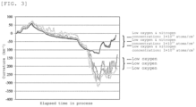
- FIG. 3 is a graph indicating a change in a curvature of the nitride semiconductor wafer during the vapor-phase growth.
- the nitride semiconductor wafer that used the high-resistant low-oxygen CZ silicon substrate with doped nitrogen at 1.0 ⁇ 10 15 atoms/cm 3 caused no plastic deformation during the growth. Warpage after the growth was as small as 30.4 ⁇ m on average.
- Three high-resistant low-oxygen CZ silicon substrates that were same as in Example except that no nitrogen was doped were prepared to epitaxially grow a nitride semiconductor in the same manner as in Example.
Landscapes
- Chemical & Material Sciences (AREA)
- Crystallography & Structural Chemistry (AREA)
- Organic Chemistry (AREA)
- Engineering & Computer Science (AREA)
- Materials Engineering (AREA)
- Metallurgy (AREA)
- Inorganic Chemistry (AREA)
- Chemical Kinetics & Catalysis (AREA)
- General Chemical & Material Sciences (AREA)
- Crystals, And After-Treatments Of Crystals (AREA)
- Recrystallisation Techniques (AREA)
- Chemical Vapour Deposition (AREA)
- Junction Field-Effect Transistors (AREA)
Abstract
Description
- The present invention relates to a nitride semiconductor wafer and a method for producing a nitride semiconductor wafer.
- In high-frequency devices, development to integrate devices such as an antenna, an amplifier, a switch, and a filter is advanced for miniaturization and cost reduction. As higher frequency is used, a circuit becomes more complex, and used materials for the device are various materials including a silicon CMOS (Complementary MOS), a device using a III-V group semiconductor or a nitride semiconductor, and a filter using a piezoelectric material.
- For a substrate to be a base of these devices, a silicon substrate whose large-diameter wafers are inexpensively distributed is considered to be suitable.
-
- Patent Document 1:
JP 2011-103380 A - Patent Document 2:
JP 2020-98839 A - Patent Document 3:
JP 2012-79952 A -
Patent Document 1 discloses growth of a compound semiconductor on a silicon substrate having an oxygen concentration of 0.2×10¹⁸ atoms/cm3 or more. - However, in particular for a substrate for a high-frequency device, a substrate having a low oxygen concentration, which has high resistance and little change in resistivity due to a thermal donor, is considered to be suitable. In addition, the high-frequency device requires to reduce a parasitic capacity of the device, support substrate thereof, and peripheral package in order to improve the high-frequency characteristics. Use of a high-resistant low-oxygen silicon substrate, which hardly generates a thermal donor for the support substrates or the packages, to reduce the parasitic capacity is considered to improve the characteristics and to have a cost merit. As described above, a substrate having a lower oxygen concentration has an advantage in terms of electric characteristics. Such a substrate, however, has a problem of being likely to cause plastic deformation due to the lower oxygen concentration.
- Production of a device includes steps of epitaxial growth on a substrate, a heat treatment, laminating, etc., and during the steps, a stress is generated on the substrate due to difference in a lattice constant or difference in a thermal expansion coefficient between the different materials. Unfortunately, the high-resistant low-oxygen silicon substrate, which has a lower Young's modulus when dislocated than a common low-resistance Czochralski (CZ) silicon substrate produced by the CZ method, has a demerit of being likely to cause plastic deformation. If the plastic deformation occurs, the wafer is largely deformed and fail to return the shape to the original shape, and thereby abnormal warpage or bonding defect may occur.
- Patent Document 2 describes art to grow a nitride semiconductor on a substrate having a high nitrogen concentration and produced by Floating Zone (FZ) method. The FZ method, however, is difficult to obtain a crystal having a high nitrogen concentration in balk, and has a problem of a low yield. In addition, the FZ substrate is difficult to obtain a <111> substrate having a diameter of 200 nm or more, and has a limit of enlarging the diameter.
- Accordingly, the present inventors have focused on the CZ method, which can produce wafers having a large diameter, to earnestly make investigation, and consequently found that a high-resistance CZ silicon substrate with a low-oxygen concentration has deteriorated mechanical properties compared with a low-resistance CZ silicon substrate, leading to a problem of being likely to cause plastic deformation due to dislocation growth. In particular, growth of GaN on a silicon substrate is likely to increase warpage or cause plastic deformation due to a stress derived from difference in a lattice constant or difference in a thermal expansion coefficient. Thus, the stress is reduced with growth condition or a relaxation layer.
- In Patent Document 3, for example, using an intermediate layer of a gallium nitride-based compound semiconductor periodically stacked a plurality of times for relaxing the stress to produce a wafer having little warpage and cracking. However, it is concerned that producing such a complex intermediate layer extends the growth time to decrease flexibility of design.
- The present invention is made to solve the above problem. An object of the present invention is to provide a nitride semiconductor wafer that hardly causes plastic deformation even using a high-resistant low-oxygen silicon single-crystal substrate produced by the CZ method, which is suitably used for a high-frequency device, and that can reduce substrate warpage. An object of the present invention is also to provide a producing method thereof.
- The present invention is made to achieve the above object. The present invention provides a nitride semiconductor wafer, comprising: a silicon single-crystal substrate; and a device layer composed of a nitride semiconductor above the silicon single-crystal substrate, wherein the silicon single-crystal substrate is a CZ silicon single-crystal substrate, and has a resistivity of 1000 Ω·cm or more, an oxygen concentration of 5.0×10¹⁶ atoms/cm3 (JEIDA) or more and 2.0×10¹⁷ atoms/cm3 (JEIDA) or less, and a nitrogen concentration of 5.0×10¹⁴ atoms/cm3 or more.
- Such a nitride semiconductor wafer is a nitride semiconductor wafer with inhibited plastic deformation even using a high-resistant low-oxygen CZ silicon single-crystal substrate, which is suitable for a high-frequency device, and with reduced substrate warpage.
- In addition, such a nitride semiconductor wafer can be a nitride semiconductor wafer using a silicon single-crystal substrate having a larger diameter or many plane orientations.
- In this time, the nitride semiconductor wafer preferably further comprises an intermediate layer composed of a nitride semiconductor or a metal above the silicon single-crystal substrate, wherein the nitride semiconductor wafer has the device layer composed of the nitride semiconductor above the intermediate layer.
- Such an intermediate layer functions as a cushioning layer for improving crystallinity or regulating a stress of the device layer composed of the nitride semiconductor thin film present above the intermediate layer. Thus, such an intermediate layer yields the nitride semiconductor wafer with further inhibited plastic deformation and further reduced substrate warpage.
- The present invention also provides a method for producing a nitride semiconductor wafer, the method comprising a step of epitaxially growing a nitride semiconductor thin film above a silicon single-crystal substrate, wherein used as the silicon single-crystal substrate is a silicon single-crystal substrate produced by a CZ method, having a resistivity of 1000 Ω·cm or more, having an oxygen concentration of 5.0×10¹⁶ atoms/cm3 (JEIDA) or more and 2.0×10¹⁷ atoms/cm3 (JEIDA) or less, and having a nitrogen concentration of 5.0×10¹⁴ atoms/cm3 or more.
- According to such a method for producing a nitride semiconductor wafer, plastic deformation is inhibited even using a high-resistant low-oxygen CZ silicon single-crystal substrate, which is suitable for a high-frequency device, and the nitride semiconductor wafer with reduced substrate warpage can be easily produced.
- In this time, an intermediate layer composed of a nitride semiconductor or a metal is preferably formed above the silicon single-crystal substrate, and the nitride semiconductor thin film is preferably grown above the intermediate layer.
- Such an intermediate layer functions as a cushioning layer for improving crystallinity or regulating a stress of the device layer composed of the nitride semiconductor thin film formed above the intermediate layer. Thus, the nitride semiconductor wafer with further inhibited plastic deformation and reduced substrate warpage can be further easily produced.
- As described above, the inventive nitride semiconductor wafer and the producing method thereof can inhibit plastic deformation even using a high-resistant low-oxygen CZ silicon single-crystal substrate, which is suitable for a high-frequency device, and can reduce substrate warpage.
-
-
FIG. 1 is a schematic sectional view schematically illustrating an example of the inventive nitride semiconductor wafer. -
FIG. 2 is a schematic sectional view illustrating a case of forming a HEMT structure as an application example of the inventive nitride semiconductor wafer. -
FIG. 3 is a graph indicating a change in a curvature of a nitride semiconductor wafer during vapor-phase growth. - As described above, required are a nitride semiconductor wafer and a producing method thereof that hardly cause plastic deformation even using a high-resistant CZ silicon single-crystal substrate, which is suitable for a high-frequency device, and that can reduce substrate warpage.
- The present inventors have earnestly studied the above problem, and consequently found that a nitride semiconductor wafer, comprising: a silicon single-crystal substrate; and a device layer composed of a nitride semiconductor above the silicon single-crystal substrate, wherein the silicon single-crystal substrate is a CZ silicon single-crystal substrate, and has a resistivity of 1000 Ω·cm or more, an oxygen concentration of 5.0×10¹⁶ atoms/cm3 (JEIDA) or more and 2.0×10¹⁷ atoms/cm3 (JEIDA) or less, and a nitrogen concentration of 5.0×10¹⁴ atoms/cm3 or more can provide a nitride semiconductor wafer with inhibited plastic deformation even using a high-resistant low-oxygen CZ silicon single-crystal substrate, which is suitable for a high-frequency device, and with reduced substrate warpage. This finding has led to the completion of the present invention.
- The present inventors have also found that a method for producing a nitride semiconductor wafer, the method comprising a step of epitaxially growing a nitride semiconductor thin film above a silicon single-crystal substrate, wherein used as the silicon single-crystal substrate is a silicon single-crystal substrate produced by a CZ method, having a resistivity of 1000 Ω·cm or more, having an oxygen concentration of 5.0×10¹⁶ atoms/cm3 (JEIDA) or more and 2.0×10¹⁷ atoms/cm3 (JEIDA) or less, and having a nitrogen concentration of 5.0×10¹⁴ atoms/cm3 or more can provide a producing method that can easily produce a nitride semiconductor wafer with inhibited plastic deformation even using a high-resistant low-oxygen CZ silicon single-crystal substrate, which is suitable for a high-frequency device, and with reduced substrate warpage. This finding has led to the completion of the present invention.
- Hereinafter, the present invention will be described in detail with reference to the drawings as an example of an embodiment, but the present invention is not limited thereto.
FIG. 1 illustrates a schematic view of an example of the inventive nitride semiconductor wafer. - A nitride semiconductor wafer 10 according to the present invention illustrated in
FIG. 1 has adevice layer 16 composed of a nitride semiconductor thin film above a silicon single-crystal substrate 12. Used as the silicon single-crystal substrate 12 is a silicon single-crystal substrate produced by the CZ method, and having a resistivity of 1000 Ω·cm or more, an oxygen concentration of 5.0×10¹⁶ atoms/cm3 (JEIDA) or more and 2.0×10¹⁷ atoms/cm3 (JEIDA) or less, and an added (doped) nitrogen at 5.0×10¹⁴ atoms/cm3 or more. - The resistivity is 1000 Ω·cm or more, which is required for a substrate for a high-frequency device. Since a higher resistivity is more preferable, the upper limit is not particularly limited. The resistivity can be, for example, 10 kΩ·cm or less. The oxygen concentration has an upper limit of 2.0×10¹⁷ atoms/cm3 (JEIDA) because a thermal donor non-negligibly affects the resistivity if the oxygen concentration exceeds 2.0×10¹⁷ atoms/cm3 (JEIDA). Since a single crystal having an oxygen concentration of less than 5.0×10¹⁶ atoms/cm3 (JEIDA) is extremely difficult to be produced by the CZ method, the lower limit of the oxygen concentration is 5.0×10¹⁶ atoms/cm3 (JEIDA).
- Unfortunately, reducing the oxygen concentration of the high-resistance substrate as above has a problem of decrease in Young's modulus when dislocated compared with a common low-resistance CZ silicon wafer and is likely to cause plastic deformation. Accordingly, the present inventors have found that using a silicon substrate into which nitrogen is added at 5.0×10¹⁴ atoms/cm3 or more as a high-resistant low-oxygen CZ silicon single-crystal substrate can inhibit the plastic deformation.
- Inhibiting the plastic deformation can reduce abnormal warpage to improve the production yield of the
nitride semiconductor wafer 10. Since the silicon single-crystal substrate 12 can withstand a stress, the nitride semiconductor thin film to be thedevice layer 16 with vapor-phase growth can be thick, resulting in improvement in flexibility of design of the device. In addition, further increasing the nitrogen concentration in the silicon single-crystal substrate 12 to 1.0×10¹⁵ atoms/cm3 or more, particularly 5.0×10¹⁵ atoms/cm3 or more, can further reduce the substrate warpage, and can further certainly prevent the plastic deformation. The concentration of nitrogen contained in the silicon single-crystal substrate 12 is preferably 5.0×10¹⁶ atoms/cm3 or less. This is because the nitrogen concentration of 5.0×10¹⁶ atoms/cm3 or less can prevent decrease in single-crystallization rate of the silicon single crystal, which is a raw material of the silicon single-crystal substrate 12. - In this time, the high-resistant low-oxygen CZ silicon single-crystal substrate preferably has a diameter of 200 mm or more because such a substrate with a large diameter can take the advantage of the CZ method. A plane orientation of the major surface of the substrate is not particularly limited, and can be (100), (110), (111), etc. In particular, a substrate having a diameter of 200 mm or more and a plane orientation of (111) is beneficial because such a substrate is difficult to be produced by the FZ method.
- Such a nitride semiconductor wafer hardly causes the plastic deformation and with reduced warpage even using a high-resistant low-oxygen CZ silicon single-crystal substrate, which is suitable for a high-frequency device.
- As illustrated in
FIG. 1 , the nitride semiconductor wafer may have anintermediate layer 14 between the silicon single-crystal substrate 12 and thedevice layer 16. Theintermediate layer 14 is composed of a nitride semiconductor or a metal. Theintermediate layer 14 serves as an inserted cushioning layer for improving the crystallinity of thedevice layer 16 and regulating the stress. When such improvements in stress and crystallinity are unnecessary, theintermediate layer 14 can be eliminated. With considering a structure of the device, such as a high-frequency filter, theintermediate layer 14 may be produced from a metal usable for a sacrificial layer forming a space or for an electrode. Theintermediate layer 14 may be an intermediate layer composed of a metal, or may be an intermediate layer composed of a nitride semiconductor. When theintermediate layer 14 is composed of a nitride semiconductor, its composition may be different from or same as a composition of the nitride semiconductor thin film to be thedevice layer 16. When theintermediate layer 14 is composed of a nitride semiconductor, it can be mentioned that theintermediate layer 14 and thedevice layer 16 constitute the nitride semiconductor thin film. Theintermediate layer 14 may have the composition changed during the growth. - On a surface of the silicon single-crystal substrate 12 (boundary with the
intermediate layer 14 inFIG. 1 ), a trap-rich layer that shortens a life of the carrier may be formed. - As an application example of the inventive nitride semiconductor wafer,
FIG. 2 illustrates a case of forming a high electron-mobility transistor (HEMT) structure. In the high electron-mobility transistor (HEMT) structure as illustrated inFIG. 2 , thedevice layer 16 is constituted with a gallium nitride (GaN)layer 17 and anelectron supply layer 18 composed of AlGaN formed thereon, for example. - Gallium nitride has a difference in a lattice constant of 17% and a difference in a thermal expansion coefficient of 116% with the Si (111) single crystal. Thus, a stress is applied to the thin film and the substrate during the growth at high temperature. In addition, since the gallium nitride with growing is heated at 1000°C or higher, a stress applied to the wafer does not cause brittle fracture but exhibits ductility, which generates dislocation to cause the plastic deformation.
- Accordingly, in the present invention, the silicon substrate into which nitrogen is added at 5.0×10¹⁴ atoms/cm3 or more is used as the silicon single-
crystal substrate 12 to prevent progress of the dislocation of the silicon single-crystal substrate 12, which can prevent the plastic deformation. Preventing the plastic deformation can reduce abnormal warpage to improve the production yield of thenitride semiconductor wafer 10. Since the silicon single-crystal substrate 12 can withstand a stress, the nitride semiconductor thin film to be thedevice layer 16 with vapor-phase growth can be thick, resulting in improvement in flexibility of design of the device. - Next, the inventive method for producing a nitride semiconductor wafer will be described. The description will be made with reference to
FIG. 1 . In the inventive method for producing a nitride semiconductor wafer, the silicon single-crystal substrate 12 is first prepared, and then the nitride semiconductor thin film to be thedevice layer 16 is epitaxially grown above the silicon single-crystal substrate 12. In the present invention, used as the silicon single-crystal substrate 12 is a silicon single-crystal substrate produced by a CZ method, having an oxygen concentration of 5.0×10¹⁶ atoms/cm3 (JEIDA) or more and 2.0×10¹⁷ atoms/cm3 (JEIDA) or less, having a nitrogen concentration of 5.0×10¹⁴ atoms/cm3 or more, and having a resistivity of 1000 Ω·cm or more. - Before the growth of the nitride semiconductor thin film to be the
device layer 16, theintermediate layer 14 may be formed above the silicon single-crystal substrate 12 and the nitride semiconductor thin film to be thedevice layer 16 may be grown above theintermediate layer 14. - When the trap-rich layer is formed on the surface of the silicon single-crystal substrate 12 (boundary with the
intermediate layer 14 inFIG. 1 ), a forming method thereof is not particularly limited. The trap-rich layer can be formed by ion injection or irradiation of ionizing radiation, such as electron beam, X-ray, and γ-ray. - The
device layer 16 composed of the nitride semiconductor thin film is produced by vapor growth, such as a thermal CVD (chemical vapor deposition) method, a MOVPE (metalorganic vapor phase epitaxy) method, an MBE (molecular beam epitaxy) method, a vacuum deposition method, and a sputtering method, above the silicon single-crystal substrate 12 (above theintermediate layer 14 when theintermediate layer 14 is formed above the silicon single-crystal substrate 12). As the device layer, III-V group semiconductors can be used in addition to the nitride semiconductor thin film, such as, for example, GaN, AlN, InN, AlGaN, InGaN, AlInN, and AlScN. The nitride semiconductor thin film can have a thickness of 1 to 10 µm, and can be designed depending on the device. - In the high electron-mobility transistor (HEMT) structure illustrated in
FIG. 2 , thedevice layer 16 is desirably a crystal having few crystalline defects and little impurity such as carbon and oxygen for improving device characteristics. Such a crystal can be produced by using a MOVPE method at 900°C to 1350°C. - Hereinafter, the present invention will be specifically described with Example, but the present invention is not limited thereto.
- Three high-resistant low-oxygen CZ silicon substrates produced by the CZ method and having a diameter of 150 mm were prepared. The silicon single-crystal substrates had a resistivity of 1000 Ω·cm or more, an oxygen concentration of 5.0×10¹⁶ to 2.0×10¹⁷ atoms/cm3 (JEIDA), and doped nitrogen. The concentration of the doped nitrogen was 1.0×10¹⁵ atoms/cm3. A nitride semiconductor was epitaxially grown on the prepared high-resistant low-oxygen CZ silicon substrate by using a MOVPE furnace. The growth temperature was 1200°C, and an epitaxial layer having a total thickness of 2.8 µm was grown.
-
FIG. 3 is a graph indicating a change in a curvature of the nitride semiconductor wafer during the vapor-phase growth. The nitride semiconductor wafer that used the high-resistant low-oxygen CZ silicon substrate with doped nitrogen at 1.0×10¹⁵ atoms/cm3 caused no plastic deformation during the growth. Warpage after the growth was as small as 30.4 µm on average. - Three high-resistant low-oxygen CZ silicon substrates that were same as in Example except that no nitrogen was doped were prepared to epitaxially grow a nitride semiconductor in the same manner as in Example.
- As indicated in
FIG. 3 , all the three of the three nitride semiconductor wafers that used the high-resistant low-oxygen CZ silicon substrate without nitrogen doping caused plastic deformation. On the nitride semiconductor wafer that used the high-resistant low-oxygen CZ silicon substrate without nitrogen doping, warpage after the growth was as large as 174.1 µm on average, which was a defect. - From Example and Comparative Example, it has been found that the nitrogen concentration in the silicon single-
crystal substrate 12 of 5.0×10¹⁴ atoms/cm3 or more can yield the effect of the present invention of inhibiting plastic deformation occurrence to reduce substrate warpage. - It should be noted that the present invention is not limited to the above-described embodiments. The embodiments are just examples, and any examples that have substantially the same feature and demonstrate the same functions and effects as those in the technical concept disclosed in claims of the present invention are included in the technical scope of the present invention.
Claims (4)
- A nitride semiconductor wafer, comprising:a silicon single-crystal substrate; anda device layer composed of a nitride semiconductor above the silicon single-crystal substrate,wherein the silicon single-crystal substrate is a CZ silicon single-crystal substrate, and has a resistivity of 1000 Ω·cm or more, an oxygen concentration of 5.0×10¹⁶ atoms/cm3 (JEIDA) or more and 2.0×10¹⁷ atoms/cm3 (JEIDA) or less, and a nitrogen concentration of 5.0×10¹⁴ atoms/cm3 or more.
- The nitride semiconductor wafer according to claim 1, further comprising an intermediate layer composed of a nitride semiconductor or a metal above the silicon single-crystal substrate, wherein the nitride semiconductor wafer has the device layer composed of the nitride semiconductor above the intermediate layer.
- A method for producing a nitride semiconductor wafer, the method comprising a step of epitaxially growing a nitride semiconductor thin film above a silicon single-crystal substrate, wherein used as the silicon single-crystal substrate is a silicon single-crystal substrate produced by a CZ method, having a resistivity of 1000 Ω·cm or more, having an oxygen concentration of 5.0×10¹⁶ atoms/cm3 (JEIDA) or more and 2.0×10¹⁷ atoms/cm3 (JEIDA) or less, and having a nitrogen concentration of 5.0×10¹⁴ atoms/cm3 or more.
- The method for producing a nitride semiconductor wafer according to claim 3, wherein an intermediate layer composed of a nitride semiconductor or a metal is formed above the silicon single-crystal substrate, and the nitride semiconductor thin film is grown above the intermediate layer.
Applications Claiming Priority (2)
| Application Number | Priority Date | Filing Date | Title |
|---|---|---|---|
| JP2020128377A JP6866952B1 (en) | 2020-07-29 | 2020-07-29 | Nitride semiconductor wafer and method for manufacturing nitride semiconductor wafer |
| PCT/JP2021/026066 WO2022024729A1 (en) | 2020-07-29 | 2021-07-12 | Nitride semiconductor wafer and method for producing nitride semiconductor wafer |
Publications (2)
| Publication Number | Publication Date |
|---|---|
| EP4191639A1 true EP4191639A1 (en) | 2023-06-07 |
| EP4191639A4 EP4191639A4 (en) | 2024-09-11 |
Family
ID=75638913
Family Applications (1)
| Application Number | Title | Priority Date | Filing Date |
|---|---|---|---|
| EP21850368.8A Pending EP4191639A4 (en) | 2020-07-29 | 2021-07-12 | NITRIDE SEMICONDUCTOR WAFER AND METHOD FOR PRODUCING A NITRIDE SEMICONDUCTOR WAFER |
Country Status (6)
| Country | Link |
|---|---|
| US (1) | US12610599B2 (en) |
| EP (1) | EP4191639A4 (en) |
| JP (1) | JP6866952B1 (en) |
| CN (1) | CN115997271A (en) |
| TW (1) | TWI894315B (en) |
| WO (1) | WO2022024729A1 (en) |
Families Citing this family (3)
| Publication number | Priority date | Publication date | Assignee | Title |
|---|---|---|---|---|
| EP4202088A4 (en) * | 2020-08-18 | 2024-09-25 | Shin-Etsu Handotai Co., Ltd. | Method for manufacturing nitride semiconductor wafer, and nitride semiconductor wafer |
| JP7487726B2 (en) | 2021-11-30 | 2024-05-21 | 信越半導体株式会社 | Nitride semiconductor substrate and method for producing same |
| JP2024172767A (en) | 2023-06-01 | 2024-12-12 | 信越半導体株式会社 | METHOD FOR MANUFACTURING NITRIDE SEMICONDUCTOR SUBSTRATE, METHOD FOR MANUFACTURING HYBRID IC, AND NITRIDE SEMICONDUCTOR SUBSTRATE |
Family Cites Families (8)
| Publication number | Priority date | Publication date | Assignee | Title |
|---|---|---|---|---|
| DE19983188T1 (en) * | 1998-05-01 | 2001-05-10 | Nippon Steel Corp | Silicon semiconductor substrate and method for its production |
| KR100749935B1 (en) | 2004-11-16 | 2007-08-16 | 주식회사 실트론 | Silicon Monocrystalline and Silicon Wafers |
| US8263484B2 (en) * | 2009-03-03 | 2012-09-11 | Sumco Corporation | High resistivity silicon wafer and method for manufacturing the same |
| JP5636183B2 (en) * | 2009-11-11 | 2014-12-03 | コバレントマテリアル株式会社 | Compound semiconductor substrate |
| JP5159858B2 (en) * | 2010-09-08 | 2013-03-13 | コバレントマテリアル株式会社 | Gallium nitride compound semiconductor substrate and manufacturing method thereof |
| JP6044277B2 (en) * | 2012-11-08 | 2016-12-14 | 信越半導体株式会社 | Manufacturing method of silicon single crystal wafer |
| US10644142B2 (en) * | 2017-12-22 | 2020-05-05 | Nxp Usa, Inc. | Semiconductor devices with doped regions functioning as enhanced resistivity regions or diffusion barriers, and methods of fabrication therefor |
| JP2020098839A (en) | 2018-12-17 | 2020-06-25 | 信越半導体株式会社 | Nitride semiconductor wafer manufacturing method and nitride semiconductor wafer |
-
2020
- 2020-07-29 JP JP2020128377A patent/JP6866952B1/en active Active
-
2021
- 2021-07-12 US US18/013,618 patent/US12610599B2/en active Active
- 2021-07-12 EP EP21850368.8A patent/EP4191639A4/en active Pending
- 2021-07-12 CN CN202180045965.0A patent/CN115997271A/en active Pending
- 2021-07-12 WO PCT/JP2021/026066 patent/WO2022024729A1/en not_active Ceased
- 2021-07-19 TW TW110126343A patent/TWI894315B/en active
Also Published As
| Publication number | Publication date |
|---|---|
| JP2022025512A (en) | 2022-02-10 |
| JP6866952B1 (en) | 2021-04-28 |
| TW202206656A (en) | 2022-02-16 |
| CN115997271A (en) | 2023-04-21 |
| US12610599B2 (en) | 2026-04-21 |
| EP4191639A4 (en) | 2024-09-11 |
| WO2022024729A1 (en) | 2022-02-03 |
| US20230290835A1 (en) | 2023-09-14 |
| TWI894315B (en) | 2025-08-21 |
Similar Documents
| Publication | Publication Date | Title |
|---|---|---|
| JP4469396B2 (en) | Silicon carbide single crystal ingot, substrate obtained therefrom and epitaxial wafer | |
| US12610599B2 (en) | Nitride semiconductor wafer and method for producing nitride semiconductor wafer | |
| EP4012750A1 (en) | Substrate for electronic device and production method therefor | |
| EP3998376A1 (en) | Substrate for electronic device and production method therefor | |
| JP2020098839A (en) | Nitride semiconductor wafer manufacturing method and nitride semiconductor wafer | |
| EP1972702A1 (en) | Method for manufacturing aluminum nitride crystal, aluminum nitride crystal, aluminum nitride crystal substrate and semiconductor device | |
| JP7142184B2 (en) | Nitride semiconductor wafer manufacturing method and nitride semiconductor wafer | |
| US12606935B2 (en) | Silicon single crystal substrate for vapor phase growth, vapor phase growth substrate and methods for producing them | |
| JP5162895B2 (en) | Aluminum nitride crystal manufacturing method, aluminum nitride crystal, aluminum nitride crystal substrate, and semiconductor device | |
| EP4442868A1 (en) | Nitride semiconductor substrate and method for producing same | |
| US20240371628A1 (en) | Method for manufacturing nitride semiconductor substrate | |
| EP4462465A1 (en) | Nitride semiconductor substrate and method for producing same | |
| CN116798856B (en) | Preparation method and structure of SiC-based GaN epitaxial structure, preparation method of HBT and HBT | |
| EP4411032A1 (en) | Nitride semiconductor wafer production method and nitride semiconductor wafer | |
| US20110215439A1 (en) | Epitaxial growth substrate, manufacturing method thereof, nitride-based compound semiconductor substrate, and nitride-based compound semiconductor self-supporting substrate |
Legal Events
| Date | Code | Title | Description |
|---|---|---|---|
| STAA | Information on the status of an ep patent application or granted ep patent |
Free format text: STATUS: THE INTERNATIONAL PUBLICATION HAS BEEN MADE |
|
| PUAI | Public reference made under article 153(3) epc to a published international application that has entered the european phase |
Free format text: ORIGINAL CODE: 0009012 |
|
| STAA | Information on the status of an ep patent application or granted ep patent |
Free format text: STATUS: REQUEST FOR EXAMINATION WAS MADE |
|
| 17P | Request for examination filed |
Effective date: 20221228 |
|
| AK | Designated contracting states |
Kind code of ref document: A1 Designated state(s): AL AT BE BG CH CY CZ DE DK EE ES FI FR GB GR HR HU IE IS IT LI LT LU LV MC MK MT NL NO PL PT RO RS SE SI SK SM TR |
|
| DAV | Request for validation of the european patent (deleted) | ||
| DAX | Request for extension of the european patent (deleted) | ||
| A4 | Supplementary search report drawn up and despatched |
Effective date: 20240808 |
|
| RIC1 | Information provided on ipc code assigned before grant |
Ipc: C30B 25/18 20060101ALI20240802BHEP Ipc: C30B 29/40 20060101ALI20240802BHEP Ipc: C30B 29/06 20060101ALI20240802BHEP Ipc: H01L 21/02 20060101AFI20240802BHEP |