EP4186700A1 - Light irradiation device - Google Patents
Light irradiation device Download PDFInfo
- Publication number
- EP4186700A1 EP4186700A1 EP21846386.7A EP21846386A EP4186700A1 EP 4186700 A1 EP4186700 A1 EP 4186700A1 EP 21846386 A EP21846386 A EP 21846386A EP 4186700 A1 EP4186700 A1 EP 4186700A1
- Authority
- EP
- European Patent Office
- Prior art keywords
- light
- cover glass
- irradiation device
- reflective
- reflective mirror
- Prior art date
- Legal status (The legal status is an assumption and is not a legal conclusion. Google has not performed a legal analysis and makes no representation as to the accuracy of the status listed.)
- Granted
Links
Images


Classifications
-
- B—PERFORMING OPERATIONS; TRANSPORTING
- B41—PRINTING; LINING MACHINES; TYPEWRITERS; STAMPS
- B41J—TYPEWRITERS; SELECTIVE PRINTING MECHANISMS, i.e. MECHANISMS PRINTING OTHERWISE THAN FROM A FORME; CORRECTION OF TYPOGRAPHICAL ERRORS
- B41J11/00—Devices or arrangements of selective printing mechanisms, e.g. ink-jet printers or thermal printers, for supporting or handling copy material in sheet or web form
- B41J11/0015—Devices or arrangements of selective printing mechanisms, e.g. ink-jet printers or thermal printers, for supporting or handling copy material in sheet or web form for treating before, during or after printing or for uniform coating or laminating the copy material before or after printing
- B41J11/002—Curing or drying the ink on the copy materials, e.g. by heating or irradiating
- B41J11/0021—Curing or drying the ink on the copy materials, e.g. by heating or irradiating using irradiation
- B41J11/00218—Constructional details of the irradiation means, e.g. radiation source attached to reciprocating print head assembly or shutter means provided on the radiation source
-
- B—PERFORMING OPERATIONS; TRANSPORTING
- B41—PRINTING; LINING MACHINES; TYPEWRITERS; STAMPS
- B41J—TYPEWRITERS; SELECTIVE PRINTING MECHANISMS, i.e. MECHANISMS PRINTING OTHERWISE THAN FROM A FORME; CORRECTION OF TYPOGRAPHICAL ERRORS
- B41J11/00—Devices or arrangements of selective printing mechanisms, e.g. ink-jet printers or thermal printers, for supporting or handling copy material in sheet or web form
- B41J11/0015—Devices or arrangements of selective printing mechanisms, e.g. ink-jet printers or thermal printers, for supporting or handling copy material in sheet or web form for treating before, during or after printing or for uniform coating or laminating the copy material before or after printing
- B41J11/002—Curing or drying the ink on the copy materials, e.g. by heating or irradiating
- B41J11/0021—Curing or drying the ink on the copy materials, e.g. by heating or irradiating using irradiation
- B41J11/00214—Curing or drying the ink on the copy materials, e.g. by heating or irradiating using irradiation using UV radiation
-
- B—PERFORMING OPERATIONS; TRANSPORTING
- B41—PRINTING; LINING MACHINES; TYPEWRITERS; STAMPS
- B41F—PRINTING MACHINES OR PRESSES
- B41F23/00—Devices for treating the surfaces of sheets, webs, or other articles in connection with printing
- B41F23/04—Devices for treating the surfaces of sheets, webs, or other articles in connection with printing by heat drying, by cooling, by applying powders
Definitions
- the present invention relates to a light irradiation device that irradiates an irradiation object with light when the irradiation object is transferred in one direction.
- a printing device that performs a printing process using UV ink that is cured by being irradiated with ultraviolet rays.
- the printing device discharges ink from a nozzle of a head toward a medium and emits ultraviolet rays to dots formed on the medium.
- the dots are fixed on the medium as the dots are cured by being irradiated with ultraviolet rays, such that a smooth printing process may be performed even on a medium that hardly absorbs a liquid.
- an ultraviolet irradiation device used for such a printing device practically uses a light-emitting diode (LED) element as a light source, instead of the existing discharge lamp, to meet the needs for a reduction in power consumption, a prolonged lifespan, and a compact size of the device (e.g., Patent Document 1).
- LED light-emitting diode
- Patent Document 1 Japanese Patent No. 5482537
- the ultraviolet irradiation device disclosed in Patent Document 1 has a light source unit having a plurality of ultraviolet ray light sources (ultraviolet ray LEDs) arranged in a direction perpendicular to a transfer direction of an irradiation object, and a pair of reflective members disposed between the light source unit and the irradiation object so that the light source unit is fitted with the pair of reflective members from upstream and downstream sides based on the transfer direction.
- the ultraviolet irradiation device adopts a configuration that provides directionality to ultraviolet rays by guiding the ultraviolet rays from an ultraviolet ray source to a pair of reflective plates and emitting the ultraviolet rays.
- the light amount (intensity) of the ultraviolet rays decreases each time the ultraviolet rays are reflected by the reflective members, because the reflective members have predetermined reflectance. For this reason, it is necessary to increase the number of ultraviolet LEDs to supplement the light amount by the amount of decrease in light amount in order to obtain a predetermined light amount on the irradiation object (i.e., the light amount for assuredly curing the UV ink). Further, as a result, there occurs a problem in that the cost, size, and power consumption of the device are increased. Accordingly, there is a need for a light irradiation device capable of performing efficient irradiation without increasing the number of LEDs.
- the present invention has been contrived in consideration of the above-mentioned problems in the related art, and an object of the present invention is to provide a light irradiation device capable of performing efficient irradiation while providing directionality to exiting light.
- a light irradiation device of the present invention emits rays to an irradiation object capable of relatively moving in a first direction and includes: a substrate defined in the first direction and a second direction perpendicular to the first direction; a plurality of light-emitting elements arranged on the substrate so that the number of light-emitting elements in the second direction is n (n is two or more integers) and the light-emitting elements are arranged in m (m is two or more integers) rows in the first direction, the plurality of light-emitting elements being disposed so that directions of optical axes thereof are aligned with a third direction orthogonal to the first direction and the second direction; a cover glass configured to transmit the rays emitted from the plurality of light-emitting elements; a support part configured to support the cover glass and having an opening portion through which the rays having passed through the cover glass passes; and a pair of first reflective mirrors disposed between the substrate
- the first reflective surfaces 108a and 109a may provide directionality to the exiting light and perform efficient irradiation.
- the light irradiation device may include a second reflective mirror extending to an upstream side based on the first direction from a tip portion of the first reflective mirror positioned at the upstream side based on the first direction so as to face the cover glass, the second reflective mirror being configured to reflect the rays, which have been reflected by the irradiation object, to the irradiation object.
- the second reflective mirror may be integrated with the first reflective mirror positioned at the upstream side based on the first direction.
- the light irradiation device may include a third reflective mirror extending to a downstream side based on the first direction from a tip portion of the first reflective mirror positioned at the downstream side based on the first direction so as to face the cover glass, the third reflective mirror being configured to reflect the rays, which have been reflected by the irradiation object, to the irradiation object.
- the third reflective mirror may be integrated with the first reflective mirror positioned at the downstream side based on the first direction.
- the light irradiation device may include a housing configured to accommodate the substrate, the plurality of light-emitting elements, and the pair of first reflective mirrors, and the support part and the cover glass may constitute a part of the housing.
- the ray may be a ray in an ultraviolet wavelength region.
- the irradiation object may have a sheet shape, and the ray in the ultraviolet wavelength region may cure ink applied onto a surface of the irradiation object.
- the light irradiation device capable of performing efficient irradiation while providing directionality to exiting light.
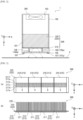
- FIGS. 1 and 2 are views illustrating a configuration of a light irradiation device 1 according to a first embodiment of the present invention.
- FIG. 1(a) is a perspective view
- FIG. 1(b) is a front view
- FIG. 2 is a cross-sectional view taken along line A-A in FIG. 1(b) .
- the light irradiation device 1 according to the present embodiment refers to a light source device embedded in a printing device or the like and configured to cure ultraviolet curable ink or ultraviolet curable resin.
- the light irradiation device 1 is disposed above an irradiation object P (e.g., a sheet-shaped recording medium or the like) transferred in one direction and emits line-shaped ultraviolet rays to the irradiation object P.
- FIG. 1(a) illustrates only the light irradiation device 1 for convenience of description. However, in an actual printing device or the like, a plurality of recording heads for providing ink with different colors is arranged in a transfer direction of the irradiation object P, and the light irradiation device 1 is disposed in a narrow space at a downstream side of the recording heads.
- the transfer direction of the irradiation object P is defined and described as an X-axis direction (first direction)
- an arrangement direction of light-emitting diode (LED) elements 217 to be described below is defined and described as a Y-axis direction (second direction)
- a direction in which the LED elements 217 emit ultraviolet rays is defined and described as a Z-axis direction (third direction).
- the ultraviolet ray is considered as meaning light having a wavelength of 400 nm or less.
- the ultraviolet ray means light having a wavelength (e.g., a wavelength of 250 to 420 nm) capable of curing the ultraviolet curable ink applied onto the irradiation object P.
- the present embodiment describes a light irradiation device 1 that includes a light source unit 200, cooling fans 300, and a housing 100 configured to accommodate the light source unit 200 and the cooling fans 300.
- the housing 100 is a casing having a box shape elongated in the Y-axis direction, and a cover glass 105 made of glass is provided on a front surface (a surface based on the plus Z-axis direction) of the housing 100 and configured such that the ultraviolet rays exit the cover glass 105.
- a pair of mirror units 108 and 109 is disposed between the light source unit 200 and the cover glass 105 and spaced apart from each other in the X-axis direction ( FIG. 2 ).
- a support plate 107 (support part) is disposed on the front surface of the cover glass 105 and supports a rim portion of the cover glass 105 from a side based on the plus Z-axis direction ( FIGS. 1(b) and 2 ).
- the support plate 107 has a rectangular opening 107a (opening portion) formed at a central portion thereof.
- the ultraviolet rays passing through the cover glass 105 are emitted to the irradiation object P through the opening 107a.
- the cover glass 105 and the support plate 107 are disposed to cover the front surface of the housing 100, and the cover glass 105 and the support plate 107 constitute a part of the housing 100.
- an exhaust port 101 for discharging air in the housing 100 is formed in a left surface (a surface based on the minus X-axis direction) of the housing 100.
- Four intake ports 103 for supplying air into the housing 100 are formed in a rear surface (a surface based on the minus Z-axis direction) of the housing 100, and the cooling fans 300 are disposed to respectively correspond to the intake ports 103 ( FIGS. 1(a) and 2 ).
- the light irradiation device 1 is electrically connected to a power source device (not illustrated), and electric power is supplied from the power source device to the light source unit 200, the cooling fans 300, and the like.
- FIG. 3 is a view for explaining a configuration of the light source unit 200 of the present embodiment
- FIG. 3(a) is a front view (a view viewed from a side based on the plus Z-axis direction)
- FIG. 3(b) is a side view (a view viewed from a side based on the minus X-axis direction).
- the light source unit 200 includes four LED modules 210 disposed side by side in the Y-axis direction, and a heat sink 220.
- the ultraviolet rays emitted from the LED modules 210 are guided by the pair of mirror units 108 and 109 and emitted to the irradiation object P through the opening 107a and the cover glass 105 disposed on the front surface of the housing 100 (see broken-line arrows in FIG. 2 ).
- the LED module 210 includes a substrate 215 having a rectangular plate shape defined in the X-axis direction and the Y-axis direction, and the plurality of LED elements 217 having the same properties.
- the LED module 210 is fixed to an end surface (an end surface based on the plus Z-axis direction) of a base plate 222 of the heat sink 220.
- the substrate 215 of each of the LED modules 210 is a rectangular wiring substrate made of a material (e.g., aluminum nitride) having high thermal conductivity.
- the LED elements 217 of 5 rows (X-axis direction) ⁇ 20 (Y-axis direction) are mounted on the surface of the substrate in a chip-on-board (COB) manner.
- the LED elements 217 are disposed in an LED mounting region S (a region surrounded by a broken line in FIG. 3(a) ) of an approximately central portion of the substrate 215 based on the X-axis direction.
- the LED elements 217 are disposed at predetermined intervals (e.g., 2 mm) in the X-axis direction and the Y-axis direction.
- the LED elements 217 disposed in the respective rows are sequentially referred to as LED elements 217a, 217b, 217c, 217d, and 217e in the X-axis direction.
- An anode pattern (not illustrated) and a cathode pattern (not illustrated) are formed on the substrate 215 to supply electric power to each of the LED elements 217.
- Each of the LED elements 217 is electrically connected to the anode pattern and the cathode pattern by soldering.
- the substrate 215 is electrically connected to a non-illustrated driver circuit by means of a non-illustrated wire cable, and each of the LED elements 217 is configured to be supplied with a drive current from the driver circuit through the anode pattern and the cathode pattern.
- the ultraviolet rays (e.g., wavelength of 385 nm) corresponding in light amount to the drive current are emitted from each of the LED element 217.
- the line-shaped ultraviolet rays parallel to the Y-axis direction are emitted from the LED module 210.
- the four LED modules 210 are arranged in the Y-axis direction, and the line-shaped ultraviolet rays from the respective LED modules 210 are continued in the Y-axis direction.
- each of the LED elements 217 is adjusted so that each of the LED elements 217 of the present embodiment emits the ultraviolet rays with approximately uniform light amount, and the line-shaped ultraviolet rays emitted from the four LED modules 210 have approximately uniform light amount distributions in the X-axis direction and the Y-axis direction.
- the heat sink 220 refers to a kind of an air-cooled heat sink disposed to be in close contact with a back surface of the substrate 215 of the LED module 210 and configured to dissipate heat generated by each of the LED modules 210.
- the heat sink 220 is made of a material such as aluminum or copper having good thermal conductivity and includes the base plate 222 having a thin-plate shape extending in the Y-axis direction, and a plurality of heat radiating fins 225 formed on a surface of the heat sink 220 opposite to the surface being in contact with the substrate 215.
- the heat radiating fins 225 each have a thin-plate shape parallel to the X-Z plane and disposed at predetermined intervals in the Y-axis direction.
- cooling air produced by the cooling fans 300 uniformly cools the plurality of heat radiating fins 225.
- the respective LED modules 210 are uniformly cooled by the heat sink 220 and the cooling fans 300, which inhibits a deterioration in luminous efficiency caused by an increase in temperature of the LED elements 217.
- the pair of mirror units 108 and 109 is disposed between the light source unit 200 and the cover glass 105 and spaced apart from each other in the X-axis direction ( FIG. 2 ).
- the support plate 107 (support part) is disposed on the front surface of the cover glass 105 and supports the rim portion of the cover glass 105 from the side based on the plus Z-axis direction ( FIGS. 1(b) and 2 ).
- the pair of mirror units 108 and 109 are each a metallic plate-shaped member extending in the Y-axis direction so that the optical paths of the respective ultraviolet rays emitted from the LED elements 217 are interposed therebetween in the X-axis direction.
- the mirror units 108 and 109 extend in the Z-axis direction so as to be disposed uprightly and approximately perpendicularly to the cover glass 105 and disposed symmetrically so that the optical paths of the ultraviolet rays emitted from the LED elements 217 are interposed between the mirror units 108 and 109.
- the mirror units 108 and 109 respectively have first reflective surfaces 108a and 109a facing each other so that the optical paths of the ultraviolet rays emitted from the LED elements 217 are interposed therebetween.
- the ultraviolet ray emitted from the LED element 217 has been known as being dispersed at a predetermined diffusion angle and decreased in intensity when the ultraviolet ray has a large angle component.
- the first reflective surfaces 108a and 109a are disposed so that the optical paths of the ultraviolet rays emitted from the LED elements 217 are interposed therebetween, the ultraviolet rays, which include even the ultraviolet rays having low intensity and a large angle component, are guided by the first reflective surfaces 108a and 109a and exit through the cover glass 105.
- the light amount decreases each time the ultraviolet rays are reflected by the first reflective surfaces 108a and 109a because the first reflective surfaces 108a and 109a have predetermined reflectance (e.g., 90%).
- predetermined reflectance e.g. 90%
- the ultraviolet ray which has a small angle component (e.g., the ultraviolet ray with a diffusion angle of ⁇ 60°) among the ultraviolet rays emitted from the LED elements 217, exits after being reflected by the first reflective surfaces 108a and 109a once or without being reflected, and the ultraviolet ray, which has a large angle component (e.g., the ultraviolet ray with a diffusion angle of > 60°), exits after being reflected by the first reflective surfaces 108a and 109a one or more times (details will be described below).
- a small angle component e.g., the ultraviolet ray with a diffusion angle of ⁇ 60°
- FIG. 4 is a schematic view for explaining a relationship between the arrangement of the LED module 210, the mirror units 108 and 109, the cover glass 105, and the support plate 107 and the rays emitted from the respective LED elements 217.
- FIG. 4(a) is a view illustrating a relationship with the ultraviolet ray having a small diffusion angle (e.g., a diffusion angle of ⁇ 60°)
- FIG. 4(b) is a view illustrating a relationship with the ultraviolet ray having a large diffusion angle (e.g., a diffusion angle of > 60°).
- a small diffusion angle e.g., a diffusion angle of ⁇ 60°
- FIG. 4(b) is a view illustrating a relationship with the ultraviolet ray having a large diffusion angle (e.g., a diffusion angle of > 60°).
- L60a represents the ray having a diffusion angle of 60° and emitted from the LED element 217a
- L60c represents the ray having a diffusion angle of 60° and emitted from the LED element 217c
- L60e represents the ray having a diffusion angle of 60° and emitted from the LED element 217e
- L0a represents the ray having a diffusion angle of 0° and emitted from the LED element 217a
- L65a represents the ray having a diffusion angle of 65° and emitted from the LED element 217a
- L80e represents the ray having a diffusion angle of 80° and emitted from the LED element 217e.
- each of the LED elements 217 has a rectangular shape.
- each of the LED elements 217 is sufficiently thin in the Z-axis direction, and a light-emitting point of each of the LED elements 217 is substantially disposed on the surface of the substrate 215.
- the ray L60a which has a diffusion angle of 60° among the ultraviolet rays emitted from the LED element 217a, is reflected by the first reflective surface 108a once and exits through the cover glass 105.
- the ray L60a exits through the cover glass 105 without entering the first reflective surface 109a (i.e., not passing through a tip of the first reflective surface 109a) ( FIG. 4(a) ).
- the ray L60c which has a diffusion angle of 60° among the ultraviolet rays emitted from the LED element 217c, is reflected by the first reflective surfaces 108a and 109a once and exits through the cover glass 105.
- the ray L60e which has a diffusion angle of 60° among the ultraviolet rays emitted from the LED element 217e, is reflected by the first reflective surface 109a once and exits through the cover glass 105.
- the ray L60e exits through the cover glass 105 without entering the first reflective surface 108a (i.e., not passing through a tip of the first reflective surface 108a).
- the ray which has a diffusion angle smaller than 60° among the ultraviolet rays emitted from the respective LED elements 217, also exits through the cover glass 105 after being reflected by the first reflective surfaces 108a and 109a once or without being reflected.
- the ray (the ray L60a, L60c, L60e, or L0a), which has a diffusion angle of 60° or less, passes through the cover glass 105 and then reaches the irradiation object P after passing through the opening 107a (i.e., without being vignetted by the support plate 107).
- the ray i.e., the ray L65a having a diffusion angle of 65° or the ray L80e having a diffusion angle of 80°
- the first reflective surfaces 108a and 109a one or more times and exits through the cover glass 105 ( FIG. 4(b) ).
- some rays e.g., the rays L65a
- the rays L65a each having a diffusion angle larger than 60° pass through the cover glass 105 and the opening 107a (i.e., without being vignetted by the support plate 107) and then reach the irradiation object P
- the other rays e.g., the rays L80e
- the component such as the support plate 107 without passing through the opening 107a (i.e., while being vignetted by the support plate 107) and then reach the irradiation object P.
- a distance in the X-axis direction from a central axis (a light-emitting point) of the LED element 217a to the first reflective surface 109a may be represented by ⁇ 3h from the relationship with the ray L60a.
- a distance in the X-axis direction from a central axis (a light-emitting point) of the LED element 217e to the first reflective surface 108a may be represented by ⁇ 3h from the relationship with the ray L60e. Therefore, an interval b between the first reflective surfaces 108a and 109a may be represented by b ⁇ ⁇ 3 h + ⁇ 3 h ⁇ a .
- Expression 1 may be obtained by modifying the above-mentioned expression.
- a distance in the X-axis direction from the central axis (the light-emitting point) of the LED element 217a to one end (an end based on the plus X-axis direction) of the support plate 107 may be represented by ⁇ 3d from the relationship with the ray L60a.
- a distance in the X-axis direction from the central axis (the light-emitting point) of the LED element 217e to the other end (the end based on the minus X-axis direction) of the support plate 107 may be represented by V3d from the relationship with the ray L60e. Therefore, an interval w of the support plate 107 in the X-axis direction may be represented by w ⁇ ⁇ 3 d + ⁇ 3 d ⁇ a .
- Expression 2 may be obtained by modifying the above-mentioned expression.
- the ray (ultraviolet ray) having high intensity and the diffusion angle of 60° or less reaches the irradiation object P while being reflected by the first reflective surfaces 108a and 109a once or without being reflected, the influence made by the reflection by the first reflective surfaces 108a and 109a (i.e., a decrease in light amount) is inhibited.
- the ray (ultraviolet ray) having the diffusion angle larger than 60° is reflected by the first reflective surfaces 108a and 109a one or more times, but the influence of the overall amount of light emitted to the irradiation object P is small (i.e., the influence of the decrease in light amount is small) because the ray (ultraviolet ray) having the diffusion angle larger than 60° has low intensity.
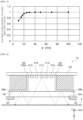
- FIG. 5 illustrates a simulation result for explaining an operational effect of the light irradiation device 1 of the present embodiment.
- the horizontal axis indicates an interval between the support plates 107 in the X-axis direction (i.e., a width w (mm) of the opening 107a in the X-axis direction).
- the vertical axis indicates an accumulated amount of ultraviolet rays emitted from the light irradiation device 1, i.e., a relative value when an accumulated amount of light is 1 in case that w is 100 (mm).
- the accumulated amount of light was obtained by changing w (mm) under a simulation condition in which the width a of the LED mounting region S in the X-axis direction (i.e., the distance from the LED element 217a in the first row positioned at the most upstream side based on the X-axis direction (the side based on the minus X-axis direction) to the LED element 217e in the fifth row positioned at the most downstream side based on the X-axis direction (the side based on the plus X-axis direction) is 10 (mm), the interval b between the first reflective surfaces 108a and 109a is 15 (mm), the height h of the first reflective surfaces 108a and 109a in the Z-axis direction is 5 (mm), and the distance d from the substrate 215 to the support plate 107 is 8 (mm).
- the width a of the LED mounting region S in the X-axis direction i.e., the distance from the LED element 217a in the first row positioned at the
- the accumulated amount of light is about 0.9 and w is 30 (mm) or more in case that w is about 17 (mm)
- the accumulated amount of light does not decrease (i.e., the ultraviolet ray emitted from the light irradiation device 1 reaches the irradiation object P without being vignetted by the support plate 107).
- the flowing expressions are made by inputting the simulation condition into Expression 1 and satisfies Expression 1.
- the accumulated amount of the ultraviolet ray emitted from the light irradiation device 1 rarely decreases (i.e., the accumulated amount of light is 0.9 or more) when the conditions of Expressions 1 and 2 approximately coincide with the simulation result and Expressions 1 and 2 are satisfied.
- the configuration has been described in which in the LED module 210 of the present embodiment, the LED elements 217 are arranged in the aspect of 5 rows (X-axis direction) ⁇ 20 (Y-axis direction).
- the LED elements 217 may be arranged such that the number of LED elements 217 in the Y-axis direction is n (n is two or more integers), and the LED elements 217 are arranged in m rows (m is two or more integers) in the X-axis direction.
- first reflective surfaces 108a and 109a of the present embodiment have been described as extending in the Z-axis direction to be provided uprightly and approximately perpendicularly to the cover glass 105 and disposed symmetrically so that the optical paths of the ultraviolet rays emitted from the respective LED elements 217 are interposed therebetween.
- first reflective surfaces 108a and 109a need not be necessarily parallel to the Z-axis direction.
- the first reflective surfaces 108a and 109a may be disposed to be widened in a shape in the Z-axis direction.
- the configuration has been described in which the positional relationship between the LED element 217, the first reflective surfaces 108a and 109a, and the support plate 107 satisfies Expressions 1 and 2, but the present invention is not necessarily limited to this configuration.
- the positional relationship may satisfy Expressions 3 and 4 below.
- FIG. 6 is a view for explaining a configuration of a light irradiation device 1A according to a second embodiment of the present invention.
- the light irradiation device 1(a) of the present embodiment differs from the light irradiation device 1 of the first embodiment in that an X-Z cross-section of each of a pair of mirror units 108 and 109 has an L shape
- the light irradiation device 1A includes a second reflective mirror 108b extending in the minus X-axis direction from a tip portion of a first reflective surface 108a of the mirror unit 108 so as to face the cover glass 105, and a third reflective mirror 109b extending in the plus X-axis direction from a tip portion of a first reflective surface 109a of the mirror unit 109 so as to face the cover glass 105.
- the second reflective mirror 108b and the third reflective mirror 109b are configured to reflect the ultraviolet rays, which are emitted from the LED elements 217 (the LED element 217c in FIG. 6 ) and reflected by the irradiation object P, back to the irradiation object P (see broken line arrows in FIG. 6 ).
- the ultraviolet ray i.e., the ultraviolet ray reflected by the irradiation object P
- the ultraviolet ray which does not contribute to the curing of the ultraviolet curable ink on the irradiation object P, is reflected back to the irradiation object P, which makes it possible to further improve efficiency in using the ultraviolet ray.
- FIG. 6 illustrates that the rays are reflected by the second reflective mirror 108b and the third reflective mirror 109b only once. However, the rays are reflected multiple times in accordance with the angle components of the ultraviolet rays.
- a width of each of the second reflective mirror 108b and the third reflective mirror 109b in the X-axis direction may be as large as possible. In this case, the width of the cover glass 105 in the X-axis direction may be increased, and the interval between the support plates 107 in the X-axis direction (i.e., the width of the opening 107a in the X-axis direction) may be increased.
- both the second reflective mirror 108b and the third reflective mirror 109b need not be necessarily installed, and any one of the second reflective mirror 108b and the third reflective mirror 109b may be installed.
- each of the mirror units 108 and 109 of the present embodiment has an L shape
- the first reflective surface 108a and the second reflective mirror 108b are integrated
- the first reflective surface 109a and the third reflective mirror 109b are integrated.
- the present invention is not necessarily limited to this configuration.
- the first reflective surface 108a and the second reflective mirror 108b may be separately formed, and the first reflective surface 109a and the third reflective mirror 109b may be separately formed.
Landscapes
- Health & Medical Sciences (AREA)
- General Health & Medical Sciences (AREA)
- Toxicology (AREA)
- Led Device Packages (AREA)
- Supply, Installation And Extraction Of Printed Sheets Or Plates (AREA)
Abstract
Description
- The present invention relates to a light irradiation device that irradiates an irradiation object with light when the irradiation object is transferred in one direction.
- In the related art, there has been known a printing device that performs a printing process using UV ink that is cured by being irradiated with ultraviolet rays. The printing device discharges ink from a nozzle of a head toward a medium and emits ultraviolet rays to dots formed on the medium. The dots are fixed on the medium as the dots are cured by being irradiated with ultraviolet rays, such that a smooth printing process may be performed even on a medium that hardly absorbs a liquid.
- Recently, an ultraviolet irradiation device used for such a printing device practically uses a light-emitting diode (LED) element as a light source, instead of the existing discharge lamp, to meet the needs for a reduction in power consumption, a prolonged lifespan, and a compact size of the device (e.g., Patent Document 1).
- (Patent Document 1)
Japanese Patent No. 5482537 - The ultraviolet irradiation device disclosed in
Patent Document 1 has a light source unit having a plurality of ultraviolet ray light sources (ultraviolet ray LEDs) arranged in a direction perpendicular to a transfer direction of an irradiation object, and a pair of reflective members disposed between the light source unit and the irradiation object so that the light source unit is fitted with the pair of reflective members from upstream and downstream sides based on the transfer direction. The ultraviolet irradiation device adopts a configuration that provides directionality to ultraviolet rays by guiding the ultraviolet rays from an ultraviolet ray source to a pair of reflective plates and emitting the ultraviolet rays. - However, in case that the configuration disclosed in
Patent Document 1 is adopted, the light amount (intensity) of the ultraviolet rays decreases each time the ultraviolet rays are reflected by the reflective members, because the reflective members have predetermined reflectance. For this reason, it is necessary to increase the number of ultraviolet LEDs to supplement the light amount by the amount of decrease in light amount in order to obtain a predetermined light amount on the irradiation object (i.e., the light amount for assuredly curing the UV ink). Further, as a result, there occurs a problem in that the cost, size, and power consumption of the device are increased. Accordingly, there is a need for a light irradiation device capable of performing efficient irradiation without increasing the number of LEDs. - The present invention has been contrived in consideration of the above-mentioned problems in the related art, and an object of the present invention is to provide a light irradiation device capable of performing efficient irradiation while providing directionality to exiting light.
- To achieve the above-mentioned object, a light irradiation device of the present invention emits rays to an irradiation object capable of relatively moving in a first direction and includes: a substrate defined in the first direction and a second direction perpendicular to the first direction; a plurality of light-emitting elements arranged on the substrate so that the number of light-emitting elements in the second direction is n (n is two or more integers) and the light-emitting elements are arranged in m (m is two or more integers) rows in the first direction, the plurality of light-emitting elements being disposed so that directions of optical axes thereof are aligned with a third direction orthogonal to the first direction and the second direction; a cover glass configured to transmit the rays emitted from the plurality of light-emitting elements; a support part configured to support the cover glass and having an opening portion through which the rays having passed through the cover glass passes; and a pair of first reflective mirrors disposed between the substrate and the cover glass so that optical paths of the plurality of light-emitting elements are interposed therebetween in the first direction, the pair of first reflective mirrors being configured to guide the rays, in which following Expressions (1) and (2) are satisfied on the assumption that a distance from a light-emitting element in a first row positioned at a most upstream side based on the first direction to a light-emitting element in an m-th row positioned at a most downstream side in the first direction is a, an interval between the pair of first reflective mirrors is b, a height of the pair of first reflective mirrors in the third direction is h, a distance from the substrate to the support part is d, and a width of the opening portion in the first direction is w when viewed in the second direction:


- With this configuration, because the ray (ultraviolet ray) having high intensity and the diffusion angle of 60° or less reaches the irradiation object P while being reflected by the first
reflective surfaces reflective surfaces reflective surfaces - Further, the light irradiation device may include a second reflective mirror extending to an upstream side based on the first direction from a tip portion of the first reflective mirror positioned at the upstream side based on the first direction so as to face the cover glass, the second reflective mirror being configured to reflect the rays, which have been reflected by the irradiation object, to the irradiation object. In addition, in this case, the second reflective mirror may be integrated with the first reflective mirror positioned at the upstream side based on the first direction.
- In addition, the light irradiation device may include a third reflective mirror extending to a downstream side based on the first direction from a tip portion of the first reflective mirror positioned at the downstream side based on the first direction so as to face the cover glass, the third reflective mirror being configured to reflect the rays, which have been reflected by the irradiation object, to the irradiation object. In addition, in this case, the third reflective mirror may be integrated with the first reflective mirror positioned at the downstream side based on the first direction.
- Further, the light irradiation device may include a housing configured to accommodate the substrate, the plurality of light-emitting elements, and the pair of first reflective mirrors, and the support part and the cover glass may constitute a part of the housing.
- In addition, the ray may be a ray in an ultraviolet wavelength region. In addition, in this case, the irradiation object may have a sheet shape, and the ray in the ultraviolet wavelength region may cure ink applied onto a surface of the irradiation object.
- According to the present invention described above, it is possible to implement the light irradiation device capable of performing efficient irradiation while providing directionality to exiting light.
-
-
FIG. 1 is an external appearance view for explaining a configuration of a light irradiation device according to a first embodiment of the present invention. -
FIG. 2 is a cross-sectional view taken along line A-A inFIG. 1(b) . -
FIG. 3 is a view for explaining a configuration of a light source unit provided in the light irradiation device according to the first embodiment of the present invention. -
FIG. 4 is a schematic view for explaining a configuration of the light irradiation device according to the first embodiment of the present invention. -
FIG. 5 is a view illustrating a simulation result for explaining an operational effect of the light irradiation device according to the first embodiment of the present invention. -
FIG. 6 is a schematic view for explaining a configuration of the light irradiation device according to the first embodiment of the present invention. -
- 1: Light irradiation device
- 1A: Light irradiation device
- 100: Housing
- 101: Exhaust port
- 103: Intake port
- 105: Cover glass
- 107: Support plate
- 107a: Opening
- 108: Mirror unit
- 108a: First reflective surface
- 108b: Second reflective mirror
- 109: Mirror unit
- 109a: First reflective surface
- 109b: Third reflective mirror
- 200: Light source unit
- 210: LED module
- 215: Substrate
- 217: LED element
- 220: Heat sink
- 222: Base plate
- 225: Heat radiating fin
- 300: Cooling fan
- Hereinafter, embodiments of the present invention will be described in detail with reference to the drawings. Further, in the drawings, identical or equivalent constituent elements are denoted by the same reference numerals, and descriptions thereof will be omitted.
-
FIGS. 1 and2 are views illustrating a configuration of alight irradiation device 1 according to a first embodiment of the present invention.FIG. 1(a) is a perspective view, andFIG. 1(b) is a front view. In addition,FIG. 2 is a cross-sectional view taken along line A-A inFIG. 1(b) . As illustrated inFIGS. 1 and2 , thelight irradiation device 1 according to the present embodiment refers to a light source device embedded in a printing device or the like and configured to cure ultraviolet curable ink or ultraviolet curable resin. Thelight irradiation device 1 is disposed above an irradiation object P (e.g., a sheet-shaped recording medium or the like) transferred in one direction and emits line-shaped ultraviolet rays to the irradiation object P.FIG. 1(a) illustrates only thelight irradiation device 1 for convenience of description. However, in an actual printing device or the like, a plurality of recording heads for providing ink with different colors is arranged in a transfer direction of the irradiation object P, and thelight irradiation device 1 is disposed in a narrow space at a downstream side of the recording heads. In addition, the present specification, the transfer direction of the irradiation object P is defined and described as an X-axis direction (first direction), an arrangement direction of light-emitting diode (LED)elements 217 to be described below is defined and described as a Y-axis direction (second direction), and a direction in which theLED elements 217 emit ultraviolet rays is defined and described as a Z-axis direction (third direction). In addition, in general, the ultraviolet ray is considered as meaning light having a wavelength of 400 nm or less. However, in the present specification, the ultraviolet ray means light having a wavelength (e.g., a wavelength of 250 to 420 nm) capable of curing the ultraviolet curable ink applied onto the irradiation object P. - As illustrated in
FIGS. 1 and2 , the present embodiment describes alight irradiation device 1 that includes alight source unit 200, coolingfans 300, and ahousing 100 configured to accommodate thelight source unit 200 and the coolingfans 300. - The
housing 100 is a casing having a box shape elongated in the Y-axis direction, and acover glass 105 made of glass is provided on a front surface (a surface based on the plus Z-axis direction) of thehousing 100 and configured such that the ultraviolet rays exit thecover glass 105. In addition, a pair ofmirror units light source unit 200 and thecover glass 105 and spaced apart from each other in the X-axis direction (FIG. 2 ). A support plate 107 (support part) is disposed on the front surface of thecover glass 105 and supports a rim portion of thecover glass 105 from a side based on the plus Z-axis direction (FIGS. 1(b) and2 ). Thesupport plate 107 has arectangular opening 107a (opening portion) formed at a central portion thereof. The ultraviolet rays passing through thecover glass 105 are emitted to the irradiation object P through theopening 107a. As described above, in the present embodiment, thecover glass 105 and thesupport plate 107 are disposed to cover the front surface of thehousing 100, and thecover glass 105 and thesupport plate 107 constitute a part of thehousing 100. - Further, an
exhaust port 101 for discharging air in thehousing 100 is formed in a left surface (a surface based on the minus X-axis direction) of thehousing 100. Fourintake ports 103 for supplying air into thehousing 100 are formed in a rear surface (a surface based on the minus Z-axis direction) of thehousing 100, and the coolingfans 300 are disposed to respectively correspond to the intake ports 103 (FIGS. 1(a) and2 ). Thelight irradiation device 1 is electrically connected to a power source device (not illustrated), and electric power is supplied from the power source device to thelight source unit 200, the coolingfans 300, and the like. -
FIG. 3 is a view for explaining a configuration of thelight source unit 200 of the present embodiment,FIG. 3(a) is a front view (a view viewed from a side based on the plus Z-axis direction), andFIG. 3(b) is a side view (a view viewed from a side based on the minus X-axis direction). As illustrated inFIG. 3 , thelight source unit 200 includes fourLED modules 210 disposed side by side in the Y-axis direction, and aheat sink 220. The ultraviolet rays emitted from theLED modules 210 are guided by the pair ofmirror units opening 107a and thecover glass 105 disposed on the front surface of the housing 100 (see broken-line arrows inFIG. 2 ). - The
LED module 210 includes asubstrate 215 having a rectangular plate shape defined in the X-axis direction and the Y-axis direction, and the plurality ofLED elements 217 having the same properties. TheLED module 210 is fixed to an end surface (an end surface based on the plus Z-axis direction) of abase plate 222 of theheat sink 220. - The
substrate 215 of each of theLED modules 210 is a rectangular wiring substrate made of a material (e.g., aluminum nitride) having high thermal conductivity. As illustrated inFIG. 3(a) , theLED elements 217 of 5 rows (X-axis direction) × 20 (Y-axis direction) are mounted on the surface of the substrate in a chip-on-board (COB) manner. In addition, in the present embodiment, theLED elements 217 are disposed in an LED mounting region S (a region surrounded by a broken line inFIG. 3(a) ) of an approximately central portion of thesubstrate 215 based on the X-axis direction. TheLED elements 217 are disposed at predetermined intervals (e.g., 2 mm) in the X-axis direction and the Y-axis direction. In addition, as illustrated inFIG. 3(b) , for convenience of description in the present specification, theLED elements 217 disposed in the respective rows are sequentially referred to asLED elements - An anode pattern (not illustrated) and a cathode pattern (not illustrated) are formed on the
substrate 215 to supply electric power to each of theLED elements 217. Each of theLED elements 217 is electrically connected to the anode pattern and the cathode pattern by soldering. In addition, thesubstrate 215 is electrically connected to a non-illustrated driver circuit by means of a non-illustrated wire cable, and each of theLED elements 217 is configured to be supplied with a drive current from the driver circuit through the anode pattern and the cathode pattern. When the drive current is supplied to each of theLED elements 217, the ultraviolet rays (e.g., wavelength of 385 nm) corresponding in light amount to the drive current are emitted from each of theLED element 217. The line-shaped ultraviolet rays parallel to the Y-axis direction are emitted from theLED module 210. As illustrated inFIG. 3(a) , in the present embodiment, the fourLED modules 210 are arranged in the Y-axis direction, and the line-shaped ultraviolet rays from therespective LED modules 210 are continued in the Y-axis direction. Further, the drive current to be supplied to each of theLED elements 217 is adjusted so that each of theLED elements 217 of the present embodiment emits the ultraviolet rays with approximately uniform light amount, and the line-shaped ultraviolet rays emitted from the fourLED modules 210 have approximately uniform light amount distributions in the X-axis direction and the Y-axis direction. - The
heat sink 220 refers to a kind of an air-cooled heat sink disposed to be in close contact with a back surface of thesubstrate 215 of theLED module 210 and configured to dissipate heat generated by each of theLED modules 210. Theheat sink 220 is made of a material such as aluminum or copper having good thermal conductivity and includes thebase plate 222 having a thin-plate shape extending in the Y-axis direction, and a plurality ofheat radiating fins 225 formed on a surface of theheat sink 220 opposite to the surface being in contact with thesubstrate 215. Theheat radiating fins 225 each have a thin-plate shape parallel to the X-Z plane and disposed at predetermined intervals in the Y-axis direction. In addition, in the present embodiment, cooling air produced by the coolingfans 300 uniformly cools the plurality ofheat radiating fins 225. - When the drive current flows in the
respective LED elements 217 and the ultraviolet rays are emitted from therespective LED elements 217, a temperature is raised by self-heating of theLED elements 217. However, the heat generated by therespective LED elements 217 is quickly transferred to theheat radiating fins 225 through thesubstrate 215 and thebase plate 222 and dissipated into the ambient air from theheat radiating fins 225. Further, the air heated by theheat radiating fins 225 is quickly discharged through theexhaust port 101 by a flow of cooling air produced by the coolingfans 300. As described above, in the present embodiment, therespective LED modules 210 are uniformly cooled by theheat sink 220 and the coolingfans 300, which inhibits a deterioration in luminous efficiency caused by an increase in temperature of theLED elements 217. - Further, as described above, in the present embodiment, the pair of
mirror units light source unit 200 and thecover glass 105 and spaced apart from each other in the X-axis direction (FIG. 2 ). The support plate 107 (support part) is disposed on the front surface of thecover glass 105 and supports the rim portion of thecover glass 105 from the side based on the plus Z-axis direction (FIGS. 1(b) and2 ). - As illustrated in
FIG. 2 , the pair ofmirror units LED elements 217 are interposed therebetween in the X-axis direction. When viewed in the Y-axis direction, themirror units cover glass 105 and disposed symmetrically so that the optical paths of the ultraviolet rays emitted from theLED elements 217 are interposed between themirror units mirror units reflective surfaces LED elements 217 are interposed therebetween. - In general, the ultraviolet ray emitted from the
LED element 217 has been known as being dispersed at a predetermined diffusion angle and decreased in intensity when the ultraviolet ray has a large angle component. However, in the present embodiment, because the firstreflective surfaces LED elements 217 are interposed therebetween, the ultraviolet rays, which include even the ultraviolet rays having low intensity and a large angle component, are guided by the firstreflective surfaces cover glass 105. - However, in case that the above-mentioned configuration (i.e., the configuration in which the ultraviolet rays are guided by the first
reflective surfaces reflective surfaces reflective surfaces - Therefore, in the present embodiment, to solve the problem and efficiently extract the ultraviolet rays emitted from the
LED elements 217, the ultraviolet ray, which has a small angle component (e.g., the ultraviolet ray with a diffusion angle of ≤ 60°) among the ultraviolet rays emitted from theLED elements 217, exits after being reflected by the firstreflective surfaces reflective surfaces - Hereinafter, functions of the first
reflective surfaces mirror units -
FIG. 4 is a schematic view for explaining a relationship between the arrangement of theLED module 210, themirror units cover glass 105, and thesupport plate 107 and the rays emitted from therespective LED elements 217.FIG. 4(a) is a view illustrating a relationship with the ultraviolet ray having a small diffusion angle (e.g., a diffusion angle of ≤ 60°), andFIG. 4(b) is a view illustrating a relationship with the ultraviolet ray having a large diffusion angle (e.g., a diffusion angle of > 60°). InFIG. 4(a) , L60a represents the ray having a diffusion angle of 60° and emitted from theLED element 217a, L60c represents the ray having a diffusion angle of 60° and emitted from theLED element 217c, L60e represents the ray having a diffusion angle of 60° and emitted from theLED element 217e, and L0a represents the ray having a diffusion angle of 0° and emitted from theLED element 217a. InFIG. 4(b) , L65a represents the ray having a diffusion angle of 65° and emitted from theLED element 217a, and L80e represents the ray having a diffusion angle of 80° and emitted from theLED element 217e. In addition, inFIGS. 4(a) and 4(b) , the description of the ultraviolet rays emitted from theLED elements LED elements LED elements FIGS. 4(a) and 4(b) illustrate that each of theLED elements 217 has a rectangular shape. However, actually, each of theLED elements 217 is sufficiently thin in the Z-axis direction, and a light-emitting point of each of theLED elements 217 is substantially disposed on the surface of thesubstrate 215. - As illustrated in
FIG. 4(a) , in the present embodiment,Expressions LED element 217a in a first row positioned at the most upstream side based on the X-axis direction (a side based on the minus X-axis direction) to theLED element 217e in a fifth row positioned at a most downstream side based on the X-axis direction (a side based on the plus X-axis direction) is a, an interval between the firstreflective surfaces reflective surfaces substrate 215 to thesupport plate 107 is d, and an interval between thesupport plates 107 in the X-axis direction (i.e., a width of theopening 107a in the X-axis direction) is w when viewed in the Y-axis direction.

- Specifically, the ray L60a, which has a diffusion angle of 60° among the ultraviolet rays emitted from the
LED element 217a, is reflected by the firstreflective surface 108a once and exits through thecover glass 105. The ray L60a exits through thecover glass 105 without entering the firstreflective surface 109a (i.e., not passing through a tip of the firstreflective surface 109a) (FIG. 4(a) ). - Further, the ray L60c, which has a diffusion angle of 60° among the ultraviolet rays emitted from the
LED element 217c, is reflected by the firstreflective surfaces cover glass 105. - In addition, the ray L60e, which has a diffusion angle of 60° among the ultraviolet rays emitted from the
LED element 217e, is reflected by the firstreflective surface 109a once and exits through thecover glass 105. The ray L60e exits through thecover glass 105 without entering the firstreflective surface 108a (i.e., not passing through a tip of the firstreflective surface 108a). - Therefore, even the ray, which has a diffusion angle smaller than 60° among the ultraviolet rays emitted from the
respective LED elements 217, also exits through thecover glass 105 after being reflected by the firstreflective surfaces cover glass 105 and then reaches the irradiation object P after passing through theopening 107a (i.e., without being vignetted by the support plate 107). - Meanwhile, the ray (i.e., the ray L65a having a diffusion angle of 65° or the ray L80e having a diffusion angle of 80°), which has a diffusion angle larger than 60° among the ultraviolet rays emitted from the
LED element 217, is reflected by the firstreflective surfaces FIG. 4(b) ). In addition, some rays (e.g., the rays L65a) each having a diffusion angle larger than 60° pass through thecover glass 105 and theopening 107a (i.e., without being vignetted by the support plate 107) and then reach the irradiation object P, whereas the other rays (e.g., the rays L80e) are randomly reflected by the component such as thesupport plate 107 without passing through theopening 107a (i.e., while being vignetted by the support plate 107) and then reach the irradiation object P. - In this case, the positional relationship between the
LED element 217, the firstreflective surfaces support plate 107 will be described. A distance in the X-axis direction from a central axis (a light-emitting point) of theLED element 217a to the firstreflective surface 109a may be represented by √3h from the relationship with the ray L60a. A distance in the X-axis direction from a central axis (a light-emitting point) of theLED element 217e to the firstreflective surface 108a may be represented by √3h from the relationship with the ray L60e. Therefore, an interval b between the firstreflective surfaces 
-
Expression 1 may be obtained by modifying the above-mentioned expression. - In addition, a distance in the X-axis direction from the central axis (the light-emitting point) of the
LED element 217a to one end (an end based on the plus X-axis direction) of thesupport plate 107 may be represented by √3d from the relationship with the ray L60a. Likewise, a distance in the X-axis direction from the central axis (the light-emitting point) of theLED element 217e to the other end (the end based on the minus X-axis direction) of thesupport plate 107 may be represented by V3d from the relationship with the ray L60e. Therefore, an interval w of thesupport plate 107 in the X-axis direction may be represented by
-
Expression 2 may be obtained by modifying the above-mentioned expression. - As described above, in the present embodiment, because the ray (ultraviolet ray) having high intensity and the diffusion angle of 60° or less reaches the irradiation object P while being reflected by the first
reflective surfaces reflective surfaces reflective surfaces -
FIG. 5 illustrates a simulation result for explaining an operational effect of thelight irradiation device 1 of the present embodiment. The horizontal axis indicates an interval between thesupport plates 107 in the X-axis direction (i.e., a width w (mm) of theopening 107a in the X-axis direction). In addition, the vertical axis indicates an accumulated amount of ultraviolet rays emitted from thelight irradiation device 1, i.e., a relative value when an accumulated amount of light is 1 in case that w is 100 (mm). - The accumulated amount of light was obtained by changing w (mm) under a simulation condition in which the width a of the LED mounting region S in the X-axis direction (i.e., the distance from the
LED element 217a in the first row positioned at the most upstream side based on the X-axis direction (the side based on the minus X-axis direction) to theLED element 217e in the fifth row positioned at the most downstream side based on the X-axis direction (the side based on the plus X-axis direction) is 10 (mm), the interval b between the firstreflective surfaces reflective surfaces substrate 215 to thesupport plate 107 is 8 (mm). - As a result, it can be seen that when the accumulated amount of light is about 0.9 and w is 30 (mm) or more in case that w is about 17 (mm), the accumulated amount of light does not decrease (i.e., the ultraviolet ray emitted from the
light irradiation device 1 reaches the irradiation object P without being vignetted by the support plate 107). - In this case, the flowing expressions are made by inputting the simulation condition into
Expression 1 and satisfiesExpression 1.
- In addition, the following expression are made by inputting the simulation condition into
Expression 2.
- That is, it can be seen that the accumulated amount of the ultraviolet ray emitted from the
light irradiation device 1 rarely decreases (i.e., the accumulated amount of light is 0.9 or more) when the conditions ofExpressions Expressions - While the present embodiment has been described above, the present invention is not limited to the above-mentioned configurations, and various modifications may be made within the scope of the technical spirit of the present invention.
- For example, the configuration has been described in which in the
LED module 210 of the present embodiment, theLED elements 217 are arranged in the aspect of 5 rows (X-axis direction) × 20 (Y-axis direction). However, the present invention is not limited to this configuration. TheLED elements 217 may be arranged such that the number ofLED elements 217 in the Y-axis direction is n (n is two or more integers), and theLED elements 217 are arranged in m rows (m is two or more integers) in the X-axis direction. - Further, the first
reflective surfaces cover glass 105 and disposed symmetrically so that the optical paths of the ultraviolet rays emitted from therespective LED elements 217 are interposed therebetween. However, the firstreflective surfaces reflective surfaces shape in the Z-axis direction.
- In addition, in the present embodiment, the configuration has been described in which the positional relationship between the
LED element 217, the firstreflective surfaces support plate 107 satisfiesExpressions 

-
FIG. 6 is a view for explaining a configuration of alight irradiation device 1A according to a second embodiment of the present invention. As illustrated inFIG. 6 , the light irradiation device 1(a) of the present embodiment differs from thelight irradiation device 1 of the first embodiment in that an X-Z cross-section of each of a pair ofmirror units light irradiation device 1A includes a secondreflective mirror 108b extending in the minus X-axis direction from a tip portion of a firstreflective surface 108a of themirror unit 108 so as to face thecover glass 105, and a thirdreflective mirror 109b extending in the plus X-axis direction from a tip portion of a firstreflective surface 109a of themirror unit 109 so as to face thecover glass 105. - As illustrated in
FIG. 6 , the secondreflective mirror 108b and the thirdreflective mirror 109b are configured to reflect the ultraviolet rays, which are emitted from the LED elements 217 (theLED element 217c inFIG. 6 ) and reflected by the irradiation object P, back to the irradiation object P (see broken line arrows inFIG. 6 ). - Therefore, according to the configuration of the present embodiment, the ultraviolet ray (i.e., the ultraviolet ray reflected by the irradiation object P), which does not contribute to the curing of the ultraviolet curable ink on the irradiation object P, is reflected back to the irradiation object P, which makes it possible to further improve efficiency in using the ultraviolet ray.
- Further,
FIG. 6 illustrates that the rays are reflected by the secondreflective mirror 108b and the thirdreflective mirror 109b only once. However, the rays are reflected multiple times in accordance with the angle components of the ultraviolet rays. In addition, to enable the rays to be reflected multiple times, a width of each of the secondreflective mirror 108b and the thirdreflective mirror 109b in the X-axis direction may be as large as possible. In this case, the width of thecover glass 105 in the X-axis direction may be increased, and the interval between thesupport plates 107 in the X-axis direction (i.e., the width of theopening 107a in the X-axis direction) may be increased. - In addition, both the second
reflective mirror 108b and the thirdreflective mirror 109b need not be necessarily installed, and any one of the secondreflective mirror 108b and the thirdreflective mirror 109b may be installed. - Furthermore, the configuration has been described in which the X-Z cross-section of each of the
mirror units reflective surface 108a and the secondreflective mirror 108b are integrated, and the firstreflective surface 109a and the thirdreflective mirror 109b are integrated. However, the present invention is not necessarily limited to this configuration. The firstreflective surface 108a and the secondreflective mirror 108b may be separately formed, and the firstreflective surface 109a and the thirdreflective mirror 109b may be separately formed. - In addition, it should be interpreted that the embodiments disclosed above are illustrative in all aspects, and the present invention is not limited thereto. The scope of the present invention is defined by the claims instead of the above-mentioned descriptions, and all modifications within the equivalent scope and meanings to the claims belong to the scope of the present invention.
Claims (8)
- A light irradiation device, which emits rays to an irradiation object capable of relatively moving in a first direction, the light irradiation device comprising:a substrate defined in the first direction and a second direction perpendicular to the first direction;a plurality of light-emitting elements arranged on the substrate so that the number of light-emitting elements in the second direction is n (n is two or more integers) and the light-emitting elements are arranged in m (m is two or more integers) rows in the first direction, the plurality of light-emitting elements being disposed so that directions of optical axes thereof are aligned with a third direction orthogonal to the first direction and the second direction;a cover glass configured to transmit the rays emitted from the plurality of light-emitting elements;a support part configured to support the cover glass and having an opening portion through which the rays having passed through the cover glass passes; anda pair of first reflective mirrors disposed between the substrate and the cover glass so that optical paths of the plurality of light-emitting elements are interposed therebetween in the first direction, the pair of first reflective mirrors being configured to guide the rays,wherein following Expressions (1) and (2) are satisfied on the assumption that a distance from a light-emitting element in a first row positioned at a most upstream side based on the first direction to a light-emitting element in an m-th row positioned at a most downstream side in the first direction is a, an interval between the pair of first reflective mirrors is b, a height of the pair of first reflective mirrors in the third direction is h, a distance from the substrate to the support part is d, and a width of the opening portion in the first direction is w when viewed in the second direction:


- The light irradiation device of claim 1, comprising:
a second reflective mirror extending to an upstream side based on the first direction from a tip portion of the first reflective mirror positioned at the upstream side based on the first direction so as to face the cover glass, the second reflective mirror being configured to reflect the rays, which have been reflected by the irradiation object, to the irradiation object. - The light irradiation device of claim 2, wherein the second reflective mirror is integrated with the first reflective mirror positioned at the upstream side based on the first direction.
- The light irradiation device of any one of claims 1 to 3, comprising:
a third reflective mirror extending to a downstream side based on the first direction from a tip portion of the first reflective mirror positioned at the downstream side based on the first direction so as to face the cover glass, the third reflective mirror being configured to reflect the rays, which have been reflected by the irradiation object, to the irradiation object. - The light irradiation device of claim 4, wherein the third reflective mirror is integrated with the first reflective mirror positioned at the downstream side based on the first direction.
- The light irradiation device of any one of claims 1 to 5, comprising:a housing configured to accommodate the substrate, the plurality of light-emitting elements, and the pair of first reflective mirrors,wherein the support part and the cover glass constitute a part of the housing.
- The light irradiation device of any one of claim 1 to 6, wherein the ray is a ray in an ultraviolet wavelength region.
- The light irradiation device of claim 7, wherein the irradiation object has a sheet shape, and the ray in the ultraviolet wavelength region cures ink applied onto a surface of the irradiation object.
Applications Claiming Priority (2)
| Application Number | Priority Date | Filing Date | Title |
|---|---|---|---|
| JP2020125906A JP7511409B2 (en) | 2020-07-23 | 2020-07-23 | Light irradiation device |
| PCT/JP2021/027040 WO2022019282A1 (en) | 2020-07-23 | 2021-07-19 | Light irradiation device |
Publications (3)
| Publication Number | Publication Date |
|---|---|
| EP4186700A1 true EP4186700A1 (en) | 2023-05-31 |
| EP4186700A4 EP4186700A4 (en) | 2024-09-04 |
| EP4186700B1 EP4186700B1 (en) | 2026-04-15 |
Family
ID=79728793
Family Applications (1)
| Application Number | Title | Priority Date | Filing Date |
|---|---|---|---|
| EP21846386.7A Active EP4186700B1 (en) | 2020-07-23 | 2021-07-19 | Light irradiation device |
Country Status (5)
| Country | Link |
|---|---|
| EP (1) | EP4186700B1 (en) |
| JP (1) | JP7511409B2 (en) |
| CN (1) | CN115884879B (en) |
| TW (1) | TW202210171A (en) |
| WO (1) | WO2022019282A1 (en) |
Cited By (1)
| Publication number | Priority date | Publication date | Assignee | Title |
|---|---|---|---|---|
| US20250115067A1 (en) * | 2023-10-05 | 2025-04-10 | Konica Minolta, Inc. | Fixing apparatus of image forming apparatus and image forming apparatus |
Families Citing this family (1)
| Publication number | Priority date | Publication date | Assignee | Title |
|---|---|---|---|---|
| JP7864287B2 (en) * | 2022-07-08 | 2026-05-25 | 岩崎電気株式会社 | Light source unit, light source device, and method for forming a light source unit |
Family Cites Families (13)
| Publication number | Priority date | Publication date | Assignee | Title |
|---|---|---|---|---|
| JP2009154436A (en) | 2007-12-27 | 2009-07-16 | Mimaki Engineering Co Ltd | Inkjet printer |
| US8287116B2 (en) | 2008-02-14 | 2012-10-16 | Hewlett-Packard Development Company, L.P. | Printing apparatus and method |
| US20100154244A1 (en) * | 2008-12-19 | 2010-06-24 | Exfo Photonic Solutions Inc. | System, Method, and Adjustable Lamp Head Assembly, for Ultra-Fast UV Curing |
| JP5482537B2 (en) | 2010-07-23 | 2014-05-07 | Nkワークス株式会社 | UV irradiation equipment |
| JP2014184666A (en) * | 2013-03-25 | 2014-10-02 | Seiko Epson Corp | Image recording device |
| JP6012583B2 (en) * | 2013-12-02 | 2016-10-25 | Hoya Candeo Optronics株式会社 | Light irradiation device |
| JP6036778B2 (en) * | 2014-09-26 | 2016-11-30 | ウシオ電機株式会社 | Light irradiation apparatus and photocuring material processing apparatus |
| JP6517721B2 (en) * | 2016-03-18 | 2019-05-22 | Hoya Candeo Optronics株式会社 | Light irradiation device |
| JP6179640B1 (en) | 2016-06-21 | 2017-08-16 | 富士ゼロックス株式会社 | Irradiation device, image forming device |
| JP6560654B2 (en) | 2016-11-04 | 2019-08-14 | Hoya Candeo Optronics株式会社 | Mirror unit and light irradiation device provided with the same |
| JP6910226B2 (en) * | 2017-07-07 | 2021-07-28 | Hoya株式会社 | Light irradiation device |
| JP7196488B2 (en) | 2018-09-19 | 2022-12-27 | 富士フイルムビジネスイノベーション株式会社 | Irradiation device and image forming device |
| JP2020066203A (en) | 2018-10-26 | 2020-04-30 | セイコーエプソン株式会社 | Recording device |
-
2020
- 2020-07-23 JP JP2020125906A patent/JP7511409B2/en active Active
-
2021
- 2021-07-16 TW TW110126325A patent/TW202210171A/en unknown
- 2021-07-19 EP EP21846386.7A patent/EP4186700B1/en active Active
- 2021-07-19 WO PCT/JP2021/027040 patent/WO2022019282A1/en not_active Ceased
- 2021-07-19 CN CN202180044049.5A patent/CN115884879B/en active Active
Cited By (1)
| Publication number | Priority date | Publication date | Assignee | Title |
|---|---|---|---|---|
| US20250115067A1 (en) * | 2023-10-05 | 2025-04-10 | Konica Minolta, Inc. | Fixing apparatus of image forming apparatus and image forming apparatus |
Also Published As
| Publication number | Publication date |
|---|---|
| JP7511409B2 (en) | 2024-07-05 |
| CN115884879A (en) | 2023-03-31 |
| JP2022021973A (en) | 2022-02-03 |
| TW202210171A (en) | 2022-03-16 |
| CN115884879B (en) | 2025-11-28 |
| EP4186700B1 (en) | 2026-04-15 |
| EP4186700A4 (en) | 2024-09-04 |
| WO2022019282A1 (en) | 2022-01-27 |
Similar Documents
| Publication | Publication Date | Title |
|---|---|---|
| US9662906B2 (en) | Illumination apparatus with heat radiation member | |
| KR101985823B1 (en) | Light irradiation apparatus | |
| KR101941093B1 (en) | Light irradiation apparatus | |
| US10451262B2 (en) | Light emitting apparatus | |
| KR20200079207A (en) | Light illuminating apparatus | |
| EP4186700B1 (en) | Light irradiation device | |
| EP3187780B1 (en) | Light irradiating device | |
| US11369038B2 (en) | Light irradiation device | |
| KR101793969B1 (en) | Light illuminating apparatus | |
| KR200485060Y1 (en) | Lamp ventilation system | |
| CN102414502A (en) | Light source unit using light emitting element | |
| JP5271849B2 (en) | LED irradiation device | |
| CN104972742B (en) | Light irradiation device |
Legal Events
| Date | Code | Title | Description |
|---|---|---|---|
| STAA | Information on the status of an ep patent application or granted ep patent |
Free format text: STATUS: THE INTERNATIONAL PUBLICATION HAS BEEN MADE |
|
| PUAI | Public reference made under article 153(3) epc to a published international application that has entered the european phase |
Free format text: ORIGINAL CODE: 0009012 |
|
| STAA | Information on the status of an ep patent application or granted ep patent |
Free format text: STATUS: REQUEST FOR EXAMINATION WAS MADE |
|
| 17P | Request for examination filed |
Effective date: 20221220 |
|
| AK | Designated contracting states |
Kind code of ref document: A1 Designated state(s): AL AT BE BG CH CY CZ DE DK EE ES FI FR GB GR HR HU IE IS IT LI LT LU LV MC MK MT NL NO PL PT RO RS SE SI SK SM TR |
|
| DAV | Request for validation of the european patent (deleted) | ||
| DAX | Request for extension of the european patent (deleted) | ||
| REG | Reference to a national code |
Ref country code: DE Ref legal event code: R079 Free format text: PREVIOUS MAIN CLASS: B41J0002010000 Ipc: B41J0011000000 Ref country code: DE Ref legal event code: R079 Ref document number: 602021052264 Country of ref document: DE Free format text: PREVIOUS MAIN CLASS: B41J0002010000 Ipc: B41J0011000000 |
|
| A4 | Supplementary search report drawn up and despatched |
Effective date: 20240807 |
|
| RIC1 | Information provided on ipc code assigned before grant |
Ipc: B41F 23/04 20060101ALI20240801BHEP Ipc: B41J 11/00 20060101AFI20240801BHEP |
|
| GRAP | Despatch of communication of intention to grant a patent |
Free format text: ORIGINAL CODE: EPIDOSNIGR1 |
|
| STAA | Information on the status of an ep patent application or granted ep patent |
Free format text: STATUS: GRANT OF PATENT IS INTENDED |
|
| INTG | Intention to grant announced |
Effective date: 20251125 |
|
| GRAS | Grant fee paid |
Free format text: ORIGINAL CODE: EPIDOSNIGR3 |
|
| GRAA | (expected) grant |
Free format text: ORIGINAL CODE: 0009210 |
|
| STAA | Information on the status of an ep patent application or granted ep patent |
Free format text: STATUS: THE PATENT HAS BEEN GRANTED |
|
| AK | Designated contracting states |
Kind code of ref document: B1 Designated state(s): AL AT BE BG CH CY CZ DE DK EE ES FI FR GB GR HR HU IE IS IT LI LT LU LV MC MK MT NL NO PL PT RO RS SE SI SK SM TR |
|
| REG | Reference to a national code |
Ref country code: CH Ref legal event code: F10 Free format text: ST27 STATUS EVENT CODE: U-0-0-F10-F00 (AS PROVIDED BY THE NATIONAL OFFICE) Effective date: 20260415 |
|
| REG | Reference to a national code |
Ref country code: IE Ref legal event code: FG4D |
|
| REG | Reference to a national code |
Ref country code: DE Ref legal event code: R096 Ref document number: 602021052264 Country of ref document: DE |