WO2022019282A1 - Light irradiation device - Google Patents
Light irradiation device Download PDFInfo
- Publication number
- WO2022019282A1 WO2022019282A1 PCT/JP2021/027040 JP2021027040W WO2022019282A1 WO 2022019282 A1 WO2022019282 A1 WO 2022019282A1 JP 2021027040 W JP2021027040 W JP 2021027040W WO 2022019282 A1 WO2022019282 A1 WO 2022019282A1
- Authority
- WO
- WIPO (PCT)
- Prior art keywords
- light
- cover glass
- irradiation device
- axis direction
- reflection mirror
- Prior art date
Links
- 239000006059 cover glass Substances 0.000 claims abstract description 45
- 239000000758 substrate Substances 0.000 claims abstract description 25
- 238000011144 upstream manufacturing Methods 0.000 claims abstract description 12
- 230000003287 optical effect Effects 0.000 claims description 7
- 230000001678 irradiating effect Effects 0.000 abstract description 2
- 238000001816 cooling Methods 0.000 description 10
- 230000007423 decrease Effects 0.000 description 10
- 238000010586 diagram Methods 0.000 description 7
- 238000004088 simulation Methods 0.000 description 6
- 230000000694 effects Effects 0.000 description 4
- 239000011521 glass Substances 0.000 description 2
- 230000017525 heat dissipation Effects 0.000 description 2
- 239000000463 material Substances 0.000 description 2
- 230000004048 modification Effects 0.000 description 2
- 238000012986 modification Methods 0.000 description 2
- RYGMFSIKBFXOCR-UHFFFAOYSA-N Copper Chemical compound [Cu] RYGMFSIKBFXOCR-UHFFFAOYSA-N 0.000 description 1
- 229910052782 aluminium Inorganic materials 0.000 description 1
- XAGFODPZIPBFFR-UHFFFAOYSA-N aluminium Chemical compound [Al] XAGFODPZIPBFFR-UHFFFAOYSA-N 0.000 description 1
- 239000003086 colorant Substances 0.000 description 1
- 229910052802 copper Inorganic materials 0.000 description 1
- 239000010949 copper Substances 0.000 description 1
- PMHQVHHXPFUNSP-UHFFFAOYSA-M copper(1+);methylsulfanylmethane;bromide Chemical compound Br[Cu].CSC PMHQVHHXPFUNSP-UHFFFAOYSA-M 0.000 description 1
- 238000010438 heat treatment Methods 0.000 description 1
- 239000007788 liquid Substances 0.000 description 1
- 229910052751 metal Inorganic materials 0.000 description 1
- 239000002184 metal Substances 0.000 description 1
- 230000005855 radiation Effects 0.000 description 1
- 239000011347 resin Substances 0.000 description 1
- 229920005989 resin Polymers 0.000 description 1
Images


Classifications
-
- B—PERFORMING OPERATIONS; TRANSPORTING
- B41—PRINTING; LINING MACHINES; TYPEWRITERS; STAMPS
- B41J—TYPEWRITERS; SELECTIVE PRINTING MECHANISMS, i.e. MECHANISMS PRINTING OTHERWISE THAN FROM A FORME; CORRECTION OF TYPOGRAPHICAL ERRORS
- B41J11/00—Devices or arrangements of selective printing mechanisms, e.g. ink-jet printers or thermal printers, for supporting or handling copy material in sheet or web form
- B41J11/0015—Devices or arrangements of selective printing mechanisms, e.g. ink-jet printers or thermal printers, for supporting or handling copy material in sheet or web form for treating before, during or after printing or for uniform coating or laminating the copy material before or after printing
- B41J11/002—Curing or drying the ink on the copy materials, e.g. by heating or irradiating
- B41J11/0021—Curing or drying the ink on the copy materials, e.g. by heating or irradiating using irradiation
- B41J11/00218—Constructional details of the irradiation means, e.g. radiation source attached to reciprocating print head assembly or shutter means provided on the radiation source
-
- B—PERFORMING OPERATIONS; TRANSPORTING
- B41—PRINTING; LINING MACHINES; TYPEWRITERS; STAMPS
- B41J—TYPEWRITERS; SELECTIVE PRINTING MECHANISMS, i.e. MECHANISMS PRINTING OTHERWISE THAN FROM A FORME; CORRECTION OF TYPOGRAPHICAL ERRORS
- B41J11/00—Devices or arrangements of selective printing mechanisms, e.g. ink-jet printers or thermal printers, for supporting or handling copy material in sheet or web form
- B41J11/0015—Devices or arrangements of selective printing mechanisms, e.g. ink-jet printers or thermal printers, for supporting or handling copy material in sheet or web form for treating before, during or after printing or for uniform coating or laminating the copy material before or after printing
- B41J11/002—Curing or drying the ink on the copy materials, e.g. by heating or irradiating
- B41J11/0021—Curing or drying the ink on the copy materials, e.g. by heating or irradiating using irradiation
- B41J11/00214—Curing or drying the ink on the copy materials, e.g. by heating or irradiating using irradiation using UV radiation
-
- B—PERFORMING OPERATIONS; TRANSPORTING
- B41—PRINTING; LINING MACHINES; TYPEWRITERS; STAMPS
- B41F—PRINTING MACHINES OR PRESSES
- B41F23/00—Devices for treating the surfaces of sheets, webs, or other articles in connection with printing
- B41F23/04—Devices for treating the surfaces of sheets, webs, or other articles in connection with printing by heat drying, by cooling, by applying powders
Definitions
- the present invention relates to a light irradiation device that irradiates light on an irradiation target object conveyed in one direction.
- a printing device that prints using UV ink that is cured by irradiation with ultraviolet light.
- the dots formed on the medium are irradiated with ultraviolet light.
- the dots are cured and fixed on the medium, so that good printing can be performed even on a medium that does not easily absorb liquid.
- LED Light Emitting Diode
- the ultraviolet light irradiation device described in Patent Document 1 is between a light source unit having a plurality of ultraviolet light sources (ultraviolet LEDs) arranged along a direction orthogonal to the transport direction of the object to be irradiated, and between the light source unit and the object to be irradiated.
- the light source unit is provided with a pair of reflecting members arranged so as to sandwich the light source unit from the upstream side and the downstream side in the transport direction, and the ultraviolet light from the ultraviolet light source is guided and emitted by the pair of reflecting plates.
- the present invention has been made in view of the above circumstances, and an object of the present invention is to provide a light irradiation device capable of efficient irradiation while giving directivity to emitted light.
- the light irradiation device of the present invention is a light irradiation device that irradiates light to an irradiation object that can move relatively along a first direction, and is a first direction and a first light irradiation device.
- a plurality of light emitting elements arranged in the same direction in the third direction orthogonal to the first direction and the second direction, and a cover glass through which light emitted from the plurality of light emitting elements is transmitted.
- It has an opening through which light transmitted through the cover glass passes, and is arranged between the substrate and the cover glass so as to sandwich the light path of the plurality of light emitting elements in the first direction and the support portion that supports the cover glass. It is provided with a pair of first reflection mirrors for guiding light, and is located on the downstream side in the first direction from the light emitting element in the first row located on the upstream side in the first direction when viewed from the second direction.
- the distance to the light emitting element in the mth row is a
- the distance between the pair of first reflection mirrors is b
- the height of the pair of first reflection mirrors in the third direction is h
- the distance from the substrate to the support portion is a
- a light ray (ultraviolet light) having a strong spreading angle of 60 ° or less is reflected once on the first reflecting surfaces 108a and 109a, or is not reflected and is not reflected, and the irradiated object P. Since it reaches the top, the influence of reflection by the first reflecting surfaces 108a and 109a (that is, a decrease in the amount of light) hardly occurs. Therefore, the first reflecting surfaces 108a and 109a enable efficient irradiation while giving directivity to the emitted light.
- a second reflection mirror can be provided. Further, in this case, it is desirable that the second reflection mirror is integrally formed with the first reflection mirror located on the upstream side in the first direction.
- a third reflection mirror can be provided. Further, in this case, it is desirable that the third reflection mirror is integrally formed with the first reflection mirror located on the downstream side in the first direction.
- the housing has a substrate, a plurality of light emitting elements, and a pair of first reflection mirrors, and the support portion and the cover glass form a part of the housing.
- the light is light in the ultraviolet wavelength range.
- the irradiation target has a sheet-like shape, and the light in the ultraviolet wavelength range can be configured to cure the ink applied on the surface of the irradiation target.
- a light irradiation device capable of efficient irradiation while giving directivity to the emitted light is realized.
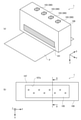
- FIG. 1 is an external view illustrating the configuration of the light irradiation device according to the first embodiment of the present invention.
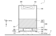
- FIG. 2 is a cross-sectional view taken along the line AA of FIG. 1 (b).
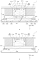
- FIG. 3 is a diagram illustrating a configuration of a light source unit provided in the light irradiation device according to the first embodiment of the present invention.
- FIG. 4 is a schematic diagram illustrating the configuration of the light irradiation device according to the first embodiment of the present invention.
- FIG. 5 is a simulation result for explaining the operation and effect of the light irradiation device according to the first embodiment of the present invention.
- FIG. 6 is a schematic diagram illustrating the configuration of the light irradiation device according to the first embodiment of the present invention.
- FIGS. 1 and 2 are views showing the configuration of the light irradiation device 1 according to the first embodiment of the present invention
- FIG. 1 (a) is a perspective view
- FIG. 1 (b) is a front view. ..
- FIG. 2 is a cross-sectional view taken along the line AA of FIG. 1 (b).
- the light irradiation device 1 of the present embodiment is a light source device incorporated in a printing device or the like to cure an ultraviolet curable ink or an ultraviolet curable resin, and is conveyed in one direction.
- FIG. 1A shows only the light irradiation device 1 for convenience of explanation, but in an actual printing device or the like, a plurality of recording heads that each apply ink of different colors irradiate the light irradiation device 1.
- the light irradiation device 1 is arranged in a narrow space on the downstream side of each recording head so as to be arranged in the transport direction of the object P.
- the transport direction of the irradiation target P is the X-axis direction (first direction)
- the arrangement direction of the LED (Light Emitting Diode) element 217 described later is the Y-axis direction (second direction)
- the LED element is the direction in which the 217 emits ultraviolet light.
- the direction in which the 217 emits ultraviolet light is defined as the Z-axis direction (third direction) and will be described.
- the ultraviolet light means light having a wavelength of 400 nm or less, but in the present specification, the ultraviolet light cures the ultraviolet curable ink applied on the irradiation target P. It is intended to mean light having a possible wavelength (eg, wavelength 250-420 nm).
- the light irradiation device 1 of the present embodiment includes a light source unit 200, a cooling fan 300, a housing 100 for accommodating the light source unit 200 and the cooling fan 300, and the like.
- the housing 100 is a box-shaped case that is long in the Y-axis direction, and is provided with a glass cover glass 105 that emits ultraviolet light on the front surface (the surface on the plus side in the Z-axis direction). Further, a pair of mirror units 108 and 109 are arranged between the light source unit 200 and the cover glass 105 so as to be separated from each other in the X-axis direction (FIG. 2), and the front surface of the cover glass 105 has an edge portion of the cover glass 105.
- a support plate 107 (support portion) for supporting the glass from the plus side in the Z-axis direction is arranged (FIGS. 1 (b) and 2).
- the support plate 107 has a rectangular opening 107a (opening) in the central portion, so that ultraviolet light that has passed through the cover glass 105 is irradiated onto the irradiation target P through the opening 107a. It has become.
- the cover glass 105 and the support plate 107 are arranged so as to cover the front surface of the housing 100, and the cover glass 105 and the support plate 107 form a part of the housing 100. There is.
- an exhaust port 101 for exhausting air in the housing 100 is formed on the left side surface (the surface on the minus side in the X-axis direction) of the housing 100, and is formed on the back surface (the surface on the minus side in the Z-axis direction) of the housing 100.
- four intake ports 103 for supplying air are formed, and a cooling fan 300 is arranged corresponding to each intake port 103 (FIGS. 1A and 2).
- the light irradiation device 1 is electrically connected to a power supply device (not shown), and power from the power supply device is supplied to an internal light source unit 200, a cooling fan 300, and the like.
- FIG. 3A and 3B are views for explaining the configuration of the light source unit 200 of the present embodiment
- FIG. 3A is a front view (a view seen from the plus side in the Z-axis direction)
- FIG. 3B is a view. It is a side view (the view seen from the minus side in the X-axis direction).
- the light source unit 200 includes four LED modules 210 arranged side by side in the Y-axis direction and a heat sink 220, and the ultraviolet light emitted from the LED module 210 is a pair of mirror units.
- the light is guided by 108 and 109, and is irradiated onto the irradiation target P through the cover glass 105 and the opening 107a on the front surface of the housing 100 (see the broken line arrow in FIG. 2).
- the LED module 210 includes a rectangular plate-shaped substrate 215 defined in the X-axis direction and the Y-axis direction, and a plurality of LED elements 217 having the same characteristics, and has an end surface (Z-axis direction) of the base plate 222 of the heat sink 220. It is fixed on the end face on the plus side).
- the substrate 215 of each LED module 210 is a rectangular wiring board made of a material having high thermal conductivity (for example, aluminum nitride), and as shown in FIG. 3A, there are five rows (for example) on the surface thereof.
- COB (Chip On Board) LED elements 217 of (X-axis direction) x 20 (Y-axis direction) are mounted. Further, in the present embodiment, the LED element 217 is located in the LED mounting area S (the area surrounded by the broken line in FIG. 3A) at the substantially central portion in the X-axis direction of the substrate 215 in the X-axis direction and the Y-axis direction. They are arranged at regular intervals (for example, 2 mm). As shown in FIG. 3B, in the present specification, for convenience of explanation, the LED elements 217 arranged in each row are sequentially arranged along the X-axis direction as LED elements 217a, 217b, and 217c. It is called 217d and 217e.
- An anode pattern (not shown) and a cathode pattern (not shown) for supplying electric power to each LED element 217 are formed on the substrate 215, and each LED element 217 is soldered to the anode pattern and the cathode pattern, respectively. Attached and electrically connected. Further, the substrate 215 is electrically connected to a driver circuit (not shown) by a wiring cable (not shown), and a drive current is supplied to each LED element 217 from the driver circuit via an anode pattern and a cathode pattern. It has become so.
- each LED element 217 When a drive current is supplied to each LED element 217, ultraviolet light (for example, a wavelength of 385 nm) having an amount of light corresponding to the drive current is emitted from each LED element 217, and a line parallel to the Y-axis direction is emitted from the LED module 210. Ultraviolet light is emitted.
- FIG. 3A in the present embodiment, four LED modules 210 are arranged in the Y-axis direction, and linear ultraviolet light from each LED module 210 is continuous in the Y-axis direction. It is configured as follows.
- the drive current supplied to each LED element 217 is adjusted so that each LED element 217 of the present embodiment emits ultraviolet light having a substantially uniform amount of light, and is emitted from the four LED modules 210.
- the line-shaped ultraviolet light has a substantially uniform light amount distribution in the X-axis direction and the Y-axis direction.
- the heat sink 220 is a so-called air-cooled heat sink that is arranged so as to be in close contact with the back surface of the substrate 215 of the LED module 210 and dissipates heat generated by each LED module 210.
- the heat sink 220 is made of a material having good thermal conductivity such as aluminum or copper, and has a thin plate-shaped base plate 222 extending in the Y-axis direction and a plurality of heat dissipation formed on a surface opposite to the surface on which the substrate 215 abuts. It has fins 225 and.
- Each radiating fin 225 has a thin plate-like shape parallel to the XZ plane, and is provided at a predetermined interval in the Y-axis direction.
- the plurality of heat radiation fins 225 are uniformly cooled by the cooling air generated by the cooling fan 300.
- each LED element 217 When a drive current flows through each LED element 217 and ultraviolet light is emitted from each LED element 217, the temperature rises due to the self-heating of the LED element 217, but the heat generated by each LED element 217 is the substrate 215 and the base plate. It is rapidly conducted to the heat radiating fins 225 via the 222, and is radiated from each heat radiating fin 225 into the surrounding air. Then, the air heated by the radiating fins 225 is quickly exhausted through the exhaust port 101 by the cooling air generated by the cooling fan 300. As described above, in the present embodiment, since each LED module 210 is uniformly cooled by the heat sink 220 and the cooling fan 300, the decrease in luminous efficiency caused by the temperature rise of the LED element 217 is suppressed.
- the pair of mirror units 108 and 109 are arranged between the light source unit 200 and the cover glass 105 so as to be separated from each other in the X-axis direction (FIG. 2), and the cover glass 105.
- a support plate 107 (support portion) that supports the edge portion of the cover glass 105 from the plus side in the Z-axis direction is arranged on the front surface (FIGS. 1 (b) and 2).
- the pair of mirror units 108 and 109 are metal plate-shaped members extending in the Y-axis direction so as to sandwich the optical path of each ultraviolet light emitted from the LED element 217 from the X-axis direction.
- the mirror units 108 and 109 extend in the Z-axis direction so as to stand substantially vertically from the cover glass 105 when viewed from the Y-axis direction, and are symmetrical with respect to the optical path of each ultraviolet light emitted from the LED element 217. Is located in.
- the mirror units 108 and 109 are provided with first reflecting surfaces 108a and 109a facing each other so as to sandwich an optical path of each ultraviolet light emitted from the LED element 217.
- the ultraviolet light emitted from the LED element 217 is generally radiated at a predetermined spread angle, and the intensity of the ultraviolet light having a larger angle component becomes weaker.
- the ultraviolet light is emitted from the LED element 217. Since the first reflecting surfaces 108a and 109a are arranged so as to sandwich the optical path of each emitted ultraviolet light, the light is guided by the first reflecting surfaces 108a and 109a including the ultraviolet light having a weak intensity and a large angle component. , Is emitted through the cover glass 105.
- the first reflecting surfaces 108a and 109a have a predetermined reflectance (for example, 90%), ultraviolet light is emitted.
- a predetermined reflectance for example, 90%
- the amount of light decreases, and as a result, the amount of light on the irradiated object P decreases. Therefore, in the present embodiment, among the ultraviolet light rays emitted from the LED element 217, the light rays having a small angle component (in order to solve such a problem and efficiently extract the ultraviolet light emitted from the LED element 217 ().
- a light ray having a spread angle ⁇ 60 ° is reflected once on the first reflecting surfaces 108a and 109a, or is emitted without being reflected, and has a large angular component (for example, a light ray having a spread angle> 60 °). Is configured to be reflected by the first reflecting surfaces 108a and 109a one or more times and then emitted (details will be described later).
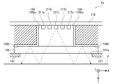
- FIG. 4 is a schematic diagram illustrating the relationship between the arrangement of the LED module 210, the mirror units 108 and 109, the cover glass 105, and the support plate 107 and the light rays emitted from each LED element 217.
- FIG. 4A is a diagram showing the relationship with ultraviolet light having a small spread angle (for example, spread angle ⁇ 60 °)
- FIG. 4B is a diagram showing a relationship with a light beam having a large spread angle (for example, spread angle>. 60 °) It is a figure which shows the relationship with the ray of ultraviolet light.
- a small spread angle for example, spread angle ⁇ 60 °
- L60a is a light ray having a spreading angle of 60 ° emitted from the LED element 217a
- L60c is a light ray having a spreading angle of 60 ° emitted from the LED element 217c
- L60e is a light beam having a spreading angle of 60 °. It is a light ray having a spread angle of 60 ° emitted from 217e
- L0a is a light ray having a spread angle of 0 ° emitted from the LED element 217a.
- L65a is a light ray having a spread angle of 65 ° emitted from the LED element 217a
- L80e is a light ray having a spread angle of 80 ° emitted from the LED element 217e.
- the ultraviolet light rays emitted from the LED elements 217b and 217d are omitted for convenience of explanation, but in reality, the LED elements 217b and 217d are also LED elements. Light rays similar to those of 217a, 217c, and 217e are emitted. Further, in FIGS.
- each LED element 217 is shown in a rectangular shape for convenience of explanation, but in reality, each LED element 217 is sufficiently thin in the Z-axis direction, and each LED element 217 is formed in a rectangular shape.
- the light emitting point of the LED element 217 is substantially located on the surface of the substrate 215.
- the width of the LED mounting area S in the X-axis direction (that is, the most upstream side in the X-axis direction (minus side in the X-axis direction)).
- the distance from the LED element 217a in the first row located in) to the LED element 217e in the fifth row located on the most downstream side in the X-axis direction (plus side in the X-axis direction) is a, and the first reflecting surface 108a.
- 109a is b
- the height of the first reflecting surfaces 108a and 109a in the Z-axis direction is h
- the distance from the substrate 215 to the support plate 107 is d
- the distance between the support plates 107 in the X-axis direction (that is, , The width of the opening 107a in the X-axis direction) is set to w, and is configured to satisfy the following equations (1) and (2).
- the light rays L60a having a spreading angle of 60 ° are reflected once by the first reflecting surface 108a and emitted through the cover glass 105, and are also emitted.
- the light is emitted through the cover glass 105 without being incident on the first reflecting surface 109a (that is, passing through the tip of the first reflecting surface 109a) (FIG. 4A).
- the light rays L60c having a spreading angle of 60 ° are reflected once by the first reflecting surfaces 108a and 109a and are emitted through the cover glass 105. ing.
- the light rays L60e having a spreading angle of 60 ° are reflected once by the first reflecting surface 109a, are emitted through the cover glass 105, and are first reflected. It is designed to be emitted through the cover glass 105 without incident on the surface 108a (that is, through the tip of the first reflecting surface 108a). Therefore, among the ultraviolet light rays emitted from each LED element 217, the light rays having a spread angle of less than 60 ° are similarly reflected once by the first reflecting surfaces 108a and 109a, or are not reflected. Is emitted through the cover glass 105.
- the light rays (light rays L60a, L60c, L60e, L0a) having a spreading angle of 60 ° or less pass through the opening 107a after passing through the cover glass 105 (that is, without being eclipsed by the support plate 107) on the irradiation target P. To reach.
- the light rays having a spread angle of more than 60 ° are the first reflecting surface. It is reflected by 108a and 109a at least once and emitted through the cover glass 105 (FIG. 4 (b)). A part of the light rays having a spreading angle of more than 60 ° (for example, the light rays L65a) pass through the opening 107a after passing through the cover glass 105 (that is, without being eclipsed by the support plate 107).
- the distance in the X-axis direction from the central axis (light emitting point) of the LED element 217a to the first reflecting surface 109a is determined. It can be expressed as ⁇ 3h from the relationship with the light ray L60a, and the distance in the X-axis direction from the central axis (light emitting point) of the LED element 217e to the first reflection surface 108a is expressed as ⁇ 3h from the relationship with the light ray L60e. Therefore, the distance b between the first reflecting surfaces 108a and 109a is set.
- the distance in the X-axis direction from the central axis (light emitting point) of the LED element 217a to one end (the end on the plus side in the X-axis direction) of the support plate 107 can be expressed as ⁇ 3d in relation to the light beam L60a.
- the distance in the X-axis direction from the central axis (light emitting point) of the LED element 217e to the other end (end on the minus side in the X-axis direction) of the support plate 107 is ⁇ 3d in relation to the light beam L60e. Since it can be represented, the distance w in the X-axis direction of the support plate 107 is w ⁇ ⁇ 3d + ⁇ 3d-a Can be expressed as, and the above equation (2) can be obtained by modifying this.
- a light ray (ultraviolet light) having a strong intensity and a spread angle of 60 ° or less is reflected once on the first reflecting surfaces 108a and 109a, or is not reflected and is irradiated. Since it reaches the object P, the influence of reflection by the first reflecting surfaces 108a and 109a (that is, a decrease in the amount of light) is suppressed.
- a light ray having a spread angle of more than 60 ° (ultraviolet light) is reflected by the first reflecting surfaces 108a and 109a at least once, but a light ray having a spread angle larger than 60 ° (ultraviolet light) is reflected at least once. Since the intensity is weak, the effect on the total amount of light emitted onto the object P to be irradiated is slight (that is, the effect of the decrease in the amount of light is small).
- FIG. 5 is a simulation result for explaining the operation and effect of the light irradiation device 1 of the present embodiment
- the horizontal axis is the distance between the support plates 107 in the X-axis direction (that is, the width of the opening 107a in the X-axis direction) w (mm). ).
- the vertical axis is the integrated light amount of the ultraviolet light emitted from the light irradiation device 1, and is a relative value with the integrated light amount when w is 100 (mm) as 1.
- the width of the LED mounting area S in the X-axis direction (that is, the most downstream side in the X-axis direction from the LED element 217a in the first row located on the upstream side in the X-axis direction (minus side in the X-axis direction) (that is, the negative side in the X-axis direction).
- the distance) a to the LED element 217e in the fifth row located on the plus side in the X-axis direction) is 10 (mm)
- the distance b between the first reflecting surfaces 108a and 109a is 15 (mm)
- the first reflecting surface is 10 (mm)
- the height h of 108a and 109a in the Z-axis direction was 5 (mm)
- the distance d from the substrate 215 to the support plate 107 was 8 (mm)
- w (mm) was changed to obtain the integrated light amount.
- the integrated light amount is about 0.9
- the integrated light amount does not decrease (that is, the ultraviolet light emitted from the light irradiation device 1). Reaches on the irradiated object P without being eclipsed by the support plate 107).
- the conditions of the above equations (1) and (2) and the above simulation result are substantially the same, and when the above equations (1) and (2) are satisfied, the integrated amount of ultraviolet light emitted from the light irradiation device 1 is achieved. It can be seen that there is almost no decrease (that is, the integrated light amount is 0.9 or more).
- the LED elements 217 are arranged in a manner of 5 rows (X-axis direction) ⁇ 20 (Y-axis direction), but the configuration is limited to such a configuration.
- the LED elements 217 may be arranged in n (n is an integer of 2 or more) along the Y-axis direction and in m columns (m is an integer of 2 or more) along the X-axis direction.
- first reflecting surfaces 108a and 109a of the present embodiment extend in the Z-axis direction so as to stand up substantially vertically from the cover glass 105, and are arranged symmetrically with respect to the optical path of each ultraviolet light emitted from the LED element 217.
- first reflecting surfaces 108a and 109a do not necessarily have to be parallel to the Z-axis direction.
- the first reflecting surfaces 108a and 109a spread in a C shape with respect to the Z-axis direction. It can also be arranged as follows.
- the positional relationship between the LED element 217, the first reflecting surfaces 108a and 109a, and the support plate 107 has been described as satisfying the equations (1) and (2), but the configuration is not necessarily limited to such a configuration.
- it can be configured to satisfy the following equations (3) and (4).
- FIG. 6 is a diagram illustrating a configuration of a light irradiation device 1A according to a second embodiment of the present invention.
- the XZ cross section of the pair of mirror units 108 and 109 is L-shaped, and the tip portion of the first reflection surface 108a of the mirror unit 108 is formed.
- the second reflective mirror 108b extending in the negative side in the X-axis direction so as to face the cover glass 105, and the positive side in the X-axis direction so as to face the cover glass 105 from the tip of the first reflective surface 109a of the mirror unit 109. It differs from the light irradiation device 1 of the first embodiment in that it includes a third reflection mirror 109b that extends.
- the second reflection mirror 108b and the third reflection mirror 109b emit ultraviolet light emitted from the LED element 217 (LED element 217c in FIG. 6) and are reflected by the irradiation object P to be irradiated. It is configured to reflect again toward P (see the dashed arrow in FIG. 6). Therefore, according to the configuration of the present embodiment, the ultraviolet light that did not contribute to the curing of the ultraviolet curable ink on the irradiation target P (that is, the ultraviolet light reflected by the irradiation target P) is again the irradiation target P. It becomes possible to further improve the utilization efficiency of ultraviolet light.
- the width of the second reflection mirror 108b and the third reflection mirror 109b in the X-axis direction is preferably as wide as possible so that the reflection can be performed a plurality of times.
- the width of the cover glass 105 in the X-axis direction is wide.
- the distance between the support plates 107 in the X-axis direction (that is, the width of the opening 107a in the X-axis direction) may be widened.
- both the second reflection mirror 108b and the third reflection mirror 109b may be provided.
- the mirror units 108 and 109 of the present embodiment have an L-shaped XZ cross section, and the first reflecting surface 108a and the second reflecting mirror 108b are integrally formed with the first reflecting surface 109a.
- the third reflection mirror 109b is integrally formed, the present invention is not necessarily limited to such a configuration.
- the first reflecting surface 108a and the second reflecting mirror 108b, and the first reflecting surface 109a and the third reflecting mirror 109b may be formed separately from each other.
- Light irradiation device 1A Light irradiation device 100: Housing 101: Exhaust port 103: Intake port 105: Cover glass 107: Support plate 107a: Opening 108: Mirror unit 108a: First reflection surface 108b: Second reflection mirror 109 : Mirror unit 109a: First reflective surface 109b: Third reflective mirror 200: Light source unit 210: LED module 215: Board 217: LED element 220: Heat sink 222: Base plate 225: Heat dissipation fin 300: Cooling fan
Abstract
A light irradiation device for irradiating, with light, an irradiation object that is capable of moving relative thereto, the light irradiation device comprising: a substrate; a plurality of light-emitting elements which are arranged on the substrate in an array of n-units (n is an integer of 2 or more) by m-rows (m is an integer of 2 or more); a cover glass which allows light from the respective light-emitting elements to pass therethrough; a support part which has an opening for light to pass therethrough and which supports the cover glass; and a pair of first reflective mirrors which are disposed between the substrate and the cover glass and which is for guiding light, wherein the formulae (1) and (2) are satisfied, where a represents the distance from a light-emitting element in the first row positioned on the most upstream side to a light-emitting element in the m-th row positioned on the most downstream side, b represents the interval between the pair of first reflective mirrors, h represents the height of the pair of first reflective mirrors, d represents the distance from the substrate to the support part, and w represents the width of the opening in a first direction. (1): h≤(a+b)/2√3, (2): w≥d•2√3-a
Description
本発明は、一方向に搬送される照射対象物に対して光を照射する光照射装置に関する。
The present invention relates to a light irradiation device that irradiates light on an irradiation target object conveyed in one direction.
従来、紫外光の照射によって硬化するUVインクを用いて印刷を行なう印刷装置が知られている。このような印刷装置では、ヘッドのノズルから媒体にインクを吐出した後、媒体に形成されたドットに紫外光を照射する。紫外光の照射により、ドットが硬化して媒体に定着するので、液体を吸収しにくい媒体に対しても良好な印刷を行うことができる。
Conventionally, a printing device that prints using UV ink that is cured by irradiation with ultraviolet light is known. In such a printing apparatus, after ink is ejected from the nozzle of the head to the medium, the dots formed on the medium are irradiated with ultraviolet light. By irradiating with ultraviolet light, the dots are cured and fixed on the medium, so that good printing can be performed even on a medium that does not easily absorb liquid.
このような印刷装置に用いられる紫外光照射装置においては、近年、消費電力の削減、長寿命化、装置サイズのコンパクト化の要請から、従来の放電ランプに替えて、LED(Light Emitting Diode)素子を光源として利用したものが実用に供されている(例えば、特許文献1)。
In recent years, in the ultraviolet light irradiation device used for such printing devices, LED (Light Emitting Diode) elements have been replaced with conventional discharge lamps in order to reduce power consumption, extend the service life, and reduce the size of the device. Is put into practical use as a light source (for example, Patent Document 1).
特許文献1に記載の紫外光照射装置は、照射対象物の搬送方向と直交する方向に沿って並ぶ複数の紫外光光源(紫外線LED)を有する光源ユニットと、光源ユニットと照射対象物との間に配置され、光源ユニットを、搬送方向の上流側及び下流側から挟むように配置された一対の反射部材と、を備え、紫外光光源からの紫外光を一対の反射板で導光して出射することで紫外光に指向性を持たせる構成を採っている。
The ultraviolet light irradiation device described in Patent Document 1 is between a light source unit having a plurality of ultraviolet light sources (ultraviolet LEDs) arranged along a direction orthogonal to the transport direction of the object to be irradiated, and between the light source unit and the object to be irradiated. The light source unit is provided with a pair of reflecting members arranged so as to sandwich the light source unit from the upstream side and the downstream side in the transport direction, and the ultraviolet light from the ultraviolet light source is guided and emitted by the pair of reflecting plates. By doing so, we have adopted a structure that gives directional light to ultraviolet light.
しかしながら、特許文献1のような構成を採ると、反射部材が所定の反射率を有するために、紫外光が反射部材によって反射されるたびに紫外光の光量(強度)が低下してしまい、照射対象物上において所定の光量(つまり、UVインクを確実に硬化させるための光量)を得ようとすると、光量の低下分を補うために、紫外光LEDの数を増やす必要が生じる。そして、その結果、装置のコストアップ、サイズアップ、消費電力のアップを招いてしまうといった問題が発生する。そのため、LEDの数を増やすことなく、効率のよい照射が可能な光照射装置が求められている。
However, when the configuration as in Patent Document 1 is adopted, since the reflective member has a predetermined reflectance, the amount (intensity) of the ultraviolet light decreases each time the ultraviolet light is reflected by the reflective member, and the irradiation is performed. In order to obtain a predetermined amount of light (that is, the amount of light for reliably curing the UV ink) on the object, it is necessary to increase the number of ultraviolet light LEDs in order to compensate for the decrease in the amount of light. As a result, there arises a problem that the cost of the device is increased, the size is increased, and the power consumption is increased. Therefore, there is a demand for a light irradiation device capable of efficient irradiation without increasing the number of LEDs.
本発明は、上記の事情に鑑みてなされたものであり、出射光に指向性を持たせつつも、効率のよい照射が可能な光照射装置を提供することを目的とする。
The present invention has been made in view of the above circumstances, and an object of the present invention is to provide a light irradiation device capable of efficient irradiation while giving directivity to emitted light.
上記目的を達成するため、本発明の光照射装置は、第1方向に沿って相対的に移動可能な照射対象物に対して光を照射する光照射装置であって、第1方向と第1方向と直交する第2方向によって規定される基板と、基板上に第2方向に沿ってn個(nは2以上の整数)、第1方向に沿ってm列(mは2以上の整数)に並べられ、第1方向及び第2方向と直交する第3方向に光軸の向きを揃えて配置された複数の発光素子と、複数の発光素子から出射された光が透過するカバーガラスと、カバーガラスを透過した光が通る開口部を有し、カバーガラスを支持する支持部と、複数の発光素子の光路を第1方向に挟むように、基板とカバーガラスとの間に配置され、光を導光する一対の第1反射ミラーと、を備え、第2方向から見たときに、最も第1方向上流側に位置する第1列目の発光素子から最も第1方向下流側に位置する第m列目の発光素子までの距離をaとし、一対の第1反射ミラーの間隔をbとし、一対の第1反射ミラーの第3方向の高さをhとし、基板から支持部までの距離をdとし、開口部の第1方向の幅をwとしたときに、下式(1)及び(2)を満たすことを特徴とする。
h≦(a+b)/2√3 ・・・(1)
w≧d・2√3-a ・・・(2)
In order to achieve the above object, the light irradiation device of the present invention is a light irradiation device that irradiates light to an irradiation object that can move relatively along a first direction, and is a first direction and a first light irradiation device. A substrate defined by a second direction orthogonal to the direction, n on the substrate along the second direction (n is an integer of 2 or more), and m columns along the first direction (m is an integer of 2 or more). A plurality of light emitting elements arranged in the same direction in the third direction orthogonal to the first direction and the second direction, and a cover glass through which light emitted from the plurality of light emitting elements is transmitted. It has an opening through which light transmitted through the cover glass passes, and is arranged between the substrate and the cover glass so as to sandwich the light path of the plurality of light emitting elements in the first direction and the support portion that supports the cover glass. It is provided with a pair of first reflection mirrors for guiding light, and is located on the downstream side in the first direction from the light emitting element in the first row located on the upstream side in the first direction when viewed from the second direction. The distance to the light emitting element in the mth row is a, the distance between the pair of first reflection mirrors is b, the height of the pair of first reflection mirrors in the third direction is h, and the distance from the substrate to the support portion. Is d, and when the width of the opening in the first direction is w, the following equations (1) and (2) are satisfied.
h ≦ (a + b) / 2√3 ・ ・ ・ (1)
w ≧ d ・ 2√3-a ・ ・ ・ (2)
このような構成によれば、強度の強い、拡がり角が60°以下の光線(紫外光)が第1反射面108a、109aに1回反射されるか、又は反射されずに、照射対象物P上に到達するため、第1反射面108a、109aによる反射の影響(つまり、光量の減少)は殆ど発生しない。従って、第1反射面108a、109aによって出射光に指向性を持たせつつも、効率のよい照射が可能となる。
According to such a configuration, a light ray (ultraviolet light) having a strong spreading angle of 60 ° or less is reflected once on the first reflecting surfaces 108a and 109a, or is not reflected and is not reflected, and the irradiated object P. Since it reaches the top, the influence of reflection by the first reflecting surfaces 108a and 109a (that is, a decrease in the amount of light) hardly occurs. Therefore, the first reflecting surfaces 108a and 109a enable efficient irradiation while giving directivity to the emitted light.
また、第1方向上流側に位置する第1反射ミラーの先端部からカバーガラスと対向するように第1方向上流側に延び、照射対象物によって反射された光を照射対象物に向かって反射する第2反射ミラーを備えることができる。また、この場合、第2反射ミラーが第1方向上流側に位置する第1反射ミラーと一体的に形成されていることが望ましい。
Further, it extends from the tip of the first reflection mirror located on the upstream side in the first direction to the upstream side in the first direction so as to face the cover glass, and reflects the light reflected by the irradiation target toward the irradiation target. A second reflection mirror can be provided. Further, in this case, it is desirable that the second reflection mirror is integrally formed with the first reflection mirror located on the upstream side in the first direction.
また、第1方向下流側に位置する第1反射ミラーの先端部からカバーガラスと対向するように第1方向下流側に延び、照射対象物によって反射された光を照射対象物に向かって反射する第3反射ミラーを備えることができる。また、この場合、第3反射ミラーが第1方向下流側に位置する第1反射ミラーと一体的に形成されていることが望ましい。
Further, it extends from the tip of the first reflection mirror located on the downstream side in the first direction to the downstream side in the first direction so as to face the cover glass, and reflects the light reflected by the irradiation target toward the irradiation target. A third reflection mirror can be provided. Further, in this case, it is desirable that the third reflection mirror is integrally formed with the first reflection mirror located on the downstream side in the first direction.
また、基板、複数の発光素子、及び一対の第1反射ミラーを収容する筐体を有し、支持部及びカバーガラスが、筐体の一部を構成していることが望ましい。
Further, it is desirable that the housing has a substrate, a plurality of light emitting elements, and a pair of first reflection mirrors, and the support portion and the cover glass form a part of the housing.
また、光は、紫外線波長域の光であることが望ましい。また、この場合、照射対象物は、シート状の形状を呈し、紫外線波長域の光が照射対象物の表面上に塗布されたインキを硬化させるように構成することができる。
Further, it is desirable that the light is light in the ultraviolet wavelength range. Further, in this case, the irradiation target has a sheet-like shape, and the light in the ultraviolet wavelength range can be configured to cure the ink applied on the surface of the irradiation target.
以上のように、本発明によれば、出射光に指向性を持たせつつも、効率のよい照射が可能な光照射装置が実現される。
As described above, according to the present invention, a light irradiation device capable of efficient irradiation while giving directivity to the emitted light is realized.
以下、本発明の実施形態について図面を参照して詳細に説明する。なお、図中同一又は相当部分には同一の符号を付してその説明は繰り返さない。
Hereinafter, embodiments of the present invention will be described in detail with reference to the drawings. The same or corresponding parts in the drawings are designated by the same reference numerals and the description thereof will not be repeated.
(第1の実施形態)
図1及び図2は、本発明の第1の実施形態に係る光照射装置1の構成を示す図であり、図1(a)は斜視図であり、図1(b)は正面図である。また、図2は、図1(b)のA-A線断面図である。図1及び図2に示すように、本実施形態の光照射装置1は、印刷装置等に組み込まれて、紫外線硬化型インキや紫外線硬化樹脂を硬化させる光源装置であり、一方向に搬送される照射対象物P(例えば、シート状の記録媒体等)の上方に配置され、照射対象物Pに対してライン状の紫外光を出射する。なお、図1(a)においては、説明の便宜のため、光照射装置1のみを示しているが、実際の印刷装置等においては、異なる色のインクをそれぞれ付与する、複数の記録ヘッドが照射対象物Pの搬送方向に並び、各記録ヘッドの下流側の狭い空間に光照射装置1が配置される。また、本明細書においては、照射対象物Pの搬送方向をX軸方向(第1方向)、後述するLED(Light Emitting Diode)素子217の配列方向をY軸方向(第2方向)、LED素子217が紫外光を出射する方向をZ軸方向(第3方向)と定義して説明する。また、一般に、紫外光とは、波長400nm以下の光を意味するものとされているが、本明細書において、紫外光とは、照射対象物P上に塗布された紫外線硬化型インキを硬化させることが可能な波長(例えば、波長250~420nm)の光を意味するものとする。 (First Embodiment)
1 and 2 are views showing the configuration of thelight irradiation device 1 according to the first embodiment of the present invention, FIG. 1 (a) is a perspective view, and FIG. 1 (b) is a front view. .. Further, FIG. 2 is a cross-sectional view taken along the line AA of FIG. 1 (b). As shown in FIGS. 1 and 2, the light irradiation device 1 of the present embodiment is a light source device incorporated in a printing device or the like to cure an ultraviolet curable ink or an ultraviolet curable resin, and is conveyed in one direction. It is arranged above the irradiation target object P (for example, a sheet-shaped recording medium or the like), and emits line-shaped ultraviolet light to the irradiation target object P. Note that FIG. 1A shows only the light irradiation device 1 for convenience of explanation, but in an actual printing device or the like, a plurality of recording heads that each apply ink of different colors irradiate the light irradiation device 1. The light irradiation device 1 is arranged in a narrow space on the downstream side of each recording head so as to be arranged in the transport direction of the object P. Further, in the present specification, the transport direction of the irradiation target P is the X-axis direction (first direction), the arrangement direction of the LED (Light Emitting Diode) element 217 described later is the Y-axis direction (second direction), and the LED element. The direction in which the 217 emits ultraviolet light is defined as the Z-axis direction (third direction) and will be described. Further, in general, the ultraviolet light means light having a wavelength of 400 nm or less, but in the present specification, the ultraviolet light cures the ultraviolet curable ink applied on the irradiation target P. It is intended to mean light having a possible wavelength (eg, wavelength 250-420 nm).
図1及び図2は、本発明の第1の実施形態に係る光照射装置1の構成を示す図であり、図1(a)は斜視図であり、図1(b)は正面図である。また、図2は、図1(b)のA-A線断面図である。図1及び図2に示すように、本実施形態の光照射装置1は、印刷装置等に組み込まれて、紫外線硬化型インキや紫外線硬化樹脂を硬化させる光源装置であり、一方向に搬送される照射対象物P(例えば、シート状の記録媒体等)の上方に配置され、照射対象物Pに対してライン状の紫外光を出射する。なお、図1(a)においては、説明の便宜のため、光照射装置1のみを示しているが、実際の印刷装置等においては、異なる色のインクをそれぞれ付与する、複数の記録ヘッドが照射対象物Pの搬送方向に並び、各記録ヘッドの下流側の狭い空間に光照射装置1が配置される。また、本明細書においては、照射対象物Pの搬送方向をX軸方向(第1方向)、後述するLED(Light Emitting Diode)素子217の配列方向をY軸方向(第2方向)、LED素子217が紫外光を出射する方向をZ軸方向(第3方向)と定義して説明する。また、一般に、紫外光とは、波長400nm以下の光を意味するものとされているが、本明細書において、紫外光とは、照射対象物P上に塗布された紫外線硬化型インキを硬化させることが可能な波長(例えば、波長250~420nm)の光を意味するものとする。 (First Embodiment)
1 and 2 are views showing the configuration of the
図1及び図2に示すように、本実施形態の光照射装置1は、光源ユニット200と、冷却ファン300と、光源ユニット200及び冷却ファン300を収容する筐体100等を備えている。
As shown in FIGS. 1 and 2, the light irradiation device 1 of the present embodiment includes a light source unit 200, a cooling fan 300, a housing 100 for accommodating the light source unit 200 and the cooling fan 300, and the like.
筐体100は、Y軸方向に長い箱形のケースであり、前面(Z軸方向プラス側の面)に紫外光が出射されるガラス製のカバーガラス105を備えている。また、光源ユニット200とカバーガラス105の間には、一対のミラーユニット108、109がX軸方向に離間して配置され(図2)、カバーガラス105の前面には、カバーガラス105の縁部をZ軸方向プラス側から支持する支持プレート107(支持部)が配置されている(図1(b)、図2)。支持プレート107は、中央部に矩形状の開口107a(開口部)を有しており、カバーガラス105を通過した紫外光は、開口107aを通って、照射対象物P上に照射されるようになっている。このように、本実施形態においては、カバーガラス105と支持プレート107が筐体100の正面を覆うように配置されており、カバーガラス105と支持プレート107が筐体100の一部を構成している。
The housing 100 is a box-shaped case that is long in the Y-axis direction, and is provided with a glass cover glass 105 that emits ultraviolet light on the front surface (the surface on the plus side in the Z-axis direction). Further, a pair of mirror units 108 and 109 are arranged between the light source unit 200 and the cover glass 105 so as to be separated from each other in the X-axis direction (FIG. 2), and the front surface of the cover glass 105 has an edge portion of the cover glass 105. A support plate 107 (support portion) for supporting the glass from the plus side in the Z-axis direction is arranged (FIGS. 1 (b) and 2). The support plate 107 has a rectangular opening 107a (opening) in the central portion, so that ultraviolet light that has passed through the cover glass 105 is irradiated onto the irradiation target P through the opening 107a. It has become. As described above, in the present embodiment, the cover glass 105 and the support plate 107 are arranged so as to cover the front surface of the housing 100, and the cover glass 105 and the support plate 107 form a part of the housing 100. There is.
また、筐体100の左側面(X軸方向マイナス側の面)には筐体100内の空気を排気する排気口101が形成され、筐体100の背面(Z軸方向マイナス側の面)には、筐体100内に空気を供給する4個の吸気口103が形成され、各吸気口103に対応して冷却ファン300が配置されている(図1(a)、図2)。光照射装置1は、不図示の電源装置と電気的に接続され、電源装置からの電力が内部の光源ユニット200、冷却ファン300等に供給されるようになっている。
Further, an exhaust port 101 for exhausting air in the housing 100 is formed on the left side surface (the surface on the minus side in the X-axis direction) of the housing 100, and is formed on the back surface (the surface on the minus side in the Z-axis direction) of the housing 100. In the housing 100, four intake ports 103 for supplying air are formed, and a cooling fan 300 is arranged corresponding to each intake port 103 (FIGS. 1A and 2). The light irradiation device 1 is electrically connected to a power supply device (not shown), and power from the power supply device is supplied to an internal light source unit 200, a cooling fan 300, and the like.
図3は、本実施形態の光源ユニット200の構成を説明する図であり、図3(a)は、正面図(Z軸方向プラス側から見た図)であり、図3(b)は、側面図(X軸方向マイナス側から見た図)である。図3に示すように、光源ユニット200は、Y軸方向に並べて配置された4個のLEDモジュール210と、ヒートシンク220を備えており、LEDモジュール210から出射される紫外光は、一対のミラーユニット108、109によって導光され、筐体100の前面のカバーガラス105、開口107aを通って照射対象物P上に照射されるようになっている(図2の破線矢印参照)。
3A and 3B are views for explaining the configuration of the light source unit 200 of the present embodiment, FIG. 3A is a front view (a view seen from the plus side in the Z-axis direction), and FIG. 3B is a view. It is a side view (the view seen from the minus side in the X-axis direction). As shown in FIG. 3, the light source unit 200 includes four LED modules 210 arranged side by side in the Y-axis direction and a heat sink 220, and the ultraviolet light emitted from the LED module 210 is a pair of mirror units. The light is guided by 108 and 109, and is irradiated onto the irradiation target P through the cover glass 105 and the opening 107a on the front surface of the housing 100 (see the broken line arrow in FIG. 2).
LEDモジュール210は、X軸方向及びY軸方向で規定される矩形板状の基板215と、同じ特性を有する複数のLED素子217とを備えており、ヒートシンク220のベースプレート222の端面(Z軸方向プラス側の端面)上に固定されている。
The LED module 210 includes a rectangular plate-shaped substrate 215 defined in the X-axis direction and the Y-axis direction, and a plurality of LED elements 217 having the same characteristics, and has an end surface (Z-axis direction) of the base plate 222 of the heat sink 220. It is fixed on the end face on the plus side).
各LEDモジュール210の基板215は、熱伝導率の高い材料(例えば、窒化アルミニウム)で形成された矩形状配線基板であり、図3(a)に示すように、その表面には、5列(X軸方向)×20個(Y軸方向)のLED素子217が、COB(Chip On Board)実装されている。また、本実施形態においては、LED素子217は、基板215のX軸方向略中央部のLED搭載領域S(図3(a)において破線で囲む領域)内において、X軸方向及びY軸方向に一定の間隔(例えば、2mm)をおいて配置されている。なお、図3(b)に示すように、本明細書においては、説明の便宜のため、各列に配置されるLED素子217を、X軸方向に沿って順に、LED素子217a、217b、217c、217d、217eと称する。
The substrate 215 of each LED module 210 is a rectangular wiring board made of a material having high thermal conductivity (for example, aluminum nitride), and as shown in FIG. 3A, there are five rows (for example) on the surface thereof. COB (Chip On Board) LED elements 217 of (X-axis direction) x 20 (Y-axis direction) are mounted. Further, in the present embodiment, the LED element 217 is located in the LED mounting area S (the area surrounded by the broken line in FIG. 3A) at the substantially central portion in the X-axis direction of the substrate 215 in the X-axis direction and the Y-axis direction. They are arranged at regular intervals (for example, 2 mm). As shown in FIG. 3B, in the present specification, for convenience of explanation, the LED elements 217 arranged in each row are sequentially arranged along the X-axis direction as LED elements 217a, 217b, and 217c. It is called 217d and 217e.
基板215上には、各LED素子217に電力を供給するためのアノードパターン(不図示)及びカソードパターン(不図示)が形成されており、各LED素子217は、アノードパターン及びカソードパターンにそれぞれハンダ付けされ、電気的に接続されている。また、基板215は、不図示の配線ケーブルによって不図示のドライバ回路と電気的に接続されており、各LED素子217には、アノードパターン及びカソードパターンを介して、ドライバ回路から駆動電流が供給されるようになっている。各LED素子217に駆動電流が供給されると、各LED素子217からは駆動電流に応じた光量の紫外光(例えば、波長385nm)が出射され、LEDモジュール210からはY軸方向に平行なライン状の紫外光が出射される。図3(a)に示すように、本実施形態においては、4個のLEDモジュール210がY軸方向に並べられており、各LEDモジュール210からのライン状の紫外光がY軸方向に連続するように構成されている。なお、本実施形態の各LED素子217は、略一様な光量の紫外光を出射するように各LED素子217に供給される駆動電流が調整されており、4個のLEDモジュール210から出射されるライン状の紫外光は、X軸方向及びY軸方向において略均一な光量分布を有している。
An anode pattern (not shown) and a cathode pattern (not shown) for supplying electric power to each LED element 217 are formed on the substrate 215, and each LED element 217 is soldered to the anode pattern and the cathode pattern, respectively. Attached and electrically connected. Further, the substrate 215 is electrically connected to a driver circuit (not shown) by a wiring cable (not shown), and a drive current is supplied to each LED element 217 from the driver circuit via an anode pattern and a cathode pattern. It has become so. When a drive current is supplied to each LED element 217, ultraviolet light (for example, a wavelength of 385 nm) having an amount of light corresponding to the drive current is emitted from each LED element 217, and a line parallel to the Y-axis direction is emitted from the LED module 210. Ultraviolet light is emitted. As shown in FIG. 3A, in the present embodiment, four LED modules 210 are arranged in the Y-axis direction, and linear ultraviolet light from each LED module 210 is continuous in the Y-axis direction. It is configured as follows. The drive current supplied to each LED element 217 is adjusted so that each LED element 217 of the present embodiment emits ultraviolet light having a substantially uniform amount of light, and is emitted from the four LED modules 210. The line-shaped ultraviolet light has a substantially uniform light amount distribution in the X-axis direction and the Y-axis direction.
ヒートシンク220は、LEDモジュール210の基板215の裏面に密着するように配置され、各LEDモジュール210で発生した熱を放熱する、いわゆる空冷ヒートシンクである。ヒートシンク220は、アルミニウムや銅等の熱伝導性の良好な材料からなり、Y軸方向に延びる薄板状のベースプレート222と、基板215が当接する面とは反対側の面に形成された複数の放熱フィン225と、を備えている。各放熱フィン225は、X-Z平面に平行な薄板状の形状を呈し、Y軸方向に所定の間隔をおいて設けられている。なお、本実施形態においては、冷却ファン300によって生成される冷却風によって、複数の放熱フィン225が一様に冷却されるようになっている。
The heat sink 220 is a so-called air-cooled heat sink that is arranged so as to be in close contact with the back surface of the substrate 215 of the LED module 210 and dissipates heat generated by each LED module 210. The heat sink 220 is made of a material having good thermal conductivity such as aluminum or copper, and has a thin plate-shaped base plate 222 extending in the Y-axis direction and a plurality of heat dissipation formed on a surface opposite to the surface on which the substrate 215 abuts. It has fins 225 and. Each radiating fin 225 has a thin plate-like shape parallel to the XZ plane, and is provided at a predetermined interval in the Y-axis direction. In this embodiment, the plurality of heat radiation fins 225 are uniformly cooled by the cooling air generated by the cooling fan 300.
各LED素子217に駆動電流が流れ、各LED素子217から紫外光が出射されると、LED素子217の自己発熱により温度が上昇するが、各LED素子217で発生した熱は、基板215及びベースプレート222を介して、放熱フィン225に速やかに伝導され、各放熱フィン225から周辺の空気中に放熱される。そして、放熱フィン225によって加熱された空気は、冷却ファン300によって生成される冷却風によって排気口101を通って速やかに排気される。このように、本実施形態においては、ヒートシンク220と冷却ファン300によって各LEDモジュール210が一様に冷却されるため、LED素子217の温度上昇によって生じる発光効率の低下が抑制される。
When a drive current flows through each LED element 217 and ultraviolet light is emitted from each LED element 217, the temperature rises due to the self-heating of the LED element 217, but the heat generated by each LED element 217 is the substrate 215 and the base plate. It is rapidly conducted to the heat radiating fins 225 via the 222, and is radiated from each heat radiating fin 225 into the surrounding air. Then, the air heated by the radiating fins 225 is quickly exhausted through the exhaust port 101 by the cooling air generated by the cooling fan 300. As described above, in the present embodiment, since each LED module 210 is uniformly cooled by the heat sink 220 and the cooling fan 300, the decrease in luminous efficiency caused by the temperature rise of the LED element 217 is suppressed.
なお、上述したように、本実施形態においては、光源ユニット200とカバーガラス105の間に、一対のミラーユニット108、109がX軸方向に離間して配置され(図2)、カバーガラス105の前面には、カバーガラス105の縁部をZ軸方向プラス側から支持する支持プレート107(支持部)が配置されている(図1(b)、図2)。
As described above, in the present embodiment, the pair of mirror units 108 and 109 are arranged between the light source unit 200 and the cover glass 105 so as to be separated from each other in the X-axis direction (FIG. 2), and the cover glass 105. A support plate 107 (support portion) that supports the edge portion of the cover glass 105 from the plus side in the Z-axis direction is arranged on the front surface (FIGS. 1 (b) and 2).
図2に示すように、一対のミラーユニット108、109は、LED素子217から出射される各紫外光の光路をX軸方向から挟むようにY軸方向に延びる金属製の板状部材である。各ミラーユニット108、109は、Y軸方向から見たときに、カバーガラス105から略垂直に起立するようにZ軸方向に延び、LED素子217から出射される各紫外光の光路を挟んで対称に配置されている。また、各ミラーユニット108、109は、LED素子217から出射される各紫外光の光路を挟むように対向する第1反射面108a、109aを備えている。
As shown in FIG. 2, the pair of mirror units 108 and 109 are metal plate-shaped members extending in the Y-axis direction so as to sandwich the optical path of each ultraviolet light emitted from the LED element 217 from the X-axis direction. The mirror units 108 and 109 extend in the Z-axis direction so as to stand substantially vertically from the cover glass 105 when viewed from the Y-axis direction, and are symmetrical with respect to the optical path of each ultraviolet light emitted from the LED element 217. Is located in. Further, the mirror units 108 and 109 are provided with first reflecting surfaces 108a and 109a facing each other so as to sandwich an optical path of each ultraviolet light emitted from the LED element 217.
LED素子217から出射される紫外光は、一般に、所定の拡がり角で発散され、角度成分の大きい紫外光ほど強度が弱くなることが知られているが、本実施形態においては、LED素子217から出射される各紫外光の光路を挟むように第1反射面108a、109aが配置されているため、強度が弱く角度成分の大きい紫外光も含めて、第1反射面108a、109aによって導光され、カバーガラス105を通って出射される。
しかしながら、このような構成(つまり、第1反射面108a、109aによって導光する構成)を採ると、第1反射面108a、109aが所定の反射率(例えば、90%)を有するため、紫外光が第1反射面108a、109aによって反射されるたびに光量が減少してしまい、結果として、照射対象物P上での光量が減少してしまうといった問題が発生する。
そこで、本実施形態においては、かかる問題を解決し、LED素子217から出射される紫外光を効率よく取り出せるように、LED素子217から出射される紫外光の光線のうち、角度成分の小さい光線(例えば、拡がり角≦60°の光線)は第1反射面108a、109aに1回反射されるか、又は反射されずに出射され、角度成分の大きい光線(例えば、拡がり角>60°の光線)は第1反射面108a、109aに1回以上反射されて出射されるように構成している(詳細は後述)。 It is known that the ultraviolet light emitted from theLED element 217 is generally radiated at a predetermined spread angle, and the intensity of the ultraviolet light having a larger angle component becomes weaker. However, in the present embodiment, the ultraviolet light is emitted from the LED element 217. Since the first reflecting surfaces 108a and 109a are arranged so as to sandwich the optical path of each emitted ultraviolet light, the light is guided by the first reflecting surfaces 108a and 109a including the ultraviolet light having a weak intensity and a large angle component. , Is emitted through the cover glass 105.
However, when such a configuration (that is, a configuration in which light is guided by the first reflecting surfaces 108a and 109a) is adopted, since the first reflecting surfaces 108a and 109a have a predetermined reflectance (for example, 90%), ultraviolet light is emitted. However, each time the light is reflected by the first reflecting surfaces 108a and 109a, the amount of light decreases, and as a result, the amount of light on the irradiated object P decreases.
Therefore, in the present embodiment, among the ultraviolet light rays emitted from theLED element 217, the light rays having a small angle component (in order to solve such a problem and efficiently extract the ultraviolet light emitted from the LED element 217 (). For example, a light ray having a spread angle ≤ 60 °) is reflected once on the first reflecting surfaces 108a and 109a, or is emitted without being reflected, and has a large angular component (for example, a light ray having a spread angle> 60 °). Is configured to be reflected by the first reflecting surfaces 108a and 109a one or more times and then emitted (details will be described later).
しかしながら、このような構成(つまり、第1反射面108a、109aによって導光する構成)を採ると、第1反射面108a、109aが所定の反射率(例えば、90%)を有するため、紫外光が第1反射面108a、109aによって反射されるたびに光量が減少してしまい、結果として、照射対象物P上での光量が減少してしまうといった問題が発生する。
そこで、本実施形態においては、かかる問題を解決し、LED素子217から出射される紫外光を効率よく取り出せるように、LED素子217から出射される紫外光の光線のうち、角度成分の小さい光線(例えば、拡がり角≦60°の光線)は第1反射面108a、109aに1回反射されるか、又は反射されずに出射され、角度成分の大きい光線(例えば、拡がり角>60°の光線)は第1反射面108a、109aに1回以上反射されて出射されるように構成している(詳細は後述)。 It is known that the ultraviolet light emitted from the
However, when such a configuration (that is, a configuration in which light is guided by the first reflecting
Therefore, in the present embodiment, among the ultraviolet light rays emitted from the
以下、一対のミラーユニット108、109の第1反射面108a、109aの機能について詳述する。
図4は、LEDモジュール210、ミラーユニット108、109、カバーガラス105、支持プレート107の配置と、各LED素子217から出射される光線との関係を説明する模式図である。図4(a)は、拡がり角の小さい(例えば、拡がり角≦60°)紫外光の光線との関係を示す図であり、図4(b)は、拡がり角の大きい(例えば、拡がり角>60°)紫外光の光線との関係を示す図である。図4(a)において、L60aは、LED素子217aから出射される拡がり角60°の光線であり、L60cは、LED素子217cから出射される拡がり角60°の光線であり、L60eは、LED素子217eから出射される拡がり角60°の光線であり、L0aは、LED素子217aから出射される拡がり角0°の光線である。また、図4(b)において、L65aは、LED素子217aから出射される拡がり角65°の光線であり、L80eは、LED素子217eから出射される拡がり角80°の光線である。なお、図4(a)、図4(b)において、LED素子217b、217dから出射される紫外光の光線ついては説明の便宜上省略しているが、実際にはLED素子217b、217dからもLED素子217a、217c、217eと同様の光線が出射される。また、図4(a)、図4(b)においては、説明の便宜上、各LED素子217の形状を矩形状に示すが、実際には各LED素子217はZ軸方向に十分に薄く、各LED素子217の発光点は、実質的に基板215の表面に位置している。 Hereinafter, the functions of the first reflecting surfaces 108a and 109a of the pair of mirror units 108 and 109 will be described in detail.
FIG. 4 is a schematic diagram illustrating the relationship between the arrangement of theLED module 210, the mirror units 108 and 109, the cover glass 105, and the support plate 107 and the light rays emitted from each LED element 217. FIG. 4A is a diagram showing the relationship with ultraviolet light having a small spread angle (for example, spread angle ≤ 60 °), and FIG. 4B is a diagram showing a relationship with a light beam having a large spread angle (for example, spread angle>. 60 °) It is a figure which shows the relationship with the ray of ultraviolet light. In FIG. 4A, L60a is a light ray having a spreading angle of 60 ° emitted from the LED element 217a, L60c is a light ray having a spreading angle of 60 ° emitted from the LED element 217c, and L60e is a light beam having a spreading angle of 60 °. It is a light ray having a spread angle of 60 ° emitted from 217e, and L0a is a light ray having a spread angle of 0 ° emitted from the LED element 217a. Further, in FIG. 4B, L65a is a light ray having a spread angle of 65 ° emitted from the LED element 217a, and L80e is a light ray having a spread angle of 80 ° emitted from the LED element 217e. In FIGS. 4 (a) and 4 (b), the ultraviolet light rays emitted from the LED elements 217b and 217d are omitted for convenience of explanation, but in reality, the LED elements 217b and 217d are also LED elements. Light rays similar to those of 217a, 217c, and 217e are emitted. Further, in FIGS. 4A and 4B, the shape of each LED element 217 is shown in a rectangular shape for convenience of explanation, but in reality, each LED element 217 is sufficiently thin in the Z-axis direction, and each LED element 217 is formed in a rectangular shape. The light emitting point of the LED element 217 is substantially located on the surface of the substrate 215.
図4は、LEDモジュール210、ミラーユニット108、109、カバーガラス105、支持プレート107の配置と、各LED素子217から出射される光線との関係を説明する模式図である。図4(a)は、拡がり角の小さい(例えば、拡がり角≦60°)紫外光の光線との関係を示す図であり、図4(b)は、拡がり角の大きい(例えば、拡がり角>60°)紫外光の光線との関係を示す図である。図4(a)において、L60aは、LED素子217aから出射される拡がり角60°の光線であり、L60cは、LED素子217cから出射される拡がり角60°の光線であり、L60eは、LED素子217eから出射される拡がり角60°の光線であり、L0aは、LED素子217aから出射される拡がり角0°の光線である。また、図4(b)において、L65aは、LED素子217aから出射される拡がり角65°の光線であり、L80eは、LED素子217eから出射される拡がり角80°の光線である。なお、図4(a)、図4(b)において、LED素子217b、217dから出射される紫外光の光線ついては説明の便宜上省略しているが、実際にはLED素子217b、217dからもLED素子217a、217c、217eと同様の光線が出射される。また、図4(a)、図4(b)においては、説明の便宜上、各LED素子217の形状を矩形状に示すが、実際には各LED素子217はZ軸方向に十分に薄く、各LED素子217の発光点は、実質的に基板215の表面に位置している。 Hereinafter, the functions of the first reflecting
FIG. 4 is a schematic diagram illustrating the relationship between the arrangement of the
図4(a)に示すように、本実施形態においては、Y軸方向から見たときに、LED搭載領域SのX軸方向の幅(つまり、最もX軸方向上流側(X軸方向マイナス側)に位置する第1列目のLED素子217aから最もX軸方向下流側(X軸方向プラス側)に位置する第5列目のLED素子217eまでの距離)をaとし、第1反射面108a、109aの間隔をbとし、第1反射面108a、109aのZ軸方向の高さをhとし、基板215から支持プレート107までの距離をdとし、支持プレート107のX軸方向の間隔(つまり、開口107aのX軸方向の幅)をwとしたときに、下式(1)及び(2)を満たすように構成されている。
h≦(a+b)/2√3 ・・・(1)
w≧d・2√3-a ・・・(2)
As shown in FIG. 4A, in the present embodiment, when viewed from the Y-axis direction, the width of the LED mounting area S in the X-axis direction (that is, the most upstream side in the X-axis direction (minus side in the X-axis direction)). The distance from theLED element 217a in the first row located in) to the LED element 217e in the fifth row located on the most downstream side in the X-axis direction (plus side in the X-axis direction) is a, and the first reflecting surface 108a. , 109a is b, the height of the first reflecting surfaces 108a and 109a in the Z-axis direction is h, the distance from the substrate 215 to the support plate 107 is d, and the distance between the support plates 107 in the X-axis direction (that is, , The width of the opening 107a in the X-axis direction) is set to w, and is configured to satisfy the following equations (1) and (2).
h ≦ (a + b) / 2√3 ・ ・ ・ (1)
w ≧ d ・ 2√3-a ・ ・ ・ (2)
h≦(a+b)/2√3 ・・・(1)
w≧d・2√3-a ・・・(2)
As shown in FIG. 4A, in the present embodiment, when viewed from the Y-axis direction, the width of the LED mounting area S in the X-axis direction (that is, the most upstream side in the X-axis direction (minus side in the X-axis direction)). The distance from the
h ≦ (a + b) / 2√3 ・ ・ ・ (1)
w ≧ d ・ 2√3-a ・ ・ ・ (2)
具体的には、LED素子217aから出射される紫外光の光線のうち、拡がり角60°の光線L60aは、第1反射面108aによって1回反射され、カバーガラス105を通って出射されると共に、第1反射面109aには入射せずに(つまり、第1反射面109aの先端を抜けて)カバーガラス105を通って出射されるようになっている(図4(a))。
また、LED素子217cから出射される紫外光の光線のうち、拡がり角60°の光線L60cは、第1反射面108a、109aによって1回反射され、カバーガラス105を通って出射されるようになっている。
また、LED素子217eから出射される紫外光の光線のうち、拡がり角60°の光線L60eは、第1反射面109aによって1回反射され、カバーガラス105を通って出射されると共に、第1反射面108aには入射せずに(つまり、第1反射面108aの先端を抜けて)カバーガラス105を通って出射されるようになっている。
従って、各LED素子217から出射される紫外光の光線のうち、拡がり角が60°よりも小さい光線についても同様に、第1反射面108a、109aによって1回反射されるか、又は反射されずに、カバーガラス105を通って出射される。なお、拡がり角60°以下の光線(光線L60a、L60c、L60e、L0a)は、カバーガラス105を通った後、開口107aを通り(つまり、支持プレート107によってケラレることなく)照射対象物P上に到達する。 Specifically, among the ultraviolet light rays emitted from theLED element 217a, the light rays L60a having a spreading angle of 60 ° are reflected once by the first reflecting surface 108a and emitted through the cover glass 105, and are also emitted. The light is emitted through the cover glass 105 without being incident on the first reflecting surface 109a (that is, passing through the tip of the first reflecting surface 109a) (FIG. 4A).
Further, among the ultraviolet light rays emitted from theLED element 217c, the light rays L60c having a spreading angle of 60 ° are reflected once by the first reflecting surfaces 108a and 109a and are emitted through the cover glass 105. ing.
Further, among the ultraviolet light rays emitted from theLED element 217e, the light rays L60e having a spreading angle of 60 ° are reflected once by the first reflecting surface 109a, are emitted through the cover glass 105, and are first reflected. It is designed to be emitted through the cover glass 105 without incident on the surface 108a (that is, through the tip of the first reflecting surface 108a).
Therefore, among the ultraviolet light rays emitted from eachLED element 217, the light rays having a spread angle of less than 60 ° are similarly reflected once by the first reflecting surfaces 108a and 109a, or are not reflected. Is emitted through the cover glass 105. The light rays (light rays L60a, L60c, L60e, L0a) having a spreading angle of 60 ° or less pass through the opening 107a after passing through the cover glass 105 (that is, without being eclipsed by the support plate 107) on the irradiation target P. To reach.
また、LED素子217cから出射される紫外光の光線のうち、拡がり角60°の光線L60cは、第1反射面108a、109aによって1回反射され、カバーガラス105を通って出射されるようになっている。
また、LED素子217eから出射される紫外光の光線のうち、拡がり角60°の光線L60eは、第1反射面109aによって1回反射され、カバーガラス105を通って出射されると共に、第1反射面108aには入射せずに(つまり、第1反射面108aの先端を抜けて)カバーガラス105を通って出射されるようになっている。
従って、各LED素子217から出射される紫外光の光線のうち、拡がり角が60°よりも小さい光線についても同様に、第1反射面108a、109aによって1回反射されるか、又は反射されずに、カバーガラス105を通って出射される。なお、拡がり角60°以下の光線(光線L60a、L60c、L60e、L0a)は、カバーガラス105を通った後、開口107aを通り(つまり、支持プレート107によってケラレることなく)照射対象物P上に到達する。 Specifically, among the ultraviolet light rays emitted from the
Further, among the ultraviolet light rays emitted from the
Further, among the ultraviolet light rays emitted from the
Therefore, among the ultraviolet light rays emitted from each
一方、LED素子217から出射される紫外光の光線のうち、拡がり角が60°よりも大きい光線(つまり、拡がり角65°の光線L65a、拡がり角80°の光線L80e)は、第1反射面108a、109aに少なくとも1回以上反射され、カバーガラス105を通って出射される(図4(b))。なお、拡がり角が60°よりも大きい一部の光線(例えば、光線L65a)は、カバーガラス105を通った後、開口107aを通り(つまり、支持プレート107によってケラレることなく)照射対象物P上に到達するが、他の光線(例えば、光線L80e)は、開口107aを通らずに(つまり、支持プレート107によってケラレて)、支持プレート107等の部品によってランダムに反射された後に照射対象物P上に到達する。
On the other hand, among the ultraviolet light rays emitted from the LED element 217, the light rays having a spread angle of more than 60 ° (that is, the light rays L65a having a spread angle of 65 ° and the light rays L80e having a spread angle of 80 °) are the first reflecting surface. It is reflected by 108a and 109a at least once and emitted through the cover glass 105 (FIG. 4 (b)). A part of the light rays having a spreading angle of more than 60 ° (for example, the light rays L65a) pass through the opening 107a after passing through the cover glass 105 (that is, without being eclipsed by the support plate 107). Although reaching above, other light rays (eg, light rays L80e) do not pass through the opening 107a (that is, are vignetted by the support plate 107) and are randomly reflected by a component such as the support plate 107 before being irradiated. Reach on P.
ここで、LED素子217、第1反射面108a、109a、支持プレート107の位置関係について検討すると、LED素子217aの中心軸(発光点)から第1反射面109aまでのX軸方向の距離は、光線L60aとの関係から√3hと表すことができ、LED素子217eの中心軸(発光点)から第1反射面108aまでのX軸方向の距離は、光線L60eとの関係から√3hと表すことができるため、第1反射面108a、109aの間隔bは、
b≧√3h+√3h-a
と表すことができ、これを変形して上記式(1)が得られる。
また、LED素子217aの中心軸(発光点)から支持プレート107の一方端(X軸方向プラス側の端部)までのX軸方向の距離は、光線L60aとの関係から√3dと表すことができ、同様に、LED素子217eの中心軸(発光点)から支持プレート107の他方端(X軸方向マイナス側の端部)までのX軸方向の距離は、光線L60eとの関係から√3dと表すことができるため、支持プレート107のX軸方向の間隔wは、
w≧√3d+√3d-a
と表すことができ、これを変形して上記式(2)が得られる。 Here, when the positional relationship between theLED element 217, the first reflecting surface 108a, 109a, and the support plate 107 is examined, the distance in the X-axis direction from the central axis (light emitting point) of the LED element 217a to the first reflecting surface 109a is determined. It can be expressed as √3h from the relationship with the light ray L60a, and the distance in the X-axis direction from the central axis (light emitting point) of the LED element 217e to the first reflection surface 108a is expressed as √3h from the relationship with the light ray L60e. Therefore, the distance b between the first reflecting surfaces 108a and 109a is set.
b ≧ √3h + √3h-a
Can be expressed as, and the above equation (1) can be obtained by modifying this.
Further, the distance in the X-axis direction from the central axis (light emitting point) of theLED element 217a to one end (the end on the plus side in the X-axis direction) of the support plate 107 can be expressed as √3d in relation to the light beam L60a. Similarly, the distance in the X-axis direction from the central axis (light emitting point) of the LED element 217e to the other end (end on the minus side in the X-axis direction) of the support plate 107 is √3d in relation to the light beam L60e. Since it can be represented, the distance w in the X-axis direction of the support plate 107 is
w ≧ √3d + √3d-a
Can be expressed as, and the above equation (2) can be obtained by modifying this.
b≧√3h+√3h-a
と表すことができ、これを変形して上記式(1)が得られる。
また、LED素子217aの中心軸(発光点)から支持プレート107の一方端(X軸方向プラス側の端部)までのX軸方向の距離は、光線L60aとの関係から√3dと表すことができ、同様に、LED素子217eの中心軸(発光点)から支持プレート107の他方端(X軸方向マイナス側の端部)までのX軸方向の距離は、光線L60eとの関係から√3dと表すことができるため、支持プレート107のX軸方向の間隔wは、
w≧√3d+√3d-a
と表すことができ、これを変形して上記式(2)が得られる。 Here, when the positional relationship between the
b ≧ √3h + √3h-a
Can be expressed as, and the above equation (1) can be obtained by modifying this.
Further, the distance in the X-axis direction from the central axis (light emitting point) of the
w ≧ √3d + √3d-a
Can be expressed as, and the above equation (2) can be obtained by modifying this.
このように、本実施形態においては、強度の強い、拡がり角が60°以下の光線(紫外光)が第1反射面108a、109aに1回反射されるか、又は反射されずに、照射対象物P上に到達するため、第1反射面108a、109aによる反射の影響(つまり、光量の減少)が抑制される。なお、拡がり角が60°よりも大きい光線(紫外光)は第1反射面108a、109aに少なくとも1回以上反射されることとなるが、拡がり角が60°よりも大きい光線(紫外光)は強度が弱いため、照射対象物P上に照射される全光量に対する影響は軽微である(つまり、光量減少の影響は僅かである)。
As described above, in the present embodiment, a light ray (ultraviolet light) having a strong intensity and a spread angle of 60 ° or less is reflected once on the first reflecting surfaces 108a and 109a, or is not reflected and is irradiated. Since it reaches the object P, the influence of reflection by the first reflecting surfaces 108a and 109a (that is, a decrease in the amount of light) is suppressed. A light ray having a spread angle of more than 60 ° (ultraviolet light) is reflected by the first reflecting surfaces 108a and 109a at least once, but a light ray having a spread angle larger than 60 ° (ultraviolet light) is reflected at least once. Since the intensity is weak, the effect on the total amount of light emitted onto the object P to be irradiated is slight (that is, the effect of the decrease in the amount of light is small).
図5は、本実施形態の光照射装置1の作用効果を説明するシミュレーション結果であり、横軸は支持プレート107のX軸方向の間隔(つまり、開口107aのX軸方向の幅)w(mm)である。また、縦軸は、光照射装置1から照射される紫外光の積算光量であり、wが100(mm)のときの積算光量を1とした相対値である。
シミュレーション条件としては、LED搭載領域SのX軸方向の幅(つまり、最もX軸方向上流側(X軸方向マイナス側)に位置する第1列目のLED素子217aから最もX軸方向下流側(X軸方向プラス側)に位置する第5列目のLED素子217eまでの距離)aを10(mm)とし、第1反射面108a、109aの間隔bを15(mm)とし、第1反射面108a、109aのZ軸方向の高さhを5(mm)とし、基板215から支持プレート107までの距離dを8(mm)とし、w(mm)を変化させて、積算光量を求めた。
その結果、wが約17(mm)のときに積算光量は約0.9となり、wが30(mm)以上となると、積算光量が低下しない(つまり、光照射装置1から照射される紫外光が支持プレート107によってケラレることなく照射対象物P上に到達する)ことが分かった。 FIG. 5 is a simulation result for explaining the operation and effect of thelight irradiation device 1 of the present embodiment, and the horizontal axis is the distance between the support plates 107 in the X-axis direction (that is, the width of the opening 107a in the X-axis direction) w (mm). ). The vertical axis is the integrated light amount of the ultraviolet light emitted from the light irradiation device 1, and is a relative value with the integrated light amount when w is 100 (mm) as 1.
As a simulation condition, the width of the LED mounting area S in the X-axis direction (that is, the most downstream side in the X-axis direction from theLED element 217a in the first row located on the upstream side in the X-axis direction (minus side in the X-axis direction) (that is, the negative side in the X-axis direction). The distance) a to the LED element 217e in the fifth row located on the plus side in the X-axis direction) is 10 (mm), the distance b between the first reflecting surfaces 108a and 109a is 15 (mm), and the first reflecting surface. The height h of 108a and 109a in the Z-axis direction was 5 (mm), the distance d from the substrate 215 to the support plate 107 was 8 (mm), and w (mm) was changed to obtain the integrated light amount.
As a result, when w is about 17 (mm), the integrated light amount is about 0.9, and when w is 30 (mm) or more, the integrated light amount does not decrease (that is, the ultraviolet light emitted from the light irradiation device 1). Reaches on the irradiated object P without being eclipsed by the support plate 107).
シミュレーション条件としては、LED搭載領域SのX軸方向の幅(つまり、最もX軸方向上流側(X軸方向マイナス側)に位置する第1列目のLED素子217aから最もX軸方向下流側(X軸方向プラス側)に位置する第5列目のLED素子217eまでの距離)aを10(mm)とし、第1反射面108a、109aの間隔bを15(mm)とし、第1反射面108a、109aのZ軸方向の高さhを5(mm)とし、基板215から支持プレート107までの距離dを8(mm)とし、w(mm)を変化させて、積算光量を求めた。
その結果、wが約17(mm)のときに積算光量は約0.9となり、wが30(mm)以上となると、積算光量が低下しない(つまり、光照射装置1から照射される紫外光が支持プレート107によってケラレることなく照射対象物P上に到達する)ことが分かった。 FIG. 5 is a simulation result for explaining the operation and effect of the
As a simulation condition, the width of the LED mounting area S in the X-axis direction (that is, the most downstream side in the X-axis direction from the
As a result, when w is about 17 (mm), the integrated light amount is about 0.9, and when w is 30 (mm) or more, the integrated light amount does not decrease (that is, the ultraviolet light emitted from the light irradiation device 1). Reaches on the irradiated object P without being eclipsed by the support plate 107).
ここで、上記のシミュレーション条件を上記式(1)に代入すると、以下のようになり、式(1)を満たす。
h≦(a+b)/2√3 ・・・(1)
5(mm)≦(10(mm)+15(mm))/2√3
5(mm)≦7.2(mm) Here, when the above simulation conditions are substituted into the above equation (1), the following results are obtained, and the equation (1) is satisfied.
h ≦ (a + b) / 2√3 ・ ・ ・ (1)
5 (mm) ≤ (10 (mm) +15 (mm)) / 2√3
5 (mm) ≤ 7.2 (mm)
h≦(a+b)/2√3 ・・・(1)
5(mm)≦(10(mm)+15(mm))/2√3
5(mm)≦7.2(mm) Here, when the above simulation conditions are substituted into the above equation (1), the following results are obtained, and the equation (1) is satisfied.
h ≦ (a + b) / 2√3 ・ ・ ・ (1)
5 (mm) ≤ (10 (mm) +15 (mm)) / 2√3
5 (mm) ≤ 7.2 (mm)
また、シミュレーション条件を上記式(2)に代入すると、以下のようになる。
w≧d・2√3-a ・・・(2)
w≧8(mm)×2√3-10(mm)
w≧17.8(mm) Further, when the simulation condition is substituted into the above equation (2), the result is as follows.
w ≧ d ・ 2√3-a ・ ・ ・ (2)
w ≧ 8 (mm) × 2√3-10 (mm)
w ≧ 17.8 (mm)
w≧d・2√3-a ・・・(2)
w≧8(mm)×2√3-10(mm)
w≧17.8(mm) Further, when the simulation condition is substituted into the above equation (2), the result is as follows.
w ≧ d ・ 2√3-a ・ ・ ・ (2)
w ≧ 8 (mm) × 2√3-10 (mm)
w ≧ 17.8 (mm)
つまり、上記式(1)、(2)の条件と上記シミュレーション結果は略一致しており、上記式(1)、(2)を満たすとき、光照射装置1から照射される紫外光の積算光量がほぼ低下しない(つまり、積算光量が0.9以上となる)ことが分かる。
That is, the conditions of the above equations (1) and (2) and the above simulation result are substantially the same, and when the above equations (1) and (2) are satisfied, the integrated amount of ultraviolet light emitted from the light irradiation device 1 is achieved. It can be seen that there is almost no decrease (that is, the integrated light amount is 0.9 or more).
以上が本実施形態の説明であるが、本発明は、上記の構成に限定されるものではなく、本発明の技術的思想の範囲内において様々な変形が可能である。
The above is the description of the present embodiment, but the present invention is not limited to the above configuration, and various modifications can be made within the scope of the technical idea of the present invention.
例えば、本実施形態のLEDモジュール210においては、LED素子217が5列(X軸方向)×20個(Y軸方向)の態様で並んでいるものとしたが、このような構成に限定されるものではなく、LED素子217は、Y軸方向に沿ってn個(nは2以上の整数)、X軸方向に沿ってm列(mは2以上の整数)に並べられていればよい。
For example, in the LED module 210 of the present embodiment, the LED elements 217 are arranged in a manner of 5 rows (X-axis direction) × 20 (Y-axis direction), but the configuration is limited to such a configuration. The LED elements 217 may be arranged in n (n is an integer of 2 or more) along the Y-axis direction and in m columns (m is an integer of 2 or more) along the X-axis direction.
また、本実施形態の第1反射面108a、109aは、カバーガラス105から略垂直に起立するようにZ軸方向に延び、LED素子217から出射される各紫外光の光路を挟んで対称に配置されているとしたが、第1反射面108a、109aは、必ずしもZ軸方向に平行である必要はなく、例えば、第1反射面108a、109aがZ軸方向に対してハの字状に広がるように配置することもできる。
Further, the first reflecting surfaces 108a and 109a of the present embodiment extend in the Z-axis direction so as to stand up substantially vertically from the cover glass 105, and are arranged symmetrically with respect to the optical path of each ultraviolet light emitted from the LED element 217. However, the first reflecting surfaces 108a and 109a do not necessarily have to be parallel to the Z-axis direction. For example, the first reflecting surfaces 108a and 109a spread in a C shape with respect to the Z-axis direction. It can also be arranged as follows.
また、本実施形態においては、LED素子217、第1反射面108a、109a、支持プレート107の位置関係が式(1)、(2)を満たすものとして説明したが、必ずしもこのような構成に限定されるものではなく、例えば、下式(3)、(4)を満たすように構成することもできる。
h≦(a+b)/2√2 ・・・(3)
w≧d・2√2-a ・・・(4)
Further, in the present embodiment, the positional relationship between theLED element 217, the first reflecting surfaces 108a and 109a, and the support plate 107 has been described as satisfying the equations (1) and (2), but the configuration is not necessarily limited to such a configuration. For example, it can be configured to satisfy the following equations (3) and (4).
h ≦ (a + b) / 2√2 ・ ・ ・ (3)
w ≧ d ・ 2√2-a ・ ・ ・ (4)
h≦(a+b)/2√2 ・・・(3)
w≧d・2√2-a ・・・(4)
Further, in the present embodiment, the positional relationship between the
h ≦ (a + b) / 2√2 ・ ・ ・ (3)
w ≧ d ・ 2√2-a ・ ・ ・ (4)
(第2の実施形態)
図6は、本発明の第2の実施形態に係る光照射装置1Aの構成を説明する図である。図6に示すように、本実施形態の光照射装置1Aは、一対のミラーユニット108、109のX-Z断面がL字状になっており、ミラーユニット108の第1反射面108aの先端部からカバーガラス105と対向するようにX軸方向マイナス側に延びる第2反射ミラー108bと、ミラーユニット109の第1反射面109aの先端部からカバーガラス105と対向するようにX軸方向プラス側に延びる第3反射ミラー109bと、を備える点で、第1の実施形態の光照射装置1と異なる。 (Second embodiment)
FIG. 6 is a diagram illustrating a configuration of alight irradiation device 1A according to a second embodiment of the present invention. As shown in FIG. 6, in the light irradiation device 1A of the present embodiment, the XZ cross section of the pair of mirror units 108 and 109 is L-shaped, and the tip portion of the first reflection surface 108a of the mirror unit 108 is formed. The second reflective mirror 108b extending in the negative side in the X-axis direction so as to face the cover glass 105, and the positive side in the X-axis direction so as to face the cover glass 105 from the tip of the first reflective surface 109a of the mirror unit 109. It differs from the light irradiation device 1 of the first embodiment in that it includes a third reflection mirror 109b that extends.
図6は、本発明の第2の実施形態に係る光照射装置1Aの構成を説明する図である。図6に示すように、本実施形態の光照射装置1Aは、一対のミラーユニット108、109のX-Z断面がL字状になっており、ミラーユニット108の第1反射面108aの先端部からカバーガラス105と対向するようにX軸方向マイナス側に延びる第2反射ミラー108bと、ミラーユニット109の第1反射面109aの先端部からカバーガラス105と対向するようにX軸方向プラス側に延びる第3反射ミラー109bと、を備える点で、第1の実施形態の光照射装置1と異なる。 (Second embodiment)
FIG. 6 is a diagram illustrating a configuration of a
図6に示すように、第2反射ミラー108bと第3反射ミラー109bは、LED素子217(図6においてはLED素子217c)から出射され、照射対象物Pによって反射された紫外光を照射対象物Pに向かって再び反射するように構成されている(図6の破線矢印参照)。
従って、本実施形態の構成によれば、照射対象物P上の紫外線硬化型インキの硬化に寄与しなかった紫外光(つまり、照射対象物Pによって反射された紫外光)が再び照射対象物Pに照射されることとなり、紫外光の利用効率をさらに高めることが可能となる。 As shown in FIG. 6, thesecond reflection mirror 108b and the third reflection mirror 109b emit ultraviolet light emitted from the LED element 217 (LED element 217c in FIG. 6) and are reflected by the irradiation object P to be irradiated. It is configured to reflect again toward P (see the dashed arrow in FIG. 6).
Therefore, according to the configuration of the present embodiment, the ultraviolet light that did not contribute to the curing of the ultraviolet curable ink on the irradiation target P (that is, the ultraviolet light reflected by the irradiation target P) is again the irradiation target P. It becomes possible to further improve the utilization efficiency of ultraviolet light.
従って、本実施形態の構成によれば、照射対象物P上の紫外線硬化型インキの硬化に寄与しなかった紫外光(つまり、照射対象物Pによって反射された紫外光)が再び照射対象物Pに照射されることとなり、紫外光の利用効率をさらに高めることが可能となる。 As shown in FIG. 6, the
Therefore, according to the configuration of the present embodiment, the ultraviolet light that did not contribute to the curing of the ultraviolet curable ink on the irradiation target P (that is, the ultraviolet light reflected by the irradiation target P) is again the irradiation target P. It becomes possible to further improve the utilization efficiency of ultraviolet light.
なお、図6においては、第2反射ミラー108bと第3反射ミラー109bによって1回のみ反射する光線を例示したが、紫外光の角度成分によっては複数回反射される。また、複数回の反射が可能となるように、第2反射ミラー108bと第3反射ミラー109bのX軸方向の幅は、できるだけ広い方が好ましく、この場合、カバーガラス105のX軸方向の幅を広くすると共に、支持プレート107のX軸方向の間隔(つまり、開口107aのX軸方向の幅)を広くすればよい。
Note that, in FIG. 6, a light ray that is reflected only once by the second reflection mirror 108b and the third reflection mirror 109b is illustrated, but it is reflected multiple times depending on the angle component of the ultraviolet light. Further, the width of the second reflection mirror 108b and the third reflection mirror 109b in the X-axis direction is preferably as wide as possible so that the reflection can be performed a plurality of times. In this case, the width of the cover glass 105 in the X-axis direction is wide. The distance between the support plates 107 in the X-axis direction (that is, the width of the opening 107a in the X-axis direction) may be widened.
また、第2反射ミラー108bと第3反射ミラー109bは、必ずしも両方設ける必要はなく、いずれか一方を設けてもよい。
Further, it is not always necessary to provide both the second reflection mirror 108b and the third reflection mirror 109b, and one of them may be provided.
また、本実施形態のミラーユニット108、109は、X-Z断面がL字状になっており、第1反射面108aと第2反射ミラー108bが一体的に形成され、第1反射面109aと第3反射ミラー109bが一体的に形成されているとしたが、必ずしもこのような構成に限定されるものではない。第1反射面108aと第2反射ミラー108b、第1反射面109aと第3反射ミラー109bは、それぞれ別体で形成されてもよい。
Further, the mirror units 108 and 109 of the present embodiment have an L-shaped XZ cross section, and the first reflecting surface 108a and the second reflecting mirror 108b are integrally formed with the first reflecting surface 109a. Although it is assumed that the third reflection mirror 109b is integrally formed, the present invention is not necessarily limited to such a configuration. The first reflecting surface 108a and the second reflecting mirror 108b, and the first reflecting surface 109a and the third reflecting mirror 109b may be formed separately from each other.
なお、今回開示された実施形態は、全ての点で例示であって、制限的なものではないと考えられるべきである。本発明の範囲は、上記した説明ではなく、特許請求の範囲によって示され、特許請求の範囲と均等の意味及び範囲内での全ての変更が含まれることが意図される。
It should be noted that the embodiment disclosed this time is an example in all respects and should be considered not to be restrictive. The scope of the present invention is shown by the scope of claims, not the above description, and is intended to include all modifications within the meaning and scope equivalent to the scope of claims.
1 :光照射装置
1A :光照射装置
100 :筐体
101 :排気口
103 :吸気口
105 :カバーガラス
107 :支持プレート
107a :開口
108 :ミラーユニット
108a :第1反射面
108b :第2反射ミラー
109 :ミラーユニット
109a :第1反射面
109b :第3反射ミラー
200 :光源ユニット
210 :LEDモジュール
215 :基板
217 :LED素子
220 :ヒートシンク
222 :ベースプレート
225 :放熱フィン
300 :冷却ファン 1:Light irradiation device 1A: Light irradiation device 100: Housing 101: Exhaust port 103: Intake port 105: Cover glass 107: Support plate 107a: Opening 108: Mirror unit 108a: First reflection surface 108b: Second reflection mirror 109 : Mirror unit 109a: First reflective surface 109b: Third reflective mirror 200: Light source unit 210: LED module 215: Board 217: LED element 220: Heat sink 222: Base plate 225: Heat dissipation fin 300: Cooling fan
1A :光照射装置
100 :筐体
101 :排気口
103 :吸気口
105 :カバーガラス
107 :支持プレート
107a :開口
108 :ミラーユニット
108a :第1反射面
108b :第2反射ミラー
109 :ミラーユニット
109a :第1反射面
109b :第3反射ミラー
200 :光源ユニット
210 :LEDモジュール
215 :基板
217 :LED素子
220 :ヒートシンク
222 :ベースプレート
225 :放熱フィン
300 :冷却ファン 1:
Claims (8)
- 第1方向に沿って相対的に移動可能な照射対象物に対して光を照射する光照射装置であって、
前記第1方向と前記第1方向と直交する第2方向によって規定される基板と、
前記基板上に前記第2方向に沿ってn個(nは2以上の整数)、第1方向に沿ってm列(mは2以上の整数)に並べられ、前記第1方向及び前記第2方向と直交する第3方向に光軸の向きを揃えて配置された複数の発光素子と、
前記複数の発光素子から出射された前記光が透過するカバーガラスと、
前記カバーガラスを透過した前記光が通る開口部を有し、前記カバーガラスを支持する支持部と、
前記複数の発光素子の光路を前記第1方向に挟むように、前記基板と前記カバーガラスとの間に配置され、前記光を導光する一対の第1反射ミラーと、
を備え、
前記第2方向から見たときに、最も前記第1方向上流側に位置する第1列目の発光素子から最も前記第1方向下流側に位置する第m列目の発光素子までの距離をaとし、前記一対の第1反射ミラーの間隔をbとし、前記一対の第1反射ミラーの前記第3方向の高さをhとし、前記基板から前記支持部までの距離をdとし、前記開口部の前記第1方向の幅をwとしたときに、下式(1)及び(2)を満たすことを特徴とする光照射装置。
h≦(a+b)/2√3 ・・・(1)
w≧d・2√3-a ・・・(2)
An irradiation device that irradiates light on an irradiation object that can move relatively along the first direction.
A substrate defined by the first direction and a second direction orthogonal to the first direction,
N pieces (n is an integer of 2 or more) are arranged on the substrate along the second direction, and m columns (m is an integer of 2 or more) are arranged along the first direction, and the first direction and the second direction are arranged. A plurality of light emitting elements arranged so that the directions of the optical axes are aligned in the third direction orthogonal to the direction, and
A cover glass through which the light emitted from the plurality of light emitting elements is transmitted, and
A support portion having an opening through which the light transmitted through the cover glass passes and supporting the cover glass, and a support portion.
A pair of first reflection mirrors arranged between the substrate and the cover glass so as to sandwich the optical paths of the plurality of light emitting elements in the first direction, and to guide the light.
Equipped with
When viewed from the second direction, the distance from the light emitting element in the first row located on the upstream side of the first direction to the light emitting element in the mth row located on the downstream side of the first direction is a. The distance between the pair of first reflection mirrors is b, the height of the pair of first reflection mirrors in the third direction is h, the distance from the substrate to the support is d, and the opening is The light irradiation device is characterized by satisfying the following equations (1) and (2), where w is the width of the first direction.
h ≦ (a + b) / 2√3 ・ ・ ・ (1)
w ≧ d ・ 2√3-a ・ ・ ・ (2)
- 前記第1方向上流側に位置する前記第1反射ミラーの先端部から前記カバーガラスと対向するように前記第1方向上流側に延び、前記照射対象物によって反射された前記光を前記照射対象物に向かって反射する第2反射ミラーを備えることを特徴とする請求項1に記載の光照射装置。 The light extending from the tip of the first reflection mirror located on the upstream side in the first direction to the upstream side in the first direction so as to face the cover glass, and the light reflected by the irradiation target is the irradiation target. The light irradiation device according to claim 1, further comprising a second reflection mirror that reflects toward.
- 前記第2反射ミラーが前記第1方向上流側に位置する前記第1反射ミラーと一体的に形成されていることを特徴とする請求項2に記載の光照射装置。 The light irradiation device according to claim 2, wherein the second reflection mirror is integrally formed with the first reflection mirror located on the upstream side in the first direction.
- 前記第1方向下流側に位置する前記第1反射ミラーの先端部から前記カバーガラスと対向するように前記第1方向下流側に延び、前記照射対象物によって反射された前記光を前記照射対象物に向かって反射する第3反射ミラーを備えることを特徴とする請求項1から請求項3のいずれか一項に記載の光照射装置。 The light extending from the tip of the first reflection mirror located on the downstream side in the first direction to the downstream side in the first direction so as to face the cover glass, and the light reflected by the irradiation target is the irradiation target. The light irradiation device according to any one of claims 1 to 3, further comprising a third reflection mirror that reflects toward.
- 前記第3反射ミラーが前記第1方向下流側に位置する前記第1反射ミラーと一体的に形成されていることを特徴とする請求項4に記載の光照射装置。 The light irradiation device according to claim 4, wherein the third reflection mirror is integrally formed with the first reflection mirror located on the downstream side in the first direction.
- 前記基板、前記複数の発光素子、及び前記一対の第1反射ミラーを収容する筐体を有し、前記支持部及び前記カバーガラスが、前記筐体の一部を構成していることを特徴とする請求項1から請求項5のいずれか一項に記載の光照射装置。 It has a housing that houses the substrate, the plurality of light emitting elements, and the pair of first reflection mirrors, and the support portion and the cover glass form a part of the housing. The light irradiation device according to any one of claims 1 to 5.
- 前記光は、紫外線波長域の光であることを特徴とする請求項1から請求項6のいずれか一項に記載の光照射装置。 The light irradiation device according to any one of claims 1 to 6, wherein the light is light in the ultraviolet wavelength range.
- 前記照射対象物は、シート状の形状を呈し、前記紫外線波長域の光が前記照射対象物の表面上に塗布されたインキを硬化させることを特徴とする請求項7に記載の光照射装置。 The light irradiation device according to claim 7, wherein the irradiation target has a sheet-like shape, and light in the ultraviolet wavelength range cures the ink applied on the surface of the irradiation target.
Priority Applications (2)
| Application Number | Priority Date | Filing Date | Title |
|---|---|---|---|
| CN202180044049.5A CN115884879A (en) | 2020-07-23 | 2021-07-19 | Light irradiation device |
| EP21846386.7A EP4186700A1 (en) | 2020-07-23 | 2021-07-19 | Light irradiation device |
Applications Claiming Priority (2)
| Application Number | Priority Date | Filing Date | Title |
|---|---|---|---|
| JP2020125906A JP2022021973A (en) | 2020-07-23 | 2020-07-23 | Light irradiation device |
| JP2020-125906 | 2020-07-23 |
Publications (1)
| Publication Number | Publication Date |
|---|---|
| WO2022019282A1 true WO2022019282A1 (en) | 2022-01-27 |
Family
ID=79728793
Family Applications (1)
| Application Number | Title | Priority Date | Filing Date |
|---|---|---|---|
| PCT/JP2021/027040 WO2022019282A1 (en) | 2020-07-23 | 2021-07-19 | Light irradiation device |
Country Status (5)
| Country | Link |
|---|---|
| EP (1) | EP4186700A1 (en) |
| JP (1) | JP2022021973A (en) |
| CN (1) | CN115884879A (en) |
| TW (1) | TW202210171A (en) |
| WO (1) | WO2022019282A1 (en) |
Citations (7)
| Publication number | Priority date | Publication date | Assignee | Title |
|---|---|---|---|---|
| JP2009154436A (en) * | 2007-12-27 | 2009-07-16 | Mimaki Engineering Co Ltd | Inkjet printer |
| US20090207223A1 (en) * | 2008-02-14 | 2009-08-20 | Hewlett-Packard Development Company, L.P. | Printing or coating apparatus and method |
| JP5482537B2 (en) | 2010-07-23 | 2014-05-07 | Nkワークス株式会社 | UV irradiation equipment |
| JP2017226109A (en) * | 2016-06-21 | 2017-12-28 | 富士ゼロックス株式会社 | Irradiation device and image formation device |
| JP2018069214A (en) * | 2016-11-04 | 2018-05-10 | Hoya Candeo Optronics株式会社 | Mirror unit and light irradiation device comprising the same |
| JP2020046119A (en) * | 2018-09-19 | 2020-03-26 | 富士ゼロックス株式会社 | Irradiation device, and image forming device |
| JP2020066203A (en) * | 2018-10-26 | 2020-04-30 | セイコーエプソン株式会社 | Recording device |
-
2020
- 2020-07-23 JP JP2020125906A patent/JP2022021973A/en active Pending
-
2021
- 2021-07-16 TW TW110126325A patent/TW202210171A/en unknown
- 2021-07-19 CN CN202180044049.5A patent/CN115884879A/en active Pending
- 2021-07-19 EP EP21846386.7A patent/EP4186700A1/en active Pending
- 2021-07-19 WO PCT/JP2021/027040 patent/WO2022019282A1/en active Application Filing
Patent Citations (7)
| Publication number | Priority date | Publication date | Assignee | Title |
|---|---|---|---|---|
| JP2009154436A (en) * | 2007-12-27 | 2009-07-16 | Mimaki Engineering Co Ltd | Inkjet printer |
| US20090207223A1 (en) * | 2008-02-14 | 2009-08-20 | Hewlett-Packard Development Company, L.P. | Printing or coating apparatus and method |
| JP5482537B2 (en) | 2010-07-23 | 2014-05-07 | Nkワークス株式会社 | UV irradiation equipment |
| JP2017226109A (en) * | 2016-06-21 | 2017-12-28 | 富士ゼロックス株式会社 | Irradiation device and image formation device |
| JP2018069214A (en) * | 2016-11-04 | 2018-05-10 | Hoya Candeo Optronics株式会社 | Mirror unit and light irradiation device comprising the same |
| JP2020046119A (en) * | 2018-09-19 | 2020-03-26 | 富士ゼロックス株式会社 | Irradiation device, and image forming device |
| JP2020066203A (en) * | 2018-10-26 | 2020-04-30 | セイコーエプソン株式会社 | Recording device |
Also Published As
| Publication number | Publication date |
|---|---|
| TW202210171A (en) | 2022-03-16 |
| EP4186700A1 (en) | 2023-05-31 |
| CN115884879A (en) | 2023-03-31 |
| JP2022021973A (en) | 2022-02-03 |
Similar Documents
| Publication | Publication Date | Title |
|---|---|---|
| KR101848318B1 (en) | Light illuminating apparatus | |
| KR101985823B1 (en) | Light irradiation apparatus | |
| KR101941093B1 (en) | Light irradiation apparatus | |
| CN109723982B (en) | Light irradiation device | |
| US8016408B2 (en) | Printing device | |
| KR101793969B1 (en) | Light illuminating apparatus | |
| KR101748016B1 (en) | Lighting unit with reflector | |
| KR200485846Y1 (en) | Wrap-around window for lighting module | |
| WO2022019282A1 (en) | Light irradiation device | |
| CN111605324A (en) | Light irradiation device | |
| JP5271849B2 (en) | LED irradiation device | |
| JP6660317B2 (en) | Light irradiation device | |
| CN111993780A (en) | Light irradiation device | |
| JP2017159657A (en) | Light irradiation device | |
| JP6533507B2 (en) | Light irradiation device |
Legal Events
| Date | Code | Title | Description |
|---|---|---|---|
| 121 | Ep: the epo has been informed by wipo that ep was designated in this application |
Ref document number: 21846386 Country of ref document: EP Kind code of ref document: A1 |
|
| WWE | Wipo information: entry into national phase |
Ref document number: 2021846386 Country of ref document: EP |
|
| NENP | Non-entry into the national phase |
Ref country code: DE |
|
| ENP | Entry into the national phase |
Ref document number: 2021846386 Country of ref document: EP Effective date: 20230223 |