EP4184771A1 - Gate driving circuit for power semiconductor element - Google Patents
Gate driving circuit for power semiconductor element Download PDFInfo
- Publication number
- EP4184771A1 EP4184771A1 EP20945160.8A EP20945160A EP4184771A1 EP 4184771 A1 EP4184771 A1 EP 4184771A1 EP 20945160 A EP20945160 A EP 20945160A EP 4184771 A1 EP4184771 A1 EP 4184771A1
- Authority
- EP
- European Patent Office
- Prior art keywords
- power semiconductor
- semiconductor element
- gate
- current
- temperature
- Prior art date
- Legal status (The legal status is an assumption and is not a legal conclusion. Google has not performed a legal analysis and makes no representation as to the accuracy of the status listed.)
- Granted
Links
Images



Classifications
-
- H—ELECTRICITY
- H03—ELECTRONIC CIRCUITRY
- H03K—PULSE TECHNIQUE
- H03K17/00—Electronic switching or gating, i.e. not by contact-making and –breaking
- H03K17/14—Modifications for compensating variations of physical values, e.g. of temperature
-
- H—ELECTRICITY
- H02—GENERATION; CONVERSION OR DISTRIBUTION OF ELECTRIC POWER
- H02M—APPARATUS FOR CONVERSION BETWEEN AC AND AC, BETWEEN AC AND DC, OR BETWEEN DC AND DC, AND FOR USE WITH MAINS OR SIMILAR POWER SUPPLY SYSTEMS; CONVERSION OF DC OR AC INPUT POWER INTO SURGE OUTPUT POWER; CONTROL OR REGULATION THEREOF
- H02M1/00—Details of apparatus for conversion
- H02M1/08—Circuits specially adapted for the generation of control voltages for semiconductor devices incorporated in static converters
-
- H—ELECTRICITY
- H02—GENERATION; CONVERSION OR DISTRIBUTION OF ELECTRIC POWER
- H02M—APPARATUS FOR CONVERSION BETWEEN AC AND AC, BETWEEN AC AND DC, OR BETWEEN DC AND DC, AND FOR USE WITH MAINS OR SIMILAR POWER SUPPLY SYSTEMS; CONVERSION OF DC OR AC INPUT POWER INTO SURGE OUTPUT POWER; CONTROL OR REGULATION THEREOF
- H02M1/00—Details of apparatus for conversion
- H02M1/0003—Details of control, feedback or regulation circuits
- H02M1/0009—Devices or circuits for detecting current in a converter
-
- H—ELECTRICITY
- H02—GENERATION; CONVERSION OR DISTRIBUTION OF ELECTRIC POWER
- H02M—APPARATUS FOR CONVERSION BETWEEN AC AND AC, BETWEEN AC AND DC, OR BETWEEN DC AND DC, AND FOR USE WITH MAINS OR SIMILAR POWER SUPPLY SYSTEMS; CONVERSION OF DC OR AC INPUT POWER INTO SURGE OUTPUT POWER; CONTROL OR REGULATION THEREOF
- H02M1/00—Details of apparatus for conversion
- H02M1/38—Means for preventing simultaneous conduction of switches
-
- H—ELECTRICITY
- H03—ELECTRONIC CIRCUITRY
- H03K—PULSE TECHNIQUE
- H03K17/00—Electronic switching or gating, i.e. not by contact-making and –breaking
- H03K17/08—Modifications for protecting switching circuit against overcurrent or overvoltage
- H03K17/082—Modifications for protecting switching circuit against overcurrent or overvoltage by feedback from the output to the control circuit
- H03K17/0822—Modifications for protecting switching circuit against overcurrent or overvoltage by feedback from the output to the control circuit in field-effect transistor switches
-
- H—ELECTRICITY
- H03—ELECTRONIC CIRCUITRY
- H03K—PULSE TECHNIQUE
- H03K17/00—Electronic switching or gating, i.e. not by contact-making and –breaking
- H03K17/08—Modifications for protecting switching circuit against overcurrent or overvoltage
- H03K17/082—Modifications for protecting switching circuit against overcurrent or overvoltage by feedback from the output to the control circuit
- H03K17/0828—Modifications for protecting switching circuit against overcurrent or overvoltage by feedback from the output to the control circuit in composite switches
-
- H—ELECTRICITY
- H03—ELECTRONIC CIRCUITRY
- H03K—PULSE TECHNIQUE
- H03K17/00—Electronic switching or gating, i.e. not by contact-making and –breaking
- H03K17/16—Modifications for eliminating interference voltages or currents
- H03K17/168—Modifications for eliminating interference voltages or currents in composite switches
-
- H—ELECTRICITY
- H02—GENERATION; CONVERSION OR DISTRIBUTION OF ELECTRIC POWER
- H02M—APPARATUS FOR CONVERSION BETWEEN AC AND AC, BETWEEN AC AND DC, OR BETWEEN DC AND DC, AND FOR USE WITH MAINS OR SIMILAR POWER SUPPLY SYSTEMS; CONVERSION OF DC OR AC INPUT POWER INTO SURGE OUTPUT POWER; CONTROL OR REGULATION THEREOF
- H02M1/00—Details of apparatus for conversion
- H02M1/32—Means for protecting converters other than automatic disconnection
- H02M1/327—Means for protecting converters other than automatic disconnection against abnormal temperatures
-
- H—ELECTRICITY
- H03—ELECTRONIC CIRCUITRY
- H03K—PULSE TECHNIQUE
- H03K17/00—Electronic switching or gating, i.e. not by contact-making and –breaking
- H03K17/08—Modifications for protecting switching circuit against overcurrent or overvoltage
- H03K2017/0806—Modifications for protecting switching circuit against overcurrent or overvoltage against excessive temperature
-
- Y—GENERAL TAGGING OF NEW TECHNOLOGICAL DEVELOPMENTS; GENERAL TAGGING OF CROSS-SECTIONAL TECHNOLOGIES SPANNING OVER SEVERAL SECTIONS OF THE IPC; TECHNICAL SUBJECTS COVERED BY FORMER USPC CROSS-REFERENCE ART COLLECTIONS [XRACs] AND DIGESTS
- Y02—TECHNOLOGIES OR APPLICATIONS FOR MITIGATION OR ADAPTATION AGAINST CLIMATE CHANGE
- Y02B—CLIMATE CHANGE MITIGATION TECHNOLOGIES RELATED TO BUILDINGS, e.g. HOUSING, HOUSE APPLIANCES OR RELATED END-USER APPLICATIONS
- Y02B70/00—Technologies for an efficient end-user side electric power management and consumption
- Y02B70/10—Technologies improving the efficiency by using switched-mode power supplies [SMPS], i.e. efficient power electronics conversion e.g. power factor correction or reduction of losses in power supplies or efficient standby modes
Definitions
- the present invention relates to a power semiconductor element gate driving circuit.
- a power conversion device performs power conversion between DC and AC through ON/OFF switching of main current of a power semiconductor element such as an IGBT or an MOSFET by charging a gate electrode of the power semiconductor element with electric charges and discharging the electric charges.
- a power semiconductor element such as an IGBT or an MOSFET
- the countermeasures are intended to compensate for temperature characteristics of a power semiconductor element in a gate driving circuit in which a gate electrode of the power semiconductor element is charged with electric charges and the electric charges are discharged, i.e., gate current is controlled.
- Patent Document 1 proposes a technology of detecting a temperature of a power semiconductor element and switching a gate resistance in an OFF state, in order to adjust gate current of the power semiconductor element according to change in a temperature condition or the like.
- a control circuit for switching the gate resistance in stages is complicated.
- Patent Document 2 a gate driving circuit in which both reduction in switching loss and reduction in switching noise can be automatically achieved even upon change in temperature.
- Patent Document 2 noise at the time of switching is reduced by adjusting gate current flowing while a power semiconductor element is ON.
- a switching power supply such as an inverter
- two power semiconductor elements are sometimes connected in series.
- both reduction in switching loss and reduction in switching noise can be achieved.
- a dead time needs to be provided such that the two power semiconductor elements connected in series are not simultaneously turned on.
- the dead time is a time of limiting a conduction period for each of the elements and inflicts influences such as: occurrence of distortion of a waveform outputted from the switching power supply; and occurrence of voltage fluctuation. These influences cause a greater error in the case of a power supply with a high switching frequency and a short switching cycle, such as a power supply in which a wide-bandgap semiconductor element is used as a power semiconductor element.
- Patent Document 3 describes a configuration in which a current threshold value at which a gate resistance is switched is changed according to a temperature.
- control of a power semiconductor element in an ON state is mainly contemplated, and a technology of discontinuously adjusting a switching speed through complicated control as in switching of the gate resistance has been disclosed.
- a switching time in an OFF state is particularly elongated, and a dead time is limited by the switching time in an OFF state. Thus, a long dead time is necessary.
- the present invention has been made to solve the above problems, and an object of the present invention is to, with a focus placed on a switching time in an OFF state, provide a power semiconductor element gate driving circuit in which: the switching time in an OFF state changes only a little even upon change in the temperature of a power semiconductor element and change in a current value; and a dead time can be shortened.
- a power semiconductor element gate driving circuit is a power semiconductor element gate driving circuit that performs ON/OFF control on main current of a power semiconductor element having a gate electrode by charging the gate electrode of the power semiconductor element with electric charges and discharging the electric charges on the basis of an inputted gate signal.
- control is performed such that gate current for discharging the electric charges from the gate electrode increases in association with increase in a temperature of the power semiconductor element and decreases in association with increase in the main current.
- the power semiconductor element gate driving circuit according to the present invention has an advantageous effect of: being able to make setting such that a switching time in an OFF state changes only a little even upon change in temperature and change in current; and being able to shorten a necessary dead time.
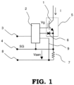
- FIG. 1 is a circuit diagram showing a schematic configuration of a power semiconductor element gate driving circuit according to Embodiment 1.
- a shunt resistor 7 is connected to an emitter terminal of a power semiconductor element 1 (also referred to as switch element 1).
- the potential of the emitter of the switch element 1, i.e., the potential of a reference potential terminal 4, is set as a reference potential (SG) of a drive control circuit 2.
- a diode 6 as a temperature sensor (also referred to as temperature sensor diode 6) for detecting a temperature of the switch element 1 is mounted on a chip 5 which is the same as that for the switch element 1.
- Collector current I flowing through the switch element 1 is converted into a voltage by the shunt resistor 7, and a voltage across the shunt resistor 7 (a voltage relative to a reference potential SG; hereinafter, Vsen) is inputted to the drive control circuit 2.
- Vsen a voltage across the shunt resistor 7
- the switch element 1 is not limited to an IGBT and may be a switch element having a gate electrode, such as a power transistor or an MOSFET.
- a voltage value relative to the reference potential SG is inputted as a temperature detection value of the switch element 1, and a voltage value relative to the reference potential SG is inputted as a current detection value of main current of the switch element 1.
- the temperature detection value is inputted as a positive voltage value relative to the reference potential, and the current detection value is inputted as a negative voltage value relative to the reference potential.
- the temperature detection value is, as described later, a positive voltage value that decreases in association with increase in the temperature
- the current detection value is a negative voltage value, an absolute value of which increases in association with increase in the current.
- FIG. 2 is a circuit diagram showing a detailed configuration of the power semiconductor element gate driving circuit according to Embodiment 1. This circuit is merely an example, and only parts related to the present invention are shown in FIG. 2 .
- a third differential amplifier U3 controls gate current such that the gate electrode of the switch element 1 is charged with electric charges and the electric charges are discharged, whereby ON/OFF control is performed on the collector current I which is main current flowing through the switch element 1.
- a first differential amplifier U1 receives a voltage drop Vf having occurred in the temperature sensor diode 6 and Vsen of the shunt resistor 7, amplifies a difference voltage between Vf and Vsen, and outputs the resultant voltage.
- Vf is inputted to a non-inversion input terminal of the first differential amplifier U1 as a positive voltage relative to the reference potential SG
- Vsen is inputted to an inversion input terminal of the first differential amplifier U1 as a negative voltage relative to the reference potential SG, and a voltage proportional to the difference between these voltages is outputted.
- a Zener diode D3 connected to the output side of the first differential amplifier U1 is provided for performing offset adjustment on the output voltage from the first differential amplifier U1.
- the breakdown voltage of the Zener diode D3 has a temperature characteristic.
- the Zener diode D3 is configured to, by being disposed at a position under an environment with the same temperature as the temperature of heat dissipation fins to which the drive control circuit 2 or the switch element 1 is connected, adjust an offset voltage according to the magnitude of the temperature.
- a second differential amplifier U2 outputs, as a voltage V2_, a voltage difference between a voltage V1 generated by a constant voltage control element D7 which is, for example, a Zener diode and a voltage V1_ obtained through the offset adjustment performed, by the Zener diode D3, on the output voltage from the first differential amplifier U1.
- the constant voltage control element D7 is also configured to, by being disposed at a position under a temperature condition equivalent to a temperature condition for the Zener diode D3, control the magnitude of the voltage V1 according to the temperature.
- the output side of the second differential amplifier U2 is connected to a non-inversion input terminal of the third differential amplifier U3 with a resistor R2 interposed therebetween.
- the non-inversion input terminal of the third differential amplifier U3 is further connected to a gate signal terminal 3 with a diode D6 interposed therebetween. To the gate signal terminal 3, gate signals for turning on and off the switch element 1 are inputted.
- an ON signal has a low level
- an OFF signal has a high level. Therefore, when an ON signal is inputted to the gate signal terminal 3, the diode D6 is turned on, whereby the potential Vset of the non-inversion input terminal of the third differential amplifier U3 comes to have the low level. Meanwhile, if an OFF signal is inputted to the gate signal terminal 3, the diode D6 is turned off, whereby the potential Vset becomes the potential of V2_.
- the forward-direction voltage drop Vf of the temperature sensor diode 6 has a characteristic of decreasing in association with increase in the temperature of the element.
- the temperature sensor diode 6 is configured to allow current to flow thereto via a constant current diode D2.
- Vf is inputted to the non-inversion input terminal of the first differential amplifier U1 so as not to cause any error in current of the constant current diode D2.
- V 1_ A ⁇ Vf ⁇ Vz
- the second differential amplifier U2 amplifies the difference between the reference voltage V1 and V1_, to obtain the output V2_ which is represented by the following expression.
- V2_ determined according to Expression (2) increases in association with increase in the temperature as shown in FIG. 3 .
- the second differential amplifier U2 is formed as an amplifier configured to adjust an offset when amplifying the difference between V1 and V1_.
- FIG. 3 shows a case where offset adjustment is performed such that the output V2_ becomes equal to V1 when V1 and V1_ match.
- the offset is preferably adjusted so as to obtain an advantageous effect on the basis of characteristics of the switch element 1, the temperature sensor diode 6, or the like.
- the second differential amplifier U2 only has to have a function of being able to adjust the offset to the difference between V1 and V1_, and thus is not limited to a differential amplifier and may be implemented by a subtraction circuit capable of offset adjustment.
- the third differential amplifier U3 adjusts a gate voltage of a transistor J1 such that a voltage drop in a sensing resistor R1 becomes equal to Vset.
- gate current in an OFF state is controlled to increase in association with increase in the temperature and is adjusted to shorten an OFF period of the switch element 1.
- Vset is adjusted to increase according to an output from a comparator U4 if Vf becomes equal to or lower than V2 as a result of increase in the temperature. It is noted that a pull-up resistor R6 and a diode D5 are connected to the output side of the comparator U4 such that, when Vf is higher than V2, i.e., the temperature is lower than a temperature T1, an output from the comparator U4 does not influence the voltage Vset.
- the third differential amplifier U3 adjusts a gate voltage of the transistor J1 such that Vset and a voltage drop based on gate current in the sensing resistor R1 become equal to each other. Consequently, the gate current in an OFF state increases in association with increase in the temperature. Thus, control is performed such that: a temperature characteristic of the OFF period of the switch element 1 is canceled out; and the switching time does not significantly change even upon change in the temperature.
- control is performed such that, according to the output from the comparator U4, the gate current is forcedly increased and a switching time in an OFF state is further shortened, in order to reduce loss in the switch element 1.
- the purpose of this control is to perform protection in cases of occurrence of deficiency in a dead time, such as a case where load current suddenly changes at a temperature higher than T1.
- this control is performed in order to eliminate a short circuit in a short period in the case of a sudden change in load current, by performing an operation with a shorter time constant than the time constant in control that is performed at a temperature lower than the temperature T1 and that involves changing the gate current in association with change in the temperature.
- this circuit makes it possible to reduce switching loss when the temperature becomes equal to or higher than T1. Thus, further increase in the temperature of the switch element 1 can also be inhibited.
- the output from the comparator U4 can also be outputted to outside as a temperature abnormality signal for protecting the switch element 1 from being heated.
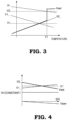
- FIG. 4 shows voltages of the respective portions with respect to collector current I.
- the switch element 1 has a characteristic that the mirror voltage of the switch element 1 decreases when the collector current I at the time of switching decreases. Consequently, the potential difference between the mirror voltage in an OFF state and an output Vg for a gate electrode of the drive control circuit 2 in an OFF state decreases, and mirror current decreases. Thus, dVce/dt at the time of switching decreases. Therefore, if the gate voltage is controlled with a constant voltage in an OFF state, when the collector current I is small, the difference between a mirror potential Vm and the potential of a negative power supply decreases, and mirror current decreases.
- the shunt resistor 7 in FIG. 2 performs detection, based on the collector current I, as the detection voltage Vsen having a negative sign relative to the reference potential SG, a difference between Vsen and the voltage drop Vf in the temperature sensor diode 6 is obtained, and the first differential amplifier U1 amplifies the difference.
- control is performed such that: Vset decreases; and the gate current in an OFF state decreases. That is, in a state where the switch element 1 is OFF, control is performed such that the gate current (mirror current) is larger at the time of interrupting small collector current than at the time of interrupting large collector current.
- Vset decreases
- the gate current in an OFF state decreases. That is, in a state where the switch element 1 is OFF, control is performed such that the gate current (mirror current) is larger at the time of interrupting small collector current than at the time of interrupting large collector current.
- control is performed so as to reduce, according to the magnitude of the collector current, a change in a period from a time at which the gate signal from the gate signal terminal 3 is changed to an OFF signal to a time at which the switch element 1 is turned off, i.e., to a time at which a mirror period ends.
- control is performed such that the gate current for discharging the electric charges from the gate electrode of the switch element 1 when the gate signal is changed to an OFF signal increases in association with increase in the temperature of the switch element 1 and decreases in association with increase in the collector current.
- the gate current is controlled on the basis of the difference between the temperature detection value of the switch element 1 and the current detection value of the collector current.
- the temperature detection value is inputted to the non-inversion input terminal of the first differential amplifier U1 as a positive voltage that decreases in association with increase in the temperature
- the current detection value is inputted to the inversion input terminal of the first differential amplifier U1 as a negative voltage, the absolute value of which increases in association with increase in the current
- the gate current is controlled on the basis of the output from the first differential amplifier U1.
- a power semiconductor element having a gate electrode is such that, under a switching condition that the temperature of the element is high and the collector current is small, the mirror potential at the time of switching becomes low, and a period from a time at which the gate signal is switched to an OFF signal to a time at which switching is ended is elongated.
- control is performed such that the gate current increases at high temperature and increases at small collector current.
- a delay of the switching time in an OFF state particularly decreases. Therefore, an operation is performed such that change, in the switching time, based on change in the temperature and change in the collector current is little. As a result, a power semiconductor element gate driving circuit capable of shortening a dead time can be provided.
- circuits are formed as analog circuits such as the differential amplifiers in the present embodiment, the circuits are not limited to analog circuits and may be formed as digital circuits for controlling the gate current in an OFF state on the basis of the difference between the temperature detection value and the current detection value.
- a configuration may be employed in which: each detection value is detected as a voltage value relative to the reference potential; and the reference potential is adjusted according to an ambient temperature or the temperature of heat dissipation fins mounted with the switch element.
- the control circuit Since the gate current in an OFF state is controlled on the basis of the difference between the temperature detection value and the current detection value regardless of whether an analog circuit or a digital circuit is used, the control circuit is not formed as a complicated one that switches a resistance. Thus, it is possible to provide, by means of a simple configuration, a power semiconductor element gate driving circuit in which: the switching time in an OFF state changes only a little; and the dead time can be shortened.
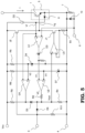
- FIG. 5 is a circuit diagram showing a power semiconductor element gate driving circuit according to Embodiment 2.
- a diode 10 is connected in parallel to the shunt resistor 7.
- the other components are the same as those in Embodiment 1.
- the gate current, in an OFF state, of the switch element 1 is controlled to decrease in association with increase in the collector current.
- Vth changes significantly upon a change within a region in which the collector current is small, but Vth changes less at a larger collector current.
- the diode 10 is connected in parallel to the shunt resistor 7 such that the magnitude of Vsen does not significantly change within the region in which the collector current I is large.
- a Zener diode may be connected instead of the diode 10, with an anode and a cathode being inverted.
- FIG. 6 shows changes in voltages of the respective portions with respect to collector current I.
- description will be given by taking, as an example, a case where the switch element 1 has a characteristic that a voltage drop that occurs in a parallel unit composed of the shunt resistor 7 and the diode 10 hardly changes within a region in which the collector current I is equal to or larger than 1 A.
- the resistance value of the shunt resistor 7 and characteristics of the diode 10 are set such that the voltage value of the voltage drop having occurred at the shunt resistor 7 when a current of 1 A flows through the shunt resistor 7, becomes equal to a threshold voltage of the diode 10.
- Vsen increases to the negative side from the reference potential in proportion to current.
- adjustment is performed such that, in this current region, V1_ increases and V2_ decreases in association with increase in the current value.
- the third differential amplifier U3 performs control such that the current flowing through the sensing resistor R1, i.e., the gate current in an OFF state, decreases.
- the collector current I flows through the diode 10, and thus Vsen becomes equal to the threshold voltage of the diode 10 and hardly changes.
- control can be performed such that the gate current in an OFF state decreases in association with increase in the collector current only when the collector current I is equal to or smaller than a predetermined value.
- Constants in the circuits in FIG. 5 only have to be adjusted according to characteristics of the switch element 1 and the temperature sensor diode 6 which are targets.
- FIG. 7 is a circuit diagram showing a power semiconductor element gate driving circuit according to Embodiment 3.
- Embodiment 1 and Embodiment 2 description has been given regarding a configuration in which the total collector current I of the switch element 1 is set to flow through the shunt resistor 7 or the diode so that the collector current is detected. In this case, losses in the shunt resistor 7 and the diode 10 increase when large collector current flows.
- a power semiconductor element provided with a sensing cell 11 is used as the switch element 1 as shown in FIG. 7 .
- current flowing through the sensing cell 11 is detected by the shunt resistor 7. Consequently, loss in the shunt resistor 7 caused by the current of the switch element 1 can be reduced.
- a cathode of the temperature sensor diode 6 is connected to an emitter of the sensing cell 11 so that influence of Vsen is not inflicted on Vf. Current division among chips for the switch element 1 is adjusted according to a gate resistance provided in the switch element 1.
- the current flowing through the switch element 1 flows in proportion to the cell effective areas of the entire switch element 1 and the sensing cell 11.
- the total collector current flowing through the switch element 1 can be ascertained from: the current flowing through the shunt resistor 7; and the proportion of the cell effective area of the sensing cell 11 to the cell effective area of the entire switch element 1.
- a current division ratio of the sensing cell 11 may also be ascertained through a test.
- a collector current of the sensing cell 11 makes it possible to adjust the gate current according to the value of the collector current as described in embodiments 1 and 2, without measuring the total current of the switch element 1.
- a configuration in which the Zener diode 10 is connected in parallel to the shunt resistor 7 is employed in FIG. 7 , and this configuration can limit an upper limit value of Vsen in the same manner as that described in Embodiment 2.
- a collector current value can be detected without passage, through the shunt resistor 7, of the total collector current I flowing through the switch element 1.
- the switching time can be controlled by detecting the magnitude of the collector current I with only a small loss.
Landscapes
- Engineering & Computer Science (AREA)
- Power Engineering (AREA)
- Power Conversion In General (AREA)
- Electronic Switches (AREA)
Abstract
Description
- The present invention relates to a power semiconductor element gate driving circuit.
- In general, a power conversion device performs power conversion between DC and AC through ON/OFF switching of main current of a power semiconductor element such as an IGBT or an MOSFET by charging a gate electrode of the power semiconductor element with electric charges and discharging the electric charges.
- In general, characteristics of the semiconductor element change according to the temperature thereof. Considering this, various countermeasures have been proposed. The countermeasures are intended to compensate for temperature characteristics of a power semiconductor element in a gate driving circuit in which a gate electrode of the power semiconductor element is charged with electric charges and the electric charges are discharged, i.e., gate current is controlled.
- For example,
Patent Document 1 proposes a technology of detecting a temperature of a power semiconductor element and switching a gate resistance in an OFF state, in order to adjust gate current of the power semiconductor element according to change in a temperature condition or the like. In the case of this configuration, a control circuit for switching the gate resistance in stages is complicated. - In addition, a gate driving circuit in which both reduction in switching loss and reduction in switching noise can be automatically achieved even upon change in temperature, has been disclosed (Patent Document 2). In
Patent Document 2, noise at the time of switching is reduced by adjusting gate current flowing while a power semiconductor element is ON. In the case of configuring a switching power supply such as an inverter, two power semiconductor elements are sometimes connected in series. In the configuration disclosed inPatent Document 2, both reduction in switching loss and reduction in switching noise can be achieved. However, in consideration of a time at which a switching time becomes longest in an operation-possible temperature region for the power semiconductor elements, a dead time needs to be provided such that the two power semiconductor elements connected in series are not simultaneously turned on. - The dead time is a time of limiting a conduction period for each of the elements and inflicts influences such as: occurrence of distortion of a waveform outputted from the switching power supply; and occurrence of voltage fluctuation. These influences cause a greater error in the case of a power supply with a high switching frequency and a short switching cycle, such as a power supply in which a wide-bandgap semiconductor element is used as a power semiconductor element.
- Further,
Patent Document 3 describes a configuration in which a current threshold value at which a gate resistance is switched is changed according to a temperature. InPatent Document 3, control of a power semiconductor element in an ON state is mainly contemplated, and a technology of discontinuously adjusting a switching speed through complicated control as in switching of the gate resistance has been disclosed. Moreover, inPatent Document 3, when current is small, a switching time in an OFF state is particularly elongated, and a dead time is limited by the switching time in an OFF state. Thus, a long dead time is necessary. - Patent Document 1: Japanese Laid-Open Patent Publication
JP 2002- 119 044 - Patent Document 2:
WO2014/123046 A1 - Patent Document 3: Japanese Laid-Open Patent Publication
JP 2008- 182 835 A - As described above, conventionally, control with a focus placed on switching loss or a switching time in an ON state has been mainly contemplated, and contemplation on shortening a dead time in consideration of a switching time in an OFF state as well has not been conducted. In a constant-voltage drive circuit, for a power semiconductor element, that performs switching by charging a gate electrode with electric charges and discharging the electric charges, increase in the temperature of the element leads to reduction in a mirror potential so that a delay period taken to arrival at a switching time is elongated particularly at the time of switching in an OFF state.
- Further, increase in the temperature of the element leads to reduction in mirror current during constant-voltage drive. Thus, dVce/dt at the time of switching is reduced, and a period from input of an OFF signal for switching to end of the switching is elongated. Therefore, a long dead time needs to be set. This dead time causes an error in a power supply output and causes trouble during switching at a high frequency.
- The present invention has been made to solve the above problems, and an object of the present invention is to, with a focus placed on a switching time in an OFF state, provide a power semiconductor element gate driving circuit in which: the switching time in an OFF state changes only a little even upon change in the temperature of a power semiconductor element and change in a current value; and a dead time can be shortened.
- A power semiconductor element gate driving circuit according to the present invention is a power semiconductor element gate driving circuit that performs ON/OFF control on main current of a power semiconductor element having a gate electrode by charging the gate electrode of the power semiconductor element with electric charges and discharging the electric charges on the basis of an inputted gate signal. When the gate signal is switched to an OFF signal, control is performed such that gate current for discharging the electric charges from the gate electrode increases in association with increase in a temperature of the power semiconductor element and decreases in association with increase in the main current.
- The power semiconductor element gate driving circuit according to the present invention has an advantageous effect of: being able to make setting such that a switching time in an OFF state changes only a little even upon change in temperature and change in current; and being able to shorten a necessary dead time.
-
-
FIG. 1 is a circuit diagram showing a schematic configuration of a power semiconductor element gate driving circuit according toEmbodiment 1. -
FIG. 2 is a circuit diagram showing a detailed configuration of the power semiconductor element gate driving circuit according toEmbodiment 1. -
FIG. 3 is a graph for explaining an operation based on change in temperature, in the power semiconductor element gate driving circuit according toEmbodiment 1. -
FIG. 4 is a graph for explaining an operation based on change in collector current of a power semiconductor element, in the power semiconductor element gate driving circuit according toEmbodiment 1. -
FIG. 5 is a circuit diagram showing a detailed configuration of a power semiconductor element gate driving circuit according toEmbodiment 2. -
FIG. 6 is a graph for explaining an operation based on change in the collector current of the power semiconductor element, in the power semiconductor element gate driving circuit according toEmbodiment 2. -
FIG. 7 is a circuit diagram showing a detailed configuration of a power semiconductor element gate driving circuit according toEmbodiment 3. -
FIG. 1 is a circuit diagram showing a schematic configuration of a power semiconductor element gate driving circuit according toEmbodiment 1. Ashunt resistor 7 is connected to an emitter terminal of a power semiconductor element 1 (also referred to as switch element 1). The potential of the emitter of theswitch element 1, i.e., the potential of a referencepotential terminal 4, is set as a reference potential (SG) of adrive control circuit 2. Adiode 6 as a temperature sensor (also referred to as temperature sensor diode 6) for detecting a temperature of theswitch element 1 is mounted on achip 5 which is the same as that for theswitch element 1. - An output wire to which a load such as a power supply for supplying power, a capacitor, or a motor is connected, is connected to a
terminal 8 on an opposite side, of theshunt resistor 7, to the emitter terminal. Collector current I flowing through theswitch element 1 is converted into a voltage by theshunt resistor 7, and a voltage across the shunt resistor 7 (a voltage relative to a reference potential SG; hereinafter, Vsen) is inputted to thedrive control circuit 2. It is noted that, although an IGBT is assumed as theswitch element 1 in the present embodiment, theswitch element 1 is not limited to an IGBT and may be a switch element having a gate electrode, such as a power transistor or an MOSFET. - As described above, to the
drive control circuit 2, a voltage value relative to the reference potential SG is inputted as a temperature detection value of theswitch element 1, and a voltage value relative to the reference potential SG is inputted as a current detection value of main current of theswitch element 1. The temperature detection value is inputted as a positive voltage value relative to the reference potential, and the current detection value is inputted as a negative voltage value relative to the reference potential. - The temperature detection value is, as described later, a positive voltage value that decreases in association with increase in the temperature, and the current detection value is a negative voltage value, an absolute value of which increases in association with increase in the current.
-
FIG. 2 is a circuit diagram showing a detailed configuration of the power semiconductor element gate driving circuit according toEmbodiment 1. This circuit is merely an example, and only parts related to the present invention are shown inFIG. 2 . In the circuit inFIG. 2 , a third differential amplifier U3 controls gate current such that the gate electrode of theswitch element 1 is charged with electric charges and the electric charges are discharged, whereby ON/OFF control is performed on the collector current I which is main current flowing through theswitch element 1. - A first differential amplifier U1 receives a voltage drop Vf having occurred in the
temperature sensor diode 6 and Vsen of theshunt resistor 7, amplifies a difference voltage between Vf and Vsen, and outputs the resultant voltage. Vf is inputted to a non-inversion input terminal of the first differential amplifier U1 as a positive voltage relative to the reference potential SG, Vsen is inputted to an inversion input terminal of the first differential amplifier U1 as a negative voltage relative to the reference potential SG, and a voltage proportional to the difference between these voltages is outputted. - A Zener diode D3 connected to the output side of the first differential amplifier U1 is provided for performing offset adjustment on the output voltage from the first differential amplifier U1. The breakdown voltage of the Zener diode D3 has a temperature characteristic. The Zener diode D3 is configured to, by being disposed at a position under an environment with the same temperature as the temperature of heat dissipation fins to which the
drive control circuit 2 or theswitch element 1 is connected, adjust an offset voltage according to the magnitude of the temperature. - A second differential amplifier U2 outputs, as a voltage V2_, a voltage difference between a voltage V1 generated by a constant voltage control element D7 which is, for example, a Zener diode and a voltage V1_ obtained through the offset adjustment performed, by the Zener diode D3, on the output voltage from the first differential amplifier U1. The constant voltage control element D7 is also configured to, by being disposed at a position under a temperature condition equivalent to a temperature condition for the Zener diode D3, control the magnitude of the voltage V1 according to the temperature.
- The output side of the second differential amplifier U2 is connected to a non-inversion input terminal of the third differential amplifier U3 with a resistor R2 interposed therebetween. The non-inversion input terminal of the third differential amplifier U3 is further connected to a
gate signal terminal 3 with a diode D6 interposed therebetween. To thegate signal terminal 3, gate signals for turning on and off theswitch element 1 are inputted. - Out of the gate signals inputted to the
gate signal terminal 3, an ON signal has a low level, and an OFF signal has a high level. Therefore, when an ON signal is inputted to thegate signal terminal 3, the diode D6 is turned on, whereby the potential Vset of the non-inversion input terminal of the third differential amplifier U3 comes to have the low level. Meanwhile, if an OFF signal is inputted to thegate signal terminal 3, the diode D6 is turned off, whereby the potential Vset becomes the potential of V2_. - Hereinafter, an operation performed when the gate signal is changed to an OFF signal, i.e., in an OFF state where electric charges are discharged from the gate electrode of the
switch element 1, will be described. Firstly, an operation, in an OFF state, of the power semiconductor element gate driving circuit shown inFIG. 2 upon change in the temperature will be described with reference toFIG. 3 showing voltages of the respective portions with respect to the temperature. - In the following descriptions, the operation upon change in the temperature will be explained, and thus the descriptions will be given with the voltage drop Vsen in the
shunt resistor 7 being excluded under a condition that: the collector current of theswitch element 1 is fixed; and Vsen is fixed. The forward-direction voltage drop Vf of thetemperature sensor diode 6 has a characteristic of decreasing in association with increase in the temperature of the element. Thetemperature sensor diode 6 is configured to allow current to flow thereto via a constant current diode D2. Vf is inputted to the non-inversion input terminal of the first differential amplifier U1 so as not to cause any error in current of the constant current diode D2. If an amplification factor in the first differential amplifier U1 is defined as A, and a voltage drop in the Zener diode D3 is defined as Vz, the potential V1_ of an inversion input terminal of the second differential amplifier U2 is represented by the following expression.
- The second differential amplifier U2 amplifies the difference between the reference voltage V1 and V1_, to obtain the output V2_ which is represented by the following expression.

- V2_ determined according to Expression (2) increases in association with increase in the temperature as shown in
FIG. 3 . In actuality, the second differential amplifier U2 is formed as an amplifier configured to adjust an offset when amplifying the difference between V1 and V1_.FIG. 3 shows a case where offset adjustment is performed such that the output V2_ becomes equal to V1 when V1 and V1_ match. The offset is preferably adjusted so as to obtain an advantageous effect on the basis of characteristics of theswitch element 1, thetemperature sensor diode 6, or the like. - The second differential amplifier U2 only has to have a function of being able to adjust the offset to the difference between V1 and V1_, and thus is not limited to a differential amplifier and may be implemented by a subtraction circuit capable of offset adjustment. In an OFF state, the third differential amplifier U3 adjusts a gate voltage of a transistor J1 such that a voltage drop in a sensing resistor R1 becomes equal to Vset.
- Therefore, gate current in an OFF state is controlled to increase in association with increase in the temperature and is adjusted to shorten an OFF period of the
switch element 1. In addition, Vset is adjusted to increase according to an output from a comparator U4 if Vf becomes equal to or lower than V2 as a result of increase in the temperature. It is noted that a pull-up resistor R6 and a diode D5 are connected to the output side of the comparator U4 such that, when Vf is higher than V2, i.e., the temperature is lower than a temperature T1, an output from the comparator U4 does not influence the voltage Vset. - The third differential amplifier U3 adjusts a gate voltage of the transistor J1 such that Vset and a voltage drop based on gate current in the sensing resistor R1 become equal to each other. Consequently, the gate current in an OFF state increases in association with increase in the temperature. Thus, control is performed such that: a temperature characteristic of the OFF period of the
switch element 1 is canceled out; and the switching time does not significantly change even upon change in the temperature. - When the temperature of the
switch element 1 exceeds T1, control is performed such that, according to the output from the comparator U4, the gate current is forcedly increased and a switching time in an OFF state is further shortened, in order to reduce loss in theswitch element 1. The purpose of this control is to perform protection in cases of occurrence of deficiency in a dead time, such as a case where load current suddenly changes at a temperature higher than T1. - Specifically, this control is performed in order to eliminate a short circuit in a short period in the case of a sudden change in load current, by performing an operation with a shorter time constant than the time constant in control that is performed at a temperature lower than the temperature T1 and that involves changing the gate current in association with change in the temperature. In addition, this circuit makes it possible to reduce switching loss when the temperature becomes equal to or higher than T1. Thus, further increase in the temperature of the
switch element 1 can also be inhibited. In addition, the output from the comparator U4 can also be outputted to outside as a temperature abnormality signal for protecting theswitch element 1 from being heated. - Next, the feature of automatically controlling a change, in the switching time in an OFF state, based on a change in the collector current I of the
switch element 1 will be described.FIG. 4 shows voltages of the respective portions with respect to collector current I. In order to facilitate understanding of descriptions, explanations will be given under a condition that the temperature of theswitch element 1 does not change, i.e., a condition that Vf is fixed. - The
switch element 1 has a characteristic that the mirror voltage of theswitch element 1 decreases when the collector current I at the time of switching decreases. Consequently, the potential difference between the mirror voltage in an OFF state and an output Vg for a gate electrode of thedrive control circuit 2 in an OFF state decreases, and mirror current decreases. Thus, dVce/dt at the time of switching decreases. Therefore, if the gate voltage is controlled with a constant voltage in an OFF state, when the collector current I is small, the difference between a mirror potential Vm and the potential of a negative power supply decreases, and mirror current decreases. - This leads to decrease in dVce/dt and elongation of the switching period. This phenomenon prominently occurs not only in the case in the present embodiment but also in the case of using no negative bias for the drive circuit or the case of using an element having a low threshold potential. In the present embodiment, in order not to elongate the switching period at a small collector current I, the
shunt resistor 7 inFIG. 2 performs detection, based on the collector current I, as the detection voltage Vsen having a negative sign relative to the reference potential SG, a difference between Vsen and the voltage drop Vf in thetemperature sensor diode 6 is obtained, and the first differential amplifier U1 amplifies the difference. - Change in the switching time upon change in the collector current I will be described with reference to
FIG. 4 . When the collector current I increases, the difference between Vf and Vsen increases in the first differential amplifier U1 so that the voltage V1_ increases. When V1_ increases, the output voltage V2_ from the second differential amplifier U2 which amplifies the difference between V1 and V1_ decreases. - Consequently, control is performed such that: Vset decreases; and the gate current in an OFF state decreases. That is, in a state where the
switch element 1 is OFF, control is performed such that the gate current (mirror current) is larger at the time of interrupting small collector current than at the time of interrupting large collector current. Thus, even if the collector current of theswitch element 1 changes, a period that Vge takes to reach the mirror potential can be shortened. - Consequently, control is performed so as to reduce, according to the magnitude of the collector current, a change in a period from a time at which the gate signal from the
gate signal terminal 3 is changed to an OFF signal to a time at which theswitch element 1 is turned off, i.e., to a time at which a mirror period ends. - As described above, control is performed such that the gate current for discharging the electric charges from the gate electrode of the
switch element 1 when the gate signal is changed to an OFF signal increases in association with increase in the temperature of theswitch element 1 and decreases in association with increase in the collector current. - More specifically, the gate current is controlled on the basis of the difference between the temperature detection value of the
switch element 1 and the current detection value of the collector current. In one example of realizing this control, the temperature detection value is inputted to the non-inversion input terminal of the first differential amplifier U1 as a positive voltage that decreases in association with increase in the temperature, the current detection value is inputted to the inversion input terminal of the first differential amplifier U1 as a negative voltage, the absolute value of which increases in association with increase in the current, and the gate current is controlled on the basis of the output from the first differential amplifier U1. - In general, a power semiconductor element having a gate electrode is such that, under a switching condition that the temperature of the element is high and the collector current is small, the mirror potential at the time of switching becomes low, and a period from a time at which the gate signal is switched to an OFF signal to a time at which switching is ended is elongated. In the gate driving circuit according to the
present Embodiment 1, control is performed such that the gate current increases at high temperature and increases at small collector current. - Consequently, a delay of the switching time in an OFF state particularly decreases. Therefore, an operation is performed such that change, in the switching time, based on change in the temperature and change in the collector current is little. As a result, a power semiconductor element gate driving circuit capable of shortening a dead time can be provided.
- Although the circuits are formed as analog circuits such as the differential amplifiers in the present embodiment, the circuits are not limited to analog circuits and may be formed as digital circuits for controlling the gate current in an OFF state on the basis of the difference between the temperature detection value and the current detection value. In this case, a configuration may be employed in which: each detection value is detected as a voltage value relative to the reference potential; and the reference potential is adjusted according to an ambient temperature or the temperature of heat dissipation fins mounted with the switch element.
- Since the gate current in an OFF state is controlled on the basis of the difference between the temperature detection value and the current detection value regardless of whether an analog circuit or a digital circuit is used, the control circuit is not formed as a complicated one that switches a resistance. Thus, it is possible to provide, by means of a simple configuration, a power semiconductor element gate driving circuit in which: the switching time in an OFF state changes only a little; and the dead time can be shortened.
-
FIG. 5 is a circuit diagram showing a power semiconductor element gate driving circuit according toEmbodiment 2. A difference fromEmbodiment 1 is that adiode 10 is connected in parallel to theshunt resistor 7. The other components are the same as those inEmbodiment 1. InEmbodiment 1, the gate current, in an OFF state, of theswitch element 1 is controlled to decrease in association with increase in the collector current. In the case where theswitch element 1 is an IGBT, Vth changes significantly upon a change within a region in which the collector current is small, but Vth changes less at a larger collector current. - Further, within a region in which the collector current is large, a delay of the OFF period might increase more than necessary in association with increase in the temperature. In such a case, adverse influence might be inflicted with only the control described in
Embodiment 1. In order to suppress the adverse influence, current flowing through theshunt resistor 7 is limited. To this end, thediode 10 is connected in parallel to theshunt resistor 7 such that the magnitude of Vsen does not significantly change within the region in which the collector current I is large. Although a configuration in which thediode 10 is connected in parallel to theshunt resistor 7 is shown inFIG. 5 as a configuration for limiting Vsen, a Zener diode may be connected instead of thediode 10, with an anode and a cathode being inverted. -
FIG. 6 shows changes in voltages of the respective portions with respect to collector current I. With reference toFIG. 6 , description will be given by taking, as an example, a case where theswitch element 1 has a characteristic that a voltage drop that occurs in a parallel unit composed of theshunt resistor 7 and thediode 10 hardly changes within a region in which the collector current I is equal to or larger than 1 A. - The resistance value of the
shunt resistor 7 and characteristics of thediode 10 are set such that the voltage value of the voltage drop having occurred at theshunt resistor 7 when a current of 1 A flows through theshunt resistor 7, becomes equal to a threshold voltage of thediode 10. By this setting, most of the collector current I flows through theshunt resistor 7 within a region in which the collector current is equal to or smaller than 1 A. - Thus, the magnitude of Vsen increases to the negative side from the reference potential in proportion to current. As a result, adjustment is performed such that, in this current region, V1_ increases and V2_ decreases in association with increase in the current value. If V2_ decreases, the third differential amplifier U3 performs control such that the current flowing through the sensing resistor R1, i.e., the gate current in an OFF state, decreases. Within the current region in which the collector current I is equal to or larger than 1 A, the collector current I flows through the
diode 10, and thus Vsen becomes equal to the threshold voltage of thediode 10 and hardly changes. - If the diode is provided in parallel to the
shunt resistor 7 so as to limit the maximum value of Vsen in this manner, control can be performed such that the gate current in an OFF state decreases in association with increase in the collector current only when the collector current I is equal to or smaller than a predetermined value. - Meanwhile, when the collector current is equal to or larger than the predetermined value, further decrease in the gate current can be prevented, and the delay of the OFF period can be prevented from increasing. Constants in the circuits in
FIG. 5 only have to be adjusted according to characteristics of theswitch element 1 and thetemperature sensor diode 6 which are targets. -
FIG. 7 is a circuit diagram showing a power semiconductor element gate driving circuit according toEmbodiment 3. InEmbodiment 1 andEmbodiment 2, description has been given regarding a configuration in which the total collector current I of theswitch element 1 is set to flow through theshunt resistor 7 or the diode so that the collector current is detected. In this case, losses in theshunt resistor 7 and thediode 10 increase when large collector current flows. - In
Embodiment 3, a power semiconductor element provided with a sensingcell 11 is used as theswitch element 1 as shown inFIG. 7 . In thepresent Embodiment 3, current flowing through the sensingcell 11 is detected by theshunt resistor 7. Consequently, loss in theshunt resistor 7 caused by the current of theswitch element 1 can be reduced. A cathode of thetemperature sensor diode 6 is connected to an emitter of the sensingcell 11 so that influence of Vsen is not inflicted on Vf. Current division among chips for theswitch element 1 is adjusted according to a gate resistance provided in theswitch element 1. - With this configuration, the current flowing through the
switch element 1 flows in proportion to the cell effective areas of theentire switch element 1 and the sensingcell 11. Thus, the total collector current flowing through theswitch element 1 can be ascertained from: the current flowing through theshunt resistor 7; and the proportion of the cell effective area of the sensingcell 11 to the cell effective area of theentire switch element 1. Alternatively, a current division ratio of the sensingcell 11 may also be ascertained through a test. - Therefore, detection of a collector current of the sensing
cell 11 makes it possible to adjust the gate current according to the value of the collector current as described inembodiments switch element 1. A configuration in which theZener diode 10 is connected in parallel to theshunt resistor 7 is employed inFIG. 7 , and this configuration can limit an upper limit value of Vsen in the same manner as that described inEmbodiment 2. With the above configuration, a collector current value can be detected without passage, through theshunt resistor 7, of the total collector current I flowing through theswitch element 1. Thus, the switching time can be controlled by detecting the magnitude of the collector current I with only a small loss. - Although various exemplary embodiments and examples are described in the present application, various features, aspects, and functions described in one or more embodiments are not inherent in a particular embodiment, and can be applicable alone or in their various combinations to each embodiment. Accordingly, countless variations that are not illustrated are envisaged within the scope of the art disclosed herein. For example, the case where at least one component is modified, added or omitted, and the case where at least one component is extracted and combined with a component in another embodiment are included.
-
- 1
- power semiconductor element
- 2
- drive control circuit
- 3
- gate signal terminal
- 4
- reference potential terminal
- 6
- diode (temperature sensor diode)
- 7
- shunt resistor
- 10
- diode
- U1
- first differential amplifier
- U2
- second differential amplifier
Claims (9)
- A power semiconductor element gate driving circuit that performs ON/OFF control on main current of a power semiconductor element having a gate electrode by charging the gate electrode of the power semiconductor element with electric charges and discharging the electric charges on the basis of an inputted gate signal, wherein
when the gate signal is switched to an OFF signal, control is performed such that gate current for discharging the electric charges from the gate electrode increases in association with increase in a temperature of the power semiconductor element and decreases in association with increase in the main current. - The power semiconductor element gate driving circuit according to claim 1, wherein
when the gate signal is switched to the OFF signal, the gate current for discharging the electric charges from the gate electrode is controlled on the basis of a difference between a temperature detection value obtained by detecting the temperature of the power semiconductor element and a current detection value which is a detection value of the main current. - The power semiconductor element gate driving circuit according to claim 2, whereinthe temperature detection value and the current detection value are each a value detected as a voltage relative to a reference potential,the temperature detection value is a positive voltage that decreases in association with increase in the temperature, andthe current detection value is a negative voltage, an absolute value of which increases in association with increase in the main current.
- The power semiconductor element gate driving circuit according to claim 3, further comprising:a first differential amplifier havinga non-inversion input terminal to which the temperature detection value is inputted andan inversion input terminal to which the current detection value is inputted; anda second differential amplifier having an inversion input terminal to which an output from the first differential amplifier is inputted, whereinwhen the gate signal is switched to the OFF signal, the gate current for discharging the electric charges from the gate electrode is controlled on the basis of an output from the second differential amplifier.
- The power semiconductor element gate driving circuit according to claim 3 or 4, whereinthe temperature detection value is a voltage value across a diode serving as a temperature sensor, andthe current detection value is a voltage value across a shunt resistor which detects the main current.
- The power semiconductor element gate driving circuit according to claim 5, further comprising
a diode connected in parallel to the shunt resistor. - The power semiconductor element gate driving circuit according to claim 6, wherein
the diode connected in parallel to the shunt resistor is a Zener diode. - The power semiconductor element gate driving circuit according to any one of claims 5 to 7, whereinthe power semiconductor element includes a sensing cell, andthe shunt resistor is connected to the sensing cell.
- The power semiconductor element gate driving circuit according to any one of claims 1 to 8, wherein
when the gate signal is switched to the OFF signal, and the temperature of the power semiconductor element is equal to or higher than a predetermined temperature, the gate current for discharging the electric charges from the gate electrode is forcedly controlled to have a predetermined value.
Applications Claiming Priority (1)
| Application Number | Priority Date | Filing Date | Title |
|---|---|---|---|
| PCT/JP2020/027606 WO2022013998A1 (en) | 2020-07-16 | 2020-07-16 | Gate driving circuit for power semiconductor element |
Publications (3)
| Publication Number | Publication Date |
|---|---|
| EP4184771A1 true EP4184771A1 (en) | 2023-05-24 |
| EP4184771A4 EP4184771A4 (en) | 2023-11-01 |
| EP4184771B1 EP4184771B1 (en) | 2025-06-18 |
Family
ID=79554543
Family Applications (1)
| Application Number | Title | Priority Date | Filing Date |
|---|---|---|---|
| EP20945160.8A Active EP4184771B1 (en) | 2020-07-16 | 2020-07-16 | Gate driving circuit for power semiconductor element |
Country Status (6)
| Country | Link |
|---|---|
| US (1) | US12278553B2 (en) |
| EP (1) | EP4184771B1 (en) |
| JP (1) | JP7374328B2 (en) |
| KR (1) | KR102728899B1 (en) |
| CN (1) | CN116157986A (en) |
| WO (1) | WO2022013998A1 (en) |
Cited By (1)
| Publication number | Priority date | Publication date | Assignee | Title |
|---|---|---|---|---|
| EP4510107A4 (en) * | 2022-04-15 | 2025-05-21 | Panasonic Intellectual Property Management Co., Ltd. | INFORMATION PROCESSING METHOD, INFORMATION PROCESSING DEVICE, AND PROGRAM |
Families Citing this family (3)
| Publication number | Priority date | Publication date | Assignee | Title |
|---|---|---|---|---|
| US12143099B2 (en) * | 2020-08-28 | 2024-11-12 | Nissan Motor Co., Ltd. | Switching element driving method and switching element driving device |
| US12476632B2 (en) * | 2023-10-17 | 2025-11-18 | Tagore Technology, Inc. | Temperature-adaptive gate driver for GaN switch |
| WO2025173143A1 (en) * | 2024-02-14 | 2025-08-21 | Astemo株式会社 | Gate drive device and electric power conversion device |
Family Cites Families (14)
| Publication number | Priority date | Publication date | Assignee | Title |
|---|---|---|---|---|
| JP2002119044A (en) | 2000-10-12 | 2002-04-19 | Fuji Electric Co Ltd | Gate drive circuit for power semiconductor device |
| JP3089166U (en) * | 2002-04-09 | 2002-10-11 | 船井電機株式会社 | Switching power supply |
| JP2008067593A (en) * | 2006-08-08 | 2008-03-21 | Fuji Electric Device Technology Co Ltd | Insulated gate type semiconductor switch element gate drive circuit |
| JP5063124B2 (en) | 2007-01-25 | 2012-10-31 | 三菱電機株式会社 | Semiconductor device |
| JP4844653B2 (en) | 2009-07-20 | 2011-12-28 | 株式会社デンソー | Driving device for power switching element |
| JP5862434B2 (en) | 2012-04-10 | 2016-02-16 | 富士電機株式会社 | Power transistor drive circuit |
| US9461640B2 (en) | 2012-12-21 | 2016-10-04 | Mitsubishi Electric Corporation | Switching element drive circuit, power module, and automobile |
| EP2955825B1 (en) | 2013-02-08 | 2019-08-28 | Mitsubishi Electric Corporation | Gate driving circuit |
| JP5943868B2 (en) * | 2013-03-27 | 2016-07-05 | 三菱電機株式会社 | Semiconductor switching element gate drive circuit |
| JP6187428B2 (en) * | 2014-03-27 | 2017-08-30 | 株式会社デンソー | Drive device |
| US10491095B2 (en) * | 2014-10-06 | 2019-11-26 | Ford Global Technologies, Llc | Dynamic IGBT gate drive for vehicle traction inverters |
| JP6750360B2 (en) * | 2016-07-15 | 2020-09-02 | 富士電機株式会社 | Semiconductor device |
| DE102016217494A1 (en) | 2016-09-14 | 2018-03-15 | Siemens Aktiengesellschaft | Method for operating a converter and thereafter operating converter |
| US10611246B2 (en) * | 2017-03-29 | 2020-04-07 | Ford Global Technologies, Llc | Gate driver with temperature compensated turn-off |
-
2020
- 2020-07-16 US US17/927,893 patent/US12278553B2/en active Active
- 2020-07-16 CN CN202080104918.4A patent/CN116157986A/en active Pending
- 2020-07-16 EP EP20945160.8A patent/EP4184771B1/en active Active
- 2020-07-16 WO PCT/JP2020/027606 patent/WO2022013998A1/en not_active Ceased
- 2020-07-16 KR KR1020237000386A patent/KR102728899B1/en active Active
- 2020-07-16 JP JP2022536060A patent/JP7374328B2/en active Active
Cited By (1)
| Publication number | Priority date | Publication date | Assignee | Title |
|---|---|---|---|---|
| EP4510107A4 (en) * | 2022-04-15 | 2025-05-21 | Panasonic Intellectual Property Management Co., Ltd. | INFORMATION PROCESSING METHOD, INFORMATION PROCESSING DEVICE, AND PROGRAM |
Also Published As
| Publication number | Publication date |
|---|---|
| JPWO2022013998A1 (en) | 2022-01-20 |
| KR20230021094A (en) | 2023-02-13 |
| KR102728899B1 (en) | 2024-11-11 |
| EP4184771A4 (en) | 2023-11-01 |
| US20230208274A1 (en) | 2023-06-29 |
| JP7374328B2 (en) | 2023-11-06 |
| EP4184771B1 (en) | 2025-06-18 |
| CN116157986A (en) | 2023-05-23 |
| WO2022013998A1 (en) | 2022-01-20 |
| US12278553B2 (en) | 2025-04-15 |
Similar Documents
| Publication | Publication Date | Title |
|---|---|---|
| EP4184771B1 (en) | Gate driving circuit for power semiconductor element | |
| US10281941B2 (en) | Voltage generating circuit and overcurrent detecting circuit | |
| EP2955825B1 (en) | Gate driving circuit | |
| US11095283B2 (en) | Drive control apparatus for driving a switching element including a sense element | |
| US9722594B2 (en) | Drive device | |
| US9476916B2 (en) | Overcurrent detection apparatus and intelligent power module using same | |
| US10236677B2 (en) | Semiconductor device | |
| US20160211657A1 (en) | Semiconductor device | |
| US6967519B2 (en) | Drive circuit for a power semiconductor device | |
| US11196386B2 (en) | Operation amplification circuit and over-current protection method therefor | |
| US11575371B2 (en) | Semiconductor device | |
| US8717068B2 (en) | Drive unit for driving voltage-driven element | |
| US10586791B2 (en) | Adaptive thermal overshoot and current limiting protection for MOSFETs | |
| US20210242864A1 (en) | Switch circuit capable of overcurrent protection with small and simple circuit, and with simple operation, without affecting normal operation | |
| US20150372672A1 (en) | Power device drive circuit | |
| US11695409B2 (en) | Drive circuit of power semiconductor element | |
| CN113381386B (en) | Electrical switching system including constant power controller and related methods | |
| US12323135B2 (en) | High-side semiconductor switch with over-current protection | |
| US20230396245A1 (en) | Overcurrent protection circuit for fast switching semiconductors, and method of protecting fast switching semiconductors from overcurrents | |
| JP3325303B2 (en) | Switch device with protection function | |
| CN115461994B (en) | Power supply control device | |
| JPH11195971A (en) | Power device drive circuit | |
| US11824524B2 (en) | Semiconductor device | |
| CN119496494A (en) | Devices including power transistors |
Legal Events
| Date | Code | Title | Description |
|---|---|---|---|
| STAA | Information on the status of an ep patent application or granted ep patent |
Free format text: STATUS: THE INTERNATIONAL PUBLICATION HAS BEEN MADE |
|
| PUAI | Public reference made under article 153(3) epc to a published international application that has entered the european phase |
Free format text: ORIGINAL CODE: 0009012 |
|
| STAA | Information on the status of an ep patent application or granted ep patent |
Free format text: STATUS: REQUEST FOR EXAMINATION WAS MADE |
|
| 17P | Request for examination filed |
Effective date: 20221228 |
|
| AK | Designated contracting states |
Kind code of ref document: A1 Designated state(s): AL AT BE BG CH CY CZ DE DK EE ES FI FR GB GR HR HU IE IS IT LI LT LU LV MC MK MT NL NO PL PT RO RS SE SI SK SM TR |
|
| RIC1 | Information provided on ipc code assigned before grant |
Ipc: H03K 17/16 20060101ALI20230707BHEP Ipc: H03K 17/14 20060101ALI20230707BHEP Ipc: H02M 1/08 20060101AFI20230707BHEP |
|
| DAV | Request for validation of the european patent (deleted) | ||
| DAX | Request for extension of the european patent (deleted) | ||
| A4 | Supplementary search report drawn up and despatched |
Effective date: 20230928 |
|
| RIC1 | Information provided on ipc code assigned before grant |
Ipc: H03K 17/16 20060101ALI20230922BHEP Ipc: H03K 17/14 20060101ALI20230922BHEP Ipc: H02M 1/08 20060101AFI20230922BHEP |
|
| REG | Reference to a national code |
Ref legal event code: R079 Free format text: PREVIOUS MAIN CLASS: H02M0001080000 Ref country code: DE Ref document number: 602020053131 Country of ref document: DE Ipc: H02M0001380000 |
|
| GRAP | Despatch of communication of intention to grant a patent |
Free format text: ORIGINAL CODE: EPIDOSNIGR1 |
|
| STAA | Information on the status of an ep patent application or granted ep patent |
Free format text: STATUS: GRANT OF PATENT IS INTENDED |
|
| RIC1 | Information provided on ipc code assigned before grant |
Ipc: H03K 17/16 20060101ALI20250130BHEP Ipc: H03K 17/14 20060101ALI20250130BHEP Ipc: H02M 1/08 20060101ALI20250130BHEP Ipc: H03K 17/08 20060101ALI20250130BHEP Ipc: H03K 17/082 20060101ALI20250130BHEP Ipc: H02M 1/38 20070101AFI20250130BHEP |
|
| INTG | Intention to grant announced |
Effective date: 20250221 |
|
| GRAS | Grant fee paid |
Free format text: ORIGINAL CODE: EPIDOSNIGR3 |
|
| GRAA | (expected) grant |
Free format text: ORIGINAL CODE: 0009210 |
|
| STAA | Information on the status of an ep patent application or granted ep patent |
Free format text: STATUS: THE PATENT HAS BEEN GRANTED |
|
| AK | Designated contracting states |
Kind code of ref document: B1 Designated state(s): AL AT BE BG CH CY CZ DE DK EE ES FI FR GB GR HR HU IE IS IT LI LT LU LV MC MK MT NL NO PL PT RO RS SE SI SK SM TR |
|
| REG | Reference to a national code |
Ref country code: GB Ref legal event code: FG4D |
|
| REG | Reference to a national code |
Ref country code: CH Ref legal event code: EP |
|
| REG | Reference to a national code |
Ref country code: DE Ref legal event code: R096 Ref document number: 602020053131 Country of ref document: DE |
|
| REG | Reference to a national code |
Ref country code: CH Ref legal event code: EP |
|
| REG | Reference to a national code |
Ref country code: IE Ref legal event code: FG4D |
|
| PG25 | Lapsed in a contracting state [announced via postgrant information from national office to epo] |
Ref country code: FI Free format text: LAPSE BECAUSE OF FAILURE TO SUBMIT A TRANSLATION OF THE DESCRIPTION OR TO PAY THE FEE WITHIN THE PRESCRIBED TIME-LIMIT Effective date: 20250618 |
|
| PGFP | Annual fee paid to national office [announced via postgrant information from national office to epo] |
Ref country code: DE Payment date: 20250722 Year of fee payment: 6 |
|
| REG | Reference to a national code |
Ref country code: LT Ref legal event code: MG9D |
|
| PG25 | Lapsed in a contracting state [announced via postgrant information from national office to epo] |
Ref country code: NO Free format text: LAPSE BECAUSE OF FAILURE TO SUBMIT A TRANSLATION OF THE DESCRIPTION OR TO PAY THE FEE WITHIN THE PRESCRIBED TIME-LIMIT Effective date: 20250918 Ref country code: GR Free format text: LAPSE BECAUSE OF FAILURE TO SUBMIT A TRANSLATION OF THE DESCRIPTION OR TO PAY THE FEE WITHIN THE PRESCRIBED TIME-LIMIT Effective date: 20250919 |
|
| PG25 | Lapsed in a contracting state [announced via postgrant information from national office to epo] |
Ref country code: BG Free format text: LAPSE BECAUSE OF FAILURE TO SUBMIT A TRANSLATION OF THE DESCRIPTION OR TO PAY THE FEE WITHIN THE PRESCRIBED TIME-LIMIT Effective date: 20250618 |
|
| PGFP | Annual fee paid to national office [announced via postgrant information from national office to epo] |
Ref country code: GB Payment date: 20250724 Year of fee payment: 6 |
|
| PG25 | Lapsed in a contracting state [announced via postgrant information from national office to epo] |
Ref country code: HR Free format text: LAPSE BECAUSE OF FAILURE TO SUBMIT A TRANSLATION OF THE DESCRIPTION OR TO PAY THE FEE WITHIN THE PRESCRIBED TIME-LIMIT Effective date: 20250618 |
|
| PG25 | Lapsed in a contracting state [announced via postgrant information from national office to epo] |
Ref country code: RS Free format text: LAPSE BECAUSE OF FAILURE TO SUBMIT A TRANSLATION OF THE DESCRIPTION OR TO PAY THE FEE WITHIN THE PRESCRIBED TIME-LIMIT Effective date: 20250918 |
|
| REG | Reference to a national code |
Ref country code: NL Ref legal event code: MP Effective date: 20250618 |
|
| PG25 | Lapsed in a contracting state [announced via postgrant information from national office to epo] |
Ref country code: LV Free format text: LAPSE BECAUSE OF FAILURE TO SUBMIT A TRANSLATION OF THE DESCRIPTION OR TO PAY THE FEE WITHIN THE PRESCRIBED TIME-LIMIT Effective date: 20250618 |
|
| PG25 | Lapsed in a contracting state [announced via postgrant information from national office to epo] |
Ref country code: NL Free format text: LAPSE BECAUSE OF FAILURE TO SUBMIT A TRANSLATION OF THE DESCRIPTION OR TO PAY THE FEE WITHIN THE PRESCRIBED TIME-LIMIT Effective date: 20250618 |
|
| PG25 | Lapsed in a contracting state [announced via postgrant information from national office to epo] |
Ref country code: PT Free format text: LAPSE BECAUSE OF FAILURE TO SUBMIT A TRANSLATION OF THE DESCRIPTION OR TO PAY THE FEE WITHIN THE PRESCRIBED TIME-LIMIT Effective date: 20251020 |
|
| REG | Reference to a national code |
Ref country code: AT Ref legal event code: MK05 Ref document number: 1805139 Country of ref document: AT Kind code of ref document: T Effective date: 20250618 |
|
| PG25 | Lapsed in a contracting state [announced via postgrant information from national office to epo] |
Ref country code: IS Free format text: LAPSE BECAUSE OF FAILURE TO SUBMIT A TRANSLATION OF THE DESCRIPTION OR TO PAY THE FEE WITHIN THE PRESCRIBED TIME-LIMIT Effective date: 20251018 |
|
| PG25 | Lapsed in a contracting state [announced via postgrant information from national office to epo] |
Ref country code: AT Free format text: LAPSE BECAUSE OF FAILURE TO SUBMIT A TRANSLATION OF THE DESCRIPTION OR TO PAY THE FEE WITHIN THE PRESCRIBED TIME-LIMIT Effective date: 20250618 Ref country code: SM Free format text: LAPSE BECAUSE OF FAILURE TO SUBMIT A TRANSLATION OF THE DESCRIPTION OR TO PAY THE FEE WITHIN THE PRESCRIBED TIME-LIMIT Effective date: 20250618 |
|
| PG25 | Lapsed in a contracting state [announced via postgrant information from national office to epo] |
Ref country code: CZ Free format text: LAPSE BECAUSE OF FAILURE TO SUBMIT A TRANSLATION OF THE DESCRIPTION OR TO PAY THE FEE WITHIN THE PRESCRIBED TIME-LIMIT Effective date: 20250618 |
|
| PG25 | Lapsed in a contracting state [announced via postgrant information from national office to epo] |
Ref country code: PL Free format text: LAPSE BECAUSE OF FAILURE TO SUBMIT A TRANSLATION OF THE DESCRIPTION OR TO PAY THE FEE WITHIN THE PRESCRIBED TIME-LIMIT Effective date: 20250618 |
|
| PG25 | Lapsed in a contracting state [announced via postgrant information from national office to epo] |
Ref country code: EE Free format text: LAPSE BECAUSE OF FAILURE TO SUBMIT A TRANSLATION OF THE DESCRIPTION OR TO PAY THE FEE WITHIN THE PRESCRIBED TIME-LIMIT Effective date: 20250618 |
|
| PG25 | Lapsed in a contracting state [announced via postgrant information from national office to epo] |
Ref country code: SK Free format text: LAPSE BECAUSE OF FAILURE TO SUBMIT A TRANSLATION OF THE DESCRIPTION OR TO PAY THE FEE WITHIN THE PRESCRIBED TIME-LIMIT Effective date: 20250618 |
|
| PG25 | Lapsed in a contracting state [announced via postgrant information from national office to epo] |
Ref country code: ES Free format text: LAPSE BECAUSE OF FAILURE TO SUBMIT A TRANSLATION OF THE DESCRIPTION OR TO PAY THE FEE WITHIN THE PRESCRIBED TIME-LIMIT Effective date: 20250618 |
|
| REG | Reference to a national code |
Ref country code: CH Ref legal event code: H13 Free format text: ST27 STATUS EVENT CODE: U-0-0-H10-H13 (AS PROVIDED BY THE NATIONAL OFFICE) Effective date: 20260224 |
|
| PG25 | Lapsed in a contracting state [announced via postgrant information from national office to epo] |
Ref country code: RO Free format text: LAPSE BECAUSE OF FAILURE TO SUBMIT A TRANSLATION OF THE DESCRIPTION OR TO PAY THE FEE WITHIN THE PRESCRIBED TIME-LIMIT Effective date: 20250618 |
|
| PG25 | Lapsed in a contracting state [announced via postgrant information from national office to epo] |
Ref country code: LU Free format text: LAPSE BECAUSE OF NON-PAYMENT OF DUE FEES Effective date: 20250716 |
|
| REG | Reference to a national code |
Ref country code: BE Ref legal event code: MM Effective date: 20250731 |
|
| PG25 | Lapsed in a contracting state [announced via postgrant information from national office to epo] |
Ref country code: MC Free format text: LAPSE BECAUSE OF FAILURE TO SUBMIT A TRANSLATION OF THE DESCRIPTION OR TO PAY THE FEE WITHIN THE PRESCRIBED TIME-LIMIT Effective date: 20250618 |
|
| PG25 | Lapsed in a contracting state [announced via postgrant information from national office to epo] |
Ref country code: DK Free format text: LAPSE BECAUSE OF FAILURE TO SUBMIT A TRANSLATION OF THE DESCRIPTION OR TO PAY THE FEE WITHIN THE PRESCRIBED TIME-LIMIT Effective date: 20250618 |
|
| PG25 | Lapsed in a contracting state [announced via postgrant information from national office to epo] |
Ref country code: BE Free format text: LAPSE BECAUSE OF NON-PAYMENT OF DUE FEES Effective date: 20250731 Ref country code: IT Free format text: LAPSE BECAUSE OF FAILURE TO SUBMIT A TRANSLATION OF THE DESCRIPTION OR TO PAY THE FEE WITHIN THE PRESCRIBED TIME-LIMIT Effective date: 20250618 |
|
| PG25 | Lapsed in a contracting state [announced via postgrant information from national office to epo] |
Ref country code: CH Free format text: LAPSE BECAUSE OF NON-PAYMENT OF DUE FEES Effective date: 20250731 |
|
| PLBE | No opposition filed within time limit |
Free format text: ORIGINAL CODE: 0009261 |
|
| STAA | Information on the status of an ep patent application or granted ep patent |
Free format text: STATUS: NO OPPOSITION FILED WITHIN TIME LIMIT |
|
| REG | Reference to a national code |
Ref country code: CH Ref legal event code: L10 Free format text: ST27 STATUS EVENT CODE: U-0-0-L10-L00 (AS PROVIDED BY THE NATIONAL OFFICE) Effective date: 20260430 |