EP4184554A1 - Semiconductor device, imaging device and method for producing semiconductor device - Google Patents
Semiconductor device, imaging device and method for producing semiconductor device Download PDFInfo
- Publication number
- EP4184554A1 EP4184554A1 EP21842558.5A EP21842558A EP4184554A1 EP 4184554 A1 EP4184554 A1 EP 4184554A1 EP 21842558 A EP21842558 A EP 21842558A EP 4184554 A1 EP4184554 A1 EP 4184554A1
- Authority
- EP
- European Patent Office
- Prior art keywords
- layer
- wiring
- surface side
- semiconductor apparatus
- insulating film
- Prior art date
- Legal status (The legal status is an assumption and is not a legal conclusion. Google has not performed a legal analysis and makes no representation as to the accuracy of the status listed.)
- Pending
Links
Images












Classifications
-
- H—ELECTRICITY
- H10—SEMICONDUCTOR DEVICES; ELECTRIC SOLID-STATE DEVICES NOT OTHERWISE PROVIDED FOR
- H10W—GENERIC PACKAGES, INTERCONNECTIONS, CONNECTORS OR OTHER CONSTRUCTIONAL DETAILS OF DEVICES COVERED BY CLASS H10
- H10W20/00—Interconnections in chips, wafers or substrates
- H10W20/01—Manufacture or treatment
- H10W20/021—Manufacture or treatment of interconnections within wafers or substrates
- H10W20/023—Manufacture or treatment of interconnections within wafers or substrates the interconnections being through-semiconductor vias
-
- H—ELECTRICITY
- H10—SEMICONDUCTOR DEVICES; ELECTRIC SOLID-STATE DEVICES NOT OTHERWISE PROVIDED FOR
- H10F—INORGANIC SEMICONDUCTOR DEVICES SENSITIVE TO INFRARED RADIATION, LIGHT, ELECTROMAGNETIC RADIATION OF SHORTER WAVELENGTH OR CORPUSCULAR RADIATION
- H10F39/00—Integrated devices, or assemblies of multiple devices, comprising at least one element covered by group H10F30/00, e.g. radiation detectors comprising photodiode arrays
- H10F39/011—Manufacture or treatment of image sensors covered by group H10F39/12
-
- H—ELECTRICITY
- H10—SEMICONDUCTOR DEVICES; ELECTRIC SOLID-STATE DEVICES NOT OTHERWISE PROVIDED FOR
- H10F—INORGANIC SEMICONDUCTOR DEVICES SENSITIVE TO INFRARED RADIATION, LIGHT, ELECTROMAGNETIC RADIATION OF SHORTER WAVELENGTH OR CORPUSCULAR RADIATION
- H10F39/00—Integrated devices, or assemblies of multiple devices, comprising at least one element covered by group H10F30/00, e.g. radiation detectors comprising photodiode arrays
- H10F39/10—Integrated devices
- H10F39/12—Image sensors
-
- H—ELECTRICITY
- H10—SEMICONDUCTOR DEVICES; ELECTRIC SOLID-STATE DEVICES NOT OTHERWISE PROVIDED FOR
- H10F—INORGANIC SEMICONDUCTOR DEVICES SENSITIVE TO INFRARED RADIATION, LIGHT, ELECTROMAGNETIC RADIATION OF SHORTER WAVELENGTH OR CORPUSCULAR RADIATION
- H10F39/00—Integrated devices, or assemblies of multiple devices, comprising at least one element covered by group H10F30/00, e.g. radiation detectors comprising photodiode arrays
- H10F39/80—Constructional details of image sensors
- H10F39/809—Constructional details of image sensors of hybrid image sensors
-
- H—ELECTRICITY
- H10—SEMICONDUCTOR DEVICES; ELECTRIC SOLID-STATE DEVICES NOT OTHERWISE PROVIDED FOR
- H10F—INORGANIC SEMICONDUCTOR DEVICES SENSITIVE TO INFRARED RADIATION, LIGHT, ELECTROMAGNETIC RADIATION OF SHORTER WAVELENGTH OR CORPUSCULAR RADIATION
- H10F39/00—Integrated devices, or assemblies of multiple devices, comprising at least one element covered by group H10F30/00, e.g. radiation detectors comprising photodiode arrays
- H10F39/80—Constructional details of image sensors
- H10F39/811—Interconnections
-
- H—ELECTRICITY
- H10—SEMICONDUCTOR DEVICES; ELECTRIC SOLID-STATE DEVICES NOT OTHERWISE PROVIDED FOR
- H10W—GENERIC PACKAGES, INTERCONNECTIONS, CONNECTORS OR OTHER CONSTRUCTIONAL DETAILS OF DEVICES COVERED BY CLASS H10
- H10W20/00—Interconnections in chips, wafers or substrates
- H10W20/01—Manufacture or treatment
- H10W20/021—Manufacture or treatment of interconnections within wafers or substrates
- H10W20/023—Manufacture or treatment of interconnections within wafers or substrates the interconnections being through-semiconductor vias
- H10W20/0234—Manufacture or treatment of interconnections within wafers or substrates the interconnections being through-semiconductor vias comprising etching via holes that stop on pads or on electrodes
-
- H—ELECTRICITY
- H10—SEMICONDUCTOR DEVICES; ELECTRIC SOLID-STATE DEVICES NOT OTHERWISE PROVIDED FOR
- H10W—GENERIC PACKAGES, INTERCONNECTIONS, CONNECTORS OR OTHER CONSTRUCTIONAL DETAILS OF DEVICES COVERED BY CLASS H10
- H10W20/00—Interconnections in chips, wafers or substrates
- H10W20/01—Manufacture or treatment
- H10W20/021—Manufacture or treatment of interconnections within wafers or substrates
- H10W20/023—Manufacture or treatment of interconnections within wafers or substrates the interconnections being through-semiconductor vias
- H10W20/0242—Manufacture or treatment of interconnections within wafers or substrates the interconnections being through-semiconductor vias comprising etching via holes from the back sides of the chips, wafers or substrates
-
- H—ELECTRICITY
- H10—SEMICONDUCTOR DEVICES; ELECTRIC SOLID-STATE DEVICES NOT OTHERWISE PROVIDED FOR
- H10W—GENERIC PACKAGES, INTERCONNECTIONS, CONNECTORS OR OTHER CONSTRUCTIONAL DETAILS OF DEVICES COVERED BY CLASS H10
- H10W20/00—Interconnections in chips, wafers or substrates
- H10W20/01—Manufacture or treatment
- H10W20/021—Manufacture or treatment of interconnections within wafers or substrates
- H10W20/023—Manufacture or treatment of interconnections within wafers or substrates the interconnections being through-semiconductor vias
- H10W20/0265—Manufacture or treatment of interconnections within wafers or substrates the interconnections being through-semiconductor vias characterised by the sidewall insulation
-
- H—ELECTRICITY
- H10—SEMICONDUCTOR DEVICES; ELECTRIC SOLID-STATE DEVICES NOT OTHERWISE PROVIDED FOR
- H10W—GENERIC PACKAGES, INTERCONNECTIONS, CONNECTORS OR OTHER CONSTRUCTIONAL DETAILS OF DEVICES COVERED BY CLASS H10
- H10W20/00—Interconnections in chips, wafers or substrates
- H10W20/01—Manufacture or treatment
- H10W20/071—Manufacture or treatment of dielectric parts thereof
- H10W20/072—Manufacture or treatment of dielectric parts thereof of dielectric parts comprising air gaps
-
- H—ELECTRICITY
- H10—SEMICONDUCTOR DEVICES; ELECTRIC SOLID-STATE DEVICES NOT OTHERWISE PROVIDED FOR
- H10W—GENERIC PACKAGES, INTERCONNECTIONS, CONNECTORS OR OTHER CONSTRUCTIONAL DETAILS OF DEVICES COVERED BY CLASS H10
- H10W20/00—Interconnections in chips, wafers or substrates
- H10W20/20—Interconnections within wafers or substrates, e.g. through-silicon vias [TSV]
-
- H—ELECTRICITY
- H10—SEMICONDUCTOR DEVICES; ELECTRIC SOLID-STATE DEVICES NOT OTHERWISE PROVIDED FOR
- H10W—GENERIC PACKAGES, INTERCONNECTIONS, CONNECTORS OR OTHER CONSTRUCTIONAL DETAILS OF DEVICES COVERED BY CLASS H10
- H10W20/00—Interconnections in chips, wafers or substrates
- H10W20/20—Interconnections within wafers or substrates, e.g. through-silicon vias [TSV]
- H10W20/211—Through-semiconductor vias, e.g. TSVs
- H10W20/213—Cross-sectional shapes or dispositions
- H10W20/2134—TSVs extending from the semiconductor wafer into back-end-of-line layers
-
- H—ELECTRICITY
- H10—SEMICONDUCTOR DEVICES; ELECTRIC SOLID-STATE DEVICES NOT OTHERWISE PROVIDED FOR
- H10W—GENERIC PACKAGES, INTERCONNECTIONS, CONNECTORS OR OTHER CONSTRUCTIONAL DETAILS OF DEVICES COVERED BY CLASS H10
- H10W20/00—Interconnections in chips, wafers or substrates
- H10W20/20—Interconnections within wafers or substrates, e.g. through-silicon vias [TSV]
- H10W20/211—Through-semiconductor vias, e.g. TSVs
- H10W20/216—Through-semiconductor vias, e.g. TSVs characterised by dielectric material at least partially filling the via holes, e.g. covering the through-semiconductor vias in the via holes
-
- H—ELECTRICITY
- H10—SEMICONDUCTOR DEVICES; ELECTRIC SOLID-STATE DEVICES NOT OTHERWISE PROVIDED FOR
- H10W—GENERIC PACKAGES, INTERCONNECTIONS, CONNECTORS OR OTHER CONSTRUCTIONAL DETAILS OF DEVICES COVERED BY CLASS H10
- H10W20/00—Interconnections in chips, wafers or substrates
- H10W20/20—Interconnections within wafers or substrates, e.g. through-silicon vias [TSV]
- H10W20/211—Through-semiconductor vias, e.g. TSVs
- H10W20/217—Through-semiconductor vias, e.g. TSVs comprising ring-shaped isolation structures outside of the via holes
-
- H—ELECTRICITY
- H10—SEMICONDUCTOR DEVICES; ELECTRIC SOLID-STATE DEVICES NOT OTHERWISE PROVIDED FOR
- H10W—GENERIC PACKAGES, INTERCONNECTIONS, CONNECTORS OR OTHER CONSTRUCTIONAL DETAILS OF DEVICES COVERED BY CLASS H10
- H10W20/00—Interconnections in chips, wafers or substrates
- H10W20/40—Interconnections external to wafers or substrates, e.g. back-end-of-line [BEOL] metallisations or vias connecting to gate electrodes
-
- H—ELECTRICITY
- H10—SEMICONDUCTOR DEVICES; ELECTRIC SOLID-STATE DEVICES NOT OTHERWISE PROVIDED FOR
- H10W—GENERIC PACKAGES, INTERCONNECTIONS, CONNECTORS OR OTHER CONSTRUCTIONAL DETAILS OF DEVICES COVERED BY CLASS H10
- H10W20/00—Interconnections in chips, wafers or substrates
- H10W20/40—Interconnections external to wafers or substrates, e.g. back-end-of-line [BEOL] metallisations or vias connecting to gate electrodes
- H10W20/45—Interconnections external to wafers or substrates, e.g. back-end-of-line [BEOL] metallisations or vias connecting to gate electrodes characterised by their insulating parts
- H10W20/46—Interconnections external to wafers or substrates, e.g. back-end-of-line [BEOL] metallisations or vias connecting to gate electrodes characterised by their insulating parts comprising air gaps
-
- H—ELECTRICITY
- H10—SEMICONDUCTOR DEVICES; ELECTRIC SOLID-STATE DEVICES NOT OTHERWISE PROVIDED FOR
- H10W—GENERIC PACKAGES, INTERCONNECTIONS, CONNECTORS OR OTHER CONSTRUCTIONAL DETAILS OF DEVICES COVERED BY CLASS H10
- H10W20/00—Interconnections in chips, wafers or substrates
- H10W20/40—Interconnections external to wafers or substrates, e.g. back-end-of-line [BEOL] metallisations or vias connecting to gate electrodes
- H10W20/45—Interconnections external to wafers or substrates, e.g. back-end-of-line [BEOL] metallisations or vias connecting to gate electrodes characterised by their insulating parts
- H10W20/47—Interconnections external to wafers or substrates, e.g. back-end-of-line [BEOL] metallisations or vias connecting to gate electrodes characterised by their insulating parts comprising two or more dielectric layers having different properties, e.g. different dielectric constants
-
- H—ELECTRICITY
- H10—SEMICONDUCTOR DEVICES; ELECTRIC SOLID-STATE DEVICES NOT OTHERWISE PROVIDED FOR
- H10W—GENERIC PACKAGES, INTERCONNECTIONS, CONNECTORS OR OTHER CONSTRUCTIONAL DETAILS OF DEVICES COVERED BY CLASS H10
- H10W20/00—Interconnections in chips, wafers or substrates
- H10W20/40—Interconnections external to wafers or substrates, e.g. back-end-of-line [BEOL] metallisations or vias connecting to gate electrodes
- H10W20/45—Interconnections external to wafers or substrates, e.g. back-end-of-line [BEOL] metallisations or vias connecting to gate electrodes characterised by their insulating parts
- H10W20/48—Insulating materials thereof
-
- H—ELECTRICITY
- H10—SEMICONDUCTOR DEVICES; ELECTRIC SOLID-STATE DEVICES NOT OTHERWISE PROVIDED FOR
- H10W—GENERIC PACKAGES, INTERCONNECTIONS, CONNECTORS OR OTHER CONSTRUCTIONAL DETAILS OF DEVICES COVERED BY CLASS H10
- H10W20/00—Interconnections in chips, wafers or substrates
- H10W20/40—Interconnections external to wafers or substrates, e.g. back-end-of-line [BEOL] metallisations or vias connecting to gate electrodes
- H10W20/495—Capacitive arrangements or effects of, or between wiring layers
-
- H—ELECTRICITY
- H10—SEMICONDUCTOR DEVICES; ELECTRIC SOLID-STATE DEVICES NOT OTHERWISE PROVIDED FOR
- H10W—GENERIC PACKAGES, INTERCONNECTIONS, CONNECTORS OR OTHER CONSTRUCTIONAL DETAILS OF DEVICES COVERED BY CLASS H10
- H10W20/00—Interconnections in chips, wafers or substrates
- H10W20/01—Manufacture or treatment
- H10W20/071—Manufacture or treatment of dielectric parts thereof
- H10W20/074—Manufacture or treatment of dielectric parts thereof of dielectric parts comprising thin functional dielectric layers, e.g. dielectric etch-stop, barrier, capping or liner layers
- H10W20/076—Manufacture or treatment of dielectric parts thereof of dielectric parts comprising thin functional dielectric layers, e.g. dielectric etch-stop, barrier, capping or liner layers in via holes or trenches
- H10W20/0765—Manufacture or treatment of dielectric parts thereof of dielectric parts comprising thin functional dielectric layers, e.g. dielectric etch-stop, barrier, capping or liner layers in via holes or trenches the thin functional dielectric layers being temporary, e.g. sacrificial layers
Definitions
- the present technology relates to a semiconductor apparatus. More specifically, the present technology relates to a semiconductor apparatus having a through electrode and a manufacturing method of the same.
- TSV through-silicon via
- an air gap is partially formed by an isolation recess portion being provided.
- this isolation recess portion is provided to mitigate the impact of stress caused by the TSV and is not sufficient to reduce parasitic capacitance.
- the present technology has been devised in light of the foregoing, and it is an object thereof to reduce the parasitic capacitance in the TSV.
- the present technology has been devised to solve the above problem, and a first aspect thereof is a semiconductor apparatus that includes a via that vertically penetrates a given layer, an upper surface side material and a lower surface side material of the layer, and a conductor that is in contact with the upper surface side material and the lower surface side material of the layer and that forms, between the conductor and an inside of the via, a cavity portion that vertically penetrates the layer. This has an action of forming the cavity portion around the conductor and reducing parasitic capacitance.
- At least either the upper surface side material or the lower surface side material of the layer may be a conductive material, and at least part of the conductive material may include an opening portion for the cavity portion. This has an action of supplying an etchant from the opening portion when the cavity portion is formed.
- the layer may be a semiconductor substrate or an insulating film.
- an insulating side wall formed inside the via may also be included. This has an action of ensuring electrical insulation even in a case where the layer is a semiconductor substrate.
- the conductor may include an insulating material thereinside.
- the conductor may form wiring.
- a surrounding trench that vertically penetrates the layer at a circumference of the via may further be included.
- a second aspect of the present technology is an imaging apparatus having a stacked structure that includes multiple layers, and the imaging apparatus includes a via that vertically penetrates a given layer of the multiple layers, an upper surface side material and a lower surface side material of the layer, and a conductor that is in contact with the upper surface side material and the lower surface side material of the layer and that forms, between the conductor and an inside of the via, a cavity portion that vertically penetrates the layer. This has an action of forming the cavity portion around the conductor and reducing parasitic capacitance.
- At least either the upper surface side material or the lower surface side material of the layer may be a conductive material, and at least part of the conductive material may include an opening portion for the cavity portion. This has an action of supplying an etchant from the opening portion when the cavity portion is formed.
- the conductive material may be arranged on a surface opposed to an incident light side or on the same surface as the incident light side.
- a third aspect of the present technology is a semiconductor apparatus manufacturing method that includes a step of forming a via that vertically penetrates a given layer, a step of forming, inside the via, an etching target material having an etching rate different from that of the layer, a step of forming a conductor inside the etching target material, and a step of etching the etching target material with the conductor in contact with an upper surface side material and a lower surface side material of the layer.
- This has an action of forming the cavity portion around the conductor by etching, and reducing parasitic capacitance.
- At least either the upper surface side material or the lower surface side material of the layer may be a conductive material, and a step of shaping the conductive material such that the etching target material is exposed at least at part of the conductive material may further be included. This has an action of forming a cavity portion by etching the exposed etching target material.
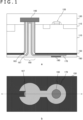
- FIG. 1 depicts diagrams illustrating an example of a structure of a semiconductor apparatus in a first embodiment of the present technology.
- a illustrates a sectional view
- b illustrates a back view.
- a via (TSV) 160 that vertically penetrates a silicon (Si) substrate 110 is provided.
- the silicon substrate 110 is an example of a given layer recited in claims.
- a transistor 120 is formed on the silicon substrate 110. Elements on the silicon substrate 110 are isolated by STI (Shallow Trench Isolation) 115.
- An interlayer insulating film 130 is formed on an upper surface side of the silicon substrate 110.
- Wiring 140 is formed in the interlayer insulating film 130.
- the wiring 140 includes, for example, aluminum (Al) or copper (Cu) as a material. It should be noted that the wiring 140 is an example of an upper surface side material of a layer recited in the claims.
- An insulating film 150 is formed on a lower surface side of the silicon substrate 110.
- the via 160 that penetrates the silicon substrate 110 from the insulating film 150 and stretches to a front of the wiring 140 is formed.
- a side wall 163 is formed inside the via 160.
- An insulating material is used for the side wall 163 to ensure electrical insulation from the silicon substrate 110. It should be noted that the side wall 163 is an example of a side wall recited in the claims.
- the wiring 170 is formed further inside the via 160.
- the wiring 170 is formed in a manner of being pulled out to an outside of the insulating film 150.
- the wiring 170 includes, for example, aluminum or copper as a material. Although the material inside the via 160 and the material outside the insulating film 150 are combined and formed as the wiring 170 in this example, these may be formed as different materials. That is, the wiring 170 is an example of a lower surface side material of a layer and a conductor recited in the claims.
- a cavity portion 167 is formed between the wiring 170 and the side wall 163.
- the cavity portion 167 is formed by etching as will be described later. Accordingly, the wiring 170 outside the insulating film 150 includes an opening portion for supplying the etchant as illustrated in b of FIG. 1 .
- An insulating layer 180 is formed under the wiring 170.
- the insulating layer 180 is also formed inside the wiring 170 of the via 160.
- an opening is provided at a position corresponding to that of the wiring 170, and a bump 190 is formed in the opening.
- the bump 190 is a pad that includes, for example, copper (Cu) as a material. It should be noted that the insulating layer 180 is not illustrated in the back view.
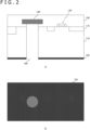
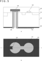
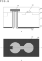
- FIGS. 2 to 6 are diagrams illustrating examples of procedures of a semiconductor apparatus manufacturing method in the first embodiment of the present technology.
- a illustrates sectional views
- b illustrates back views.
- the transistor 120 is formed on the silicon substrate 110. Further, the interlayer insulating film 130 is formed on the upper surface side of the silicon substrate 110. The wiring 140 is formed in the interlayer insulating film 130 (BEOL: Back End Of Line).
- the insulating film 150 is formed on the lower surface side of the silicon substrate 110. Further, an opening of the via 160 is formed in a region that vertically penetrates the silicon substrate 110 from the insulating film 150 and stretches to the front of the wiring 140.
- the side wall 163 is formed inside the via 160.
- the side wall 163 is formed by CVD (Chemical Vapor Deposition) and etchback.
- a side wall 165 is formed further inside the side wall 163.
- the side wall 165 is also formed by CVD and etchback as with the side wall 163. It should be noted, however, that a material having a higher etching rate than those of the side wall 163 and the insulating film 150 are used for this CVD film. Specifically, a BSG (Boron Silica Glass)- or BPSG (Boron Phosphorus Silica Glass)-based film or a resin-based material is used. It should be noted that the side wall 165 is an example of an etching target material recited in the claims.
- a resin-based material for the side wall 165
- a material that includes a base resin having carboxylic acid, an inorganic filler, epoxy resin, and a pigment may be used.
- cyclized polyisoprene or cyclized polybutadiene obtained by cyclizing polyisoprene or polybutadiene may be used for the base resin.
- a novolac resin and a 1,2-naphthoquinonediazide sulfonic acid ester-based compound may be used.
- polycinnamic acid vinyl epoxy resin
- polysiloxane polyamideimide
- polyoxazole polyacrylamide
- cresol novolac polyisoprene
- polyvinyl alcohol and the like may also each be used.
- examples of resin solvents that can be used are diethylene glycol monoethyl ether acetate, diethylene glycol monobutyl ether acetate, diethylene glycol monoethyl ether acetate, diethylene glycol monobutyl ether acetate, tetramethylammonium hydroxide, tetramethylammonium hydroxide, tetrabutylammonium hydroxide, and the like.
- ashing by oxygen plasma, ashing by ozone, and the like are possible as resin etching methods other than solvents.
- the wiring 170 is formed further inside the side wall 165.
- the wiring 170 is formed in a manner of being pulled out to an outside of the insulating film 150. That is, the wiring 170 inside the side wall 165 is maintained in contact with the wiring 170 outside the insulating film 150 and the wiring 140 of the interlayer insulating film 130. Also, an opening portion is provided in the wiring 170 outside the insulating film 150, and part of the side wall 165 is exposed.
- the side wall 165 is removed by photolithography and wet etching, forming the cavity portion 167 between the wiring 170 and the side wall 163.
- the etchant used for wet etching is supplied from the opening portion of the wiring 170 outside the insulating film 150.
- the insulating layer 180 is formed under the wiring 170, an opening is provided at the position corresponding to that of the wiring 170, and the bump 190 is formed in that opening. This forms the above semiconductor apparatus structure.
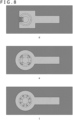
- FIGS. 7 to 9 are diagrams illustrating an example of a shape of the wiring 170 outside the insulating film 150 of the semiconductor apparatus in the first embodiment of the present technology.
- a is an example of a shape similar to that of the above first embodiment, in which an opening portion is formed by a rectangular notch being added in a circular shape.
- b is an example of a shape in which an opening portion is formed by a fan-shaped notch being added in a circular shape.
- c is an example of a shape in which an opening portion is partially formed in a circular shape.
- a contact area between the wiring 170 and the insulating film 150 increases as compared to the above examples, reinforcing strength for fastening the wiring 170.
- d is an example of a shape in which an opening portion is formed by a rectangular notch being added in a rectangular shape.
- e and f are examples of shapes in which multiple opening portions are formed in a circular shape. In this case, as the number of opening portions increases, it becomes easier to perform etching for forming the cavity portion 167.
- g is an example of a shape in which an etching hole is formed in a circular shape.
- h is an example of a shape in which multiple etching holes are formed in a circular shape.
- i is an example of a shape in which multiple etching holes are formed in a rectangular shape. In this case, as the number of etching holes increases, it becomes easier to perform etching for forming the cavity portion 167.
- 1 is an example of a shape in which multiple rectangular etching openings are formed in a circular shape. In this case, etching becomes easier than in the example of h even in the case of misalignment.
- the cavity portion 167 that vertically penetrates the silicon substrate 110 around the wiring 170 inside the via 160 is formed by removal of, by etching, the side wall 165 that includes a material having a high wet etching rate. This decreases a dielectric constant of a side surface of the via 160 and reduces parasitic capacitance, enabling high-speed operation of the semiconductor apparatus.
- an element arrangement prohibition region referred to as a KOZ Keep-Out-Zone
- a KOZ Keep-Out-Zone
- the use of the cavity portion 167 as a TSV side surface film reduces transfer of TSV stress, thereby reducing the KOZ and allowing downsizing of a chip.
- FIG. 10 is a diagram illustrating an example of a structure of a semiconductor apparatus in a second embodiment of the present technology.
- the semiconductor apparatus in this second embodiment is included in an imaging apparatus having a stacked structure.
- This imaging apparatus includes a CIS (CMOS Image Sensor) layer, a logic circuit layer, and a back surface wiring and extraction electrode layer.
- CIS CMOS Image Sensor
- an opening of a via 760 that vertically penetrates a silicon substrate 710 from an insulating film 750 and stretches to the front of wiring 740 is formed in the back surface wiring and extraction electrode layer. Further, a cavity portion 767 is formed between a side wall 763 of the via 760 and wiring 770. An insulating layer 780 is formed under the wiring 770, an opening is provided at the position corresponding to that of the wiring 770, and a bump 790 is formed in the opening. It should be noted that the silicon substrate 710 is an example of a given layer recited in the claims.
- the wiring 740 is formed in an insulating film 703 of the logic circuit.
- the wiring 740 is further connected to other wiring and connects to a bump 713 on an upper surface of the logic circuit.
- the bump 713 on the upper surface of the logic circuit is electrically connected to a bump 712 on a lower surface of the CIS (e.g., Cu-Cu connection).
- the bump 712 on the lower surface of the CIS is further connected to wiring formed in an insulating film 702 of the CIS.
- the CIS includes not only color filters 730 on an upper surface of a silicon substrate 711 but also pixel transistors 721 on a lower surface thereof.
- the structure of the back surface wiring and extraction electrode layer in this second embodiment is similar to that of the above first embodiment. Moreover, the manufacturing method thereof is similar to that of the first embodiment, and a detailed description will be omitted.
- the second embodiment of the present technology it is possible to reduce parasitic capacitance and enable high-speed operation of the imaging apparatus by forming, on the back surface of the CMOS image sensor, the cavity portion 767 that vertically penetrates the silicon substrate 710 around the wiring 770 inside the via 760.
- FIG. 11 is a diagram illustrating an example of a structure of a semiconductor apparatus in the third embodiment of the present technology.
- an opening of a via 260 that vertically penetrates a silicon substrate 210 from an insulating film 250 and stretches to the front of wiring 240 of the logic circuit is formed in the imaging apparatus having a stacked structure. Further, a cavity portion 267 is formed between a side wall 263 of the via 260 and wiring 270. An insulating layer 280 is formed on top of the wiring 270, and an opening for providing a pad is provided at the position corresponding to that of the wiring 270. It should be noted that the silicon substrate 210 is an example of the given layer recited in the claims.
- the wiring 240 is connected to other wiring of the logic circuit and connects to a bump on an upper surface of the logic circuit.
- the bump on the upper surface of the logic circuit is electrically connected to the bump on the lower surface of the CIS.
- the CIS includes not only color filters 230 on the upper surface of the silicon substrate 210 but also pixel transistors 221 on the lower surface thereof.
- FIGS. 12 to 16 are diagrams illustrating an example of a procedure of a semiconductor apparatus manufacturing method in the third embodiment of the present technology.
- a illustrates sectional views
- b illustrates top views.
- an interlayer insulating film 202 of the CIS is stacked on an interlayer insulating film 203 of the logic circuit, and the silicon substrate 210 is stacked further thereon.
- the wiring 240 is formed in the interlayer insulating film 203.
- the wiring 240 includes, for example, aluminum as a material.
- the insulating film 250 is formed by CVD on the upper surface of the silicon substrate 210. Then, the via 260 is formed by an opening being formed in the region that vertically penetrates the silicon substrate 210 from the insulating film 250 and stretches to the front of wiring 240 of the logic circuit.
- an insulating film is further formed from the upper surface by CVD. Thereafter, this insulating film is etched back, forming the side wall 263.
- resin 265 is applied and cured by light irradiation. Thereafter, the resin 265 is etched back as illustrated in FIG. 14 .
- the wiring 270 is formed.
- aluminum is used as a material, and a thin film is formed by sputtering. Then, the film is patterned by photoresist, and the resist is removed by dry etching.
- the wiring 270 inside the resin 265 is maintained in contact with the wiring 270 outside the insulating film 250 and the wiring 240 of the interlayer insulating film 203. Further, an opening portion is provided in the wiring 270 outside the insulating film 250, and part of the resin 265 is exposed.
- the resin 265 is removed by photolithography and wet etching, forming the cavity portion 267 between the wiring 270 and the side wall 263.
- the etchant used for wet etching is supplied from the opening portion of the wiring 270 outside the insulating film 250.
- the insulating layer 280 is formed on top of the wiring 270 by CVD, and an opening for providing a pad is formed at the position corresponding to that of the wiring 270. This forms the above semiconductor apparatus structure.
- the third embodiment of the present technology it is possible to reduce parasitic capacitance and enable high-speed operation of the imaging apparatus by forming, on the front surface of the CMOS image sensor, the cavity portion 267 that vertically penetrates the silicon substrate 210 around the wiring 270 inside the via 260.
- FIG. 17 depicts diagrams illustrating an example of a structure of a semiconductor apparatus in a fourth embodiment of the present technology.
- a illustrates a sectional view
- b illustrates a top view.
- a cavity portion 367 is formed around wiring 370 inside the TSV that vertically penetrates the interlayer insulating films 310 to 312. That is, parasitic capacitance is reduced by the cavity portion 367 being provided in the interlayer insulating films 310 to 312 instead of in the silicon substrate 110 or the like as in the above embodiments.
- the interlayer insulating films 310 to 312 are examples of the given layer recited in the claims. Also, a description will be given of this example by assuming that copper is used as the material of the wiring 370.
- FIGS. 18 to 23 are diagrams illustrating an example of a procedure of a semiconductor apparatus manufacturing method in the fourth embodiment of the present technology.
- a illustrates sectional views
- b illustrates top views.
- wiring 340 is formed.
- the wiring 340 includes, for example, copper as a material.
- the interlayer insulating film 310 is formed in such a manner as to include the wiring 340.
- a wiring trench 361 for forming new wiring is formed by resist patterning.
- a via 360 is formed by resist patterning, etching, and resist removal.
- resin 365 is applied and cured by light irradiation. Thereafter, the resin 365 is etched back as illustrated in FIG. 20 .
- the wiring 370 inside the via 360 is maintained in contact with the wiring 370 of the wiring trench 361 and the wiring 340. Also, the wiring 370 of the wiring trench 361 has a width smaller than a diameter of the via 360, thus forming an opening portion and exposing part of the resin 365.
- the resin 365 is removed by etching using a solvent, forming the cavity portion 367 around the wiring 370 inside the via 360.
- the solvent used for etching is supplied from the opening portion beside the wiring 370 of the interlayer insulating film 310.
- interlayer insulating films 311 and 312 are sequentially formed on the interlayer insulating film 310.
- wiring is also similarly formed in the interlayer insulating films 311 and 312. That is, a structure including a via and wiring having the cavity portion 367 is also similarly formed for multi-layer wiring by repeating the abovementioned process.
- the fourth embodiment of the present technology it is possible to reduce parasitic capacitance and enable high-speed operation of the imaging apparatus by forming, around the wiring 370 of the via 360, the cavity portion 367 in the damascene process.
- FIG. 24 depicts diagrams illustrating an example of a structure of a semiconductor apparatus in a fifth embodiment of the present technology.
- a illustrates a sectional view
- b illustrates a top view.
- a cavity portion 467 is formed around wiring 471 inside a via between wiring 440 and wiring 472. That is, parasitic capacitance is reduced by the cavity portion 467 being provided in an interlayer insulating film 410.
- the interlayer insulating film 410 is an example of the given layer recited in the claims.
- FIGS. 25 to 29 are diagrams illustrating an example of a procedure of a semiconductor apparatus manufacturing method in the fifth embodiment of the present technology.
- a illustrates sectional views
- b illustrates top views.
- the wiring 440 is formed.
- the wiring 440 includes, for example, aluminum or copper as a material.
- the interlayer insulating film 410 is formed in such a manner as to include the wiring 440.
- a via 460 is formed by resist patterning, etching, and resist removal.
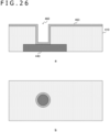
- resin 463 is applied and cured by light irradiation. Thereafter, the resin 463 is etched back as illustrated in FIG. 27 .
- tungsten (W) or the like is embedded into the via 460, and CMP is performed. This forms the wiring 471.
- the via 460 is formed by resist patterning, metal etching, and resist removal.
- the wiring 472 is formed.
- the wiring 472 inside the via 460 is maintained in contact with the wiring 470 and the wiring 440. Also, the wiring 472 has the width smaller than the diameter of the via 460, thus forming an opening portion and exposing part of the resin 463.
- the resin 463 is removed by etching using a solvent, forming the cavity portion 467 around the wiring 471 inside the via 460.
- the solvent used for etching is supplied from the opening portion beside the wiring 472 of the interlayer insulating film 410.
- an interlayer insulating film 411 is formed on top of the wiring 472 by CVD. This forms the above semiconductor apparatus structure.
- the fifth embodiment of the present technology it is possible to reduce parasitic capacitance and enable high-speed operation of the imaging apparatus by forming the cavity portion 467 around the wiring 471 inside the via 460 of the interlayer insulating film 410.
- a vertically penetrating cavity portion is provided inside the TSV
- such a cavity portion may be provided outside the TSV. It should be noted that although a description will be given of an example in which a cavity portion is provided only outside the TSV in the following embodiments, a cavity portion may also be provided inside the TSV in combination with the above embodiments.
- FIG. 30 depicts diagrams illustrating an example of a structure of a semiconductor apparatus in a sixth embodiment of the present technology.
- a illustrates a sectional view
- b illustrates a back view.
- a vertically penetrating via 561 is formed in a ring shape around the TSV which is a center.
- the via 561 includes a cavity portion 568 in a region sandwiched between upside wiring 541 and a downside insulating layer 580. It is possible to reduce parasitic capacitance in the TSV by providing the cavity portion 568. It should be noted that the via 561 is an example of a surrounding trench recited in the claims.
- FIGS. 31 to 35 are diagrams illustrating an example of a procedure of a semiconductor apparatus manufacturing method in the sixth embodiment of the present technology.
- a illustrates sectional views
- b illustrates back views.
- a transistor 520 is formed on a silicon substrate 510. Also, an interlayer insulating film 530 is formed on the upper surface side of the silicon substrate 510. Wiring 540 and wiring 541 are formed in the interlayer insulating film 530. The wiring 540 and the wiring 541 include, for example, copper as a material. It should be noted that the silicon substrate 510 is an example of the given layer recited in the claims.
- an insulating film 550 is formed on the lower surface side of the silicon substrate 510. Further, an opening of the via 561 is formed in a region that vertically penetrates in a ring shape the silicon substrate 510 from the insulating film 550 and stretches to the front of the wiring 541.
- an insulating film 569 is formed on the lower surface side of the insulating film 550.
- CVD is used to form the insulating film 569
- CVD in this case is performed in a poor step coverage condition. This ensures that while the insulating film 569 is formed in a downside of the via 561, the insulating film 569 is not formed in an interior (upside) of the via 561, making it possible to secure the cavity portion 568.
- the insulating film 569 under the insulating film 550 is shaved by CMP, leaving the insulating film 569 unshaved inside the via 561.
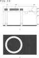
- photoresist 581 for forming an opening in the TSV is patterned, and a via 560 is formed by etching. Thereafter, the photoresist 581 is removed.
- a side wall 563 is formed inside the via 560.
- the side wall 563 is formed by CVD and etchback of an insulating film.
- wiring 570 is formed inside the side wall 563.
- the wiring 570 is formed in a manner of being pulled out to an outside of the insulating film 550.
- the wiring 570 includes, for example, copper as a material.
- an insulating layer 580 is formed under the wiring 570, an opening is provided at a position corresponding to that of the wiring 570, and a bump 590 is formed in the opening. This forms the above semiconductor apparatus structure.
- the sixth embodiment of the present technology it is possible to reduce parasitic capacitance and enable high-speed operation of the imaging apparatus by providing the vertically penetrating via 561 in a ring-shape outside the inside of the via 560 of the silicon substrate 510 and forming the cavity portion 568 in the via 561.
- FIG. 36 depicts diagrams illustrating an example of a structure of a semiconductor apparatus in a seventh embodiment of the present technology.
- a illustrates a sectional view
- b illustrates a back view.
- a silicide 641 is provided on the silicon substrate 610 to stop the etching at the silicide 641 in this seventh embodiment.
- the silicide 641 includes, for example, TiSi, CoSi, or the like as a material.
- copper wiring is not used as an etch stop unlike in the above sixth embodiment, making it possible to improve a degree of freedom in wiring layout.
- processing steps described in the above embodiments may be regarded as a method having a series of these steps, a program for causing a computer to perform the series of these steps, or a recording medium storing the program.
- a CD Compact Disc
- MD MiniDisc
- DVD Digital Versatile Disc
- a memory card a Blu-ray (registered trademark) Disc, or the like can be used as this recording medium.
Landscapes
- Internal Circuitry In Semiconductor Integrated Circuit Devices (AREA)
- Solid State Image Pick-Up Elements (AREA)
Abstract
Description
- The present technology relates to a semiconductor apparatus. More specifically, the present technology relates to a semiconductor apparatus having a through electrode and a manufacturing method of the same.
- There is known a through-silicon via (TSV) technology that extracts electrodes from a back side of a semiconductor substrate as a semiconductor apparatus downsizing technology. In this TSV, increase in speed may be hindered by presence of parasitic capacitance with a semiconductor substrate on a side surface of the TSV that penetrates the semiconductor substrate. Meanwhile, a device having an isolation recess portion formed in a TSV's liner isolation layer has been proposed for the purpose of mitigating the impact caused by the stress of the TSV (refer, for example, to PTL 1).
- [PTL1]
Japanese Translations of PCT for Patent No. 2015-511765 - In the above technology of the related art, an air gap is partially formed by an isolation recess portion being provided. However, this isolation recess portion is provided to mitigate the impact of stress caused by the TSV and is not sufficient to reduce parasitic capacitance.
- The present technology has been devised in light of the foregoing, and it is an object thereof to reduce the parasitic capacitance in the TSV.
- The present technology has been devised to solve the above problem, and a first aspect thereof is a semiconductor apparatus that includes a via that vertically penetrates a given layer, an upper surface side material and a lower surface side material of the layer, and a conductor that is in contact with the upper surface side material and the lower surface side material of the layer and that forms, between the conductor and an inside of the via, a cavity portion that vertically penetrates the layer. This has an action of forming the cavity portion around the conductor and reducing parasitic capacitance.
- Also, in this first aspect, at least either the upper surface side material or the lower surface side material of the layer may be a conductive material, and at least part of the conductive material may include an opening portion for the cavity portion. This has an action of supplying an etchant from the opening portion when the cavity portion is formed.
- Further, in this first aspect, the layer may be a semiconductor substrate or an insulating film.
- Further, in this first aspect, an insulating side wall formed inside the via may also be included. This has an action of ensuring electrical insulation even in a case where the layer is a semiconductor substrate.
- Further, in this first aspect, the conductor may include an insulating material thereinside.
- Further, in this first aspect, the conductor may form wiring.
- Further, in this first aspect, a surrounding trench that vertically penetrates the layer at a circumference of the via may further be included.
- Further, a second aspect of the present technology is an imaging apparatus having a stacked structure that includes multiple layers, and the imaging apparatus includes a via that vertically penetrates a given layer of the multiple layers, an upper surface side material and a lower surface side material of the layer, and a conductor that is in contact with the upper surface side material and the lower surface side material of the layer and that forms, between the conductor and an inside of the via, a cavity portion that vertically penetrates the layer. This has an action of forming the cavity portion around the conductor and reducing parasitic capacitance.
- Further, in this second aspect, at least either the upper surface side material or the lower surface side material of the layer may be a conductive material, and at least part of the conductive material may include an opening portion for the cavity portion. This has an action of supplying an etchant from the opening portion when the cavity portion is formed.
- Further, in this second aspect, the conductive material may be arranged on a surface opposed to an incident light side or on the same surface as the incident light side.
- Further, a third aspect of the present technology is a semiconductor apparatus manufacturing method that includes a step of forming a via that vertically penetrates a given layer, a step of forming, inside the via, an etching target material having an etching rate different from that of the layer, a step of forming a conductor inside the etching target material, and a step of etching the etching target material with the conductor in contact with an upper surface side material and a lower surface side material of the layer. This has an action of forming the cavity portion around the conductor by etching, and reducing parasitic capacitance.
- Further, in this third aspect, at least either the upper surface side material or the lower surface side material of the layer may be a conductive material, and a step of shaping the conductive material such that the etching target material is exposed at least at part of the conductive material may further be included. This has an action of forming a cavity portion by etching the exposed etching target material.
-
- [
FIG. 1 ]
FIG. 1 depicts diagrams illustrating an example of a structure of a semiconductor apparatus in a first embodiment of the present technology. - [
FIG. 2 ]
FIG. 2 depicts first diagrams illustrating an example of a procedure of a semiconductor apparatus manufacturing method in the first embodiment of the present technology. - [
FIG. 3 ]
FIG. 3 depicts second diagrams illustrating an example of a procedure of the semiconductor apparatus manufacturing method in the first embodiment of the present technology. - [
FIG. 4 ]
FIG. 4 depicts third diagrams illustrating an example of a procedure of the semiconductor apparatus manufacturing method in the first embodiment of the present technology. - [
FIG. 5 ]
FIG. 5 depicts fourth diagrams illustrating an example of a procedure of the semiconductor apparatus manufacturing method in the first embodiment of the present technology. - [
FIG. 6 ]
FIG. 6 depicts fifth diagrams illustrating an example of a procedure of the semiconductor apparatus manufacturing method in the first embodiment of the present technology. - [
FIG. 7 ]
FIG. 7 depicts first diagrams illustrating an example of a shape of wiring 170 outside aninsulating film 150 of the semiconductor apparatus in the first embodiment of the present technology. - [
FIG. 8 ]
FIG. 8 depicts second diagrams illustrating an example of a shape of thewiring 170 outside theinsulating film 150 of the semiconductor apparatus in the first embodiment of the present technology. - [
FIG. 9 ]
FIG. 9 depicts second diagrams illustrating an example of a shape of thewiring 170 outside theinsulating film 150 of the semiconductor apparatus in the first embodiment of the present technology. - [
FIG. 10 ]
FIG. 10 is a diagram illustrating an example of a structure of a semiconductor apparatus in a second embodiment of the present technology. - [
FIG. 11 ]
FIG. 11 is a diagram illustrating an example of a structure of a semiconductor apparatus in a third embodiment of the present technology. - [
FIG. 12 ]
FIG. 12 depicts first diagrams illustrating an example of a procedure of a semiconductor apparatus manufacturing method in the third embodiment of the present technology. - [
FIG. 13 ]
FIG. 13 depicts second diagrams illustrating an example of a procedure of the semiconductor apparatus manufacturing method in the third embodiment of the present technology. - [
FIG. 14 ]
FIG. 14 depicts third diagrams illustrating an example of a procedure of the semiconductor apparatus manufacturing method in the third embodiment of the present technology. - [
FIG. 15 ]
FIG. 15 depicts fourth diagrams illustrating an example of a procedure of the semiconductor apparatus manufacturing method in the third embodiment of the present technology. - [
FIG. 16 ]
FIG. 16 depicts fifth diagrams illustrating an example of a procedure of the semiconductor apparatus manufacturing method in the third embodiment of the present technology. - [
FIG. 17 ]
FIG. 17 depicts diagrams illustrating an example of a structure of a semiconductor apparatus in a fourth embodiment of the present technology. - [
FIG. 18 ]
FIG. 18 depicts first diagrams illustrating an example of a procedure of a semiconductor apparatus manufacturing method in the fourth embodiment of the present technology. - [
FIG. 19 ]
FIG. 19 depicts second diagrams illustrating an example of a procedure of the semiconductor apparatus manufacturing method in the fourth embodiment of the present technology. - [
FIG. 20 ]
FIG. 20 depicts third diagrams illustrating an example of a procedure of the semiconductor apparatus manufacturing method in the fourth embodiment of the present technology. - [
FIG. 21 ]
FIG. 21 depicts fourth diagrams illustrating an example of a procedure of the semiconductor apparatus manufacturing method in the fourth embodiment of the present technology. - [
FIG. 22 ]
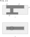
FIG. 22 depicts fifth diagrams illustrating an example of a procedure of the semiconductor apparatus manufacturing method in the fourth embodiment of the present technology. - [
FIG. 23 ]
FIG. 23 depicts sixth diagrams illustrating an example of a procedure of the semiconductor apparatus manufacturing method in the fourth embodiment of the present technology. - [
FIG. 24 ]
FIG. 24 depicts diagrams illustrating an example of a structure of a semiconductor apparatus in a fifth embodiment of the present technology. - [
FIG. 25 ]
FIG. 25 depicts first diagrams illustrating an example of a procedure of a semiconductor apparatus manufacturing method in the fifth embodiment of the present technology. - [
FIG. 26 ]
FIG. 26 depicts second diagrams illustrating an example of a procedure of the semiconductor apparatus manufacturing method in the fifth embodiment of the present technology. - [
FIG. 27 ]
FIG. 27 depicts third diagrams illustrating an example of a procedure of the semiconductor apparatus manufacturing method in the fifth embodiment of the present technology. - [
FIG. 28 ]
FIG. 28 depicts fourth diagrams illustrating an example of a procedure of the semiconductor apparatus manufacturing method in the fifth embodiment of the present technology. - [
FIG. 29 ]
FIG. 29 depicts fifth diagrams illustrating an example of a procedure of the semiconductor apparatus manufacturing method in the fifth embodiment of the present technology. - [
FIG. 30 ]
FIG. 30 depicts diagrams illustrating an example of a structure of a semiconductor apparatus in a sixth embodiment of the present technology. - [
FIG. 31 ]
FIG. 31 depicts first diagrams illustrating an example of a procedure of the semiconductor apparatus manufacturing method in the sixth embodiment of the present technology. - [
FIG. 32 ]
FIG. 32 depicts second diagrams illustrating an example of a procedure of the semiconductor apparatus manufacturing method in the sixth embodiment of the present technology. - [
FIG. 33 ]
FIG. 33 depicts third diagrams illustrating an example of a procedure of the semiconductor apparatus manufacturing method in the sixth embodiment of the present technology. - [
FIG. 34 ]
FIG. 34 depicts fourth diagrams illustrating an example of a procedure of the semiconductor apparatus manufacturing method in the sixth embodiment of the present technology. - [
FIG. 35 ]
FIG. 35 depicts fifth diagrams illustrating an example of a procedure of the semiconductor apparatus manufacturing method in the sixth embodiment of the present technology. - [
FIG. 36 ]
FIG. 36 depicts diagrams illustrating an example of a structure of a semiconductor apparatus in a seventh embodiment of the present technology. - A description will be given below of modes for carrying out the present technology (hereinafter referred to as embodiments). The description will be given in the following order.
- 1. First embodiment (example of application to an opening on a wafer back surface)
- 2. Second embodiment (example of application to a stacked CIS back surface)
- 3. Third embodiment (example of application to a stacked CIS front surface)
- 4. Fourth embodiment (example of application to a wiring formation process)
- 5. Fifth embodiment (example of application to a via)
- 6. Sixth embodiment (first example of application to a surrounding portion)
- 7. Seventh embodiment (second example of application to a surrounding portion)
-
FIG. 1 depicts diagrams illustrating an example of a structure of a semiconductor apparatus in a first embodiment of the present technology. InFIG. 1 , a illustrates a sectional view, and b illustrates a back view. - In this semiconductor apparatus, a via (TSV) 160 that vertically penetrates a silicon (Si)
substrate 110 is provided. It should be noted that thesilicon substrate 110 is an example of a given layer recited in claims. - A
transistor 120 is formed on thesilicon substrate 110. Elements on thesilicon substrate 110 are isolated by STI (Shallow Trench Isolation) 115. - An interlayer insulating
film 130 is formed on an upper surface side of thesilicon substrate 110. Wiring 140 is formed in theinterlayer insulating film 130. Thewiring 140 includes, for example, aluminum (Al) or copper (Cu) as a material. It should be noted that thewiring 140 is an example of an upper surface side material of a layer recited in the claims. - An insulating
film 150 is formed on a lower surface side of thesilicon substrate 110. The via 160 that penetrates thesilicon substrate 110 from the insulatingfilm 150 and stretches to a front of thewiring 140 is formed. - A
side wall 163 is formed inside the via 160. An insulating material is used for theside wall 163 to ensure electrical insulation from thesilicon substrate 110. It should be noted that theside wall 163 is an example of a side wall recited in the claims. - The
wiring 170 is formed further inside the via 160. Thewiring 170 is formed in a manner of being pulled out to an outside of the insulatingfilm 150. Thewiring 170 includes, for example, aluminum or copper as a material. Although the material inside the via 160 and the material outside the insulatingfilm 150 are combined and formed as thewiring 170 in this example, these may be formed as different materials. That is, thewiring 170 is an example of a lower surface side material of a layer and a conductor recited in the claims. - A
cavity portion 167 is formed between thewiring 170 and theside wall 163. Thecavity portion 167 is formed by etching as will be described later. Accordingly, thewiring 170 outside the insulatingfilm 150 includes an opening portion for supplying the etchant as illustrated in b ofFIG. 1 . - An insulating
layer 180 is formed under thewiring 170. The insulatinglayer 180 is also formed inside thewiring 170 of thevia 160. In the insulatinglayer 180, an opening is provided at a position corresponding to that of thewiring 170, and abump 190 is formed in the opening. Thebump 190 is a pad that includes, for example, copper (Cu) as a material. It should be noted that the insulatinglayer 180 is not illustrated in the back view. -
FIGS. 2 to 6 are diagrams illustrating examples of procedures of a semiconductor apparatus manufacturing method in the first embodiment of the present technology. In respectiveFIGS. 2 to 6 , a illustrates sectional views, and b illustrates back views. - First, as illustrated in
FIG. 2 , thetransistor 120 is formed on thesilicon substrate 110. Further, theinterlayer insulating film 130 is formed on the upper surface side of thesilicon substrate 110. Thewiring 140 is formed in the interlayer insulating film 130 (BEOL: Back End Of Line). - Further, the insulating
film 150 is formed on the lower surface side of thesilicon substrate 110. Further, an opening of thevia 160 is formed in a region that vertically penetrates thesilicon substrate 110 from the insulatingfilm 150 and stretches to the front of thewiring 140. - Next, as illustrated in
FIG. 3 , theside wall 163 is formed inside the via 160. Theside wall 163 is formed by CVD (Chemical Vapor Deposition) and etchback. - Then, as illustrated in
FIG. 4 , aside wall 165 is formed further inside theside wall 163. Theside wall 165 is also formed by CVD and etchback as with theside wall 163. It should be noted, however, that a material having a higher etching rate than those of theside wall 163 and the insulatingfilm 150 are used for this CVD film. Specifically, a BSG (Boron Silica Glass)- or BPSG (Boron Phosphorus Silica Glass)-based film or a resin-based material is used. It should be noted that theside wall 165 is an example of an etching target material recited in the claims. - In a case where a resin-based material is used for the
side wall 165, for example, a material that includes a base resin having carboxylic acid, an inorganic filler, epoxy resin, and a pigment may be used. Also, cyclized polyisoprene or cyclized polybutadiene obtained by cyclizing polyisoprene or polybutadiene may be used for the base resin. Moreover, a novolac resin and a 1,2-naphthoquinonediazide sulfonic acid ester-based compound may be used. In addition, polycinnamic acid vinyl, epoxy resin, polysiloxane, polyamideimide, polyoxazole, polyacrylamide, cresol novolac, polyisoprene, polyvinyl alcohol, and the like may also each be used. - In this case, examples of resin solvents that can be used are diethylene glycol monoethyl ether acetate, diethylene glycol monobutyl ether acetate, diethylene glycol monoethyl ether acetate, diethylene glycol monobutyl ether acetate, tetramethylammonium hydroxide, tetramethylammonium hydroxide, tetrabutylammonium hydroxide, and the like. Also, ashing by oxygen plasma, ashing by ozone, and the like are possible as resin etching methods other than solvents.
- Next, as illustrated in
FIG. 5 , thewiring 170 is formed further inside theside wall 165. Thewiring 170 is formed in a manner of being pulled out to an outside of the insulatingfilm 150. That is, thewiring 170 inside theside wall 165 is maintained in contact with thewiring 170 outside the insulatingfilm 150 and thewiring 140 of theinterlayer insulating film 130. Also, an opening portion is provided in thewiring 170 outside the insulatingfilm 150, and part of theside wall 165 is exposed. - Further, in this state, as illustrated in
FIG. 6 , theside wall 165 is removed by photolithography and wet etching, forming thecavity portion 167 between thewiring 170 and theside wall 163. At this time, the etchant used for wet etching is supplied from the opening portion of thewiring 170 outside the insulatingfilm 150. - Thereafter, the insulating
layer 180 is formed under thewiring 170, an opening is provided at the position corresponding to that of thewiring 170, and thebump 190 is formed in that opening. This forms the above semiconductor apparatus structure. -
FIGS. 7 to 9 are diagrams illustrating an example of a shape of thewiring 170 outside the insulatingfilm 150 of the semiconductor apparatus in the first embodiment of the present technology. - In
FIG. 7 , a is an example of a shape similar to that of the above first embodiment, in which an opening portion is formed by a rectangular notch being added in a circular shape. - In
FIG. 7 , b is an example of a shape in which an opening portion is formed by a fan-shaped notch being added in a circular shape. - In
FIG. 7 , c is an example of a shape in which an opening portion is partially formed in a circular shape. In this case, a contact area between thewiring 170 and the insulatingfilm 150 increases as compared to the above examples, reinforcing strength for fastening thewiring 170. - In
FIG. 8 , d is an example of a shape in which an opening portion is formed by a rectangular notch being added in a rectangular shape. - In
FIG. 8 , e and f are examples of shapes in which multiple opening portions are formed in a circular shape. In this case, as the number of opening portions increases, it becomes easier to perform etching for forming thecavity portion 167. - In
FIG. 9 , g is an example of a shape in which an etching hole is formed in a circular shape. - In
FIG. 9 , h is an example of a shape in which multiple etching holes are formed in a circular shape. InFIG. 9 , i is an example of a shape in which multiple etching holes are formed in a rectangular shape. In this case, as the number of etching holes increases, it becomes easier to perform etching for forming thecavity portion 167. - In
FIG. 9 ,1 is an example of a shape in which multiple rectangular etching openings are formed in a circular shape. In this case, etching becomes easier than in the example of h even in the case of misalignment. - Thus, in the first embodiment of the present technology, the
cavity portion 167 that vertically penetrates thesilicon substrate 110 around thewiring 170 inside the via 160 is formed by removal of, by etching, theside wall 165 that includes a material having a high wet etching rate. This decreases a dielectric constant of a side surface of the via 160 and reduces parasitic capacitance, enabling high-speed operation of the semiconductor apparatus. - Further, in general, an element arrangement prohibition region referred to as a KOZ (Keep-Out-Zone) is provided around the TSV to avoid an impact of stress caused by TSV formation. In this first embodiment, the use of the
cavity portion 167 as a TSV side surface film reduces transfer of TSV stress, thereby reducing the KOZ and allowing downsizing of a chip. -
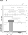
FIG. 10 is a diagram illustrating an example of a structure of a semiconductor apparatus in a second embodiment of the present technology. - The semiconductor apparatus in this second embodiment is included in an imaging apparatus having a stacked structure. This imaging apparatus includes a CIS (CMOS Image Sensor) layer, a logic circuit layer, and a back surface wiring and extraction electrode layer.
- In this second embodiment, an opening of a via 760 that vertically penetrates a
silicon substrate 710 from an insulatingfilm 750 and stretches to the front ofwiring 740 is formed in the back surface wiring and extraction electrode layer. Further, acavity portion 767 is formed between aside wall 763 of the via 760 andwiring 770. An insulatinglayer 780 is formed under thewiring 770, an opening is provided at the position corresponding to that of thewiring 770, and abump 790 is formed in the opening. It should be noted that thesilicon substrate 710 is an example of a given layer recited in the claims. - The
wiring 740 is formed in an insulatingfilm 703 of the logic circuit. Thewiring 740 is further connected to other wiring and connects to abump 713 on an upper surface of the logic circuit. Thebump 713 on the upper surface of the logic circuit is electrically connected to abump 712 on a lower surface of the CIS (e.g., Cu-Cu connection). - The
bump 712 on the lower surface of the CIS is further connected to wiring formed in an insulatingfilm 702 of the CIS. The CIS includes not onlycolor filters 730 on an upper surface of asilicon substrate 711 but alsopixel transistors 721 on a lower surface thereof. - The structure of the back surface wiring and extraction electrode layer in this second embodiment is similar to that of the above first embodiment. Moreover, the manufacturing method thereof is similar to that of the first embodiment, and a detailed description will be omitted.
- As described above, in the second embodiment of the present technology, it is possible to reduce parasitic capacitance and enable high-speed operation of the imaging apparatus by forming, on the back surface of the CMOS image sensor, the
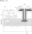
cavity portion 767 that vertically penetrates thesilicon substrate 710 around thewiring 770 inside the via 760. - While an example in which the TSV is provided on the back surface of the CMOS image sensor has been described in the above second embodiment, a description will be given, in this third embodiment, of an example in which the TSV is provided on a front surface of the CMOS image sensor.
-
FIG. 11 is a diagram illustrating an example of a structure of a semiconductor apparatus in the third embodiment of the present technology. - In this third embodiment, an opening of a via 260 that vertically penetrates a
silicon substrate 210 from an insulatingfilm 250 and stretches to the front ofwiring 240 of the logic circuit is formed in the imaging apparatus having a stacked structure. Further, acavity portion 267 is formed between aside wall 263 of the via 260 andwiring 270. An insulatinglayer 280 is formed on top of thewiring 270, and an opening for providing a pad is provided at the position corresponding to that of thewiring 270. It should be noted that thesilicon substrate 210 is an example of the given layer recited in the claims. - The
wiring 240 is connected to other wiring of the logic circuit and connects to a bump on an upper surface of the logic circuit. The bump on the upper surface of the logic circuit is electrically connected to the bump on the lower surface of the CIS. The CIS includes not onlycolor filters 230 on the upper surface of thesilicon substrate 210 but alsopixel transistors 221 on the lower surface thereof. -
FIGS. 12 to 16 are diagrams illustrating an example of a procedure of a semiconductor apparatus manufacturing method in the third embodiment of the present technology. InFIGS. 12 to 16 , a illustrates sectional views, and b illustrates top views. - First, as illustrated in
FIG. 12 , aninterlayer insulating film 202 of the CIS is stacked on aninterlayer insulating film 203 of the logic circuit, and thesilicon substrate 210 is stacked further thereon. Thewiring 240 is formed in theinterlayer insulating film 203. Thewiring 240 includes, for example, aluminum as a material. - The insulating
film 250 is formed by CVD on the upper surface of thesilicon substrate 210. Then, the via 260 is formed by an opening being formed in the region that vertically penetrates thesilicon substrate 210 from the insulatingfilm 250 and stretches to the front ofwiring 240 of the logic circuit. - Then, an insulating film is further formed from the upper surface by CVD. Thereafter, this insulating film is etched back, forming the
side wall 263. - Next, as illustrated in
FIG. 13 ,resin 265 is applied and cured by light irradiation. Thereafter, theresin 265 is etched back as illustrated inFIG. 14 . - Subsequently, as illustrated in
FIG. 15 , thewiring 270 is formed. At this time, it is assumed that aluminum is used as a material, and a thin film is formed by sputtering. Then, the film is patterned by photoresist, and the resist is removed by dry etching. - The
wiring 270 inside theresin 265 is maintained in contact with thewiring 270 outside the insulatingfilm 250 and thewiring 240 of theinterlayer insulating film 203. Further, an opening portion is provided in thewiring 270 outside the insulatingfilm 250, and part of theresin 265 is exposed. - Further, in this state, as illustrated in
FIG. 16 , theresin 265 is removed by photolithography and wet etching, forming thecavity portion 267 between thewiring 270 and theside wall 263. At this time, the etchant used for wet etching is supplied from the opening portion of thewiring 270 outside the insulatingfilm 250. - Thereafter, the insulating
layer 280 is formed on top of thewiring 270 by CVD, and an opening for providing a pad is formed at the position corresponding to that of thewiring 270. This forms the above semiconductor apparatus structure. - As described above, in the third embodiment of the present technology, it is possible to reduce parasitic capacitance and enable high-speed operation of the imaging apparatus by forming, on the front surface of the CMOS image sensor, the
cavity portion 267 that vertically penetrates thesilicon substrate 210 around thewiring 270 inside the via 260. -
FIG. 17 depicts diagrams illustrating an example of a structure of a semiconductor apparatus in a fourth embodiment of the present technology. InFIG. 17 , a illustrates a sectional view, and b illustrates a top view. - In this fourth embodiment, in the structure having
interlayer insulating films 310 to 312 stacked, acavity portion 367 is formed aroundwiring 370 inside the TSV that vertically penetrates the interlayer insulatingfilms 310 to 312. That is, parasitic capacitance is reduced by thecavity portion 367 being provided in theinterlayer insulating films 310 to 312 instead of in thesilicon substrate 110 or the like as in the above embodiments. It should be noted that theinterlayer insulating films 310 to 312 are examples of the given layer recited in the claims. Also, a description will be given of this example by assuming that copper is used as the material of thewiring 370. -
FIGS. 18 to 23 are diagrams illustrating an example of a procedure of a semiconductor apparatus manufacturing method in the fourth embodiment of the present technology. InFIGS. 18 to 23 , a illustrates sectional views, and b illustrates top views. - First, as illustrated in
FIG. 18 ,wiring 340 is formed. Thewiring 340 includes, for example, copper as a material. Next, theinterlayer insulating film 310 is formed in such a manner as to include thewiring 340. Then, in theinterlayer insulating film 310, awiring trench 361 for forming new wiring is formed by resist patterning. - Subsequently, in the
interlayer insulating film 310, a via 360 is formed by resist patterning, etching, and resist removal. - Next, as illustrated in
FIG. 19 ,resin 365 is applied and cured by light irradiation. Thereafter, theresin 365 is etched back as illustrated inFIG. 20 . - Subsequently, as illustrated in
FIG. 21 , copper is plated on the front surfaces of the via 360 and thewiring trench 361, and CMP (Chemical Mechanical Polishing) is performed. This forms thewiring 370. That is, in the fourth embodiment, it is assumed that a damascene process that forms wiring and a via at the same time is used. - At this time, the
wiring 370 inside the via 360 is maintained in contact with thewiring 370 of thewiring trench 361 and thewiring 340. Also, thewiring 370 of thewiring trench 361 has a width smaller than a diameter of the via 360, thus forming an opening portion and exposing part of theresin 365. - Further, in this state, as illustrated in
FIG. 22 , theresin 365 is removed by etching using a solvent, forming thecavity portion 367 around thewiring 370 inside the via 360. At this time, the solvent used for etching is supplied from the opening portion beside thewiring 370 of theinterlayer insulating film 310. - Thereafter, as illustrated in
FIG. 23 ,interlayer insulating films interlayer insulating film 310. Then, wiring is also similarly formed in theinterlayer insulating films cavity portion 367 is also similarly formed for multi-layer wiring by repeating the abovementioned process. - As described above, according to the fourth embodiment of the present technology, it is possible to reduce parasitic capacitance and enable high-speed operation of the imaging apparatus by forming, around the
wiring 370 of the via 360, thecavity portion 367 in the damascene process. -
FIG. 24 depicts diagrams illustrating an example of a structure of a semiconductor apparatus in a fifth embodiment of the present technology. InFIG. 24 , a illustrates a sectional view, and b illustrates a top view. - In this fifth embodiment, a
cavity portion 467 is formed aroundwiring 471 inside a via betweenwiring 440 andwiring 472. That is, parasitic capacitance is reduced by thecavity portion 467 being provided in aninterlayer insulating film 410. It should be noted that theinterlayer insulating film 410 is an example of the given layer recited in the claims. -
FIGS. 25 to 29 are diagrams illustrating an example of a procedure of a semiconductor apparatus manufacturing method in the fifth embodiment of the present technology. InFIGS. 25 to 29 , a illustrates sectional views, and b illustrates top views. - First, as illustrated in
FIG. 25 , thewiring 440 is formed. Thewiring 440 includes, for example, aluminum or copper as a material. Next, theinterlayer insulating film 410 is formed in such a manner as to include thewiring 440. Then, in theinterlayer insulating film 410, a via 460 is formed by resist patterning, etching, and resist removal. - Next, as illustrated in
FIG. 26 ,resin 463 is applied and cured by light irradiation. Thereafter, theresin 463 is etched back as illustrated inFIG. 27 . - Subsequently, as illustrated in
FIG. 28 , tungsten (W) or the like is embedded into the via 460, and CMP is performed. This forms thewiring 471. - Then, the via 460 is formed by resist patterning, metal etching, and resist removal. The
wiring 472 is formed. - At this time, the
wiring 472 inside the via 460 is maintained in contact with the wiring 470 and thewiring 440. Also, thewiring 472 has the width smaller than the diameter of the via 460, thus forming an opening portion and exposing part of theresin 463. - Then, in this state, as illustrated in
FIG. 29 , theresin 463 is removed by etching using a solvent, forming thecavity portion 467 around thewiring 471 inside the via 460. At this time, the solvent used for etching is supplied from the opening portion beside thewiring 472 of theinterlayer insulating film 410. - Thereafter, an
interlayer insulating film 411 is formed on top of thewiring 472 by CVD. This forms the above semiconductor apparatus structure. - As described above, according to the fifth embodiment of the present technology, it is possible to reduce parasitic capacitance and enable high-speed operation of the imaging apparatus by forming the
cavity portion 467 around thewiring 471 inside the via 460 of theinterlayer insulating film 410. - While examples in which a vertically penetrating cavity portion is provided inside the TSV have been described in the above embodiments, such a cavity portion may be provided outside the TSV. It should be noted that although a description will be given of an example in which a cavity portion is provided only outside the TSV in the following embodiments, a cavity portion may also be provided inside the TSV in combination with the above embodiments.
-
FIG. 30 depicts diagrams illustrating an example of a structure of a semiconductor apparatus in a sixth embodiment of the present technology. InFIG. 30 , a illustrates a sectional view, and b illustrates a back view. - In this sixth embodiment, a vertically penetrating via 561 is formed in a ring shape around the TSV which is a center. The via 561 includes a
cavity portion 568 in a region sandwiched betweenupside wiring 541 and adownside insulating layer 580. It is possible to reduce parasitic capacitance in the TSV by providing thecavity portion 568. It should be noted that the via 561 is an example of a surrounding trench recited in the claims. -
FIGS. 31 to 35 are diagrams illustrating an example of a procedure of a semiconductor apparatus manufacturing method in the sixth embodiment of the present technology. InFIGS. 31 to 35 , a illustrates sectional views, and b illustrates back views. - First, as illustrated in
FIG. 31 , atransistor 520 is formed on asilicon substrate 510. Also, aninterlayer insulating film 530 is formed on the upper surface side of thesilicon substrate 510.Wiring 540 andwiring 541 are formed in theinterlayer insulating film 530. Thewiring 540 and thewiring 541 include, for example, copper as a material. It should be noted that thesilicon substrate 510 is an example of the given layer recited in the claims. - Also, an insulating
film 550 is formed on the lower surface side of thesilicon substrate 510. Further, an opening of thevia 561 is formed in a region that vertically penetrates in a ring shape thesilicon substrate 510 from the insulatingfilm 550 and stretches to the front of thewiring 541. - Next, as illustrated in
FIG. 32 , an insulatingfilm 569 is formed on the lower surface side of the insulatingfilm 550. Although CVD is used to form the insulatingfilm 569, CVD in this case is performed in a poor step coverage condition. This ensures that while the insulatingfilm 569 is formed in a downside of the via 561, the insulatingfilm 569 is not formed in an interior (upside) of the via 561, making it possible to secure thecavity portion 568. - Next, as illustrated in
FIG. 33 , the insulatingfilm 569 under the insulatingfilm 550 is shaved by CMP, leaving the insulatingfilm 569 unshaved inside the via 561. - Then, as illustrated in
FIG. 34 ,photoresist 581 for forming an opening in the TSV is patterned, and a via 560 is formed by etching. Thereafter, thephotoresist 581 is removed. - Subsequently, as illustrated in
FIG. 35 , aside wall 563 is formed inside the via 560. Theside wall 563 is formed by CVD and etchback of an insulating film. - Thereafter, wiring 570 is formed inside the
side wall 563. Thewiring 570 is formed in a manner of being pulled out to an outside of the insulatingfilm 550. Thewiring 570 includes, for example, copper as a material. Further, an insulatinglayer 580 is formed under thewiring 570, an opening is provided at a position corresponding to that of thewiring 570, and abump 590 is formed in the opening. This forms the above semiconductor apparatus structure. - Thus, according to the sixth embodiment of the present technology, it is possible to reduce parasitic capacitance and enable high-speed operation of the imaging apparatus by providing the vertically penetrating via 561 in a ring-shape outside the inside of the via 560 of the
silicon substrate 510 and forming thecavity portion 568 in thevia 561. -
FIG. 36 depicts diagrams illustrating an example of a structure of a semiconductor apparatus in a seventh embodiment of the present technology. InFIG. 36 , a illustrates a sectional view, and b illustrates a back view. - While the
wiring 541 is provided in the upside of thecavity portion 568 in the above sixth embodiment, asilicide 641 is provided on thesilicon substrate 610 to stop the etching at thesilicide 641 in this seventh embodiment. Thesilicide 641 includes, for example, TiSi, CoSi, or the like as a material. - Other structures are similar to those of the sixth embodiment. Also, the manufacturing method is similar to that of the above sixteenth embodiment, and a detailed description will be omitted.
- As described above, in the seventh embodiment of the present technology, copper wiring is not used as an etch stop unlike in the above sixth embodiment, making it possible to improve a degree of freedom in wiring layout.
- It should be noted that the above embodiments illustrate examples for realizing the present technology, and matters in the embodiments and matters defining the invention in the claims are in correspondence with each other. Similarly, the matters defining the invention in the claims and matters in the embodiments of the present technology having the same names are in correspondence with each other. It should be noted, however, that the present technology is not limited to the embodiments and can be realized by making various modifications to the embodiments without departing from the gist thereof.
- Also, processing steps described in the above embodiments may be regarded as a method having a series of these steps, a program for causing a computer to perform the series of these steps, or a recording medium storing the program. For example, a CD (Compact Disc), an MD (MiniDisc), a DVD (Digital Versatile Disc), a memory card, a Blu-ray (registered trademark) Disc, or the like can be used as this recording medium.
- It should be noted that the advantageous effects mentioned in the present specification are merely illustrative and not restrictive, and there may be other advantageous effects.
- It should be noted that the present technology can also have the following configurations.
- (1) A semiconductor apparatus including:
- a via that vertically penetrates a given layer;
- an upper surface side material and a lower surface side material of the layer; and
- a conductor that is in contact with the upper surface side material and the lower surface side material of the layer and that forms, between the conductor and an inside of the via, a cavity portion that vertically penetrates the layer.
- (2) The semiconductor apparatus according to (1), in which
- at least either the upper surface side material or the lower surface side material of the layer includes a conductive material, and
- at least part of the conductive material includes an opening portion for the cavity portion.
- (3) The semiconductor apparatus according to (1) or (2), in which
the layer is a semiconductor substrate. - (4) The semiconductor apparatus according to (1) or (2), in which
the layer is an insulating film. - (5) The semiconductor apparatus according to any one of (1) to (4), further including:
an insulating side wall formed inside the via. - (6) The semiconductor apparatus according to any one of (1) to (5), in which
the conductor includes an insulating material thereinside. - (7) The semiconductor apparatus according to any one of (1) to (6), in which
the conductor forms wiring. - (8) The semiconductor apparatus according to any one of (1) to (7), further including:
a surrounding trench that vertically penetrates the layer at a circumference of the via. - (9) An imaging apparatus having a stacked structure that includes multiple layers, the imaging apparatus including:
- a via that vertically penetrates a given layer of the multiple layers;
- an upper surface side material and a lower surface side material of the layer; and
- a conductor that is in contact with the upper surface side material and the lower surface side material of the layer and that forms, between the conductor and an inside of the via, a cavity portion that vertically penetrates the layer.
- (10) The imaging apparatus according to (9), in which
- at least either the upper surface side material or the lower surface side material of the layer includes a conductive material, and
- at least part of the conductive material includes an opening portion for the cavity portion.
- (11) The imaging apparatus according to (10), in which
the conductive material is arranged on a surface opposed to an incident light side. - (12) The imaging apparatus according to (10), in which
the conductive material is arranged on the same surface as an incident light side. - (13) A semiconductor apparatus manufacturing method including:
- a step of forming a via that vertically penetrates a given layer;
- a step of forming, inside the via, an etching target material having an etching rate different from that of the layer;
- a step of forming a conductor inside the etching target material; and
- a step of etching the etching target material with the conductor in contact with an upper surface side material and a lower surface side material of the layer.
- (14) The semiconductor apparatus manufacturing method according to (13), in which
- at least either the upper surface side material or the lower surface side material of the layer includes a conductive material, and
- the semiconductor apparatus manufacturing method further includes a step of shaping the conductive material such that the etching target material is exposed at least at part of the conductive material.
-
- 110, 210, 510, 610, 710, 711: Silicon substrate
- 115, 515, 615: STI (Shallow Trench Isolation)
- 120, 520, 620: Transistor
- 130, 202, 203, 310 to 312, 410, 411, 530, 630: Interlayer insulating film
- 140, 240, 340, 440, 540, 541, 640, 740: Wiring
- 150, 250, 550, 650, 750: Insulating film
- 160, 260, 360, 460, 560, 561, 760: Via
- 163, 165, 263, 563, 763: Side wall
- 167, 267, 367, 467, 568, 767: Cavity portion
- 170, 270, 370, 471, 472, 570, 670, 770: Wiring
- 180, 280, 580, 780: Insulating layer
- 190, 590, 690, 790: Bump
- 221, 721: Pixel transistor
- 230, 730: Color filter
- 265, 365, 463: Resin
- 361: Wiring trench
- 569: Insulating film
- 581: Photoresist
- 641: Silicide
- 702, 703: Insulating film
- 712, 713: Bumps
Claims (14)
- A semiconductor apparatus comprising:a via that vertically penetrates a given layer;an upper surface side material and a lower surface side material of the layer; anda conductor that is in contact with the upper surface side material and the lower surface side material of the layer and that forms, between the conductor and an inside of the via, a cavity portion that vertically penetrates the layer.
- The semiconductor apparatus according to claim 1, whereinat least either the upper surface side material or the lower surface side material of the layer includes a conductive material, andat least part of the conductive material includes an opening portion for the cavity portion.
- The semiconductor apparatus according to claim 1, wherein
the layer is a semiconductor substrate. - The semiconductor apparatus according to claim 1, wherein
the layer is an insulating film. - The semiconductor apparatus according to claim 1, further comprising:
an insulating side wall formed inside the via. - The semiconductor apparatus according to claim 1, wherein
the conductor includes an insulating material thereinside. - The semiconductor apparatus according to claim 1, wherein
the conductor forms wiring. - The semiconductor apparatus according to claim 1, further comprising:
a surrounding trench that vertically penetrates the layer at a circumference of the via. - An imaging apparatus having a stacked structure that includes multiple layers, the imaging apparatus comprising:a via that vertically penetrates a given layer of the multiple layers;an upper surface side material and a lower surface side material of the layer; anda conductor that is in contact with the upper surface side material and the lower surface side material of the layer and that forms, between the conductor and an inside of the via, a cavity portion that vertically penetrates the layer.
- The imaging apparatus according to claim 9, whereinat least either the upper surface side material or the lower surface side material of the layer includes a conductive material, andat least part of the conductive material includes an opening portion for the cavity portion.
- The imaging apparatus according to claim 10, wherein
the conductive material is arranged on a surface opposed to an incident light side. - The imaging apparatus according to claim 10, wherein
the conductive material is arranged on a same surface as an incident light side. - A semiconductor apparatus manufacturing method comprising:a step of forming a via that vertically penetrates a given layer;a step of forming, inside the via, an etching target material having an etching rate different from that of the layer;a step of forming a conductor inside the etching target material; anda step of etching the etching target material with the conductor in contact with an upper surface side material and a lower surface side material of the layer.
- The semiconductor apparatus manufacturing method according to claim 13, whereinat least either the upper surface side material or the lower surface side material of the layer includes a conductive material, andthe semiconductor apparatus manufacturing method further includes a step of shaping the conductive material such that the etching target material is exposed at least at part of the conductive material.
Applications Claiming Priority (2)
| Application Number | Priority Date | Filing Date | Title |
|---|---|---|---|
| JP2020121245A JP2022018262A (en) | 2020-07-15 | 2020-07-15 | Semiconductor device, imaging device, and manufacturing method of semiconductor device |
| PCT/JP2021/016718 WO2022014118A1 (en) | 2020-07-15 | 2021-04-27 | Semiconductor device, imaging device and method for producing semiconductor device |
Publications (2)
| Publication Number | Publication Date |
|---|---|
| EP4184554A1 true EP4184554A1 (en) | 2023-05-24 |
| EP4184554A4 EP4184554A4 (en) | 2024-01-10 |
Family
ID=79554727
Family Applications (1)
| Application Number | Title | Priority Date | Filing Date |
|---|---|---|---|
| EP21842558.5A Pending EP4184554A4 (en) | 2020-07-15 | 2021-04-27 | Semiconductor device, imaging device and method for producing semiconductor device |
Country Status (6)
| Country | Link |
|---|---|
| US (1) | US20230317759A1 (en) |
| EP (1) | EP4184554A4 (en) |
| JP (1) | JP2022018262A (en) |
| KR (1) | KR20230038662A (en) |
| CN (1) | CN115836382A (en) |
| WO (1) | WO2022014118A1 (en) |
Families Citing this family (2)
| Publication number | Priority date | Publication date | Assignee | Title |
|---|---|---|---|---|
| US20250169217A1 (en) * | 2022-02-22 | 2025-05-22 | Sony Semiconductor Solutions Corporation | Semiconductor device and electronic device |
| WO2024202480A1 (en) * | 2023-03-24 | 2024-10-03 | ソニーセミコンダクタソリューションズ株式会社 | Semiconductor element and method for manufacturing semiconductor element |
Family Cites Families (14)
| Publication number | Priority date | Publication date | Assignee | Title |
|---|---|---|---|---|
| US7402515B2 (en) * | 2005-06-28 | 2008-07-22 | Intel Corporation | Method of forming through-silicon vias with stress buffer collars and resulting devices |
| JP2009181981A (en) * | 2008-01-29 | 2009-08-13 | Renesas Technology Corp | Semiconductor device manufacturing method and semiconductor device |
| US8647920B2 (en) * | 2010-07-16 | 2014-02-11 | Imec Vzw | Method for forming 3D-interconnect structures with airgaps |
| US9059262B2 (en) * | 2011-02-24 | 2015-06-16 | Taiwan Semiconductor Manufacturing Company, Ltd. | Integrated circuits including conductive structures through a substrate and methods of making the same |
| US8975751B2 (en) * | 2011-04-22 | 2015-03-10 | Tessera, Inc. | Vias in porous substrates |
| KR101767654B1 (en) * | 2011-05-19 | 2017-08-14 | 삼성전자주식회사 | Semicondctor devices having through electrodes insulated by air gaps and methods for fabricating the same |
| JP5814625B2 (en) * | 2011-05-27 | 2015-11-17 | キヤノン株式会社 | Solid-state imaging device, imaging system using the same, and method for manufacturing solid-state imaging device |
| US8962474B2 (en) * | 2011-11-07 | 2015-02-24 | Globalfoundries Singapore Pte. Ltd. | Method for forming an air gap around a through-silicon via |
| JP2013115382A (en) * | 2011-11-30 | 2013-06-10 | Elpida Memory Inc | Semiconductor device and manufacturing method thereof |
| US8779559B2 (en) | 2012-02-27 | 2014-07-15 | Qualcomm Incorporated | Structure and method for strain-relieved TSV |
| US8877559B2 (en) * | 2013-03-15 | 2014-11-04 | Globalfoundries Inc. | Through-silicon via with sidewall air gap |
| JP2016032087A (en) * | 2014-07-30 | 2016-03-07 | マイクロン テクノロジー, インク. | Semiconductor device and manufacturing method thereof |
| JP2019075515A (en) * | 2017-10-19 | 2019-05-16 | ソニーセミコンダクタソリューションズ株式会社 | Semiconductor device, imaging device, and manufacturing device |
| US11502165B2 (en) * | 2020-07-08 | 2022-11-15 | Nanya Technology Corporation | Semiconductor device with flowable layer and method for fabricating the same |
-
2020
- 2020-07-15 JP JP2020121245A patent/JP2022018262A/en active Pending
-
2021
- 2021-04-27 EP EP21842558.5A patent/EP4184554A4/en active Pending
- 2021-04-27 KR KR1020227045606A patent/KR20230038662A/en not_active Abandoned
- 2021-04-27 CN CN202180048300.5A patent/CN115836382A/en active Pending
- 2021-04-27 US US18/004,265 patent/US20230317759A1/en active Pending
- 2021-04-27 WO PCT/JP2021/016718 patent/WO2022014118A1/en not_active Ceased
Also Published As
| Publication number | Publication date |
|---|---|
| KR20230038662A (en) | 2023-03-21 |
| WO2022014118A1 (en) | 2022-01-20 |
| US20230317759A1 (en) | 2023-10-05 |
| CN115836382A (en) | 2023-03-21 |
| EP4184554A4 (en) | 2024-01-10 |
| JP2022018262A (en) | 2022-01-27 |
Similar Documents
| Publication | Publication Date | Title |
|---|---|---|
| KR101137624B1 (en) | via structure and via etching process of forming the same | |
| US20200126953A1 (en) | System, Structure, and Method of Manufacturing a Semiconductor Substrate Stack | |
| US9330974B2 (en) | Through level vias and methods of formation thereof | |
| US10199273B2 (en) | Method for forming semiconductor device with through silicon via | |
| US8242604B2 (en) | Coaxial through-silicon via | |
| US8501587B2 (en) | Stacked integrated chips and methods of fabrication thereof | |
| US7786584B2 (en) | Through substrate via semiconductor components | |
| US8519515B2 (en) | TSV structure and method for forming the same | |
| US10163778B2 (en) | Structure and formation method of damascene structure | |
| US20100055898A1 (en) | Method for fabricating an integrated circuit | |
| JP5682897B2 (en) | Method for forming a via in a portion of a semiconductor wafer including a substrate and via structure formed in a portion of a semiconductor wafer including a substrate | |
| US20130015504A1 (en) | Tsv structure and method for forming the same | |
| CN103811414B (en) | Copper etching integrated approach | |
| CN112447641A (en) | Semiconductor device with a plurality of transistors | |
| CN113284841A (en) | Method for forming three-dimensional semiconductor structure | |
| US10439021B2 (en) | Capacitor structure | |
| US20230317759A1 (en) | Semiconductor apparatus, imaging apparatus, and manufacturing method of semiconductor apparatus | |
| CN103515302A (en) | Semiconductor device and method of manufacture | |
| TWI768380B (en) | Semiconductor structure and method for forming the same | |
| US6277705B1 (en) | Method for fabricating an air-gap with a hard mask | |
| TWI726231B (en) | Semiconductor device | |
| TW201304104A (en) | TSV structure and method for forming the same | |
| TWI518861B (en) | Tsv structure and method for forming the same | |
| TWI915820B (en) | Integrated circuit and fabricating method thereof | |
| KR101179271B1 (en) | Method for forming semiconductor device with TSV |
Legal Events
| Date | Code | Title | Description |
|---|---|---|---|
| STAA | Information on the status of an ep patent application or granted ep patent |
Free format text: STATUS: THE INTERNATIONAL PUBLICATION HAS BEEN MADE |
|
| PUAI | Public reference made under article 153(3) epc to a published international application that has entered the european phase |
Free format text: ORIGINAL CODE: 0009012 |
|
| STAA | Information on the status of an ep patent application or granted ep patent |
Free format text: STATUS: REQUEST FOR EXAMINATION WAS MADE |
|
| 17P | Request for examination filed |
Effective date: 20230208 |
|
| AK | Designated contracting states |
Kind code of ref document: A1 Designated state(s): AL AT BE BG CH CY CZ DE DK EE ES FI FR GB GR HR HU IE IS IT LI LT LU LV MC MK MT NL NO PL PT RO RS SE SI SK SM TR |
|
| DAV | Request for validation of the european patent (deleted) | ||
| DAX | Request for extension of the european patent (deleted) | ||
| A4 | Supplementary search report drawn up and despatched |
Effective date: 20231211 |
|
| RIC1 | Information provided on ipc code assigned before grant |
Ipc: H01L 23/48 20060101ALI20231205BHEP Ipc: H01L 27/146 20060101ALI20231205BHEP Ipc: H01L 23/532 20060101ALI20231205BHEP Ipc: H01L 23/522 20060101ALI20231205BHEP Ipc: H01L 21/768 20060101ALI20231205BHEP Ipc: H01L 21/3205 20060101AFI20231205BHEP |