EP4184538A1 - Laminated round busbar for capacitor assembly - Google Patents
Laminated round busbar for capacitor assembly Download PDFInfo
- Publication number
- EP4184538A1 EP4184538A1 EP21383040.9A EP21383040A EP4184538A1 EP 4184538 A1 EP4184538 A1 EP 4184538A1 EP 21383040 A EP21383040 A EP 21383040A EP 4184538 A1 EP4184538 A1 EP 4184538A1
- Authority
- EP
- European Patent Office
- Prior art keywords
- bus bar
- capacitor
- layer
- winding elements
- winding
- Prior art date
- Legal status (The legal status is an assumption and is not a legal conclusion. Google has not performed a legal analysis and makes no representation as to the accuracy of the status listed.)
- Pending
Links
Images




Classifications
-
- H—ELECTRICITY
- H01—ELECTRIC ELEMENTS
- H01G—CAPACITORS; CAPACITORS, RECTIFIERS, DETECTORS, SWITCHING DEVICES, LIGHT-SENSITIVE OR TEMPERATURE-SENSITIVE DEVICES OF THE ELECTROLYTIC TYPE
- H01G4/00—Fixed capacitors; Processes of their manufacture
- H01G4/38—Multiple capacitors, i.e. structural combinations of fixed capacitors
-
- H—ELECTRICITY
- H01—ELECTRIC ELEMENTS
- H01G—CAPACITORS; CAPACITORS, RECTIFIERS, DETECTORS, SWITCHING DEVICES, LIGHT-SENSITIVE OR TEMPERATURE-SENSITIVE DEVICES OF THE ELECTROLYTIC TYPE
- H01G4/00—Fixed capacitors; Processes of their manufacture
- H01G4/002—Details
- H01G4/228—Terminals
-
- H—ELECTRICITY
- H01—ELECTRIC ELEMENTS
- H01G—CAPACITORS; CAPACITORS, RECTIFIERS, DETECTORS, SWITCHING DEVICES, LIGHT-SENSITIVE OR TEMPERATURE-SENSITIVE DEVICES OF THE ELECTROLYTIC TYPE
- H01G4/00—Fixed capacitors; Processes of their manufacture
- H01G4/28—Tubular capacitors
-
- H—ELECTRICITY
- H01—ELECTRIC ELEMENTS
- H01G—CAPACITORS; CAPACITORS, RECTIFIERS, DETECTORS, SWITCHING DEVICES, LIGHT-SENSITIVE OR TEMPERATURE-SENSITIVE DEVICES OF THE ELECTROLYTIC TYPE
- H01G4/00—Fixed capacitors; Processes of their manufacture
- H01G4/002—Details
- H01G4/224—Housing; Encapsulation
Definitions
- the present invention relates to a bus bar for a capacitor. Moreover, the present invention relates to a capacitor comprising the bus bar.
- a capacitor In high frequency applications, a capacitor has to fulfill the requirements defined in table 1 inside the operation bandwidth.
- Table 1 requirements for a capacitor in high frequency applications Requirements A Low Equivalent Series Resistance (ESR) B Frequency-stable ESR C Low Equivalent Series Inductance (ESL) D Homogeneous internal current distribution E Internal resonance avoidance
- Overlapped bus bars are used for high frequency applications where a low equivalent series inductance (ESL), low and frequency stable equivalent series resistance (ESR) and a homogeneous internal current distribution are needed.
- the overlapped bus bar contributes as well to the avoiding of internal resonances between elements.
- Capacitors with round construction are normally divided internally by windings placed axially connected in parallel.
- the internal construction (round windings and connection elements) are packed in a round case.
- the round shape of the capacitor makes the use of an internal overlapped bus bar especially complicated from the mechanical point of view.
- the capacitor windings are connected by means of flat bands or wires without any overlapping.
- This construction has the following disadvantages when good performance at high frequency is requested:
- a bus bar is provided.
- the bus bar is configured to be used in a capacitor.
- the bus bar is adapted to be integrated in a capacitor, in particular a round capacitor.
- the bus bar is adapted and arranged for high frequency applications.
- the bus bar is laminated. In other words, the bus bar is at least partly overlapped.
- the bus bar is designed such that it comprises a larger width / larger extension perpendicular to a longitudinal axis of the capacitor / larger azimuthal extension than conventional bus bars.
- the bus bar comprises a round shape.
- the bus bar comprises the shape of a part of a cylinder shell.
- the bus bar is adapted to an outer shape of the capacitor into which the bus bar is to be integrated.
- the bus bar is adapted to the winding shape of the capacitor.
- the bus bar comprises a first layer or pole.
- the bus bar further comprises a second layer or pole.
- the layers may comprise copper, for example.
- the layers of the bus bar are adapted and arranged to be connected to poles of a capacitor, in particular to poles of winding elements of the capacitor.
- the bus bar and, in particular, the layers comprises an overlap area. In the overlap area, the layers of the bus bar overlap one another. In this way, a short and very equilibrated electric connection is facilitated.
- an insulation layer is arranged between the first and second layer.
- the insulation layer may comprise a polymer, for example.
- the insulation layer is provided at least in the overlap area. In this way, a short circuit between the two layers of the bus bar can be efficiently avoided.
- the first layer comprises a plurality of first connection areas.
- the second layer comprises a plurality of second connection areas.
- the overlap area of the first layer and the respective first connection area merge into one another.
- the first layer and the first connection areas are integrally formed.
- the overlap area of the second layer and the respective second connection area merge into one another, i.e. the second layer and the second connection areas are integrally formed. Error-prone connections between the overlap area and the connection areas are thus eliminated.
- a capacitor is provided.
- the capacitor is adapted for high frequency applications.
- the capacitor comprises a plurality of winding elements, e.g. two, three, four or more winding elements.
- the winding elements are axially arranged, i.e. they are arranged along a main longitudinal axis of the capacitor.
- the capacitor further comprises at least one bus bar.
- the capacitor comprises exactly one bus bar.
- the bus bar may be the previously described bus bar.
- the capacitor comprises a round shape.
- the capacitor may comprise the shape of a cylinder.
- the respective winding element comprises the shape of a cylinder, as well.
- the laminated / overlapped bus bar is adapted and arranged to connect the winding elements in parallel.
- the laminated bus bar provides a shorter and more equilibrated electric connection of the capacitor and, hence, an improvement of the electrical performance of the capacitor as compared to conventional capacitors.
- Parasitic inductances and resistances can be strongly reduced, independently of the width of the metallized film of the capacitor.
- the impedance (Z) from terminals of the capacitor to each independent winding element is homogenous in all the bandwidth.
- the bus bar is arranged inside a case of the capacitor. Accordingly, the bus bar is an internal bus bar. Preferably, the bus bar is arranged on an outer side of the winding elements. Preferably, the bus bar covers between 20 to 50 % of the outer side of the winding elements.
- the laminated bus bar is very space-saving. In particular, capacitors with the laminated bus bar described above can keep similar dimensions as the one with standard connections (copper bands). Due to the fact that the standard dimensions of the capacitor diameters are kept, a good integration in the power converter is enabled.
- the bus bar comprises a first layer or pole.
- the bus bar further comprises a second layer or pole.
- the first and second layers are electrically insulated from one another.
- the layers are electrically insulated by means of the insulation layer described above.
- the layers of the bus bar extend at least partly along an outer side of the respective winding element.
- the bus bar extends on the outer side of the winding elements along the longitudinal axis.
- the bus bar comprises an overlap area. In the overlap area, the layers / poles of the bus bar overlap one another. As the bus bar extends along the longitudinal axis of the capacitor, the bus bar is a laterally overlapped bus bar.
- the overlap area of the bus bar covers between 5 % and 40 % of the outer side of the winding elements.
- an extension of the bus bar in longitudinal and azimuthal direction is such that the region where the two layers overlap occupies up to 40 % of the outer surface of the winding elements.
- the size of the overlap area depends on the size of the capacitor as well as on the number of windings.
- the bus bar has a shape adapted to a diameter of the respective winding element.
- the bus bar comprises a round shape, e.g. the shape of a part of a cylinder shell.
- the bus bar can be used with any numbers of windings.
- a length and/or azimuthal extension of the bus bar can be adapted to the size and number of winding elements.
- the bus bar comprises a plurality of connection areas.
- the first layer comprises a plurality of first connection areas.
- the second layer comprises a plurality of second connection areas.
- a number of first connection areas corresponds to a number of winding elements.
- a number of second connection areas corresponds to the number of winding elements.
- connection areas are adapted and arranged to be electrically and mechanically connected to poles of the winding elements.
- the connection areas may be soldered to the poles of the winding elements.
- the first layer may be connected to a first pole of a respective winding element.
- the second layer may be connected to a second pole of the respective winding element.
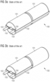
- Figures 1, 2 , 3a and 3b are related to a capacitor according to the state of the art.
- Figures 3a and 3b show a conventional capacitor 100 from a first side ( Figure 3a ) and from the opposite side ( Figure 3b ).
- the capacitor 100 is divided into units Ci (see Figures 1 and 2 ) which are connected in parallel by flat copper bands 102.
- Each capacitance unit Ci contains a capacitance element (winding element 101) and its connections to the copper band 102.
- the winding elements 101 are connected in parallel by the copper bands 102 without any overlap of the copper bands 102.
- the copper bands 102 electrically connect terminals / poles 103 of the winding elements 101.
- the respective copper band 102 is secured to the respective terminal 103 by means of a screw 104.
- the respective copper band 102 extends along an outer side of the capacitor 100 and, in particular, outside a case of the capacitor 100 (external bus bar). In other words, one copper band 102 extends on the first outer side of the capacitor 100 and another copper band 102 extends on the second (opposite) outer side of the capacitor 100.
- FIG. 1 shows a simplified electrical model of the capacitance unit Ci (winding element 101 and its connection to the copper band 102).
- ESRi denotes the parasitic ESR of the capacitance unit Ci
- ESLi denotes the parasitic ESL of the capacitance unit Ci.
- Table 2 requirements for a capacitor in high frequency applications as achieved by capacitors according to the state of the art. Requirements Achieved by state of the art A Low Equivalent Series Resistance (ESR) No B Frequency-stable ESR No C Low Equivalent Series Inductance (ESL) No D Homogeneous internal current distribution No E Internal resonance avoidance No
- FIGs 4 to 9 schematically show a capacitor 1 according to the present invention.
- the capacitor 1 has a round construction.
- the capacitor 1 has a round outer shape.
- the capacitor 1 comprises the outer shape of a cylinder (see, in particular, Figures 4a, 4b , 8 and 9a to 9c ).
- the capacitor 1 is especially adapted to be used in high frequency applications.
- the capacitor 1 comprises a plurality of winding elements 2.
- the capacitor 1 comprises three winding elements 2 ( Figure 4a ).
- the capacitor 1 can comprise more than three winding elements 2, e.g. four, five or six winding elements 2.
- the capacitor 1 can also comprise less than three winding elements 2, e.g. two winding elements 2.
- the number of winding elements 2 is freely selectable.
- the construction described in the following can be implemented with any number of winding elements 2.
- An insulation 9 is arranged between succeeding winding elements 2 as can be seen from Figure 8 .
- the insulation 9 may comprise a polymer, for example.
- the winding elements 2 are axially arranged, i.e. they are arranged along a main longitudinal axis 18 of the capacitor 1.
- the winding elements 2 are electrically connected in parallel.
- a laminated bus bar 3 is provided ( Figure 4b ).
- laminated means that the bus bar 3 comprises several layers (4a, 4b, 5; see, for example, Figure 6 ).
- the said layers which are explained later on in detail, overlap one another at least partly along an outer side of the winding elements 2.
- the bus bar 3 is a (lateral) overlapping bus bar.
- the bus bar 3 extends along the outer side of the winding elements 2 (lateral bus bar).
- the bus bar 3 extends along the outer side of the winding elements 2 from a first end side 10 towards a second end side 11 of the capacitor 1 (see Figure 8 ).
- the bus bar 3 covers the outer side of the respective winding element 2 at least partly. Altogether, the whole bus bar 3 covers between 20 % and 50 % of the outer side of the winding elements 2.
- the bus bar 3 is an internal bus bar. In other words, the bus bar 3 is arranged inside a case 16 of the capacitor 1 (see Figure 9c ).
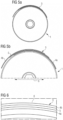
- the bus bar 3 has a round shape which can be taken particularly well from Figure 5a .
- the bus bar 3 comprises the shape of an (incomplete) cylinder shell.
- the bus bar 3 has a shape which is adapted to an outer shape and/or a diameter of the respective winding element 2 and the case 16 of the capacitor 1.
- the bus bar 3 can be used with any number of windings.
- a length (axial extension, i.e. extension along the main longitudinal axis 18 of the capacitor 1) of the bus bar 3 is adapted to the number of winding elements 2.
- the bus bar 3 comprises the previously mentioned layers.
- the bus bar 3 comprises a first layer (first pole) 4a and a second layer (second pole) 4b, which can be gathered from Figures 5b and 6 , for example.
- the layers 4a, 4b comprise copper.
- the layers 4a, 4b comprise a thickness between 0.3 mm and 1.5 mm, preferably 0.5 mm.
- the layers 4a, 4b overlap at least partly.
- the first layer 4a and the second layer 4b are stacked in a radial direction of the capacitor 1.
- a size of the overlap area 6 is such that the overlap area 6 covers between 5 % and 40 % of the outer side of the winding elements 2.
- the overlap area 6 covers 30 % of the outer side of the winding elements 2.
- the layers 4a, 4b are electrically insulated from one another by means of an insulation layer 5.
- the insulation layer 5 comprises a polymer.
- a thickness of the insulation layer 5 is between 0.2 mm and 2.5 mm.
- the thickness of the insulation layer 5 amounts to 0.5 mm.
- the insulation layer 5 is arranged between the first layer 4a and the second layer 4a at least in the overlap area 6 of the two layers 4a, 4b.
- the insulation layer 5 extends beyond the overlap area 6 in an azimuthal and/or axial direction as can be seen from Figure 5b , for example.
- the azimuthal and/or longitudinal extension of the whole bus bar 3 including the layers 4a, 4b and the insulation layer 5 is larger than the azimuthal extension of the overlap area 6 (see for example Figures 7 and 8 ).
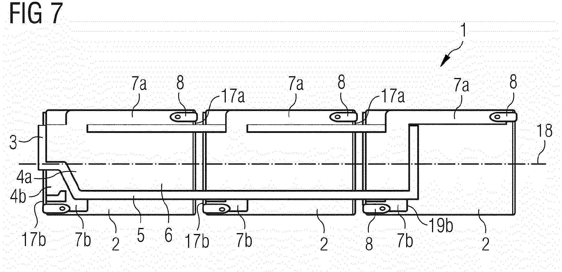
- the first layer 4a is connected to a first pole 17a (e.g. the negative pole) of the respective winding element 2 ( Figure 7 ).
- the second layer 4b is connected to a second pole 17b (e.g. the positive pole) of the respective winding element 2.
- the first layer 4a comprises a plurality of first connection areas 7a.
- the second layer 4b comprises a plurality of second connection areas 7b.
- the respective layer 4a, 4b comprises three respective connection areas 7a, 7b.
- the number of respective connection areas 7a, 7b corresponds to the number of winding elements 2.
- the first connection areas 7a and the first layer 4a are integrally formed.
- the second connection areas 7b and the second layer 4b are integrally formed.
- the respective connection area 7a, 7b is bar shaped.
- the respective connection area 7a, 7b extends parallel to the layers 4a, 4b along the outer surface of the respective winding element 2.
- an intermediate section 19a, 19b (see Figures 7 and 8 ) the respective layer 4a, 4b passes over into the respective connection area 7a, 7b.
- the intermediate section 19a, 19b extends perpendicularly to the connection areas 7a, 7b.
- connection area 7a, 7b is electrically and mechanically connected to the respective pole 17a, 17b of a winding element 2 for connecting the winding elements 2 in parallel.
- the connection areas 7a, 7b are connected to the poles 17a, 17b by means of a connection element 8, e.g. a metal strip ( Figures 7 and 8 ).
- the connection areas 7a, 7b may be soldered to the poles 17a, 17.
- the capacitor 1 further comprises first and second connecting members 12a, 12b ( Figures 8 and 9a ).
- the connecting members 12a, 12b are arranged in the first end region 10 of the capacitor 1.
- the connecting members 12a, 12b comprise metal strips, for example.
- the connecting members 12a, 12b are bent to connect the bus bar 3 arranged on the side surface of the winding elements 2 with the terminals 13a, 13b which are arranged on the first end side 10 of the capacitor 1.
- a terminating member 20 is arranged at the first end side 10 between the winding element 2 and the connecting members 12a, 12b ( Figure 8 ).
- the terminating member 20 comprises an insulating material, e.g. a polymer.
- first connecting member 12a is connected to the first layer 4a of the bus bar 3, e.g. by means of soldering ( Figure 8 and 9a ).
- second connecting member 12b is connected to the second layer 4b of the bus bar 3, e.g. by means of soldering ( Figure 8 and 9a ).
- first connecting member 12a is connected to the first terminal 13a, e.g. by means of a screw or soldering ( Figure 9a ).
- second connecting member 12b is connected to the second terminal 13b, e.g. by means of a screw or soldering ( Figure 9a ).
- An external insulation 14 is arranged on top of the connecting members 12a, 12b on the side surface of the winding elements 2 ( Figure 9b ).
- the external insulation 14 comprises a strip-like shape.
- the external insulation 14 comprises a round shape and extends partly around the outer surface of the winding element 2 arranged close to the first end side 10 of the capacitor 1.
- the external insulation 14 electrically insulates the connecting members 12a, 12b from the case 16 of the capacitor 1 which case 16 is arranged on the external insulation 14 and completely covers the winding elements 2 and the bus bar 3 ( Figure 9c ).
- a cover 15 is arranged on the connecting members 12a, 12b ( Figures 9b and 9c ).
- the cover 15 comprises two cut-outs.
- the cut-outs are adapted and arranged to receive the terminals 13a, 13b.
- the terminals 13a, 13b project from the cut-outs in an axial direction. In this way, an electrical connection of the capacitor 1 is enabled.
- the cover 15 acts as a terminating element of the first end side 10 of the capacitor 1.
- a corresponding cover without cut-outs is arranged on the second side face 11 of the capacitor 1 (not explicitly shown).
- parasitic inductances and resistances ESRi, Rp, Rp2, ESLi, Lp, Lp2
- ESRi, Rp, Rp2, ESLi, Lp, Lp2 ESRi, Rp, Rp2, ESLi, Lp, Lp2
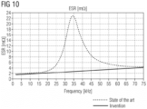
- FIG 10 schematically shows a comparative ESR measurement between the capacitor 100 according to the state of the art ( Figures 3a, 3b ) and the capacitor 1 according to the present disclosure ( Figures 4 to 9 ). It can be observed that in the state of the art, the ESR is less frequency-stable than the ESR of the capacitor according to the present invention. This is due to higher skin effect, non-homogenous internal current distribution and internal resonances in the capacitor design based on the state of the art.
Landscapes
- Engineering & Computer Science (AREA)
- Power Engineering (AREA)
- Manufacturing & Machinery (AREA)
- Microelectronics & Electronic Packaging (AREA)
- Fixed Capacitors And Capacitor Manufacturing Machines (AREA)
Abstract
Description
- The present invention relates to a bus bar for a capacitor. Moreover, the present invention relates to a capacitor comprising the bus bar.
- In high frequency applications, a capacitor has to fulfill the requirements defined in table 1 inside the operation bandwidth.
Table 1: requirements for a capacitor in high frequency applications Requirements A Low Equivalent Series Resistance (ESR) B Frequency-stable ESR C Low Equivalent Series Inductance (ESL) D Homogeneous internal current distribution E Internal resonance avoidance - Overlapped bus bars are used for high frequency applications where a low equivalent series inductance (ESL), low and frequency stable equivalent series resistance (ESR) and a homogeneous internal current distribution are needed. The overlapped bus bar contributes as well to the avoiding of internal resonances between elements.
- Capacitors with round construction are normally divided internally by windings placed axially connected in parallel. The internal construction (round windings and connection elements) are packed in a round case. The round shape of the capacitor makes the use of an internal overlapped bus bar especially complicated from the mechanical point of view.
- Conventionally, the capacitor windings are connected by means of flat bands or wires without any overlapping. This construction has the following disadvantages when good performance at high frequency is requested:
- the operation bandwidth is limited to low frequencies (f < 10 kHz);
- the DC-Link capacitor is divided in several independent capacitors connected in parallel by an external bus bar but if the space is limited and the only dimension of the capacitor that can be increased is the height, the problem cannot be solved with an efficient mechanical solution.
- It is an object of the present disclosure to solve the above mentioned problems. This object is solved by the bus bar and the capacitor according to the independent claims.
- According to a first aspect of the present disclosure, a bus bar is provided. The bus bar is configured to be used in a capacitor. The bus bar is adapted to be integrated in a capacitor, in particular a round capacitor. The bus bar is adapted and arranged for high frequency applications. The bus bar is laminated. In other words, the bus bar is at least partly overlapped. The bus bar is designed such that it comprises a larger width / larger extension perpendicular to a longitudinal axis of the capacitor / larger azimuthal extension than conventional bus bars.
- The bus bar comprises a round shape. For example, the bus bar comprises the shape of a part of a cylinder shell. The bus bar is adapted to an outer shape of the capacitor into which the bus bar is to be integrated. In particular, the bus bar is adapted to the winding shape of the capacitor.
- By means of the laminated bus bar parasitic inductances and resistances (ESRi, Rp, Rp2, ESLi, Lp, Lp2) can be strongly reduced. This makes the bus bar particularly suitable for high frequency applications.
- According to one embodiment, the bus bar comprises a first layer or pole. The bus bar further comprises a second layer or pole. The layers may comprise copper, for example. The layers of the bus bar are adapted and arranged to be connected to poles of a capacitor, in particular to poles of winding elements of the capacitor. The bus bar and, in particular, the layers comprises an overlap area. In the overlap area, the layers of the bus bar overlap one another. In this way, a short and very equilibrated electric connection is facilitated.
- According to one embodiment, an insulation layer is arranged between the first and second layer. The insulation layer may comprise a polymer, for example. The insulation layer is provided at least in the overlap area. In this way, a short circuit between the two layers of the bus bar can be efficiently avoided.
- According to one embodiment, the first layer comprises a plurality of first connection areas. The second layer comprises a plurality of second connection areas. The overlap area of the first layer and the respective first connection area merge into one another. In other words, the first layer and the first connection areas are integrally formed. The overlap area of the second layer and the respective second connection area merge into one another, i.e. the second layer and the second connection areas are integrally formed. Error-prone connections between the overlap area and the connection areas are thus eliminated.
- According to a further aspect, a capacitor is provided. The capacitor is adapted for high frequency applications. The capacitor comprises a plurality of winding elements, e.g. two, three, four or more winding elements. The winding elements are axially arranged, i.e. they are arranged along a main longitudinal axis of the capacitor.
- The capacitor further comprises at least one bus bar. Preferably, the capacitor comprises exactly one bus bar. The bus bar may be the previously described bus bar. Thus, all features described in connection with the bus bar apply for the capacitor as well.
- The capacitor comprises a round shape. The capacitor may comprise the shape of a cylinder. Accordingly, the respective winding element comprises the shape of a cylinder, as well. The laminated / overlapped bus bar is adapted and arranged to connect the winding elements in parallel.
- The laminated bus bar provides a shorter and more equilibrated electric connection of the capacitor and, hence, an improvement of the electrical performance of the capacitor as compared to conventional capacitors. Parasitic inductances and resistances can be strongly reduced, independently of the width of the metallized film of the capacitor. Moreover, considering C homogenous, the impedance (Z) from terminals of the capacitor to each independent winding element is homogenous in all the bandwidth.
- According to one embodiment, the bus bar is arranged inside a case of the capacitor. Accordingly, the bus bar is an internal bus bar. Preferably, the bus bar is arranged on an outer side of the winding elements. Preferably, the bus bar covers between 20 to 50 % of the outer side of the winding elements. The laminated bus bar is very space-saving. In particular, capacitors with the laminated bus bar described above can keep similar dimensions as the one with standard connections (copper bands). Due to the fact that the standard dimensions of the capacitor diameters are kept, a good integration in the power converter is enabled.
- According to one embodiment, the bus bar comprises a first layer or pole. The bus bar further comprises a second layer or pole. The first and second layers are electrically insulated from one another. In particular, the layers are electrically insulated by means of the insulation layer described above.
- The layers of the bus bar extend at least partly along an outer side of the respective winding element. In other words, the bus bar extends on the outer side of the winding elements along the longitudinal axis.
- The bus bar comprises an overlap area. In the overlap area, the layers / poles of the bus bar overlap one another. As the bus bar extends along the longitudinal axis of the capacitor, the bus bar is a laterally overlapped bus bar.
- Preferably, the overlap area of the bus bar covers between 5 % and 40 % of the outer side of the winding elements. In other words, an extension of the bus bar in longitudinal and azimuthal direction is such that the region where the two layers overlap occupies up to 40 % of the outer surface of the winding elements. Thereby, the greater the overlap, the better the compensation of parasitic inductances and resistances. The size of the overlap area depends on the size of the capacitor as well as on the number of windings.
- According to one embodiment, the bus bar has a shape adapted to a diameter of the respective winding element. In particular, the bus bar comprises a round shape, e.g. the shape of a part of a cylinder shell. The bus bar can be used with any numbers of windings. In other words, a length and/or azimuthal extension of the bus bar can be adapted to the size and number of winding elements. Hence, provision of a very flexibly usable bus bar is provided.
- According to one embodiment, the bus bar comprises a plurality of connection areas. In particular, the first layer comprises a plurality of first connection areas. The second layer comprises a plurality of second connection areas. A number of first connection areas corresponds to a number of winding elements. Moreover, a number of second connection areas corresponds to the number of winding elements.
- The connection areas are adapted and arranged to be electrically and mechanically connected to poles of the winding elements. The connection areas may be soldered to the poles of the winding elements. Accordingly, the first layer may be connected to a first pole of a respective winding element. The second layer may be connected to a second pole of the respective winding element. Hence, a short and very equilibrated electric connection between the bus bar and the poles is enabled. In this way, the electrical performance of the capacitor is increased.
- Further features, refinements and expediencies become apparent from the following description of the exemplary embodiments in connection with the figures.
-
Figure 1 schematically shows a simplified electrical model of a capacitance unit according to the state of the art, -
Figure 2 schematically shows a simplified electrical model of a DC-Link capacitor according to the state of the art, -
Figures 3a and 3b schematically show a perspective view of a capacitor according to the state of the art, -
Figures 4a and 4a schematically show a perspective view of parts of a capacitor, -
Figures 5a and 5b schematically show a sectional view of a part of a capacitor, -
Figure 6 schematically shows a sectional view of a part of a capacitor, -
Figure 7 schematically shows a perspective view of a part of a capacitor, -
Figure 8 schematically shows a perspective view of the capacitor according toFigure 7 , -
Figures 9a to 9c schematically show a perspective view of parts of the capacitor according toFigures 7 and 8 , -
Figure 10 schematically shows a comparative ESR measurement between a capacitor according to the state of the art and the capacitor according to the present disclosure. -
Figures 1, 2 ,3a and 3b are related to a capacitor according to the state of the art. In particular,Figures 3a and 3b show aconventional capacitor 100 from a first side (Figure 3a ) and from the opposite side (Figure 3b ). Thecapacitor 100 is divided into units Ci (seeFigures 1 and 2 ) which are connected in parallel byflat copper bands 102. Each capacitance unit Ci contains a capacitance element (winding element 101) and its connections to thecopper band 102. - The winding
elements 101 are connected in parallel by thecopper bands 102 without any overlap of thecopper bands 102. Thecopper bands 102 electrically connect terminals /poles 103 of the windingelements 101. Therespective copper band 102 is secured to therespective terminal 103 by means of ascrew 104. Therespective copper band 102 extends along an outer side of thecapacitor 100 and, in particular, outside a case of the capacitor 100 (external bus bar). In other words, onecopper band 102 extends on the first outer side of thecapacitor 100 and anothercopper band 102 extends on the second (opposite) outer side of thecapacitor 100. - In this context,
Figure 1 shows a simplified electrical model of the capacitance unit Ci (windingelement 101 and its connection to the copper band 102). Thereby, ESRi denotes the parasitic ESR of the capacitance unit Ci and ESLi denotes the parasitic ESL of the capacitance unit Ci. - A simplified electrical model of a complete DC-Link capacitor (with a plurality of capacitance units Ci) is shown in
Figure 2 , where - Ci: capacitance unit - capacitance value,
- ESRi: capacitance unit - parasitic ESR,
- ESLi: capacitance unit - parasitic ESL,
- Cp: connectors between capacitance units - parasitic capacitance,
- Rp, Rp2: connectors between capacitance units - parasitic resistance,
- Lp, Lp2: connectors between capacitance units - parasitic inductance,
- Rt: terminal - parasitic resistance,
- Lt: terminal - parasitic inductance.
- The electrical requirements achieved with this solution are summarized in table 2.
Table 2: requirements for a capacitor in high frequency applications as achieved by capacitors according to the state of the art. Requirements Achieved by state of the art A Low Equivalent Series Resistance (ESR) No B Frequency-stable ESR No C Low Equivalent Series Inductance (ESL) No D Homogeneous internal current distribution No E Internal resonance avoidance No -
Figures 4 to 9 schematically show acapacitor 1 according to the present invention. Thecapacitor 1 has a round construction. In other words, thecapacitor 1 has a round outer shape. In particular, thecapacitor 1 comprises the outer shape of a cylinder (see, in particular,Figures 4a, 4b ,8 and9a to 9c ). Thecapacitor 1 is especially adapted to be used in high frequency applications. - The
capacitor 1 comprises a plurality of windingelements 2. In this embodiment, thecapacitor 1 comprises three winding elements 2 (Figure 4a ). Of course, thecapacitor 1 can comprise more than three windingelements 2, e.g. four, five or six windingelements 2. Thecapacitor 1 can also comprise less than three windingelements 2, e.g. two windingelements 2. In particular, the number of windingelements 2 is freely selectable. In other words, the construction described in the following can be implemented with any number of windingelements 2. An insulation 9 is arranged between succeeding windingelements 2 as can be seen fromFigure 8 . The insulation 9 may comprise a polymer, for example. - The winding
elements 2 are axially arranged, i.e. they are arranged along a mainlongitudinal axis 18 of thecapacitor 1. The windingelements 2 are electrically connected in parallel. For this purpose, alaminated bus bar 3 is provided (Figure 4b ). In this context, the term "laminated" means that thebus bar 3 comprises several layers (4a, 4b, 5; see, for example,Figure 6 ). The said layers, which are explained later on in detail, overlap one another at least partly along an outer side of the windingelements 2. In other words, thebus bar 3 is a (lateral) overlapping bus bar. - As can be seen from
Figure 4b , thebus bar 3 extends along the outer side of the winding elements 2 (lateral bus bar). Thebus bar 3 extends along the outer side of the windingelements 2 from afirst end side 10 towards asecond end side 11 of the capacitor 1 (seeFigure 8 ). Thebus bar 3 covers the outer side of the respective windingelement 2 at least partly. Altogether, thewhole bus bar 3 covers between 20 % and 50 % of the outer side of the windingelements 2. Thebus bar 3 is an internal bus bar. In other words, thebus bar 3 is arranged inside acase 16 of the capacitor 1 (seeFigure 9c ). - The
bus bar 3 has a round shape which can be taken particularly well fromFigure 5a . Thebus bar 3 comprises the shape of an (incomplete) cylinder shell. Thebus bar 3 has a shape which is adapted to an outer shape and/or a diameter of the respective windingelement 2 and thecase 16 of thecapacitor 1. Thebus bar 3 can be used with any number of windings. A length (axial extension, i.e. extension along the mainlongitudinal axis 18 of the capacitor 1) of thebus bar 3 is adapted to the number of windingelements 2. - The
bus bar 3 comprises the previously mentioned layers. In particular, thebus bar 3 comprises a first layer (first pole) 4a and a second layer (second pole) 4b, which can be gathered fromFigures 5b and 6 , for example. Thelayers layers - The
layers first layer 4a and thesecond layer 4b are stacked in a radial direction of thecapacitor 1. A size of the overlap area 6 (axial and azimuthal extension) is such that theoverlap area 6 covers between 5 % and 40 % of the outer side of the windingelements 2. Preferably, theoverlap area 6 covers 30 % of the outer side of the windingelements 2. - The
layers insulation layer 5. Theinsulation layer 5 comprises a polymer. A thickness of theinsulation layer 5 is between 0.2 mm and 2.5 mm. Preferably, the thickness of theinsulation layer 5 amounts to 0.5 mm. - The
insulation layer 5 is arranged between thefirst layer 4a and thesecond layer 4a at least in theoverlap area 6 of the twolayers insulation layer 5 extends beyond theoverlap area 6 in an azimuthal and/or axial direction as can be seen fromFigure 5b , for example. In other words, the azimuthal and/or longitudinal extension of thewhole bus bar 3 including thelayers insulation layer 5 is larger than the azimuthal extension of the overlap area 6 (see for exampleFigures 7 and 8 ). - The
first layer 4a is connected to afirst pole 17a (e.g. the negative pole) of the respective winding element 2 (Figure 7 ). Thesecond layer 4b is connected to asecond pole 17b (e.g. the positive pole) of the respective windingelement 2. - For this purpose, the
first layer 4a comprises a plurality offirst connection areas 7a. Thesecond layer 4b comprises a plurality ofsecond connection areas 7b. In this embodiment, therespective layer respective connection areas respective connection areas elements 2. - The
first connection areas 7a and thefirst layer 4a are integrally formed. Thesecond connection areas 7b and thesecond layer 4b are integrally formed. Therespective connection area respective connection area layers element 2. In anintermediate section Figures 7 and 8 ), therespective layer respective connection area intermediate section connection areas - The
respective connection area respective pole element 2 for connecting the windingelements 2 in parallel. Theconnection areas poles connection element 8, e.g. a metal strip (Figures 7 and 8 ). Theconnection areas poles 17a, 17. - For electrically and mechanically connecting the
bus bar 3 toterminals capacitor 1, thecapacitor 1 further comprises first and second connectingmembers Figures 8 and9a ). The connectingmembers first end region 10 of thecapacitor 1. The connectingmembers members bus bar 3 arranged on the side surface of the windingelements 2 with theterminals first end side 10 of thecapacitor 1. A terminatingmember 20 is arranged at thefirst end side 10 between the windingelement 2 and the connectingmembers Figure 8 ). The terminatingmember 20 comprises an insulating material, e.g. a polymer. - In a first end section, the first connecting
member 12a is connected to thefirst layer 4a of thebus bar 3, e.g. by means of soldering (Figure 8 and9a ). Likewise, in a first end section, the second connectingmember 12b is connected to thesecond layer 4b of thebus bar 3, e.g. by means of soldering (Figure 8 and9a ). - In a second or opposite end section, the first connecting
member 12a is connected to thefirst terminal 13a, e.g. by means of a screw or soldering (Figure 9a ). Likewise, in a second or opposite end section, the second connectingmember 12b is connected to thesecond terminal 13b, e.g. by means of a screw or soldering (Figure 9a ). - An
external insulation 14 is arranged on top of the connectingmembers Figure 9b ). Theexternal insulation 14 comprises a strip-like shape. Theexternal insulation 14 comprises a round shape and extends partly around the outer surface of the windingelement 2 arranged close to thefirst end side 10 of thecapacitor 1. Theexternal insulation 14 electrically insulates the connectingmembers case 16 of thecapacitor 1 whichcase 16 is arranged on theexternal insulation 14 and completely covers the windingelements 2 and the bus bar 3 (Figure 9c ). - Moreover, on the first end side 10 a
cover 15 is arranged on the connectingmembers Figures 9b and 9c ). Thecover 15 comprises two cut-outs. The cut-outs are adapted and arranged to receive theterminals terminals capacitor 1 is enabled. Thecover 15 acts as a terminating element of thefirst end side 10 of thecapacitor 1. A corresponding cover without cut-outs is arranged on thesecond side face 11 of the capacitor 1 (not explicitly shown). - By means of the construction as described above parasitic inductances and resistances (ESRi, Rp, Rp2, ESLi, Lp, Lp2) can be strongly reduced, independently of the width of the metallized film of the capacitor. Moreover, considering C to be homogenous, the impedance from the
terminals Table 3: requirements for a capacitor in high frequency applications as achieved by capacitors according to the state of the art in comparison to the capacitor according to the present invention. Requirements Achieved by state of the art Achieved by present invention A Low Equivalent Series Resistance (ESR) No Yes B Frequency-stable ESR No Yes C Low Equivalent Series Inductance (ESL) No Yes D Homogeneous internal current distribution No Yes E Internal resonance avoidance No Yes -
Figure 10 schematically shows a comparative ESR measurement between thecapacitor 100 according to the state of the art (Figures 3a, 3b ) and thecapacitor 1 according to the present disclosure (Figures 4 to 9 ). It can be observed that in the state of the art, the ESR is less frequency-stable than the ESR of the capacitor according to the present invention. This is due to higher skin effect, non-homogenous internal current distribution and internal resonances in the capacitor design based on the state of the art. - In the figures, elements of the same structure and / or functionality may be referenced by the same reference numerals. It is to be understood that the embodiments shown in the figures are illustrative representations and are not necessarily drawn to scale.
-
- 1
- Capacitor
- 2
- Winding element
- 3
- Bus bar
- 4a
- First layer
- 4b
- Second layer
- 5
- Insulation layer
- 6
- Overlap area
- 7a
- First connection area
- 7b
- Second connection area
- 8
- Connection element
- 9
- Insulation
- 10
- First end side of capacitor
- 11
- Second end side of capacitor
- 12a
- First connecting member
- 12b
- Second connecting member
- 13a
- First terminal
- 13b
- Second terminal
- 14
- Insulating element
- 15
- Cover
- 16
- Case
- 17a
- First pole
- 17b
- Second pole
- 18
- Main longitudinal axis
- 19a
- First intermediate section
- 19b
- Second intermediate section
- 20
- Terminating element
- 100
- Capacitor
- 101
- Winding element
- 102
- Copper band
- 103
- Terminal
- 104
- Screw
- Ci
- Capacitance unit - capacitance value
- ESRi
- Capacitance unit - parasitic ESR
- ESLi
- Capacitance unit - parasitic ESL
- Cp
- Connectors between capacitance units - parasitic capacitance
- Rp, Rp2
- Connectors between capacitance units - parasitic resistance
- Lp, Lp2
- Connectors between capacitance units - parasitic inductance
- Rt
- Terminal - parasitic resistance
- Lt
- Terminal - parasitic inductance
Claims (12)
- Bus bar (3) for a capacitor (1),
wherein the bus bar (3) is laminated and wherein the bus bar (3) comprises a round shape. - Bus bar (3) according to claim 1,
comprising a first layer (4a) and a second layer (4b) adapted and arranged to be connected to poles (17a, 17b) of a capacitor (1), wherein the bus bar (3) comprises an overlap area (6) in which the layers (4a, 4b) overlap one another. - Bus bar (3) according to claim 2,
wherein an insulation layer (5) is arranged between the first and second layer (4a, 4b) at least in the overlap area (6). - Bus bar (3) according to claim 2 or claim 3,
wherein the first layer (4a) comprises a plurality of first connection areas (7a) and the second layer (4b) comprises a plurality of second connection areas (7b), wherein the overlap area (6) of the first layer (4a) and the respective first connection area (7a) merge into one another, and wherein the overlap area (6) of the second layer (4b) and the respective second connection area (7b) merge into one another. - Bus bar (3) according to any of the previous claims,
wherein the bus bar (3) is adapted and arranged for high frequency applications. - Capacitor (1) comprising- a plurality of winding elements (2),- at least one bus bar (3) according to any one of the previous claims,wherein the capacitor (1) comprises a round shape and wherein the bus bar (3) is adapted and arranged to connect the winding elements (2) in parallel.
- Capacitor (1) according to claim 6,
wherein the bus bar (3) is arranged inside a case (16) of the capacitor (1). - Capacitor (1) according to claim 6 or claim 7,
wherein the bus bar (3) comprises a first layer (4a) and a second layer (4b) extending at least partly along an outer side of the respective winding element (2), wherein the bus bar (3) comprises an overlap area (6) in which the layers (4a, 4b) overlap one another. - Capacitor (1) according to any of claims 6 to 8,
wherein the bus bar (3) has a shape adapted to a diameter of the respective winding element (2). - Capacitor (1) according to any of claims 6 to 9,
wherein the bus bar (3) comprises a plurality of connection areas (7a, 7b) adapted and arranged to be electrically and mechanically connected to poles (17a, 17b) of the winding elements (2). - Capacitor (1) according to claim 10,
wherein the respective connection area (7a, 7b) is soldered to the respective pole (17a, 17b) of a winding element (2). - Capacitor (1) according to claim 10 or claim 11,
wherein a number of first connection areas (7a) corresponds to a number of winding elements (2) and wherein a number of second connection areas (7b) corresponds to the number of winding elements (2).
Priority Applications (6)
| Application Number | Priority Date | Filing Date | Title |
|---|---|---|---|
| EP21383040.9A EP4184538A1 (en) | 2021-11-17 | 2021-11-17 | Laminated round busbar for capacitor assembly |
| EP26165803.3A EP4734133A2 (en) | 2021-11-17 | 2021-11-17 | Bus bar for a capacitor and capacitor |
| US18/710,483 US20250014826A1 (en) | 2021-11-17 | 2022-10-11 | Bus bar for a capacitor and capacitor |
| JP2024529437A JP2024539444A (en) | 2021-11-17 | 2022-10-11 | Capacitor busbar and capacitor |
| PCT/EP2022/078208 WO2023088613A1 (en) | 2021-11-17 | 2022-10-11 | Bus bar for a capacitor and capacitor |
| EP22800667.2A EP4434066A1 (en) | 2021-11-17 | 2022-10-11 | Bus bar for a capacitor and capacitor |
Applications Claiming Priority (1)
| Application Number | Priority Date | Filing Date | Title |
|---|---|---|---|
| EP21383040.9A EP4184538A1 (en) | 2021-11-17 | 2021-11-17 | Laminated round busbar for capacitor assembly |
Related Child Applications (1)
| Application Number | Title | Priority Date | Filing Date |
|---|---|---|---|
| EP26165803.3A Division EP4734133A2 (en) | 2021-11-17 | 2021-11-17 | Bus bar for a capacitor and capacitor |
Publications (1)
| Publication Number | Publication Date |
|---|---|
| EP4184538A1 true EP4184538A1 (en) | 2023-05-24 |
Family
ID=78770574
Family Applications (3)
| Application Number | Title | Priority Date | Filing Date |
|---|---|---|---|
| EP21383040.9A Pending EP4184538A1 (en) | 2021-11-17 | 2021-11-17 | Laminated round busbar for capacitor assembly |
| EP26165803.3A Pending EP4734133A2 (en) | 2021-11-17 | 2021-11-17 | Bus bar for a capacitor and capacitor |
| EP22800667.2A Pending EP4434066A1 (en) | 2021-11-17 | 2022-10-11 | Bus bar for a capacitor and capacitor |
Family Applications After (2)
| Application Number | Title | Priority Date | Filing Date |
|---|---|---|---|
| EP26165803.3A Pending EP4734133A2 (en) | 2021-11-17 | 2021-11-17 | Bus bar for a capacitor and capacitor |
| EP22800667.2A Pending EP4434066A1 (en) | 2021-11-17 | 2022-10-11 | Bus bar for a capacitor and capacitor |
Country Status (4)
| Country | Link |
|---|---|
| US (1) | US20250014826A1 (en) |
| EP (3) | EP4184538A1 (en) |
| JP (1) | JP2024539444A (en) |
| WO (1) | WO2023088613A1 (en) |
Citations (2)
| Publication number | Priority date | Publication date | Assignee | Title |
|---|---|---|---|---|
| CN204407189U (en) * | 2015-03-17 | 2015-06-17 | 常州常捷科技有限公司 | A kind of metallic film filter capacitor |
| CN111048304A (en) * | 2019-12-31 | 2020-04-21 | 西安西电电力电容器有限责任公司 | Electrode structure and capacitor for cylindrical capacitor |
Family Cites Families (7)
| Publication number | Priority date | Publication date | Assignee | Title |
|---|---|---|---|---|
| JP4419416B2 (en) * | 2003-03-31 | 2010-02-24 | パナソニック株式会社 | Metallized film capacitors |
| US7864506B2 (en) * | 2007-11-30 | 2011-01-04 | Hamilton Sundstrand Corporation | System and method of film capacitor cooling |
| JP5424030B2 (en) * | 2009-08-31 | 2014-02-26 | 株式会社指月電機製作所 | Capacitor |
| JP2013251351A (en) * | 2012-05-31 | 2013-12-12 | Meidensha Corp | Capacitor |
| CN203966836U (en) * | 2014-06-25 | 2014-11-26 | 佛山市顺德区创格电子实业有限公司 | The film capacitor that dendritic is connected in parallel |
| CN104766722B (en) * | 2015-03-17 | 2018-04-13 | 常州常捷科技有限公司 | Metallic film filter capacitor with low inductance low ESR characteristic |
| DE102018117283B3 (en) * | 2018-06-13 | 2019-11-14 | Electronicon Kondensatoren Gmbh | Contact arrangement for front sides of capacitor windings |
-
2021
- 2021-11-17 EP EP21383040.9A patent/EP4184538A1/en active Pending
- 2021-11-17 EP EP26165803.3A patent/EP4734133A2/en active Pending
-
2022
- 2022-10-11 EP EP22800667.2A patent/EP4434066A1/en active Pending
- 2022-10-11 US US18/710,483 patent/US20250014826A1/en active Pending
- 2022-10-11 JP JP2024529437A patent/JP2024539444A/en active Pending
- 2022-10-11 WO PCT/EP2022/078208 patent/WO2023088613A1/en not_active Ceased
Patent Citations (2)
| Publication number | Priority date | Publication date | Assignee | Title |
|---|---|---|---|---|
| CN204407189U (en) * | 2015-03-17 | 2015-06-17 | 常州常捷科技有限公司 | A kind of metallic film filter capacitor |
| CN111048304A (en) * | 2019-12-31 | 2020-04-21 | 西安西电电力电容器有限责任公司 | Electrode structure and capacitor for cylindrical capacitor |
Also Published As
| Publication number | Publication date |
|---|---|
| US20250014826A1 (en) | 2025-01-09 |
| EP4434066A1 (en) | 2024-09-25 |
| EP4734133A2 (en) | 2026-04-29 |
| JP2024539444A (en) | 2024-10-28 |
| WO2023088613A1 (en) | 2023-05-25 |
Similar Documents
| Publication | Publication Date | Title |
|---|---|---|
| JP3914865B2 (en) | Metallized film capacitors | |
| TWI338903B (en) | Ultra low inductance multi layer ceramic capacitor | |
| US8421557B2 (en) | Chip-type solid electrolytic capacitor and chip-type filter | |
| US9627140B2 (en) | Capacitor component | |
| KR100706454B1 (en) | Chip type solid electrolyte capacitor and method of manufacturing the same | |
| JP4475338B2 (en) | Multilayer capacitor | |
| US7619873B2 (en) | Feedthrough multilayer capacitor | |
| US7388738B1 (en) | Multilayer capacitor | |
| CN114068182A (en) | Non-inductive film capacitor and manufacturing method thereof | |
| JP3583034B2 (en) | Low inductance capacitor | |
| JP2003332173A (en) | Capacitor element, solid electrolytic capacitor and capacitor built-in substrate | |
| US20250014826A1 (en) | Bus bar for a capacitor and capacitor | |
| JP5093044B2 (en) | Multilayer capacitor | |
| WO2001022450A1 (en) | Electrical capacitor with improved heat transfer characteristics | |
| TW202244962A (en) | Capacitor assembly package structure, and capacitor element and method of manufacturing the same | |
| CN116137207B (en) | Bus bar for capacitor and capacitor | |
| CN113574620A (en) | Capacitor, in particular intermediate circuit capacitor for multiphase systems | |
| JP2002043166A (en) | Electronic components | |
| JP4803749B2 (en) | Metallized film capacitors | |
| US12283425B2 (en) | Capacitor assembly | |
| CN221805323U (en) | Cylindrical capacitor | |
| CN117678041A (en) | Capacitor components | |
| JP5077180B2 (en) | Multilayer capacitor | |
| JPH041718Y2 (en) | ||
| JP2025006220A (en) | Composite Parts |
Legal Events
| Date | Code | Title | Description |
|---|---|---|---|
| PUAI | Public reference made under article 153(3) epc to a published international application that has entered the european phase |
Free format text: ORIGINAL CODE: 0009012 |
|
| STAA | Information on the status of an ep patent application or granted ep patent |
Free format text: STATUS: THE APPLICATION HAS BEEN PUBLISHED |
|
| AK | Designated contracting states |
Kind code of ref document: A1 Designated state(s): AL AT BE BG CH CY CZ DE DK EE ES FI FR GB GR HR HU IE IS IT LI LT LU LV MC MK MT NL NO PL PT RO RS SE SI SK SM TR |
|
| STAA | Information on the status of an ep patent application or granted ep patent |
Free format text: STATUS: REQUEST FOR EXAMINATION WAS MADE |
|
| 17P | Request for examination filed |
Effective date: 20230712 |
|
| RBV | Designated contracting states (corrected) |
Designated state(s): AL AT BE BG CH CY CZ DE DK EE ES FI FR GB GR HR HU IE IS IT LI LT LU LV MC MK MT NL NO PL PT RO RS SE SI SK SM TR |
|
| GRAP | Despatch of communication of intention to grant a patent |
Free format text: ORIGINAL CODE: EPIDOSNIGR1 |
|
| STAA | Information on the status of an ep patent application or granted ep patent |
Free format text: STATUS: GRANT OF PATENT IS INTENDED |
|
| GRAJ | Information related to disapproval of communication of intention to grant by the applicant or resumption of examination proceedings by the epo deleted |
Free format text: ORIGINAL CODE: EPIDOSDIGR1 |
|
| STAA | Information on the status of an ep patent application or granted ep patent |
Free format text: STATUS: REQUEST FOR EXAMINATION WAS MADE |
|
| GRAP | Despatch of communication of intention to grant a patent |
Free format text: ORIGINAL CODE: EPIDOSNIGR1 |
|
| STAA | Information on the status of an ep patent application or granted ep patent |
Free format text: STATUS: GRANT OF PATENT IS INTENDED |
|
| INTG | Intention to grant announced |
Effective date: 20260109 |
|
| INTC | Intention to grant announced (deleted) | ||
| INTG | Intention to grant announced |
Effective date: 20260205 |