EP4183894A1 - Method for surface treatment of an electrical contact element and contact element - Google Patents
Method for surface treatment of an electrical contact element and contact element Download PDFInfo
- Publication number
- EP4183894A1 EP4183894A1 EP22208081.4A EP22208081A EP4183894A1 EP 4183894 A1 EP4183894 A1 EP 4183894A1 EP 22208081 A EP22208081 A EP 22208081A EP 4183894 A1 EP4183894 A1 EP 4183894A1
- Authority
- EP
- European Patent Office
- Prior art keywords
- electrically conductive
- contact element
- contact surface
- plasma
- conductive contact
- Prior art date
- Legal status (The legal status is an assumption and is not a legal conclusion. Google has not performed a legal analysis and makes no representation as to the accuracy of the status listed.)
- Pending
Links
- 238000000034 method Methods 0.000 title claims abstract description 44
- 238000004381 surface treatment Methods 0.000 title abstract description 10
- 239000000314 lubricant Substances 0.000 claims abstract description 49
- 239000007787 solid Substances 0.000 claims abstract description 26
- 238000009832 plasma treatment Methods 0.000 claims abstract description 22
- 239000011248 coating agent Substances 0.000 claims abstract description 17
- 238000000576 coating method Methods 0.000 claims abstract description 17
- 230000013011 mating Effects 0.000 claims description 49
- 239000000463 material Substances 0.000 claims description 28
- PXHVJJICTQNCMI-UHFFFAOYSA-N Nickel Chemical compound [Ni] PXHVJJICTQNCMI-UHFFFAOYSA-N 0.000 claims description 18
- RYGMFSIKBFXOCR-UHFFFAOYSA-N Copper Chemical compound [Cu] RYGMFSIKBFXOCR-UHFFFAOYSA-N 0.000 claims description 9
- 239000010949 copper Substances 0.000 claims description 9
- 239000004332 silver Substances 0.000 claims description 8
- 229910052802 copper Inorganic materials 0.000 claims description 7
- 229910052759 nickel Inorganic materials 0.000 claims description 7
- BQCADISMDOOEFD-UHFFFAOYSA-N Silver Chemical compound [Ag] BQCADISMDOOEFD-UHFFFAOYSA-N 0.000 claims description 6
- 239000002253 acid Substances 0.000 claims description 6
- 229910052709 silver Inorganic materials 0.000 claims description 6
- ATJFFYVFTNAWJD-UHFFFAOYSA-N Tin Chemical compound [Sn] ATJFFYVFTNAWJD-UHFFFAOYSA-N 0.000 claims description 5
- 238000005260 corrosion Methods 0.000 claims description 5
- 230000007797 corrosion Effects 0.000 claims description 5
- 229910052718 tin Inorganic materials 0.000 claims description 5
- 229910001128 Sn alloy Inorganic materials 0.000 claims description 4
- 150000007513 acids Chemical class 0.000 claims description 4
- 239000003963 antioxidant agent Substances 0.000 claims description 4
- 239000003112 inhibitor Substances 0.000 claims description 4
- 238000010924 continuous production Methods 0.000 claims description 3
- OKTJSMMVPCPJKN-UHFFFAOYSA-N Carbon Chemical compound [C] OKTJSMMVPCPJKN-UHFFFAOYSA-N 0.000 description 17
- 229910052799 carbon Inorganic materials 0.000 description 8
- 238000011161 development Methods 0.000 description 8
- 238000005259 measurement Methods 0.000 description 6
- 229910002804 graphite Inorganic materials 0.000 description 5
- 239000010439 graphite Substances 0.000 description 5
- 239000000203 mixture Substances 0.000 description 5
- 239000000126 substance Substances 0.000 description 5
- IJGRMHOSHXDMSA-UHFFFAOYSA-N Atomic nitrogen Chemical compound N#N IJGRMHOSHXDMSA-UHFFFAOYSA-N 0.000 description 4
- 239000002041 carbon nanotube Substances 0.000 description 4
- 229910021393 carbon nanotube Inorganic materials 0.000 description 4
- 239000007789 gas Substances 0.000 description 4
- 239000004519 grease Substances 0.000 description 4
- 230000001050 lubricating effect Effects 0.000 description 4
- 229910052961 molybdenite Inorganic materials 0.000 description 4
- CWQXQMHSOZUFJS-UHFFFAOYSA-N molybdenum disulfide Chemical compound S=[Mo]=S CWQXQMHSOZUFJS-UHFFFAOYSA-N 0.000 description 4
- 229910052982 molybdenum disulfide Inorganic materials 0.000 description 4
- 239000011135 tin Substances 0.000 description 4
- 238000005299 abrasion Methods 0.000 description 3
- 230000000694 effects Effects 0.000 description 3
- 229910001316 Ag alloy Inorganic materials 0.000 description 2
- XKRFYHLGVUSROY-UHFFFAOYSA-N Argon Chemical compound [Ar] XKRFYHLGVUSROY-UHFFFAOYSA-N 0.000 description 2
- 229910000881 Cu alloy Inorganic materials 0.000 description 2
- 229910000990 Ni alloy Inorganic materials 0.000 description 2
- 238000007373 indentation Methods 0.000 description 2
- 229910052757 nitrogen Inorganic materials 0.000 description 2
- UCKMPCXJQFINFW-UHFFFAOYSA-N Sulphide Chemical compound [S-2] UCKMPCXJQFINFW-UHFFFAOYSA-N 0.000 description 1
- 239000000654 additive Substances 0.000 description 1
- 230000000996 additive effect Effects 0.000 description 1
- 230000002411 adverse Effects 0.000 description 1
- 229910045601 alloy Inorganic materials 0.000 description 1
- 239000000956 alloy Substances 0.000 description 1
- 229910052786 argon Inorganic materials 0.000 description 1
- 238000000418 atomic force spectrum Methods 0.000 description 1
- 239000010953 base metal Substances 0.000 description 1
- 230000005540 biological transmission Effects 0.000 description 1
- -1 carbonaceous Chemical compound 0.000 description 1
- 238000012512 characterization method Methods 0.000 description 1
- 229910052729 chemical element Inorganic materials 0.000 description 1
- 239000013078 crystal Substances 0.000 description 1
- 230000001419 dependent effect Effects 0.000 description 1
- 238000009826 distribution Methods 0.000 description 1
- 230000007613 environmental effect Effects 0.000 description 1
- 238000011156 evaluation Methods 0.000 description 1
- 231100001261 hazardous Toxicity 0.000 description 1
- 239000001257 hydrogen Substances 0.000 description 1
- 229910052739 hydrogen Inorganic materials 0.000 description 1
- 125000004435 hydrogen atom Chemical class [H]* 0.000 description 1
- 235000013902 inosinic acid Nutrition 0.000 description 1
- 230000010354 integration Effects 0.000 description 1
- 238000011835 investigation Methods 0.000 description 1
- JEIPFZHSYJVQDO-UHFFFAOYSA-N iron(III) oxide Inorganic materials O=[Fe]O[Fe]=O JEIPFZHSYJVQDO-UHFFFAOYSA-N 0.000 description 1
- 239000007788 liquid Substances 0.000 description 1
- 238000012423 maintenance Methods 0.000 description 1
- 238000004519 manufacturing process Methods 0.000 description 1
- 238000000691 measurement method Methods 0.000 description 1
- 238000012544 monitoring process Methods 0.000 description 1
- ORQBXQOJMQIAOY-UHFFFAOYSA-N nobelium Chemical compound [No] ORQBXQOJMQIAOY-UHFFFAOYSA-N 0.000 description 1
- 229910000510 noble metal Inorganic materials 0.000 description 1
- 230000003287 optical effect Effects 0.000 description 1
- 230000008092 positive effect Effects 0.000 description 1
- 230000005855 radiation Effects 0.000 description 1
- 230000008054 signal transmission Effects 0.000 description 1
- 230000003746 surface roughness Effects 0.000 description 1
- 238000003466 welding Methods 0.000 description 1
Images
Classifications
-
- C—CHEMISTRY; METALLURGY
- C23—COATING METALLIC MATERIAL; COATING MATERIAL WITH METALLIC MATERIAL; CHEMICAL SURFACE TREATMENT; DIFFUSION TREATMENT OF METALLIC MATERIAL; COATING BY VACUUM EVAPORATION, BY SPUTTERING, BY ION IMPLANTATION OR BY CHEMICAL VAPOUR DEPOSITION, IN GENERAL; INHIBITING CORROSION OF METALLIC MATERIAL OR INCRUSTATION IN GENERAL
- C23C—COATING METALLIC MATERIAL; COATING MATERIAL WITH METALLIC MATERIAL; SURFACE TREATMENT OF METALLIC MATERIAL BY DIFFUSION INTO THE SURFACE, BY CHEMICAL CONVERSION OR SUBSTITUTION; COATING BY VACUUM EVAPORATION, BY SPUTTERING, BY ION IMPLANTATION OR BY CHEMICAL VAPOUR DEPOSITION, IN GENERAL
- C23C24/00—Coating starting from inorganic powder
- C23C24/08—Coating starting from inorganic powder by application of heat or pressure and heat
- C23C24/10—Coating starting from inorganic powder by application of heat or pressure and heat with intermediate formation of a liquid phase in the layer
-
- H—ELECTRICITY
- H01—ELECTRIC ELEMENTS
- H01R—ELECTRICALLY-CONDUCTIVE CONNECTIONS; STRUCTURAL ASSOCIATIONS OF A PLURALITY OF MUTUALLY-INSULATED ELECTRICAL CONNECTING ELEMENTS; COUPLING DEVICES; CURRENT COLLECTORS
- H01R43/00—Apparatus or processes specially adapted for manufacturing, assembling, maintaining, or repairing of line connectors or current collectors or for joining electric conductors
- H01R43/16—Apparatus or processes specially adapted for manufacturing, assembling, maintaining, or repairing of line connectors or current collectors or for joining electric conductors for manufacturing contact members, e.g. by punching and by bending
-
- H—ELECTRICITY
- H01—ELECTRIC ELEMENTS
- H01R—ELECTRICALLY-CONDUCTIVE CONNECTIONS; STRUCTURAL ASSOCIATIONS OF A PLURALITY OF MUTUALLY-INSULATED ELECTRICAL CONNECTING ELEMENTS; COUPLING DEVICES; CURRENT COLLECTORS
- H01R13/00—Details of coupling devices of the kinds covered by groups H01R12/70 or H01R24/00 - H01R33/00
- H01R13/02—Contact members
- H01R13/03—Contact members characterised by the material, e.g. plating, or coating materials
-
- H—ELECTRICITY
- H01—ELECTRIC ELEMENTS
- H01R—ELECTRICALLY-CONDUCTIVE CONNECTIONS; STRUCTURAL ASSOCIATIONS OF A PLURALITY OF MUTUALLY-INSULATED ELECTRICAL CONNECTING ELEMENTS; COUPLING DEVICES; CURRENT COLLECTORS
- H01R2201/00—Connectors or connections adapted for particular applications
- H01R2201/26—Connectors or connections adapted for particular applications for vehicles
Definitions
- the present invention relates to a method for surface treatment of an electrically conductive contact element for an electrical connector. Furthermore, the invention relates to an electrically conductive contact element whose surface is treated by means of such a method.
- Electrical connectors and their contact elements are known in numerous designs. Electrical connectors are intended to be mated with a suitable mating connector to establish an electrical connection. Electrical connectors are generally used either for signal transmission or for power transmission. For this purpose, electrical connectors generally have electrically conductive contact elements that come into contact with a contact element of the mating connector when the connector is mated. Frequently, the contact elements of one connector element are designed as contact pins and those of the mating connector as contact springs. When the connector and mating connector are mated, the contact springs exert elastic spring forces on the contact pins to ensure a reliable electrically conductive connection.
- Electrical connectors are used in motor vehicles, for example, to transmit power and network electrical and electronic systems.
- connectors are exposed to strong temperature fluctuations, vibrations, moisture and corrosive media.
- An increase in operating temperatures results in increased wear, particularly in the case of the widely used tin-plated copper-based contact elements.
- base metal contact surfaces e.g. with tin, nickel or their alloys
- fretting corrosion fretting corrosion
- shuffing in the event of small relative movements.
- the mating forces are often outside the required forces, especially during initial mating, and in the case of noble contact surfaces, e.g. noble metal-based, the tendency to cold welding represents a known problem.
- German patent specification DE 10 2016 214 693 B4 describes an electrical contact element of a connector in which caverns filled with an auxiliary material are arranged under the contact surface.
- the contact surface was previously textured by laser irradiation.
- the caverns break open causing the auxiliary material to escape and to cover the contact surface with a lubricating film.
- This lubricating film results in reduced mating force when the connector is mated again.
- the treatment of a surface with an interference pattern from laser radiation, in which exemplarily a dimpled structure is created, is referred to below as a textured surface.
- assembly boundary conditions also define standards for the mating force when the connector is first mated with a mating connector. This initial mating force is of particular importance when assembling connectors with a high number of contacts.
- the contact surface of the connector is heat-resistant, as the connectors can also be further processed in warm regions. Applying a lubricating film to the contact surface of the connector is therefore not a suitable solution, as the lubricating film would evaporate at warm temperatures.
- the present invention is based on the idea that improved surface properties of the contact surface of the electrical connector are achieved by treatment with plasma.
- a lubricant is first applied to the contact surface so that a coating of a solid lubricant is produced on the contact surface by the plasma treatment.
- the present invention comprises a method for surface treatment of an electrically conductive contact element for an electrical connector, wherein the electrically conductive contact element has a metallic contact surface.
- a lubricant is applied to at least a partial region of the contact surface of the electrically conductive contact element.
- the contact surface of the electrically conductive contact element is changed by means of plasma treatment, whereby a coating of a solid lubricant is produced at least in sections on at least a partial region of the contact surface of the electrically conductive contact element.
- the coating of a solid lubricant can be, for example, carbon, carbonaceous, or sulfide-based.
- a carbon layer is understood to be a thin layer consisting predominantly of the chemical element carbon. This includes, for example, graphite layers or diamond-like carbon layers.
- the applied lubricant layer, which serves as the initial lubricant layer can be, for example, an oil, grease, paste, or another solid lubricant such as graphite, carbon nanotubes, MoS 2 or mixtures thereof, which is modified by the plasma treatment.
- the surface treatment can reduce the roughness of the contact surface of the electrical connector and achieve a higher homogeneity.
- the hardness of the contact surface can be increased, e.g. by selectively creating intermetallic phases IMPs or a nanocrystalline microstructure.
- Each of these improved properties, independent of the others, reduces the initial mating force when mating the connector with a mating connector.
- the variations in the coefficient of friction over the entire contact surface can be reduced.
- the contact surface of the electrically conductive contact element has a surface texture consisting of elevations and recesses, so that the lubricant applied to the contact surface adheres particularly well.
- the plasma is excited in a pressure range from 1 mbar to 8 bar, which means that, advantageously, no vacuum chamber is required for the plasma treatment, which can instead be carried out using atmospheric pressure plasma.
- This has the advantage that liquid chemicals can be dispensed with entirely.
- non-hazardous gases such as nitrogen or compressed air can be used for plasma generation.
- the plasma can be excited under low vacuum or slight overpressure.
- a plasma is understood to be partially or completely ionized gas.
- the cold or hot plasma is generated and spread by a plasma nozzle directed at the material. Inside the nozzle, the plasma is generated by high voltage between a stator and a rotor. Through an arc-like high-voltage discharge, the ionized gas is directed onto the surface to be treated.
- hydrogen, argon, nitrogen or compressed air can be used as the gas to be ionized.
- the power of the plasma is in the range of 50 W to 5 kW to produce the previously mentioned coating of a solid lubricant from the applied lubricant layer.
- caverns filled with an auxiliary material are enclosed under the contact surface of the electrically conductive contact element. These filled caverns break open in the course of the first mating of the connector with a mating connector, allowing the auxiliary material to escape and develop its effect. This allows the mating force to be reduced in the first mating process and even more so for all subsequent mating processes.
- An auxiliary material also called an additive, is a substance that is added in rather small quantities to achieve or improve certain properties.
- a cavern is understood to be an artificially created cavity below the surface.
- the arrangement of the caverns below the contact surface means that the caverns do not have an outlet at the contact surface or, at most, an outlet of such narrow dimensions that auxiliary material filled into the caverns cannot be reached without creating a breakthrough from the contact surface into the cavern.
- the auxiliary material is selected from the group consisting of antioxidants, corrosion inhibitors, lubricants, another solid lubricant, and acids. This group of substances facilitates, after leakage to the contact surface of a connector, the mating of this connector with a mating connector.
- the plasma treatment of the electrically conductive contact element is part of a continuous process. This has the advantage that the edges of the contact surface are also treated uniformly. As a result, a uniformly thin layer of a solid lubricant can advantageously be obtained, as a result of which the contact surface has a high degree of homogeneity.
- the plasma treatment comprises irradiation with a plasma flame, wherein the dwell time of the electrically conductive contact element in the plasma flame is between 5 ms and 500 ms.
- the plasma flame exits from a plasma nozzle, with the distance of the contact surface to the plasma nozzle being 5 mm to 100 mm.
- This targeted plasma treatment allows an easy integration into an existing manufacturing facility and compliance with safety regulations without the need for additional shielding precautions.
- the coating of a solid lubricant produced by the plasma treatment has a thickness of 1 nm to 300 nm. This thin coating allows the plasma treatment to be used for a wide variety of connector types, which can be mated with a matching mating connector without having to adjust the dimensions.
- the thickness of the lubricant applied to the contact surface of the electrically conductive contact element is between 0.1 ⁇ m and 5 ⁇ m.
- the thinly applied layer adheres particularly well to the rough metallic contact surface.
- the present invention further relates to an associated electrically conductive contact element for an electrical connector, which has a metallic contact surface.
- the contact surface has, at least in sections, a coating of a solid lubricant produced from a lubricant layer by treatment with plasma.
- This electrically conductive contact element has the advantage of having a lower first mating force from the start than conventional contact elements. In addition, the standard deviation of the coefficient of friction is reduced, which is particularly important for connectors with a high number of contacts.
- caverns filled with an auxiliary material are enclosed under the contact surface of the electrically conductive contact element. These break open when the contact element first makes contact with a mating contact, the auxiliary material escapes and the mating force can be reduced during the first mating process and even more so for all subsequent mating processes. Due to the fact that the filled caverns are located under the contact surface, negative effects such as gumming can be avoided. In addition, undesirable losses of the auxiliary material due to the solid embedding are excluded.
- the auxiliary material is selected from the group of antioxidants, corrosion inhibitors, lubricants, another solid lubricant and acids. These substances reduce wear caused by abrasion, which can increase the mating frequency of the connectors.
- the metallic contact surface comprises tin, and/or nickel, and/or silver, and/or copper and/or alloys of tin, nickel, silver, copper. These materials are rust and heat resistant whereby a longevity of the connector can be guaranteed.
- a square roughness of the surface in the mating direction is less than 0.3 ⁇ m. This value is below the measured values for surfaces, which have not been modified by means of plasma treatment according to the invention. Thus, advantageously, a lower roughness could be achieved, resulting in a more uniform surface and thus an improved mating of the connector with the mating connector.
- Surface roughness is the degree of unevenness of a solid surface below its shape or waviness, but above the irregularity of crystal lattice structures. Roughness can affect material properties such as friction.
- One of the roughness characteristics is the square roughness. This can be detected by optical measurement methods. The evaluation of the measurements was based on the DIN EN ISO 4287 and DIN EN ISO 11562 series of standards. For mating a connector with a mating connector, the roughness in the mating direction is of particular importance. Therefore, in the present case, the measurement is aligned to the mating direction. In one embodiment, this alignment can be made along the surface texture. If the surface texture has elevations and recesses, as in the above-mentioned embodiment, the alignment of the measurement takes place along the elevations and recesses.
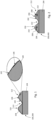
- Figure 1 shows, by means of a sectional view of a first embodiment of a contact surface of an electrically conductive contact element, a first process step according to a method according to the invention.
- the method is for surface treating an electrically conductive contact element 100.
- the contact element 100 for an electrical connector 300 is electrically conductive and comprises a base material 104.
- the base material 104 may comprise, for example, tin, nickel, silver, copper or alloys of tin, nickel, silver, copper and/or other elements.
- One side of the contact element 100 forms a metallic contact surface 102.
- the contact surface 102 comes into contact with the contact surface of the mating connector (not shown in the figures) when the connector 300 is mated to a mating connector.
- the contact surface 102 is coated on at least a partial region thereof with a lubricant 106.
- the lubricant 106 may comprise oil, grease, a paste, an acid, or another solid lubricant such as graphite, carbon nanotubes, MoS 2 , or mixtures thereof.
- the thickness of the applied lubricant may have values between 0.1 ⁇ m and 5 ⁇ m.
- the contact surface 102 of the contact element 100 may have a surface texture 112 of elevations 124 and recesses 122. These elevations 124 and recesses 122 may be formed periodically alternating at least in sections. In this regard, the recesses 122 form trenches and the elevations 124 form walls between them. The elevations may be in the order of 0.1 ⁇ m to 2 ⁇ m, by way of example. However, it is by no means necessary for the method according to the invention that the surface texture 112 comprises elevations 124 and recesses 122. It is understood that the contact surface 102 may have any surface texture 112, such as smooth or with other roughness.
- Figure 2 shows another embodiment of a contact surface 102 of an electrically conductive contact element 200 in a first process step according to a method according to the invention.
- the contact element 200 for an electrical connector 400 is electrically conductive and comprises a base material 204.
- the base material 204 may comprise, for example, tin, nickel, silver, copper or alloys of tin, nickel, silver, copper and/or other elements.
- One side of the contact element 200 forms a metallic contact surface 202, and the contact surface 202 comes into contact with the contact surface of the mating connector when the connector 400 is mated with a mating connector.
- caverns 208 are enclosed under the contact surface 202 and are filled with an auxiliary material 210.
- the caverns 208 are spaced apart from each other at regular intervals under the contact surface 202.
- the surface texture 212 has exemplary elevations 224 and recesses 222. These elevations 224 and recesses 222 may be formed periodically alternating, at least in sections. In this regard, the recesses 222 form trenches and the elevations 224 form walls between them.
- the elevations can be in the order of 0.1 ⁇ m to 2 ⁇ m, by way of example.
- the caverns 208 may also be irregularly spaced from one another and at varying depths under the contact surface 202. Furthermore, it is also possible for the caverns 208 to be enclosed under the contact surface 202 if the contact surface 202 does not have elevations 224 and recesses 222. For the method according to the invention, it is not necessary that the surface texture 212 comprises elevations 224 and recesses 222. It is understood that the contact surface 202 may have any surface texture 212, such as smooth or with other roughness.
- the auxiliary material 210 enclosed in the caverns 208 may comprise, for example, oil, grease, a paste, or another solid lubricant such as graphite, carbon nanotubes, MoS 2 , or mixtures thereof.
- the contact surface 202 is coated with a lubricant 206 on at least a partial region thereof.
- the lubricant 206 may comprise oil, grease, a paste, an acid, or another solid lubricant such as graphite, carbon nanotubes, MoS 2 , or mixtures thereof.
- the thickness of the applied lubricant may have values between 0.1 ⁇ m and 5 ⁇ m.
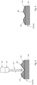
- Figure 3 shows the contact element 100 according to a first embodiment in a further process step of the method according to the invention.
- the figure shows a schematic representation of the surface treatment of the contact element 100 using plasma.
- a plasma generator 118 for controlling and monitoring the plasma system, is shown schematically with a plasma nozzle 114 directed at the material to be treated.
- the directed plasma nozzle 114 is used to generate and propagate the plasma.
- Various nozzle systems such as single nozzles or rotating nozzles, can be used as plasma sources.
- a plasma flame 116 is used to treat the contact surface 102.
- the distance d of the plasma nozzle 114 to the contact surface 102 is in the range of 5 mm to 100 mm.
- the plasma flame 116 in a pressure range of 1 mbar to 8 bar, thus, for example, treatment of surfaces can also be carried out at atmospheric pressure.
- the power of the plasma flame 116 is in a range of 50 W to 5 kW.
- the treatment of the contact surface 102 is part of a continuous process in which the contact element 100 passes through the plasma flame 116 at a speed of 100 mm/s or 200 mm/s, for example.
- the dwell time of the contact surface 102 under the plasma flame 116 is then between 5 ms and 500 ms.
- Figure 4 shows an exemplary first embodiment of a contact surface 102 of an electrically conductive contact element 100 after surface treatment with plasma.
- the plasma treatment has produced a coating 120 of a solid lubricant, preferably carbon, on at least a partial region of the contact surface 102.
- This coating 120 of a solid lubricant may have a thickness of 1 nm to 300 nm and may be transparent. At least part of the applied lubricant from the previous process step thus has been at least partially converted into a coating of a solid lubricant preferably consisting of carbon.
- the surface properties of the contact element can be improved by the plasma treatment. Accordingly, the treatment reduces unevenness in the contact surface, thus achieving a lower square roughness.
- a higher hardness of the coated surface can additionally be achieved.
- the hardness of the connector surface can be determined by means of nanoidentification.
- An indenter with a known geometry is pressed into the surface to be tested with a defined force curve. When the specified maximum force is reached, the indenter is released again in a controlled manner. The indentation depth is recorded both during loading and unloading.
- Various parameters can be calculated from the applied force, the shape of the indenter and the indentation depth.
- For a measurement of the surface hardness at least two measuring points are approached at a predefined distance. The mean value of all measuring points on a surface can be used as a comparable measure of surface hardness. The measurement is first performed on an untreated surface and then a second time after plasma treatment.
- an exemplary average hardness value of 450 N/mm 2 can be determined for the untreated surface.
- an exemplary mean value of 750 N/mm 2 can be determined for a textured and plasma-treated surface.
- surfaces exhibit a higher hardness after plasma treatment.
- an increase in hardness of 40% to 80% can be observed in particular for contact surfaces textured before plasma treatment compared to untreated surfaces.
- a spatially resolved characterization of the plasma-treated surface in terms of roughness, hardness and chemical composition can advantageously reveal a significantly more uniform image than contacts that have been stamped or electroplated, for example.
- the plasma flame can be generated in a low-pressure plasma chamber under vacuum.
- Reference number Description 100 200 Contact element 102, 202 Contact surface 104, 204 Basic material 106, 206 Lubricant 208 Cavern 210 Auxiliary material 112, 212 Surface texture 114 Plasma nozzle 116 Plasma flame 118 Plasma generator 120 Coating from a solid lubricant 122, 222 Recess 124, 224 Elevation d Distance of the plasma nozzle to the contact surface 300, 400 Connector
Landscapes
- Chemical & Material Sciences (AREA)
- Engineering & Computer Science (AREA)
- Manufacturing & Machinery (AREA)
- Chemical Kinetics & Catalysis (AREA)
- Materials Engineering (AREA)
- Mechanical Engineering (AREA)
- Metallurgy (AREA)
- Organic Chemistry (AREA)
- Manufacturing Of Electrical Connectors (AREA)
- Manufacture Of Switches (AREA)
Abstract
Description
- The present invention relates to a method for surface treatment of an electrically conductive contact element for an electrical connector. Furthermore, the invention relates to an electrically conductive contact element whose surface is treated by means of such a method.
- Electrical connectors and their contact elements are known in numerous designs. Electrical connectors are intended to be mated with a suitable mating connector to establish an electrical connection. Electrical connectors are generally used either for signal transmission or for power transmission. For this purpose, electrical connectors generally have electrically conductive contact elements that come into contact with a contact element of the mating connector when the connector is mated. Frequently, the contact elements of one connector element are designed as contact pins and those of the mating connector as contact springs. When the connector and mating connector are mated, the contact springs exert elastic spring forces on the contact pins to ensure a reliable electrically conductive connection.
- Electrical connectors are used in motor vehicles, for example, to transmit power and network electrical and electronic systems. In motor vehicles, connectors are exposed to strong temperature fluctuations, vibrations, moisture and corrosive media. An increase in operating temperatures results in increased wear, particularly in the case of the widely used tin-plated copper-based contact elements.
- In particular, base metal contact surfaces, e.g. with tin, nickel or their alloys, have a tendency to fretting corrosion ("fretting" or "scuffing") in the event of small relative movements. Furthermore, in the case of high-pole connectors, the mating forces are often outside the required forces, especially during initial mating, and in the case of noble contact surfaces, e.g. noble metal-based, the tendency to cold welding represents a known problem.
- In addition to high wear resistance, low mating and drawing forces are therefore required to facilitate the assembly and maintenance of connectors. To increase occupational safety, the specified mating force must not exceed certain limits, especially during initial mating.
- In addition, partial abrasion takes place on the contact surface of a contact element during mating of a connector with a mating connector. This wear caused by abrasion limits the mating frequency of connectors and thus reduces their operating times.
- The German patent specification
DE 10 2016 214 693 B4 describes an electrical contact element of a connector in which caverns filled with an auxiliary material are arranged under the contact surface. The contact surface was previously textured by laser irradiation. After the connector has been mated for the first time into a mating connector, the caverns break open causing the auxiliary material to escape and to cover the contact surface with a lubricating film. This lubricating film results in reduced mating force when the connector is mated again. The treatment of a surface with an interference pattern from laser radiation, in which exemplarily a dimpled structure is created, is referred to below as a textured surface. - However, assembly boundary conditions also define standards for the mating force when the connector is first mated with a mating connector. This initial mating force is of particular importance when assembling connectors with a high number of contacts. There is an additional requirement for the contact surface of the connector to be heat-resistant, as the connectors can also be further processed in warm regions. Applying a lubricating film to the contact surface of the connector is therefore not a suitable solution, as the lubricating film would evaporate at warm temperatures.
- Therefore, there is a need for a cost-effective and reliable process that treats the contact surface of an electrical connector in such a way that the initial mating force can be reduced when mating with a mating connector, and the surface treatment does not lose its effect even under adverse environmental conditions.
- This task is solved by the subject-matter of the independent claims. Advantageous embodiments of the present invention are the subject matter of the dependent claims.
- In this context, the present invention is based on the idea that improved surface properties of the contact surface of the electrical connector are achieved by treatment with plasma. For this purpose, a lubricant is first applied to the contact surface so that a coating of a solid lubricant is produced on the contact surface by the plasma treatment.
- In particular, the present invention comprises a method for surface treatment of an electrically conductive contact element for an electrical connector, wherein the electrically conductive contact element has a metallic contact surface. In addition, a lubricant is applied to at least a partial region of the contact surface of the electrically conductive contact element. Furthermore, the contact surface of the electrically conductive contact element is changed by means of plasma treatment, whereby a coating of a solid lubricant is produced at least in sections on at least a partial region of the contact surface of the electrically conductive contact element.
- The coating of a solid lubricant can be, for example, carbon, carbonaceous, or sulfide-based. A carbon layer is understood to be a thin layer consisting predominantly of the chemical element carbon. This includes, for example, graphite layers or diamond-like carbon layers. The applied lubricant layer, which serves as the initial lubricant layer, can be, for example, an oil, grease, paste, or another solid lubricant such as graphite, carbon nanotubes, MoS2 or mixtures thereof, which is modified by the plasma treatment.
- The surface treatment can reduce the roughness of the contact surface of the electrical connector and achieve a higher homogeneity. In addition, the hardness of the contact surface can be increased, e.g. by selectively creating intermetallic phases IMPs or a nanocrystalline microstructure. Each of these improved properties, independent of the others, reduces the initial mating force when mating the connector with a mating connector. In addition, the variations in the coefficient of friction over the entire contact surface can be reduced.
- According to an advantageous further development of the present invention, the contact surface of the electrically conductive contact element has a surface texture consisting of elevations and recesses, so that the lubricant applied to the contact surface adheres particularly well.
- The plasma is excited in a pressure range from 1 mbar to 8 bar, which means that, advantageously, no vacuum chamber is required for the plasma treatment, which can instead be carried out using atmospheric pressure plasma. This has the advantage that liquid chemicals can be dispensed with entirely. For this purpose, non-hazardous gases such as nitrogen or compressed air can be used for plasma generation. Alternatively, the plasma can be excited under low vacuum or slight overpressure.
- In the following, a plasma is understood to be partially or completely ionized gas. The cold or hot plasma is generated and spread by a plasma nozzle directed at the material. Inside the nozzle, the plasma is generated by high voltage between a stator and a rotor. Through an arc-like high-voltage discharge, the ionized gas is directed onto the surface to be treated. For example, hydrogen, argon, nitrogen or compressed air can be used as the gas to be ionized.
- Advantageously, the power of the plasma is in the range of 50 W to 5 kW to produce the previously mentioned coating of a solid lubricant from the applied lubricant layer.
- According to an advantageous further development of the present invention, caverns filled with an auxiliary material are enclosed under the contact surface of the electrically conductive contact element. These filled caverns break open in the course of the first mating of the connector with a mating connector, allowing the auxiliary material to escape and develop its effect. This allows the mating force to be reduced in the first mating process and even more so for all subsequent mating processes.
- An auxiliary material, also called an additive, is a substance that is added in rather small quantities to achieve or improve certain properties.
- A cavern is understood to be an artificially created cavity below the surface. The arrangement of the caverns below the contact surface means that the caverns do not have an outlet at the contact surface or, at most, an outlet of such narrow dimensions that auxiliary material filled into the caverns cannot be reached without creating a breakthrough from the contact surface into the cavern.
- According to another advantageous embodiment of the present invention, the auxiliary material is selected from the group consisting of antioxidants, corrosion inhibitors, lubricants, another solid lubricant, and acids. This group of substances facilitates, after leakage to the contact surface of a connector, the mating of this connector with a mating connector.
- According to an advantageous further development of the present invention, the plasma treatment of the electrically conductive contact element is part of a continuous process. This has the advantage that the edges of the contact surface are also treated uniformly. As a result, a uniformly thin layer of a solid lubricant can advantageously be obtained, as a result of which the contact surface has a high degree of homogeneity.
- According to an advantageous further development of the present invention, the plasma treatment comprises irradiation with a plasma flame, wherein the dwell time of the electrically conductive contact element in the plasma flame is between 5 ms and 500 ms. The positive effects mentioned above already occur after this short dwell time, whereby high numbers of pieces can be treated in a short time.
- According to an advantageous further development of the present invention, the plasma flame exits from a plasma nozzle, with the distance of the contact surface to the plasma nozzle being 5 mm to 100 mm. This targeted plasma treatment allows an easy integration into an existing manufacturing facility and compliance with safety regulations without the need for additional shielding precautions.
- According to an advantageous further development of the present invention, the coating of a solid lubricant produced by the plasma treatment has a thickness of 1 nm to 300 nm. This thin coating allows the plasma treatment to be used for a wide variety of connector types, which can be mated with a matching mating connector without having to adjust the dimensions.
- According to an advantageous further development of the present invention, the thickness of the lubricant applied to the contact surface of the electrically conductive contact element is between 0.1 µm and 5 µm. The thinly applied layer adheres particularly well to the rough metallic contact surface.
- The present invention further relates to an associated electrically conductive contact element for an electrical connector, which has a metallic contact surface. In addition, the contact surface has, at least in sections, a coating of a solid lubricant produced from a lubricant layer by treatment with plasma. This electrically conductive contact element has the advantage of having a lower first mating force from the start than conventional contact elements. In addition, the standard deviation of the coefficient of friction is reduced, which is particularly important for connectors with a high number of contacts.
- It is also advantageous if caverns filled with an auxiliary material are enclosed under the contact surface of the electrically conductive contact element. These break open when the contact element first makes contact with a mating contact, the auxiliary material escapes and the mating force can be reduced during the first mating process and even more so for all subsequent mating processes. Due to the fact that the filled caverns are located under the contact surface, negative effects such as gumming can be avoided. In addition, undesirable losses of the auxiliary material due to the solid embedding are excluded.
- According to another advantageous embodiment of an electrically conductive contact element, the auxiliary material is selected from the group of antioxidants, corrosion inhibitors, lubricants, another solid lubricant and acids. These substances reduce wear caused by abrasion, which can increase the mating frequency of the connectors.
- According to a further advantageous embodiment of an electrically conductive contact element, the metallic contact surface comprises tin, and/or nickel, and/or silver, and/or copper and/or alloys of tin, nickel, silver, copper. These materials are rust and heat resistant whereby a longevity of the connector can be guaranteed.
- According to an advantageous further development of the present invention, a square roughness of the surface in the mating direction is less than 0.3 µm. This value is below the measured values for surfaces, which have not been modified by means of plasma treatment according to the invention. Thus, advantageously, a lower roughness could be achieved, resulting in a more uniform surface and thus an improved mating of the connector with the mating connector.
- Surface roughness is the degree of unevenness of a solid surface below its shape or waviness, but above the irregularity of crystal lattice structures. Roughness can affect material properties such as friction. One of the roughness characteristics is the square roughness. This can be detected by optical measurement methods. The evaluation of the measurements was based on the DIN EN ISO 4287 and DIN EN ISO 11562 series of standards. For mating a connector with a mating connector, the roughness in the mating direction is of particular importance. Therefore, in the present case, the measurement is aligned to the mating direction. In one embodiment, this alignment can be made along the surface texture. If the surface texture has elevations and recesses, as in the above-mentioned embodiment, the alignment of the measurement takes place along the elevations and recesses.
- For a better understanding of the present invention, it will be explained in more detail with reference to the examples of embodiments shown in the following figures. In this context, identical parts are provided with identical reference signs and identical component designations. Furthermore, some features or combinations of features from the different embodiments shown and described may also represent independent, inventive solutions or solutions according to the invention. Showing:
- Fig. 1
- a schematic sectional view of a contact surface in a first embodiment in a process step according to a method according to the invention, including an enlarged section of the contact surface;
- Fig. 2
- a schematic sectional view of a contact surface in a further embodiment in a process step according to a method according to the invention;
- Fig. 3
- a schematic representation of the surface treatment of a first embodiment of the contact surface by means of plasma in a further process step;
- Fig. 4
- a schematic sectional view of the contact surface of a first embodiment of the contact surface after plasma treatment in a further process step.
-
Figure 1 shows, by means of a sectional view of a first embodiment of a contact surface of an electrically conductive contact element, a first process step according to a method according to the invention. - The method is for surface treating an electrically conductive contact element 100. The contact element 100 for an electrical connector 300 is electrically conductive and comprises a
base material 104. Thebase material 104 may comprise, for example, tin, nickel, silver, copper or alloys of tin, nickel, silver, copper and/or other elements. One side of the contact element 100 forms ametallic contact surface 102. Thecontact surface 102 comes into contact with the contact surface of the mating connector (not shown in the figures) when the connector 300 is mated to a mating connector. - The
contact surface 102 is coated on at least a partial region thereof with alubricant 106. For example, thelubricant 106 may comprise oil, grease, a paste, an acid, or another solid lubricant such as graphite, carbon nanotubes, MoS2, or mixtures thereof. The thickness of the applied lubricant may have values between 0.1 µm and 5 µm. - In an advantageous embodiment, the
contact surface 102 of the contact element 100 may have asurface texture 112 ofelevations 124 and recesses 122. Theseelevations 124 and recesses 122 may be formed periodically alternating at least in sections. In this regard, therecesses 122 form trenches and theelevations 124 form walls between them. The elevations may be in the order of 0.1 µm to 2 µm, by way of example. However, it is by no means necessary for the method according to the invention that thesurface texture 112 compriseselevations 124 and recesses 122. It is understood that thecontact surface 102 may have anysurface texture 112, such as smooth or with other roughness. -
Figure 2 shows another embodiment of acontact surface 102 of an electrically conductive contact element 200 in a first process step according to a method according to the invention. - The contact element 200 for an electrical connector 400 is electrically conductive and comprises a
base material 204. Thebase material 204 may comprise, for example, tin, nickel, silver, copper or alloys of tin, nickel, silver, copper and/or other elements. One side of the contact element 200 forms ametallic contact surface 202, and thecontact surface 202 comes into contact with the contact surface of the mating connector when the connector 400 is mated with a mating connector. - In the embodiment shown,
caverns 208 are enclosed under thecontact surface 202 and are filled with anauxiliary material 210. In the embodiment shown, thecaverns 208 are spaced apart from each other at regular intervals under thecontact surface 202. In this embodiment, thesurface texture 212 hasexemplary elevations 224 and recesses 222. Theseelevations 224 and recesses 222 may be formed periodically alternating, at least in sections. In this regard, therecesses 222 form trenches and theelevations 224 form walls between them. The elevations can be in the order of 0.1 µm to 2 µm, by way of example. - It is understood that the
caverns 208 may also be irregularly spaced from one another and at varying depths under thecontact surface 202. Furthermore, it is also possible for thecaverns 208 to be enclosed under thecontact surface 202 if thecontact surface 202 does not haveelevations 224 and recesses 222. For the method according to the invention, it is not necessary that thesurface texture 212 compriseselevations 224 and recesses 222. It is understood that thecontact surface 202 may have anysurface texture 212, such as smooth or with other roughness. - The
auxiliary material 210 enclosed in thecaverns 208 may comprise, for example, oil, grease, a paste, or another solid lubricant such as graphite, carbon nanotubes, MoS2 , or mixtures thereof. Thecontact surface 202 is coated with alubricant 206 on at least a partial region thereof. For example, thelubricant 206 may comprise oil, grease, a paste, an acid, or another solid lubricant such as graphite, carbon nanotubes, MoS2 , or mixtures thereof. The thickness of the applied lubricant may have values between 0.1 µm and 5 µm. -
Figure 3 shows the contact element 100 according to a first embodiment in a further process step of the method according to the invention. - The figure shows a schematic representation of the surface treatment of the contact element 100 using plasma. In one possible embodiment, a
plasma generator 118, for controlling and monitoring the plasma system, is shown schematically with aplasma nozzle 114 directed at the material to be treated. The directedplasma nozzle 114 is used to generate and propagate the plasma. Various nozzle systems, such as single nozzles or rotating nozzles, can be used as plasma sources. From theplasma nozzle 114, aplasma flame 116 is used to treat thecontact surface 102. The distance d of theplasma nozzle 114 to thecontact surface 102 is in the range of 5 mm to 100 mm. - In this process, it is possible to generate the
plasma flame 116 in a pressure range of 1 mbar to 8 bar, thus, for example, treatment of surfaces can also be carried out at atmospheric pressure. The power of theplasma flame 116 is in a range of 50 W to 5 kW. In this case, the treatment of thecontact surface 102 is part of a continuous process in which the contact element 100 passes through theplasma flame 116 at a speed of 100 mm/s or 200 mm/s, for example. The dwell time of thecontact surface 102 under theplasma flame 116 is then between 5 ms and 500 ms. - It is clear, however, that the values given are only given by way of example and are intended to aid understanding, but in no way limit the invention to these values. Both the passage speed, the distance, and the dwell time can be adjusted as desired and can be adapted to different values of the power of the plasma flame.
-
Figure 4 shows an exemplary first embodiment of acontact surface 102 of an electrically conductive contact element 100 after surface treatment with plasma. The plasma treatment has produced acoating 120 of a solid lubricant, preferably carbon, on at least a partial region of thecontact surface 102. Thiscoating 120 of a solid lubricant may have a thickness of 1 nm to 300 nm and may be transparent. At least part of the applied lubricant from the previous process step thus has been at least partially converted into a coating of a solid lubricant preferably consisting of carbon. - In a second embodiment (not shown), it is quite possible to likewise create a
coating 120 of a solid lubricant on thecontact surface 202 if, as in a previously mentioned second embodiment of the previous process step, caverns filled with an auxiliary material are enclosed under thecontact surface 102. The caverns remain unchanged by the plasma treatment. - Advantageously, in addition to the preferably carbon or carbon-containing coating, the surface properties of the contact element can be improved by the plasma treatment. Accordingly, the treatment reduces unevenness in the contact surface, thus achieving a lower square roughness.
- Experimental investigations have shown that the square roughness of a surface after treatment with plasma is less than 0.3 µm. This value is 0.1 µm lower than the value of the square roughness for a surface not treated by means of the process according to the invention.
- Advantageously, a higher hardness of the coated surface can additionally be achieved. The hardness of the connector surface can be determined by means of nanoidentification. An indenter with a known geometry is pressed into the surface to be tested with a defined force curve. When the specified maximum force is reached, the indenter is released again in a controlled manner. The indentation depth is recorded both during loading and unloading. Various parameters can be calculated from the applied force, the shape of the indenter and the indentation depth. For a measurement of the surface hardness, at least two measuring points are approached at a predefined distance. The mean value of all measuring points on a surface can be used as a comparable measure of surface hardness. The measurement is first performed on an untreated surface and then a second time after plasma treatment. In an exemplary measurement with 51 measuring points at a distance of 100 µm, an exemplary average hardness value of 450 N/mm2 can be determined for the untreated surface. However, for a textured and plasma-treated surface, an exemplary mean value of 750 N/mm2 can be determined.
- Thus, surfaces exhibit a higher hardness after plasma treatment. When comparing the mean values, an increase in hardness of 40% to 80% can be observed in particular for contact surfaces textured before plasma treatment compared to untreated surfaces.
- Finally, a spatially resolved characterization of the plasma-treated surface in terms of roughness, hardness and chemical composition can advantageously reveal a significantly more uniform image than contacts that have been stamped or electroplated, for example.
- These advantageous properties occur independently of each other and lead independently of each other to a smaller variation of the coefficient of friction. Within a surface, a narrower distribution of the standard deviation of the coefficient of friction can thus be demonstrated by means of the method according to the invention.
- It should be noted that it is quite possible to achieve the same advantageous properties using a different plasma generation method. For example, the plasma flame can be generated in a low-pressure plasma chamber under vacuum.
List of reference signs: Reference number Description 100, 200 Contact element 102, 202 Contact surface 104, 204 Basic material 106, 206 Lubricant 208 Cavern 210 Auxiliary material 112, 212 Surface texture 114 Plasma nozzle 116 Plasma flame 118 Plasma generator 120 Coating from a solid lubricant 122, 222 Recess 124, 224 Elevation d Distance of the plasma nozzle to the contact surface 300, 400 Connector
Claims (16)
- A method for surface treating an electrically conductive contact element (100, 200) for an electrical connector (300, 400),wherein the electrically conductive contact element (100, 200) comprises a metallic contact surface (102, 202), andwherein a lubricant (106, 206) is applied to at least a partial region of the contact surface (102, 202) of the electrically conductive contact element (100, 200), andwherein the contact surface (102, 202) of the electrically conductive contact element (100, 200) is changed by means of plasma treatment, whereby a coating (120) of a solid lubricant is produced at least in sections on at least a partial region of the contact surface (102, 202) of the electrically conductive contact element (100, 200).
- The method according to claim 1,
wherein the contact surface (102, 202) of the electrically conductive contact element (100, 200) has a surface texture of elevations (124, 224) and recesses (122, 222). - The method according to any one of the preceding claims,
wherein the plasma is excited in a pressure range from 1 mbar to 8 bar. - The method according to any one of the preceding claims,
wherein the power of the plasma is in the range of 50 W to 5 kW. - The method according to any one of the preceding claims,
wherein caverns (208) filled with an auxiliary material (210) are enclosed under the contact surface (102, 202) of the electrically conductive contact element (100, 200). - The method according to any one of the preceding claims,
wherein the auxiliary material (210) is selected from the group consisting of antioxidants, corrosion inhibitors, lubricants, another solid lubricant, and acids. - The method according to any one of the preceding claims,
wherein the plasma treatment of the electrically conductive contact element (100, 200) is part of a continuous process. - The method according to any one of the preceding claims,wherein the plasma treatment comprises irradiation with a plasma flame (116), andwherein the dwell time of the electrically conductive contact element (100, 200) in the plasma flame (116) is between 5 ms and 500 ms.
- The method of claim 8,wherein the plasma flame (116) exits from a plasma nozzle (114), andwherein the distance of the contact surface to the plasma nozzle (114) is 5 mm to 100 mm.
- The method according to any one of the preceding claims,
wherein the coating (120) of a solid lubricant produced by the plasma treatment has a thickness of 1 nm to 300 nm. - The method according to any one of the preceding claims,
wherein the thickness of the lubricant (106, 206) applied to the contact surface (102, 202) of the electrically conductive contact element (100, 200) is between 0.1 µm and 5 µm. - Electrically conductive contact element (100, 200) for an electrical connector (300, 400),which has a metallic contact surface (102, 202),wherein the contact surface (102, 202) has, at least in sections, a coating (120) of a solid lubricant produced by treatment with plasma from a lubricant layer (106, 206).
- An electrically conductive contact element (100, 200) according to claim 12,
wherein caverns (208) filled with an auxiliary material (210) are enclosed below the contact surface (102, 202). - An electrically conductive contact element (100, 200) according to any one of claims 12 or 13,
wherein said auxiliary material (210) is selected from the group consisting of antioxidants, corrosion inhibitors, lubricants, another solid lubricant, and acids. - An electrically conductive contact element (100, 200) according to any one of claims 12 to 14,
wherein the metallic contact surface (102, 202) comprises tin, and/or nickel, and/or silver, and/or copper, and/or alloys of tin, nickel, silver, copper. - An electrically conductive contact element (100, 200) according to any one of claims 12 to 15,
wherein a square roughness of the surface in the mating direction is less than 0.3 µm.
Applications Claiming Priority (1)
| Application Number | Priority Date | Filing Date | Title |
|---|---|---|---|
| DE102021130188.2A DE102021130188A1 (en) | 2021-11-18 | 2021-11-18 | METHOD OF SURFACE TREATMENT OF AN ELECTRICAL CONTACT ELEMENT AND CONTACT ELEMENT |
Publications (1)
| Publication Number | Publication Date |
|---|---|
| EP4183894A1 true EP4183894A1 (en) | 2023-05-24 |
Family
ID=84358664
Family Applications (1)
| Application Number | Title | Priority Date | Filing Date |
|---|---|---|---|
| EP22208081.4A Pending EP4183894A1 (en) | 2021-11-18 | 2022-11-17 | Method for surface treatment of an electrical contact element and contact element |
Country Status (6)
| Country | Link |
|---|---|
| US (1) | US20230155310A1 (en) |
| EP (1) | EP4183894A1 (en) |
| JP (1) | JP7694869B2 (en) |
| KR (1) | KR102871356B1 (en) |
| CN (1) | CN116136021B (en) |
| DE (1) | DE102021130188A1 (en) |
Families Citing this family (1)
| Publication number | Priority date | Publication date | Assignee | Title |
|---|---|---|---|---|
| DE102023106086A1 (en) * | 2023-03-10 | 2024-09-12 | Te Connectivity Solutions Gmbh | ELECTRICAL CONTACT ELEMENT FOR AN ELECTRICAL CONNECTOR WITH SURFACE TEXTURE AND METHOD FOR SURFACE TREATMENT OF AN ELECTRICAL CONTACT ELEMENT |
Citations (4)
| Publication number | Priority date | Publication date | Assignee | Title |
|---|---|---|---|---|
| US1654509A (en) * | 1924-08-30 | 1927-12-27 | Bound Brook Oil Less Bearing | Antifriction bearing and method of forming the same |
| US20030219622A1 (en) * | 2002-04-22 | 2003-11-27 | Niebauer Daniel A. | Electrical connectors incorporating low friction coatings and methods for making them |
| US20140102594A1 (en) * | 2009-07-20 | 2014-04-17 | Ontos Equipment Systems, Inc. | Method of plasma preparation of metallic contacts to enhance mechanical and electrical integrity of subsequent interconnect bonds |
| WO2018029179A1 (en) * | 2016-08-08 | 2018-02-15 | Te Connectivity Germany Gmbh | Electrical contact element for an electrical connector having microstructured caverns under the contact surface |
Family Cites Families (43)
| Publication number | Priority date | Publication date | Assignee | Title |
|---|---|---|---|---|
| US3482202A (en) * | 1967-03-15 | 1969-12-02 | Westinghouse Electric Corp | Electrical apparatus and self-lubricating contact |
| US4268568A (en) * | 1979-05-14 | 1981-05-19 | Bell Telephone Laboratories, Incorporated | Lubricated electrical contacts |
| US4320251A (en) * | 1980-07-28 | 1982-03-16 | Solamat Inc. | Ohmic contacts for solar cells by arc plasma spraying |
| HU189862B (en) | 1984-04-18 | 1986-08-28 | Villamosipari Kutato Intezet,Hu | Method for making electric contact |
| JPH0548368Y2 (en) * | 1988-09-02 | 1993-12-24 | ||
| US5368947A (en) * | 1991-08-12 | 1994-11-29 | The Penn State Research Foundation | Method of producing a slip-resistant substrate by depositing raised, bead-like configurations of a compatible material at select locations thereon, and a substrate including same |
| US6183886B1 (en) * | 1998-04-03 | 2001-02-06 | Olin Corporation | Tin coatings incorporating selected elemental additions to reduce discoloration |
| US6294261B1 (en) * | 1999-10-01 | 2001-09-25 | General Electric Company | Method for smoothing the surface of a protective coating |
| US20030176055A1 (en) * | 2000-07-24 | 2003-09-18 | United Microelectronics Corp. | Method and structure for reducing capacitance between interconnect lines |
| JP2002343168A (en) * | 2001-05-11 | 2002-11-29 | Mitsubishi Electric Corp | Sliding conductor |
| US7270890B2 (en) * | 2002-09-23 | 2007-09-18 | Siemens Power Generation, Inc. | Wear monitoring system with embedded conductors |
| US7391116B2 (en) * | 2003-10-14 | 2008-06-24 | Gbc Metals, Llc | Fretting and whisker resistant coating system and method |
| WO2005038985A2 (en) * | 2003-10-16 | 2005-04-28 | Abb Research Ltd. | COATINGS OF Mn+1AXn MATERIAL FOR ELECTRICAL CONTACT ELEMENTS |
| US20070163638A1 (en) * | 2004-02-19 | 2007-07-19 | Nanosolar, Inc. | Photovoltaic devices printed from nanostructured particles |
| US8623448B2 (en) * | 2004-02-19 | 2014-01-07 | Nanosolar, Inc. | High-throughput printing of semiconductor precursor layer from chalcogenide microflake particles |
| US20070163639A1 (en) * | 2004-02-19 | 2007-07-19 | Nanosolar, Inc. | High-throughput printing of semiconductor precursor layer from microflake particles |
| US7316850B2 (en) * | 2004-03-02 | 2008-01-08 | Honeywell International Inc. | Modified MCrAlY coatings on turbine blade tips with improved durability |
| US7278857B2 (en) * | 2006-02-02 | 2007-10-09 | Palo Alto Research Center Incorporated | Brittle fracture resistant spring |
| US20100086702A1 (en) * | 2008-10-06 | 2010-04-08 | Lincoln Global, Inc. | Methods and materials for laser cladding |
| US10157731B2 (en) * | 2008-11-12 | 2018-12-18 | Applied Materials, Inc. | Semiconductor processing apparatus with protective coating including amorphous phase |
| US20100124616A1 (en) * | 2008-11-19 | 2010-05-20 | General Electric Company | Method of forming an abradable coating |
| JP2012057212A (en) * | 2010-09-08 | 2012-03-22 | Furukawa Electric Co Ltd:The | Composite plated material, and electric component and electronic component using the same |
| DE102011078546A1 (en) * | 2011-07-01 | 2013-01-03 | Tyco Electronics Amp Gmbh | Electrical contact coating |
| DE102011088793A1 (en) * | 2011-12-16 | 2013-06-20 | Tyco Electronics Amp Gmbh | Electrical connector with microstructured contact element |
| US20150079370A1 (en) * | 2013-09-18 | 2015-03-19 | Applied Materials, Inc. | Coating architecture for plasma sprayed chamber components |
| DE102014017886A1 (en) * | 2014-12-04 | 2016-06-09 | Auto-Kabel Management Gmbh | Method for producing an electrical connection part |
| WO2018024778A1 (en) * | 2016-08-03 | 2018-02-08 | Evonik Oil Additives Gmbh | Method for the preparation of ceramic coatings on electrically conductive substrates |
| JP2018056119A (en) | 2016-09-21 | 2018-04-05 | 矢崎総業株式会社 | Electric contact, connector and manufacturing method of electric contact |
| JP6423025B2 (en) * | 2017-01-17 | 2018-11-14 | 三菱伸銅株式会社 | Tin-plated copper terminal material excellent in insertion / removability and manufacturing method thereof |
| JP6965595B2 (en) * | 2017-06-23 | 2021-11-10 | 住友電気工業株式会社 | Electric wire with terminal and its manufacturing method |
| JP7040224B2 (en) * | 2018-03-30 | 2022-03-23 | 三菱マテリアル株式会社 | Tin-plated copper terminal material and its manufacturing method |
| DE102018005352A1 (en) * | 2018-07-05 | 2020-01-09 | Dr.-Ing. Max Schlötter GmbH & Co KG | Silver electrolyte for the deposition of dispersion silver layers and contact surfaces with dispersion silver layers |
| CN112739480B (en) * | 2018-09-20 | 2023-05-02 | 由加拿大自然资源部长代表的加拿大国王陛下 | Methods and compositions for forming hybrid aluminum-based composite coatings |
| CN110228251B (en) * | 2019-06-06 | 2021-06-04 | 沈阳航空航天大学 | A kind of high-efficiency heterogeneous joint of light alloy and composite material and preparation method thereof |
| US11133614B2 (en) * | 2019-08-30 | 2021-09-28 | TE Connectivity Services Gmbh | Low insertion force contact and method of manufacture |
| US12294185B2 (en) * | 2019-09-10 | 2025-05-06 | Ticona Llc | Electrical connector formed from a polymer composition having a low dielectric constant and dissipation factor |
| CN110643991B (en) * | 2019-09-26 | 2021-11-19 | 西安天瑞达光电技术股份有限公司 | Metal material surface treatment method |
| CN111500996B (en) * | 2020-05-15 | 2021-12-31 | 中国科学院兰州化学物理研究所 | Method for preparing gold conductive lubricating film of vacuum electric contact component by magnetron sputtering method |
| US20210310116A1 (en) * | 2021-06-17 | 2021-10-07 | Newsotech, Inc. | Asynchronous conversion of metals to metal ceramics |
| CN117977331A (en) * | 2022-10-26 | 2024-05-03 | 泰科电子(上海)有限公司 | Conductive terminal manufacturing method and conductive terminal |
| CN117996479A (en) * | 2022-10-31 | 2024-05-07 | 泰科电子(上海)有限公司 | Conductive terminal and electric connector applied by same |
| US12410375B2 (en) * | 2022-11-30 | 2025-09-09 | University Of North Texas | Coating comprising a transition metal dichalcogenide, and coated articles and methods relating thereto |
| DE102023103001A1 (en) * | 2023-02-08 | 2024-08-08 | Te Connectivity Solutions Gmbh | Self-lubricating coating, process for its manufacture and electrical contact |
-
2021
- 2021-11-18 DE DE102021130188.2A patent/DE102021130188A1/en active Pending
-
2022
- 2022-11-15 JP JP2022182311A patent/JP7694869B2/en active Active
- 2022-11-16 CN CN202211432896.1A patent/CN116136021B/en active Active
- 2022-11-16 KR KR1020220153503A patent/KR102871356B1/en active Active
- 2022-11-17 EP EP22208081.4A patent/EP4183894A1/en active Pending
- 2022-11-18 US US17/989,919 patent/US20230155310A1/en active Pending
Patent Citations (5)
| Publication number | Priority date | Publication date | Assignee | Title |
|---|---|---|---|---|
| US1654509A (en) * | 1924-08-30 | 1927-12-27 | Bound Brook Oil Less Bearing | Antifriction bearing and method of forming the same |
| US20030219622A1 (en) * | 2002-04-22 | 2003-11-27 | Niebauer Daniel A. | Electrical connectors incorporating low friction coatings and methods for making them |
| US20140102594A1 (en) * | 2009-07-20 | 2014-04-17 | Ontos Equipment Systems, Inc. | Method of plasma preparation of metallic contacts to enhance mechanical and electrical integrity of subsequent interconnect bonds |
| WO2018029179A1 (en) * | 2016-08-08 | 2018-02-15 | Te Connectivity Germany Gmbh | Electrical contact element for an electrical connector having microstructured caverns under the contact surface |
| DE102016214693B4 (en) | 2016-08-08 | 2018-05-09 | Steinbeiss-Forschungszentrum, Material Engineering Center Saarland | An electrically conductive contact element for an electrical connector, an electrical connector comprising such a contact element, and methods for enclosing an assistant under the contact surface of such a contact element |
Also Published As
| Publication number | Publication date |
|---|---|
| JP7694869B2 (en) | 2025-06-18 |
| JP2023075055A (en) | 2023-05-30 |
| CN116136021B (en) | 2025-04-15 |
| KR102871356B1 (en) | 2025-10-15 |
| KR20230073118A (en) | 2023-05-25 |
| CN116136021A (en) | 2023-05-19 |
| DE102021130188A1 (en) | 2023-05-25 |
| US20230155310A1 (en) | 2023-05-18 |
Similar Documents
| Publication | Publication Date | Title |
|---|---|---|
| US11239593B2 (en) | Electrical contact element for an electrical connector having microstructured caverns under the contact surface | |
| US20230155310A1 (en) | Method for Surface Treatment of an Electrical Contact Element and Contact Element | |
| GB2346385B (en) | Surface treated rolling bearing and manufacturing method thereof | |
| JP5433356B2 (en) | Mold and mold surface processing method | |
| Park et al. | The influence of current load on fretting of electrical contacts | |
| US4394234A (en) | Method of processing electrically conductive material by glow discharge | |
| Yasumaru et al. | Corrosion performance of DLC coatings with laser-induced graphitized periodic surface structure | |
| Li et al. | Failure analysis of contact terminals in automotive high-voltage electrical connectors under combined thermal-vibration stresses | |
| DE102019130506B4 (en) | Electromechanical component with integrated lubrication and method for producing such an electromechanical component | |
| JPS6356313B2 (en) | ||
| EP4429033A1 (en) | Electrical contact element for an electrical connector with surface texture and method of surface treatment of an electrical contact element | |
| Aizawa et al. | Dry progressive stamping of copper-alloy snaps by the plasma nitrided punches | |
| US6205643B1 (en) | Method for manufacturing an electrically conductive metallic strip | |
| Ecer et al. | Friction and wear properties of nitrided and N+-implanted 17-4 PH stainless steel | |
| KR20180131035A (en) | Plasma Nano Nitride Process and Cam Pump Members thereby | |
| Bhushan et al. | Metallurgical re-examination of wear modes I: erosive, electrical arcing and fretting | |
| GB2060711A (en) | Processing electrically conductive material by glow discharge | |
| Ihara et al. | Enhanced oxide layer formation and reduced fretting wear in Ni-based alloys through Sn/MoS₂ Particle Peening | |
| Mikosianchyk et al. | Estimation of tribotechnical characteristics and signals of acoustic emission for a friction pair of steel 30HGSA and duraluminium D16 modified by an alloy VK8 | |
| Ran et al. | Corrosion Behavior and Mechanism of Gradient‐Structured 7075 Aluminum Alloy Induced by SMAT Under Simulated Marine Conditions | |
| Tolstoguzov et al. | Ion-plasma treatment of reed switch contacts: A study by time-of-flight secondary ion mass spectrometry | |
| Hornbeck et al. | Environmentally harmless plasma thermochemical processes | |
| Braceras Izaguirre | Development of plasma based surfaces, supported by electro-tribological studies. | |
| Izaguirre | Development of plasma based surfaces, supported by electro-tribological studies | |
| Ihara et al. | Sn and Mos2 Particle Peening: Promoted Oxide Layer Formation and Reduced Fretting Wear of Ni-Based Alloys at Elevated Temperatures |
Legal Events
| Date | Code | Title | Description |
|---|---|---|---|
| PUAI | Public reference made under article 153(3) epc to a published international application that has entered the european phase |
Free format text: ORIGINAL CODE: 0009012 |
|
| STAA | Information on the status of an ep patent application or granted ep patent |
Free format text: STATUS: THE APPLICATION HAS BEEN PUBLISHED |
|
| AK | Designated contracting states |
Kind code of ref document: A1 Designated state(s): AL AT BE BG CH CY CZ DE DK EE ES FI FR GB GR HR HU IE IS IT LI LT LU LV MC ME MK MT NL NO PL PT RO RS SE SI SK SM TR |
|
| STAA | Information on the status of an ep patent application or granted ep patent |
Free format text: STATUS: REQUEST FOR EXAMINATION WAS MADE |
|
| 17P | Request for examination filed |
Effective date: 20231012 |
|
| RBV | Designated contracting states (corrected) |
Designated state(s): AL AT BE BG CH CY CZ DE DK EE ES FI FR GB GR HR HU IE IS IT LI LT LU LV MC ME MK MT NL NO PL PT RO RS SE SI SK SM TR |
|
| STAA | Information on the status of an ep patent application or granted ep patent |
Free format text: STATUS: EXAMINATION IS IN PROGRESS |
|
| 17Q | First examination report despatched |
Effective date: 20250324 |