EP4182103B1 - Process for manufacturing optical elements for telescope optics usable in space missions - Google Patents
Process for manufacturing optical elements for telescope optics usable in space missions Download PDFInfo
- Publication number
- EP4182103B1 EP4182103B1 EP21752176.4A EP21752176A EP4182103B1 EP 4182103 B1 EP4182103 B1 EP 4182103B1 EP 21752176 A EP21752176 A EP 21752176A EP 4182103 B1 EP4182103 B1 EP 4182103B1
- Authority
- EP
- European Patent Office
- Prior art keywords
- shell
- matrix
- optical
- support
- optical elements
- Prior art date
- Legal status (The legal status is an assumption and is not a legal conclusion. Google has not performed a legal analysis and makes no representation as to the accuracy of the status listed.)
- Active
Links
Images

Classifications
-
- B—PERFORMING OPERATIONS; TRANSPORTING
- B21—MECHANICAL METAL-WORKING WITHOUT ESSENTIALLY REMOVING MATERIAL; PUNCHING METAL
- B21D—WORKING OR PROCESSING OF SHEET METAL OR METAL TUBES, RODS OR PROFILES WITHOUT ESSENTIALLY REMOVING MATERIAL; PUNCHING METAL
- B21D22/00—Shaping without cutting, by stamping, spinning, or deep-drawing
- B21D22/14—Spinning
- B21D22/16—Spinning over shaping mandrels or formers
-
- B—PERFORMING OPERATIONS; TRANSPORTING
- B21—MECHANICAL METAL-WORKING WITHOUT ESSENTIALLY REMOVING MATERIAL; PUNCHING METAL
- B21D—WORKING OR PROCESSING OF SHEET METAL OR METAL TUBES, RODS OR PROFILES WITHOUT ESSENTIALLY REMOVING MATERIAL; PUNCHING METAL
- B21D53/00—Making other particular articles
- B21D53/16—Making other particular articles rings, e.g. barrel hoops
-
- B—PERFORMING OPERATIONS; TRANSPORTING
- B23—MACHINE TOOLS; METAL-WORKING NOT OTHERWISE PROVIDED FOR
- B23K—SOLDERING OR UNSOLDERING; WELDING; CLADDING OR PLATING BY SOLDERING OR WELDING; CUTTING BY APPLYING HEAT LOCALLY, e.g. FLAME CUTTING; WORKING BY LASER BEAM
- B23K31/00—Processes relevant to this subclass, specially adapted for particular articles or purposes, but not covered by any single one of main groups B23K1/00 - B23K28/00
- B23K31/02—Processes relevant to this subclass, specially adapted for particular articles or purposes, but not covered by any single one of main groups B23K1/00 - B23K28/00 relating to soldering or welding
-
- B—PERFORMING OPERATIONS; TRANSPORTING
- B23—MACHINE TOOLS; METAL-WORKING NOT OTHERWISE PROVIDED FOR
- B23P—METAL-WORKING NOT OTHERWISE PROVIDED FOR; COMBINED OPERATIONS; UNIVERSAL MACHINE TOOLS
- B23P13/00—Making metal objects by operations essentially involving machining but not covered by a single other subclass
-
- B—PERFORMING OPERATIONS; TRANSPORTING
- B23—MACHINE TOOLS; METAL-WORKING NOT OTHERWISE PROVIDED FOR
- B23P—METAL-WORKING NOT OTHERWISE PROVIDED FOR; COMBINED OPERATIONS; UNIVERSAL MACHINE TOOLS
- B23P15/00—Making specific metal objects by operations not covered by a single other subclass or a group in this subclass
- B23P15/22—Making specific metal objects by operations not covered by a single other subclass or a group in this subclass cartridges or like shells
-
- B—PERFORMING OPERATIONS; TRANSPORTING
- B24—GRINDING; POLISHING
- B24B—MACHINES, DEVICES, OR PROCESSES FOR GRINDING OR POLISHING; DRESSING OR CONDITIONING OF ABRADING SURFACES; FEEDING OF GRINDING, POLISHING, OR LAPPING AGENTS
- B24B13/00—Machines or devices designed for grinding or polishing optical surfaces on lenses or surfaces of similar shape on other work; Accessories therefor
- B24B13/015—Machines or devices designed for grinding or polishing optical surfaces on lenses or surfaces of similar shape on other work; Accessories therefor of television picture tube viewing panels, headlight reflectors or the like
-
- G—PHYSICS
- G02—OPTICS
- G02B—OPTICAL ELEMENTS, SYSTEMS OR APPARATUS
- G02B23/00—Telescopes, e.g. binoculars; Periscopes; Instruments for viewing the inside of hollow bodies; Viewfinders; Optical aiming or sighting devices
-
- G—PHYSICS
- G02—OPTICS
- G02B—OPTICAL ELEMENTS, SYSTEMS OR APPARATUS
- G02B5/00—Optical elements other than lenses
- G02B5/08—Mirrors
- G02B5/10—Mirrors with curved faces
-
- G—PHYSICS
- G21—NUCLEAR PHYSICS; NUCLEAR ENGINEERING
- G21K—HANDLING OF PARTICLES OR IONISING RADIATION NOT OTHERWISE PROVIDED FOR; IRRADIATION DEVICES; GAMMA RAY OR X-RAY MICROSCOPES
- G21K1/00—Arrangements for handling particles or ionising radiation, e.g. focusing or moderating
- G21K1/06—Arrangements for handling particles or ionising radiation, e.g. focusing or moderating using diffraction, refraction or reflection, e.g. monochromators
- G21K1/067—Arrangements for handling particles or ionising radiation, e.g. focusing or moderating using diffraction, refraction or reflection, e.g. monochromators using surface reflection, e.g. grazing incidence mirrors, gratings
-
- C—CHEMISTRY; METALLURGY
- C23—COATING METALLIC MATERIAL; COATING MATERIAL WITH METALLIC MATERIAL; CHEMICAL SURFACE TREATMENT; DIFFUSION TREATMENT OF METALLIC MATERIAL; COATING BY VACUUM EVAPORATION, BY SPUTTERING, BY ION IMPLANTATION OR BY CHEMICAL VAPOUR DEPOSITION, IN GENERAL; INHIBITING CORROSION OF METALLIC MATERIAL OR INCRUSTATION IN GENERAL
- C23C—COATING METALLIC MATERIAL; COATING MATERIAL WITH METALLIC MATERIAL; SURFACE TREATMENT OF METALLIC MATERIAL BY DIFFUSION INTO THE SURFACE, BY CHEMICAL CONVERSION OR SUBSTITUTION; COATING BY VACUUM EVAPORATION, BY SPUTTERING, BY ION IMPLANTATION OR BY CHEMICAL VAPOUR DEPOSITION, IN GENERAL
- C23C18/00—Chemical coating by decomposition of either liquid compounds or solutions of the coating forming compounds, without leaving reaction products of surface material in the coating; Contact plating
- C23C18/16—Chemical coating by decomposition of either liquid compounds or solutions of the coating forming compounds, without leaving reaction products of surface material in the coating; Contact plating by reduction or substitution, e.g. electroless plating
- C23C18/1601—Process or apparatus
- C23C18/1633—Process of electroless plating
- C23C18/1689—After-treatment
-
- C—CHEMISTRY; METALLURGY
- C23—COATING METALLIC MATERIAL; COATING MATERIAL WITH METALLIC MATERIAL; CHEMICAL SURFACE TREATMENT; DIFFUSION TREATMENT OF METALLIC MATERIAL; COATING BY VACUUM EVAPORATION, BY SPUTTERING, BY ION IMPLANTATION OR BY CHEMICAL VAPOUR DEPOSITION, IN GENERAL; INHIBITING CORROSION OF METALLIC MATERIAL OR INCRUSTATION IN GENERAL
- C23C—COATING METALLIC MATERIAL; COATING MATERIAL WITH METALLIC MATERIAL; SURFACE TREATMENT OF METALLIC MATERIAL BY DIFFUSION INTO THE SURFACE, BY CHEMICAL CONVERSION OR SUBSTITUTION; COATING BY VACUUM EVAPORATION, BY SPUTTERING, BY ION IMPLANTATION OR BY CHEMICAL VAPOUR DEPOSITION, IN GENERAL
- C23C18/00—Chemical coating by decomposition of either liquid compounds or solutions of the coating forming compounds, without leaving reaction products of surface material in the coating; Contact plating
- C23C18/16—Chemical coating by decomposition of either liquid compounds or solutions of the coating forming compounds, without leaving reaction products of surface material in the coating; Contact plating by reduction or substitution, e.g. electroless plating
- C23C18/31—Coating with metals
- C23C18/32—Coating with nickel, cobalt or mixtures thereof with phosphorus or boron
-
- G—PHYSICS
- G02—OPTICS
- G02B—OPTICAL ELEMENTS, SYSTEMS OR APPARATUS
- G02B23/00—Telescopes, e.g. binoculars; Periscopes; Instruments for viewing the inside of hollow bodies; Viewfinders; Optical aiming or sighting devices
- G02B23/02—Telescopes, e.g. binoculars; Periscopes; Instruments for viewing the inside of hollow bodies; Viewfinders; Optical aiming or sighting devices involving prisms or mirrors
-
- G—PHYSICS
- G02—OPTICS
- G02B—OPTICAL ELEMENTS, SYSTEMS OR APPARATUS
- G02B7/00—Mountings, adjusting means, or light-tight connections, for optical elements
- G02B7/18—Mountings, adjusting means, or light-tight connections, for optical elements for prisms; for mirrors
- G02B7/182—Mountings, adjusting means, or light-tight connections, for optical elements for prisms; for mirrors for mirrors
- G02B7/183—Mountings, adjusting means, or light-tight connections, for optical elements for prisms; for mirrors for mirrors specially adapted for very large mirrors, e.g. for astronomy, or solar concentrators
-
- G—PHYSICS
- G21—NUCLEAR PHYSICS; NUCLEAR ENGINEERING
- G21K—HANDLING OF PARTICLES OR IONISING RADIATION NOT OTHERWISE PROVIDED FOR; IRRADIATION DEVICES; GAMMA RAY OR X-RAY MICROSCOPES
- G21K2201/00—Arrangements for handling radiation or particles
- G21K2201/06—Arrangements for handling radiation or particles using diffractive, refractive or reflecting elements
- G21K2201/064—Arrangements for handling radiation or particles using diffractive, refractive or reflecting elements having a curved surface
-
- G—PHYSICS
- G21—NUCLEAR PHYSICS; NUCLEAR ENGINEERING
- G21K—HANDLING OF PARTICLES OR IONISING RADIATION NOT OTHERWISE PROVIDED FOR; IRRADIATION DEVICES; GAMMA RAY OR X-RAY MICROSCOPES
- G21K2201/00—Arrangements for handling radiation or particles
- G21K2201/06—Arrangements for handling radiation or particles using diffractive, refractive or reflecting elements
- G21K2201/067—Construction details
Definitions
- the present invention concerns a process for manufacturing optical elements, particularly for telescope optics usable in space missions.
- the invention is preferably, although not exclusively, applied in the manufacturing of grazing incidence optics for telescopes for X rays, which will be referred to in particular, albeit without loss of generality.
- Grazing incidence optics comprise a plurality of aspherical annular optical elements concentric to one another; for example, in the Wolter-I configuration, each element has a portion with parabolic section and a portion with hyperbolic section.
- optics especially in the case of large mirrors (for example in the order of 3 m in diameter), can be manufactured by means of a modular process, namely producing a series of modules each consisting of a plurality of segments "stacked" on and spaced from one another.
- the segments consist typically of a sheet of glass (fused silica or borofloat glass or other types of glass) or silicon wafers having dimensions in the order of 100 mm ⁇ 100 mm and thickness typically less than 1 mm.
- Complete optics can comprise up to tens of thousands of segments.
- a problem connected with this construction technique is the fact that the creation of each module and the integration of the modules to form the complete mirror are long and costly operations; the process also has limits in terms of accuracy connected with the difficulty of integrating a large number of modules while maintaining a high precision.
- An alternative technique consists in producing the mirror from a limited number of monolithic annular glass shells (for example less than two hundred for optics with external diameter of 3m).
- glass shells are costly and fragile, and entail long procurement times.
- the minimum thickness of these shells is limited by the safety factors necessary for fragile materials in the work processes and not by the mechanical strength of the material.
- surface treatments on the outer surface are necessary to increase mechanical strength.
- Optical elements are also produced from a single metallic piece obtained by means of casting and machining to remove material until obtaining a thin shaped substrate. Also this technique has significant drawbacks: production difficulties with thin substrates, high cost of the initial single piece obtained by casting, long working times, very limited possibility of checking uniformity of the material until the end of the work process, non-uniform residual stress in the material, and risks of breakage during work.
- a very widespread technique for producing mirrors in one piece is replication by means of nickel electroforming starting from a metallic mandrel having negative profile of the mirror to be produced.
- this approach has some contra-indications such as: i) difficulty of producing mirrors with large diameter, limited above all by the difficulty of producing large-size mandrels with optical grade lapped surface (the largest diameter mirror produced so far with this method is 70 cm diameter); ii) the high density of the nickel, which is a drawback for producing instruments for flying in space; iii) the difficulty of obtaining very high angular resolutions with the replication technique.
- the object of the present invention is to make available an alternative process for the manufacture of optical elements, which solves the problems connected with the known methods described above.
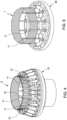
- an optical element 1 ( figure 9 ) is produced starting from a circular metal sheet 2 ( fig. 1 ).
- the material is preferably an aluminium alloy, for example aluminium alloys with magnesium (0.4 - 1.7%), manganese (0.5 - 1%) and silicon (1 - 50) like Anticorodal.
- the thickness of the sheet ranges from 0.5 to 15 mm and is preferably approximately 2 mm.
- the sheet 2 initially undergoes a step known as metal spinning, in which the sheet 2 is axially blocked between a shaped matrix 3, defining the shape to be obtained, mounted on the mandrel of a lathe (not illustrated), and a counter-head 4.
- a step known as metal spinning in which the sheet 2 is axially blocked between a shaped matrix 3, defining the shape to be obtained, mounted on the mandrel of a lathe (not illustrated), and a counter-head 4.
- the matrix 3, the counter-head 4 and the sheet 2 are coaxial to one another.
- the mandrel is made to rotate and consequently rotates the matrix 3/sheet 2/counter-head 4 assembly.
- the sheet 2 is deformed by means of a tool 5 which acts on the face of the sheet opposite the matrix 3 and is moved parallel to a generatrix of said matrix, so as to deform the sheet 2 and cause it to adhere progressively to an outer surface 6 of the matrix 3, reproducing the shape thereof.
- a central portion 7 of the sheet 2, and if necessary an outer edge opposite thereto, are removed by means of any known cutting process, thus obtaining a semi-finished product 8 in the form of an axialsymmetric shell (below, for the sake of brevity, "shell 8"), similar to that of the optical element to be obtained ( fig. 3 ).
- the shell 8 is then mounted inside a support 10 ( fig. 4 ), preferably with vertical axis, which blocks it axially and radially so as to induce the minimum possible level of stress and, therefore, internal tensions in the material.
- the support can be provided with a plurality of support ribs 11 extending along equally spaced external generatrices of the shell 8.
- the ribs 11 can be fixed to the shell, for example by means of gluing or welding, prior to removing the shell 8 from the matrix 3; the ribs 11 can therefore constitute positioning and fixing elements in the support 10, provided with fixing elements 12 cooperating with the ribs 11.
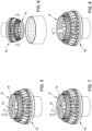
- the shell 8 undergoes a series of successive steps of the process ( figures 5-8 ) until the finished optical element 1 is produced ( fig. 9 ).
- the shell 8 undergoes a diamond turning step (precision turning by means of a diamond tool 13).
- the support 10 is mounted on a mandrel with vertical axis, not illustrated, and rotated.
- the diamond tool 13 is brought into contact with an optical surface 14 (in the example illustrated the internal surface) of the shell 8, which is machined at very high precision.
- the optical surface 14 of the shell is coated with electroless nickel (nickel phosphorous alloy, for example Kanigen ® ) by means of a deposition process by immersion in an autocatalytic chemical bath in aqueous solution.
- electroless nickel nickel phosphorous alloy, for example Kanigen ®
- a coating layer is obtained ranging from 10 to 100 um, and preferably equal to approximately 20 um.
- the immersion in the bath is preferably carried out without removing the shell 8 from the support 10, which can be overturned prior to immersion. In this way the shell is not subject to undesired tension.
- the shell 8 can be removed from the support 10 and mounted on another dedicated support for immersion in the bath.
- the shell 8 can undergo a second diamond turning step (optional) - figure 7 - in which any deformations induced by the nickel plating can be corrected and the design geometry is restored to the optical surface 14.
- the optical surface 14 can undergo a final step (optional) of grinding the azimuthal surfaces with precision milling, moderation of the profile by means of bonnet polishing and superpolishing with pitch pads or other abrasive materials to obtain a finished optical element 1 with a microroughness of the optical surface 14 less than fractions of a nanometre.
- the optical element 1 is assembled on an integration support 20 ( figure 9 ), expediently composed of a circular structure on which the different shells forming the optics are coaxially fixed by means of fixing equipment 21 which can cooperate with the ribs 11 of the shell 8, if present.
- the integration support 20 is expediently made of the same material as the shells 8, for example aluminium, so as to produce optics which are free from thermally induced tensions, mechanically stable and lightweight.
- the process is then repeated to produce other optical elements 1 which are assembled coaxially on the integration support 20, thus forming the complete optics.
- the nickel-plating and diamond turning operations can be avoided.
- electrochemical treatments can be carried out to prevent oxidisation and/or machining, or electrical discharge machining, to lighten the material.
- Support elements or patterns can also be provided or applied (for example by means of gluing, welding or 3D printing) on the above face while the shell is still supported on the matrix.
- the total thickness of the optics necessary to meet the structural requirements can be achieved by inserting lightened materials like honeycomb structures and composing the overall structure with two metallic shells.
- the aluminium alloy for production of the shell can be chosen so as to harmonize the thermal expansion coefficient with respect to the support, mitigate the bimetal effect with the nickel and optimize the structural resistance.
- the process subject of the invention can be used also for the production of normal incidence optics; in this case, the shell can be made like a cup-shaped body integrally defining the primary mirror and a tubular lateral wall of the telescope.
- the process can be used also for the production of non axialsymmetric optics, provided that deviation of the profile of the matrix parallels from a circumference is sufficiently small to allow the diamond tool to follow said profile during rotation of the latter.
- the matrix can be treated with a silicone oil, for example Rhodorsil ® 47 V 50 oil by Bluestar Silicones, designed to "fill" the microgrooves inevitably present on the matrix due to the machining it undergoes in the production phase. This prevents said microgrooves being reproduced on the sheet during the metal spinning phase, thus compromising the accuracy of the mirror.
- a silicone oil for example Rhodorsil ® 47 V 50 oil by Bluestar Silicones
- the shell can undergo a stress-relieving anneal heat treatment between the machining operations and/or prior to deposition of the coating layer on the optical surface, so as to eliminate or at least reduce the internal tensions resulting from the machining.
Landscapes
- Engineering & Computer Science (AREA)
- Mechanical Engineering (AREA)
- Physics & Mathematics (AREA)
- General Physics & Mathematics (AREA)
- Optics & Photonics (AREA)
- Spectroscopy & Molecular Physics (AREA)
- General Engineering & Computer Science (AREA)
- High Energy & Nuclear Physics (AREA)
- Astronomy & Astrophysics (AREA)
- Optical Elements Other Than Lenses (AREA)
- Telescopes (AREA)
- Butt Welding And Welding Of Specific Article (AREA)
- Shaping Metal By Deep-Drawing, Or The Like (AREA)
- Grinding And Polishing Of Tertiary Curved Surfaces And Surfaces With Complex Shapes (AREA)
- Electrical Discharge Machining, Electrochemical Machining, And Combined Machining (AREA)
- Lenses (AREA)
Description
- The present invention concerns a process for manufacturing optical elements, particularly for telescope optics usable in space missions.
- The invention is preferably, although not exclusively, applied in the manufacturing of grazing incidence optics for telescopes for X rays, which will be referred to in particular, albeit without loss of generality.
- Examples of processes for manufacturing optical elements are disclosed in patent publications
EP2746850A1 andUS2006197423A1 as well as in publication "Multi-Slit Mask Fabrication on Spherical Electroformed Shell Substrates" pages 62732V1-62732V4. - Grazing incidence optics comprise a plurality of aspherical annular optical elements concentric to one another; for example, in the Wolter-I configuration, each element has a portion with parabolic section and a portion with hyperbolic section.
- These optics, especially in the case of large mirrors (for example in the order of 3 m in diameter), can be manufactured by means of a modular process, namely producing a series of modules each consisting of a plurality of segments "stacked" on and spaced from one another. The segments consist typically of a sheet of glass (fused silica or borofloat glass or other types of glass) or silicon wafers having dimensions in the order of 100 mm × 100 mm and thickness typically less than 1 mm. Complete optics can comprise up to tens of thousands of segments.
- A problem connected with this construction technique is the fact that the creation of each module and the integration of the modules to form the complete mirror are long and costly operations; the process also has limits in terms of accuracy connected with the difficulty of integrating a large number of modules while maintaining a high precision.
- An alternative technique consists in producing the mirror from a limited number of monolithic annular glass shells (for example less than two hundred for optics with external diameter of 3m).
- This avoids the operations of assembly and integration of the modules and results in improved performance thanks to the azimuthal symmetry of the shells.
- However, glass shells are costly and fragile, and entail long procurement times. The minimum thickness of these shells is limited by the safety factors necessary for fragile materials in the work processes and not by the mechanical strength of the material. In particular, surface treatments on the outer surface are necessary to increase mechanical strength.
- Although preferable in terms of quality, the technique using monolithic glass shells therefore has significant limits of use.
- Optical elements are also produced from a single metallic piece obtained by means of casting and machining to remove material until obtaining a thin shaped substrate. Also this technique has significant drawbacks: production difficulties with thin substrates, high cost of the initial single piece obtained by casting, long working times, very limited possibility of checking uniformity of the material until the end of the work process, non-uniform residual stress in the material, and risks of breakage during work. Alternatively, a very widespread technique for producing mirrors in one piece is replication by means of nickel electroforming starting from a metallic mandrel having negative profile of the mirror to be produced. However, also this approach has some contra-indications such as: i) difficulty of producing mirrors with large diameter, limited above all by the difficulty of producing large-size mandrels with optical grade lapped surface (the largest diameter mirror produced so far with this method is 70 cm diameter); ii) the high density of the nickel, which is a drawback for producing instruments for flying in space; iii) the difficulty of obtaining very high angular resolutions with the replication technique.
- The object of the present invention is to make available an alternative process for the manufacture of optical elements, which solves the problems connected with the known methods described above.
- The above-mentioned object is achieved by a process according to claim 1.
- For a better understanding of the present invention, a preferred embodiment is described below, by way of non-limiting example and with reference to the attached drawings, in which:
-
figure 1 is a perspective schematic view of a semi-finished product for the production of a shell; -
figure 2 is a schematic representation of a first work phase according to the process of the invention; -
figure 3 is a perspective schematic view of a semi-finished product at the end of the phase offigure 2 ; -
figure 4 illustrates the semi-finished product offigure 3 in a support structure for the subsequent work phases; -
figures 5, 6, 7 and 8 are schematic representations of subsequent work phases of the process of the invention; and -
figure 9 illustrates the finished optical element in a support structure for integration with other optical elements. - According to the present invention, an optical element 1 (
figure 9 ) is produced starting from a circular metal sheet 2 (fig. 1 ). The material is preferably an aluminium alloy, for example aluminium alloys with magnesium (0.4 - 1.7%), manganese (0.5 - 1%) and silicon (1 - 50) like Anticorodal. The thickness of the sheet ranges from 0.5 to 15 mm and is preferably approximately 2 mm. - According to the present invention, the
sheet 2 initially undergoes a step known as metal spinning, in which thesheet 2 is axially blocked between ashaped matrix 3, defining the shape to be obtained, mounted on the mandrel of a lathe (not illustrated), and acounter-head 4. - The
matrix 3, thecounter-head 4 and thesheet 2 are coaxial to one another. - The mandrel is made to rotate and consequently rotates the
matrix 3/sheet 2/counter-head 4 assembly. - During the rotation, the
sheet 2 is deformed by means of atool 5 which acts on the face of the sheet opposite thematrix 3 and is moved parallel to a generatrix of said matrix, so as to deform thesheet 2 and cause it to adhere progressively to anouter surface 6 of thematrix 3, reproducing the shape thereof. - At the end of this phase of the process, a central portion 7 of the
sheet 2, and if necessary an outer edge opposite thereto, are removed by means of any known cutting process, thus obtaining asemi-finished product 8 in the form of an axialsymmetric shell (below, for the sake of brevity, "shell 8"), similar to that of the optical element to be obtained (fig. 3 ). - The
shell 8 is then mounted inside a support 10 (fig. 4 ), preferably with vertical axis, which blocks it axially and radially so as to induce the minimum possible level of stress and, therefore, internal tensions in the material. For this purpose, the support can be provided with a plurality ofsupport ribs 11 extending along equally spaced external generatrices of theshell 8. - Alternatively, the
ribs 11 can be fixed to the shell, for example by means of gluing or welding, prior to removing theshell 8 from thematrix 3; theribs 11 can therefore constitute positioning and fixing elements in thesupport 10, provided withfixing elements 12 cooperating with theribs 11. - Once positioned in the
support 10, theshell 8 undergoes a series of successive steps of the process (figures 5-8 ) until the finished optical element 1 is produced (fig. 9 ). - With reference to
figure 5 , theshell 8 undergoes a diamond turning step (precision turning by means of a diamond tool 13). Thesupport 10 is mounted on a mandrel with vertical axis, not illustrated, and rotated. Thediamond tool 13 is brought into contact with an optical surface 14 (in the example illustrated the internal surface) of theshell 8, which is machined at very high precision. - Subsequently (
fig. 6 ), theoptical surface 14 of the shell is coated with electroless nickel (nickel phosphorous alloy, for example Kanigen ®) by means of a deposition process by immersion in an autocatalytic chemical bath in aqueous solution. In this way a coating layer is obtained ranging from 10 to 100 um, and preferably equal to approximately 20 um. The immersion in the bath is preferably carried out without removing theshell 8 from thesupport 10, which can be overturned prior to immersion. In this way the shell is not subject to undesired tension. Alternatively, theshell 8 can be removed from thesupport 10 and mounted on another dedicated support for immersion in the bath. - Subsequently, the
shell 8 can undergo a second diamond turning step (optional) -figure 7 - in which any deformations induced by the nickel plating can be corrected and the design geometry is restored to theoptical surface 14. - Lastly, (
figure 8 ) theoptical surface 14 can undergo a final step (optional) of grinding the azimuthal surfaces with precision milling, moderation of the profile by means of bonnet polishing and superpolishing with pitch pads or other abrasive materials to obtain a finished optical element 1 with a microroughness of theoptical surface 14 less than fractions of a nanometre. - Once finished, the optical element 1 is assembled on an integration support 20 (
figure 9 ), expediently composed of a circular structure on which the different shells forming the optics are coaxially fixed by means of fixing equipment 21 which can cooperate with theribs 11 of theshell 8, if present. - The
integration support 20 is expediently made of the same material as theshells 8, for example aluminium, so as to produce optics which are free from thermally induced tensions, mechanically stable and lightweight. - The process is then repeated to produce other optical elements 1 which are assembled coaxially on the
integration support 20, thus forming the complete optics. - From an examination of the process described, the advantages offered by the present invention are evident.
- Use of the spinning technique allows elimination of the drawbacks connected with the known techniques for the production of glass shells, and with the known techniques of casting and machining of metallic shells. It is therefore possible to produce optics at lower costs and without the risk of breakage of the shells during the process phases. The prototyping and production times of the optics are greatly reduced. Since it is a replication process, different prototypes or back-up optics can be produced at low cost.
- Lastly it is clear that modifications and variations can be made to the process described that do not depart from the protective scope of the present invention.
- In particular, according to requirements in terms of precision of form and surface roughness, the nickel-plating and diamond turning operations can be avoided.
- On the opposite face of the optical surface, electrochemical treatments can be carried out to prevent oxidisation and/or machining, or electrical discharge machining, to lighten the material.
- Support elements or patterns can also be provided or applied (for example by means of gluing, welding or 3D printing) on the above face while the shell is still supported on the matrix. The total thickness of the optics necessary to meet the structural requirements can be achieved by inserting lightened materials like honeycomb structures and composing the overall structure with two metallic shells.
- The aluminium alloy for production of the shell can be chosen so as to harmonize the thermal expansion coefficient with respect to the support, mitigate the bimetal effect with the nickel and optimize the structural resistance.
- Although described by way of example with reference to grazing incidence optics, the process subject of the invention can be used also for the production of normal incidence optics; in this case, the shell can be made like a cup-shaped body integrally defining the primary mirror and a tubular lateral wall of the telescope.
- The process can be used also for the production of non axialsymmetric optics, provided that deviation of the profile of the matrix parallels from a circumference is sufficiently small to allow the diamond tool to follow said profile during rotation of the latter.
- According to an optional variation of the process, the matrix can be treated with a silicone oil, for example Rhodorsil® 47 V 50 oil by Bluestar Silicones, designed to "fill" the microgrooves inevitably present on the matrix due to the machining it undergoes in the production phase. This prevents said microgrooves being reproduced on the sheet during the metal spinning phase, thus compromising the accuracy of the mirror.
- According to a further optional variation of the process, the shell can undergo a stress-relieving anneal heat treatment between the machining operations and/or prior to deposition of the coating layer on the optical surface, so as to eliminate or at least reduce the internal tensions resulting from the machining.
Claims (16)
- A process for manufacturing an optical element (1) comprising:a first step of spinning a circular sheet (2) of a first metallic material for it to adhere to a rotating matrix (3) and form a shell (8) ;a second step of assembling the shell (8) on a temporary support (10) ; andat least a third step of diamond turning the shell (8) by means of a diamond tool (13) to obtain an optical surface (14).
- The process as claimed in claim 1, including a fourth step of deposition of a coating layer of a second metallic material on the optical surface (14).
- The process as claimed in claim 1 or 2, wherein the first material is an aluminium alloy.
- The process as claimed in one of the above claims, wherein the second material is a nickel alloy.
- The process as claimed in claim 4, wherein the second material is electroless nickel.
- The process as claimed in one of claims 2 to 5, including a fifth step of diamond turning the coating layer with a diamond tool (14) .
- The process as claimed in claim 5 or 6, including a sixth step of superpolishing the coating layer.
- The process as claimed in one of the above claims, comprising at least one step of machining a surface of the shell (8) opposite the optical surface (14) while the semi-finished product is on said matrix.
- The process as claimed in claim 8, wherein the processing step includes mechanical machining.
- The process as claimed in claim 8, wherein the processing step includes an electrical discharge machining operation.
- The process as claimed in one of the preceding claims, wherein a surface of the matrix on which the sheet is made to adhere is treated with silicone oil.
- The process as claimed in one of the claims from 1 to 7, comprising at least a step of fixing at least one support element (11) on a surface of the semi-finished product opposite the optical surface (14) while the shell (8) is on said matrix (3).
- The process as claimed in claim 12, wherein the fixing step includes a welding operation.
- The process as claimed in claim 12, wherein the fixing step includes a gluing operation.
- The process as claimed in any of the above claims, including the step of mounting the finished optical element (1) on an integration support.
- The process as claimed in claim 15, wherein the previous steps are repeated cyclically to make and mount a plurality of optical elements (1) coaxial to one other on the integration support.
Applications Claiming Priority (2)
| Application Number | Priority Date | Filing Date | Title |
|---|---|---|---|
| IT102020000017086A IT202000017086A1 (en) | 2020-07-14 | 2020-07-14 | PROCEDURE FOR THE REALIZATION OF OPTICAL ELEMENTS FOR OPTICS OF TELESCOPES USABLE IN SPACE MISSIONS |
| PCT/IB2021/056335 WO2022013768A1 (en) | 2020-07-14 | 2021-07-14 | Process for manufacturing optical elements for telescope optics usable in space missions |
Publications (2)
| Publication Number | Publication Date |
|---|---|
| EP4182103A1 EP4182103A1 (en) | 2023-05-24 |
| EP4182103B1 true EP4182103B1 (en) | 2024-08-07 |
Family
ID=72644772
Family Applications (1)
| Application Number | Title | Priority Date | Filing Date |
|---|---|---|---|
| EP21752176.4A Active EP4182103B1 (en) | 2020-07-14 | 2021-07-14 | Process for manufacturing optical elements for telescope optics usable in space missions |
Country Status (7)
| Country | Link |
|---|---|
| US (1) | US11945017B2 (en) |
| EP (1) | EP4182103B1 (en) |
| JP (1) | JP2023536806A (en) |
| KR (1) | KR20230065237A (en) |
| CN (1) | CN116194807A (en) |
| IT (1) | IT202000017086A1 (en) |
| WO (1) | WO2022013768A1 (en) |
Family Cites Families (6)
| Publication number | Priority date | Publication date | Assignee | Title |
|---|---|---|---|---|
| JPH0789052B2 (en) * | 1993-03-31 | 1995-09-27 | 工業技術院長 | Phase conjugate interferometer for parabolic shape inspection measurement |
| JP3249730B2 (en) * | 1995-10-26 | 2002-01-21 | 松下電工株式会社 | Manufacturing method of lighting reflector |
| JP2006244932A (en) * | 2005-03-04 | 2006-09-14 | Mutsuki Denki Kk | Reflector for projector light source |
| EP2083328B1 (en) * | 2008-01-28 | 2013-06-19 | Media Lario s.r.l. | Grazing incidence collector for laser produced plasma sources |
| EP2746850B1 (en) * | 2012-12-20 | 2015-03-18 | USHIO Denki Kabushiki Kaisha | Method of manufacturing mirror shells of a nested shells grazing incidence mirror |
| CN109180984A (en) * | 2018-09-11 | 2019-01-11 | 中国科学院光电技术研究所 | Method for improving optical processing performance of carbon fiber composite (cfrp) mirror surface |
-
2020
- 2020-07-14 IT IT102020000017086A patent/IT202000017086A1/en unknown
-
2021
- 2021-07-14 US US18/005,093 patent/US11945017B2/en active Active
- 2021-07-14 CN CN202180060901.8A patent/CN116194807A/en active Pending
- 2021-07-14 WO PCT/IB2021/056335 patent/WO2022013768A1/en not_active Ceased
- 2021-07-14 EP EP21752176.4A patent/EP4182103B1/en active Active
- 2021-07-14 KR KR1020237005192A patent/KR20230065237A/en active Pending
- 2021-07-14 JP JP2023502810A patent/JP2023536806A/en active Pending
Also Published As
| Publication number | Publication date |
|---|---|
| US11945017B2 (en) | 2024-04-02 |
| CN116194807A (en) | 2023-05-30 |
| US20230256494A1 (en) | 2023-08-17 |
| WO2022013768A1 (en) | 2022-01-20 |
| EP4182103A1 (en) | 2023-05-24 |
| JP2023536806A (en) | 2023-08-30 |
| IT202000017086A1 (en) | 2022-01-14 |
| KR20230065237A (en) | 2023-05-11 |
Similar Documents
| Publication | Publication Date | Title |
|---|---|---|
| JP6249590B2 (en) | Substrate with lightweight structure | |
| US6166868A (en) | Galvanoplastic optical mounting | |
| US9791662B2 (en) | Lightweight carrier structure, particularly for optical components, and method for its production | |
| US11829108B2 (en) | Timepiece part and timepiece | |
| EP4182103B1 (en) | Process for manufacturing optical elements for telescope optics usable in space missions | |
| Riveros et al. | Fabrication of lightweight silicon x-ray mirrors | |
| US20210220958A1 (en) | Method of manufacturing an optical system with an optical component made of a brittle-hard material | |
| JP7253571B2 (en) | Mirror support for composite optical mirror and manufacturing method thereof | |
| CN119635852B (en) | A weakly rigid freeform surface monocrystalline silicon reflective lens and its fabrication method | |
| Atkins | Technologies for advanced X-ray mirror fabrication | |
| EP2746850B1 (en) | Method of manufacturing mirror shells of a nested shells grazing incidence mirror | |
| Gondoin et al. | X-ray spectroscopy mission (XMM) telescope development | |
| Civitani et al. | A novel approach for fast and effective realization of high-resolution x-ray optics in metal | |
| Hailey et al. | Overview of segmented glass optics development for the Constellation-X hard X-ray telescope | |
| Döhring et al. | ZERODUR mandrels for the next generation of X-ray telescopes | |
| Speegle et al. | The fabrication of replicated optics for hard x-ray astronomy | |
| Geril et al. | Thin-shell replication of grazing incidence (Wolter type I) SiC mirrors | |
| Zhang et al. | A review of manufacturing technology progress for astronomical telescope mirrors—from material innovation to Full-Spatial-Frequency error control | |
| Egle et al. | Fabrication of segmented Wolter type-1 mandrels for the Constellation-X mirror development program | |
| Hoemess et al. | Monolithic mirror substrates of the 8-m class and lightweight mirror substrates manufactured from the glass ceramic zerodur | |
| Pileri | Large optics fabrication: technology drivers and new manufacturing techniques | |
| Gubarev et al. | Technology development for nickel X-ray optics enhancement | |
| Leblanc et al. | Large active mirror in aluminium | |
| Boerret et al. | Manufacturing technologies for high-throughput imaging x-ray telescopes: XMM carbon fiber reinforced plastic (CFRP) technology compared to other x-ray systems | |
| CN111975464A (en) | Optical part machining method and system |
Legal Events
| Date | Code | Title | Description |
|---|---|---|---|
| STAA | Information on the status of an ep patent application or granted ep patent |
Free format text: STATUS: UNKNOWN |
|
| STAA | Information on the status of an ep patent application or granted ep patent |
Free format text: STATUS: THE INTERNATIONAL PUBLICATION HAS BEEN MADE |
|
| PUAI | Public reference made under article 153(3) epc to a published international application that has entered the european phase |
Free format text: ORIGINAL CODE: 0009012 |
|
| STAA | Information on the status of an ep patent application or granted ep patent |
Free format text: STATUS: REQUEST FOR EXAMINATION WAS MADE |
|
| 17P | Request for examination filed |
Effective date: 20230125 |
|
| AK | Designated contracting states |
Kind code of ref document: A1 Designated state(s): AL AT BE BG CH CY CZ DE DK EE ES FI FR GB GR HR HU IE IS IT LI LT LU LV MC MK MT NL NO PL PT RO RS SE SI SK SM TR |
|
| DAV | Request for validation of the european patent (deleted) | ||
| DAX | Request for extension of the european patent (deleted) | ||
| GRAP | Despatch of communication of intention to grant a patent |
Free format text: ORIGINAL CODE: EPIDOSNIGR1 |
|
| STAA | Information on the status of an ep patent application or granted ep patent |
Free format text: STATUS: GRANT OF PATENT IS INTENDED |
|
| INTG | Intention to grant announced |
Effective date: 20240229 |
|
| GRAS | Grant fee paid |
Free format text: ORIGINAL CODE: EPIDOSNIGR3 |
|
| P01 | Opt-out of the competence of the unified patent court (upc) registered |
Effective date: 20240527 |
|
| GRAA | (expected) grant |
Free format text: ORIGINAL CODE: 0009210 |
|
| STAA | Information on the status of an ep patent application or granted ep patent |
Free format text: STATUS: THE PATENT HAS BEEN GRANTED |
|
| AK | Designated contracting states |
Kind code of ref document: B1 Designated state(s): AL AT BE BG CH CY CZ DE DK EE ES FI FR GB GR HR HU IE IS IT LI LT LU LV MC MK MT NL NO PL PT RO RS SE SI SK SM TR |
|
| REG | Reference to a national code |
Ref country code: GB Ref legal event code: FG4D |
|
| REG | Reference to a national code |
Ref country code: CH Ref legal event code: EP |
|
| REG | Reference to a national code |
Ref country code: IE Ref legal event code: FG4D |
|
| REG | Reference to a national code |
Ref country code: DE Ref legal event code: R096 Ref document number: 602021016921 Country of ref document: DE |
|
| REG | Reference to a national code |
Ref country code: NL Ref legal event code: FP |
|
| REG | Reference to a national code |
Ref country code: LT Ref legal event code: MG9D |
|
| PG25 | Lapsed in a contracting state [announced via postgrant information from national office to epo] |
Ref country code: NO Free format text: LAPSE BECAUSE OF FAILURE TO SUBMIT A TRANSLATION OF THE DESCRIPTION OR TO PAY THE FEE WITHIN THE PRESCRIBED TIME-LIMIT Effective date: 20241107 |
|
| REG | Reference to a national code |
Ref country code: AT Ref legal event code: MK05 Ref document number: 1710383 Country of ref document: AT Kind code of ref document: T Effective date: 20240807 |
|
| PG25 | Lapsed in a contracting state [announced via postgrant information from national office to epo] |
Ref country code: PL Free format text: LAPSE BECAUSE OF FAILURE TO SUBMIT A TRANSLATION OF THE DESCRIPTION OR TO PAY THE FEE WITHIN THE PRESCRIBED TIME-LIMIT Effective date: 20240807 Ref country code: GR Free format text: LAPSE BECAUSE OF FAILURE TO SUBMIT A TRANSLATION OF THE DESCRIPTION OR TO PAY THE FEE WITHIN THE PRESCRIBED TIME-LIMIT Effective date: 20241108 Ref country code: FI Free format text: LAPSE BECAUSE OF FAILURE TO SUBMIT A TRANSLATION OF THE DESCRIPTION OR TO PAY THE FEE WITHIN THE PRESCRIBED TIME-LIMIT Effective date: 20240807 Ref country code: PT Free format text: LAPSE BECAUSE OF FAILURE TO SUBMIT A TRANSLATION OF THE DESCRIPTION OR TO PAY THE FEE WITHIN THE PRESCRIBED TIME-LIMIT Effective date: 20241209 |
|
| PG25 | Lapsed in a contracting state [announced via postgrant information from national office to epo] |
Ref country code: BG Free format text: LAPSE BECAUSE OF FAILURE TO SUBMIT A TRANSLATION OF THE DESCRIPTION OR TO PAY THE FEE WITHIN THE PRESCRIBED TIME-LIMIT Effective date: 20240807 |
|
| PG25 | Lapsed in a contracting state [announced via postgrant information from national office to epo] |
Ref country code: LV Free format text: LAPSE BECAUSE OF FAILURE TO SUBMIT A TRANSLATION OF THE DESCRIPTION OR TO PAY THE FEE WITHIN THE PRESCRIBED TIME-LIMIT Effective date: 20240807 |
|
| PG25 | Lapsed in a contracting state [announced via postgrant information from national office to epo] |
Ref country code: AT Free format text: LAPSE BECAUSE OF FAILURE TO SUBMIT A TRANSLATION OF THE DESCRIPTION OR TO PAY THE FEE WITHIN THE PRESCRIBED TIME-LIMIT Effective date: 20240807 Ref country code: IS Free format text: LAPSE BECAUSE OF FAILURE TO SUBMIT A TRANSLATION OF THE DESCRIPTION OR TO PAY THE FEE WITHIN THE PRESCRIBED TIME-LIMIT Effective date: 20241207 |
|
| PG25 | Lapsed in a contracting state [announced via postgrant information from national office to epo] |
Ref country code: HR Free format text: LAPSE BECAUSE OF FAILURE TO SUBMIT A TRANSLATION OF THE DESCRIPTION OR TO PAY THE FEE WITHIN THE PRESCRIBED TIME-LIMIT Effective date: 20240807 |
|
| PG25 | Lapsed in a contracting state [announced via postgrant information from national office to epo] |
Ref country code: RS Free format text: LAPSE BECAUSE OF FAILURE TO SUBMIT A TRANSLATION OF THE DESCRIPTION OR TO PAY THE FEE WITHIN THE PRESCRIBED TIME-LIMIT Effective date: 20241107 Ref country code: ES Free format text: LAPSE BECAUSE OF FAILURE TO SUBMIT A TRANSLATION OF THE DESCRIPTION OR TO PAY THE FEE WITHIN THE PRESCRIBED TIME-LIMIT Effective date: 20240807 |
|
| PG25 | Lapsed in a contracting state [announced via postgrant information from national office to epo] |
Ref country code: RS Free format text: LAPSE BECAUSE OF FAILURE TO SUBMIT A TRANSLATION OF THE DESCRIPTION OR TO PAY THE FEE WITHIN THE PRESCRIBED TIME-LIMIT Effective date: 20241107 Ref country code: PT Free format text: LAPSE BECAUSE OF FAILURE TO SUBMIT A TRANSLATION OF THE DESCRIPTION OR TO PAY THE FEE WITHIN THE PRESCRIBED TIME-LIMIT Effective date: 20241209 Ref country code: PL Free format text: LAPSE BECAUSE OF FAILURE TO SUBMIT A TRANSLATION OF THE DESCRIPTION OR TO PAY THE FEE WITHIN THE PRESCRIBED TIME-LIMIT Effective date: 20240807 Ref country code: NO Free format text: LAPSE BECAUSE OF FAILURE TO SUBMIT A TRANSLATION OF THE DESCRIPTION OR TO PAY THE FEE WITHIN THE PRESCRIBED TIME-LIMIT Effective date: 20241107 Ref country code: LV Free format text: LAPSE BECAUSE OF FAILURE TO SUBMIT A TRANSLATION OF THE DESCRIPTION OR TO PAY THE FEE WITHIN THE PRESCRIBED TIME-LIMIT Effective date: 20240807 Ref country code: IS Free format text: LAPSE BECAUSE OF FAILURE TO SUBMIT A TRANSLATION OF THE DESCRIPTION OR TO PAY THE FEE WITHIN THE PRESCRIBED TIME-LIMIT Effective date: 20241207 Ref country code: HR Free format text: LAPSE BECAUSE OF FAILURE TO SUBMIT A TRANSLATION OF THE DESCRIPTION OR TO PAY THE FEE WITHIN THE PRESCRIBED TIME-LIMIT Effective date: 20240807 Ref country code: GR Free format text: LAPSE BECAUSE OF FAILURE TO SUBMIT A TRANSLATION OF THE DESCRIPTION OR TO PAY THE FEE WITHIN THE PRESCRIBED TIME-LIMIT Effective date: 20241108 Ref country code: FI Free format text: LAPSE BECAUSE OF FAILURE TO SUBMIT A TRANSLATION OF THE DESCRIPTION OR TO PAY THE FEE WITHIN THE PRESCRIBED TIME-LIMIT Effective date: 20240807 Ref country code: ES Free format text: LAPSE BECAUSE OF FAILURE TO SUBMIT A TRANSLATION OF THE DESCRIPTION OR TO PAY THE FEE WITHIN THE PRESCRIBED TIME-LIMIT Effective date: 20240807 Ref country code: BG Free format text: LAPSE BECAUSE OF FAILURE TO SUBMIT A TRANSLATION OF THE DESCRIPTION OR TO PAY THE FEE WITHIN THE PRESCRIBED TIME-LIMIT Effective date: 20240807 Ref country code: AT Free format text: LAPSE BECAUSE OF FAILURE TO SUBMIT A TRANSLATION OF THE DESCRIPTION OR TO PAY THE FEE WITHIN THE PRESCRIBED TIME-LIMIT Effective date: 20240807 |
|
| PG25 | Lapsed in a contracting state [announced via postgrant information from national office to epo] |
Ref country code: SM Free format text: LAPSE BECAUSE OF FAILURE TO SUBMIT A TRANSLATION OF THE DESCRIPTION OR TO PAY THE FEE WITHIN THE PRESCRIBED TIME-LIMIT Effective date: 20240807 Ref country code: DK Free format text: LAPSE BECAUSE OF FAILURE TO SUBMIT A TRANSLATION OF THE DESCRIPTION OR TO PAY THE FEE WITHIN THE PRESCRIBED TIME-LIMIT Effective date: 20240807 |
|
| PG25 | Lapsed in a contracting state [announced via postgrant information from national office to epo] |
Ref country code: EE Free format text: LAPSE BECAUSE OF FAILURE TO SUBMIT A TRANSLATION OF THE DESCRIPTION OR TO PAY THE FEE WITHIN THE PRESCRIBED TIME-LIMIT Effective date: 20240807 |
|
| PG25 | Lapsed in a contracting state [announced via postgrant information from national office to epo] |
Ref country code: SK Free format text: LAPSE BECAUSE OF FAILURE TO SUBMIT A TRANSLATION OF THE DESCRIPTION OR TO PAY THE FEE WITHIN THE PRESCRIBED TIME-LIMIT Effective date: 20240807 |
|
| REG | Reference to a national code |
Ref country code: DE Ref legal event code: R097 Ref document number: 602021016921 Country of ref document: DE |
|
| PLBE | No opposition filed within time limit |
Free format text: ORIGINAL CODE: 0009261 |
|
| STAA | Information on the status of an ep patent application or granted ep patent |
Free format text: STATUS: NO OPPOSITION FILED WITHIN TIME LIMIT |
|
| 26N | No opposition filed |
Effective date: 20250508 |
|
| PGFP | Annual fee paid to national office [announced via postgrant information from national office to epo] |
Ref country code: CZ Payment date: 20250627 Year of fee payment: 5 |
|
| PGFP | Annual fee paid to national office [announced via postgrant information from national office to epo] |
Ref country code: NL Payment date: 20250724 Year of fee payment: 5 |
|
| PG25 | Lapsed in a contracting state [announced via postgrant information from national office to epo] |
Ref country code: SE Free format text: LAPSE BECAUSE OF FAILURE TO SUBMIT A TRANSLATION OF THE DESCRIPTION OR TO PAY THE FEE WITHIN THE PRESCRIBED TIME-LIMIT Effective date: 20240807 |
|
| PGFP | Annual fee paid to national office [announced via postgrant information from national office to epo] |
Ref country code: DE Payment date: 20250728 Year of fee payment: 5 |
|
| PGFP | Annual fee paid to national office [announced via postgrant information from national office to epo] |
Ref country code: GB Payment date: 20250722 Year of fee payment: 5 |
|
| PGFP | Annual fee paid to national office [announced via postgrant information from national office to epo] |
Ref country code: FR Payment date: 20250725 Year of fee payment: 5 |
|
| PGFP | Annual fee paid to national office [announced via postgrant information from national office to epo] |
Ref country code: CH Payment date: 20250801 Year of fee payment: 5 |
|
| PG25 | Lapsed in a contracting state [announced via postgrant information from national office to epo] |
Ref country code: IT Free format text: LAPSE BECAUSE OF FAILURE TO SUBMIT A TRANSLATION OF THE DESCRIPTION OR TO PAY THE FEE WITHIN THE PRESCRIBED TIME-LIMIT Effective date: 20240807 |
|
| PG25 | Lapsed in a contracting state [announced via postgrant information from national office to epo] |
Ref country code: LU Free format text: LAPSE BECAUSE OF NON-PAYMENT OF DUE FEES Effective date: 20250714 |