EP4177962A1 - Infrared sensor and infrared sensor manufacturing method - Google Patents
Infrared sensor and infrared sensor manufacturing method Download PDFInfo
- Publication number
- EP4177962A1 EP4177962A1 EP20943789.6A EP20943789A EP4177962A1 EP 4177962 A1 EP4177962 A1 EP 4177962A1 EP 20943789 A EP20943789 A EP 20943789A EP 4177962 A1 EP4177962 A1 EP 4177962A1
- Authority
- EP
- European Patent Office
- Prior art keywords
- main surface
- semiconductor substrate
- infrared
- connection
- detection element
- Prior art date
- Legal status (The legal status is an assumption and is not a legal conclusion. Google has not performed a legal analysis and makes no representation as to the accuracy of the status listed.)
- Granted
Links
Images







Classifications
-
- H—ELECTRICITY
- H10—SEMICONDUCTOR DEVICES; ELECTRIC SOLID-STATE DEVICES NOT OTHERWISE PROVIDED FOR
- H10F—INORGANIC SEMICONDUCTOR DEVICES SENSITIVE TO INFRARED RADIATION, LIGHT, ELECTROMAGNETIC RADIATION OF SHORTER WAVELENGTH OR CORPUSCULAR RADIATION
- H10F39/00—Integrated devices, or assemblies of multiple devices, comprising at least one element covered by group H10F30/00, e.g. radiation detectors comprising photodiode arrays
- H10F39/80—Constructional details of image sensors
-
- G—PHYSICS
- G01—MEASURING; TESTING
- G01J—MEASUREMENT OF INTENSITY, VELOCITY, SPECTRAL CONTENT, POLARISATION, PHASE OR PULSE CHARACTERISTICS OF INFRARED, VISIBLE OR ULTRAVIOLET LIGHT; COLORIMETRY; RADIATION PYROMETRY
- G01J5/00—Radiation pyrometry, e.g. infrared or optical thermometry
- G01J5/02—Constructional details
- G01J5/0225—Shape of the cavity itself or of elements contained in or suspended over the cavity
-
- G—PHYSICS
- G01—MEASURING; TESTING
- G01J—MEASUREMENT OF INTENSITY, VELOCITY, SPECTRAL CONTENT, POLARISATION, PHASE OR PULSE CHARACTERISTICS OF INFRARED, VISIBLE OR ULTRAVIOLET LIGHT; COLORIMETRY; RADIATION PYROMETRY
- G01J5/00—Radiation pyrometry, e.g. infrared or optical thermometry
- G01J5/02—Constructional details
- G01J5/04—Casings
- G01J5/041—Mountings in enclosures or in a particular environment
- G01J5/045—Sealings; Vacuum enclosures; Encapsulated packages; Wafer bonding structures; Getter arrangements
-
- G—PHYSICS
- G01—MEASURING; TESTING
- G01J—MEASUREMENT OF INTENSITY, VELOCITY, SPECTRAL CONTENT, POLARISATION, PHASE OR PULSE CHARACTERISTICS OF INFRARED, VISIBLE OR ULTRAVIOLET LIGHT; COLORIMETRY; RADIATION PYROMETRY
- G01J5/00—Radiation pyrometry, e.g. infrared or optical thermometry
- G01J5/10—Radiation pyrometry, e.g. infrared or optical thermometry using electric radiation detectors
-
- H—ELECTRICITY
- H04—ELECTRIC COMMUNICATION TECHNIQUE
- H04N—PICTORIAL COMMUNICATION, e.g. TELEVISION
- H04N23/00—Cameras or camera modules comprising electronic image sensors; Control thereof
- H04N23/20—Cameras or camera modules comprising electronic image sensors; Control thereof for generating image signals from infrared radiation only
- H04N23/23—Cameras or camera modules comprising electronic image sensors; Control thereof for generating image signals from infrared radiation only from thermal infrared radiation
-
- H—ELECTRICITY
- H10—SEMICONDUCTOR DEVICES; ELECTRIC SOLID-STATE DEVICES NOT OTHERWISE PROVIDED FOR
- H10F—INORGANIC SEMICONDUCTOR DEVICES SENSITIVE TO INFRARED RADIATION, LIGHT, ELECTROMAGNETIC RADIATION OF SHORTER WAVELENGTH OR CORPUSCULAR RADIATION
- H10F39/00—Integrated devices, or assemblies of multiple devices, comprising at least one element covered by group H10F30/00, e.g. radiation detectors comprising photodiode arrays
- H10F39/10—Integrated devices
- H10F39/12—Image sensors
- H10F39/18—Complementary metal-oxide-semiconductor [CMOS] image sensors; Photodiode array image sensors
- H10F39/184—Infrared image sensors
-
- H—ELECTRICITY
- H10—SEMICONDUCTOR DEVICES; ELECTRIC SOLID-STATE DEVICES NOT OTHERWISE PROVIDED FOR
- H10F—INORGANIC SEMICONDUCTOR DEVICES SENSITIVE TO INFRARED RADIATION, LIGHT, ELECTROMAGNETIC RADIATION OF SHORTER WAVELENGTH OR CORPUSCULAR RADIATION
- H10F39/00—Integrated devices, or assemblies of multiple devices, comprising at least one element covered by group H10F30/00, e.g. radiation detectors comprising photodiode arrays
- H10F39/10—Integrated devices
- H10F39/12—Image sensors
- H10F39/18—Complementary metal-oxide-semiconductor [CMOS] image sensors; Photodiode array image sensors
- H10F39/184—Infrared image sensors
- H10F39/1843—Infrared image sensors of the hybrid type
-
- H—ELECTRICITY
- H10—SEMICONDUCTOR DEVICES; ELECTRIC SOLID-STATE DEVICES NOT OTHERWISE PROVIDED FOR
- H10F—INORGANIC SEMICONDUCTOR DEVICES SENSITIVE TO INFRARED RADIATION, LIGHT, ELECTROMAGNETIC RADIATION OF SHORTER WAVELENGTH OR CORPUSCULAR RADIATION
- H10F39/00—Integrated devices, or assemblies of multiple devices, comprising at least one element covered by group H10F30/00, e.g. radiation detectors comprising photodiode arrays
- H10F39/10—Integrated devices
- H10F39/12—Image sensors
- H10F39/191—Photoconductor image sensors
- H10F39/193—Infrared image sensors
-
- H—ELECTRICITY
- H10—SEMICONDUCTOR DEVICES; ELECTRIC SOLID-STATE DEVICES NOT OTHERWISE PROVIDED FOR
- H10F—INORGANIC SEMICONDUCTOR DEVICES SENSITIVE TO INFRARED RADIATION, LIGHT, ELECTROMAGNETIC RADIATION OF SHORTER WAVELENGTH OR CORPUSCULAR RADIATION
- H10F39/00—Integrated devices, or assemblies of multiple devices, comprising at least one element covered by group H10F30/00, e.g. radiation detectors comprising photodiode arrays
- H10F39/10—Integrated devices
- H10F39/12—Image sensors
- H10F39/191—Photoconductor image sensors
- H10F39/193—Infrared image sensors
- H10F39/1935—Infrared image sensors of the hybrid type
-
- H—ELECTRICITY
- H10—SEMICONDUCTOR DEVICES; ELECTRIC SOLID-STATE DEVICES NOT OTHERWISE PROVIDED FOR
- H10F—INORGANIC SEMICONDUCTOR DEVICES SENSITIVE TO INFRARED RADIATION, LIGHT, ELECTROMAGNETIC RADIATION OF SHORTER WAVELENGTH OR CORPUSCULAR RADIATION
- H10F39/00—Integrated devices, or assemblies of multiple devices, comprising at least one element covered by group H10F30/00, e.g. radiation detectors comprising photodiode arrays
- H10F39/80—Constructional details of image sensors
- H10F39/804—Containers or encapsulations
-
- H—ELECTRICITY
- H10—SEMICONDUCTOR DEVICES; ELECTRIC SOLID-STATE DEVICES NOT OTHERWISE PROVIDED FOR
- H10F—INORGANIC SEMICONDUCTOR DEVICES SENSITIVE TO INFRARED RADIATION, LIGHT, ELECTROMAGNETIC RADIATION OF SHORTER WAVELENGTH OR CORPUSCULAR RADIATION
- H10F77/00—Constructional details of devices covered by this subclass
- H10F77/50—Encapsulations or containers
-
- G—PHYSICS
- G01—MEASURING; TESTING
- G01J—MEASUREMENT OF INTENSITY, VELOCITY, SPECTRAL CONTENT, POLARISATION, PHASE OR PULSE CHARACTERISTICS OF INFRARED, VISIBLE OR ULTRAVIOLET LIGHT; COLORIMETRY; RADIATION PYROMETRY
- G01J5/00—Radiation pyrometry, e.g. infrared or optical thermometry
- G01J2005/0077—Imaging
Definitions
- the present disclosure relates to an infrared sensor and a method of manufacturing an infrared sensor.
- An infrared sensor having an infrared sensor substrate and a signal processing circuit substrate facing each other is also known.
- An insulation structure is provided between the infrared sensor substrate and the signal processing circuit substrate.
- the internal space of the insulation structure is hermetically sealed to be thermally insulated.
- the infrared sensor substrate has a pixel array formed with a plurality of pixels including infrared detection elements.
- the signal processing circuit substrate has a signal processing circuit for processing an output signal from each infrared detection element.
- the signal processing circuit is, for example, an analog/digital conversion circuit.
- the substrate, the signal processing circuit portion, and the connection wiring are hermetically sealed by the sealing material.
- the aperture is formed by removing the sealing material.
- the present disclosure is made in view of the problem above and an object of the present disclosure is to provide an infrared sensor and a method of manufacturing an infrared sensor that can suppress increase of the manufacturing cost.
- An infrared sensor includes a first semiconductor substrate, a second semiconductor substrate, a sealing frame, and a first connection.
- the first semiconductor substrate includes a first main surface and an infrared detection element.
- the infrared detection element is arranged at the first main surface.
- the second semiconductor substrate includes a second main surface and a signal processing circuit. The second main surface faces the first main surface.
- the signal processing circuit processes a signal of the infrared detection element.
- the sealing frame is connected to the first semiconductor substrate and the second semiconductor substrate.
- the sealing frame surrounds an internal space with the first main surface, the infrared detection element, and the second main surface.
- the first connection electrically connects the infrared detection element and the signal processing circuit.
- the internal space is hermetically sealed by the first main surface, the infrared detection element, the second main surface, and the sealing frame.
- Each of the sealing frame and the first connection is sandwiched between the first main surface and the second main surface.
- FIG. 1 is a cross-sectional view along line I-I in Fig. 2 .
- Infrared sensor 100 is an infrared sensor for detecting infrared radiation IR incident on an infrared sensor 100.
- Infrared sensor 100 according to the present embodiment is a thermal infrared sensor.
- infrared sensor 100 includes a first semiconductor substrate 1, a second semiconductor substrate 2, a sealing frame 3, and a first connection 4.
- First semiconductor substrate 1 and second semiconductor substrate 2 are put on each other at a distance from each other.
- Each of sealing frame 3 and first connection 4 is sandwiched between first semiconductor substrate 1 and second semiconductor substrate 2.
- First semiconductor substrate 1 includes a first main surface 1a, a first back surface 1b, an infrared detection element 11, and a control circuit 12.
- First semiconductor substrate 1 may include a plurality of infrared detection elements 11.
- first semiconductor substrate 1 includes a plurality of infrared detection elements 11.
- First main surface 1a protrudes outside of sealing frame 3 along the in-plane direction (the X axis direction and the Y axis direction) of first semiconductor substrate 1.
- First main surface 1a has a flat surface.
- First back surface 1b is opposed to first main surface 1a.
- First back surface 1b therefore extends along the in-plane direction (the X axis direction and the Y axis direction) of first main surface 1a on the side opposite to second semiconductor substrate 2 with respect to first main surface 1a.
- Infrared detection element 11 is arranged on first main surface 1a. Infrared detection element 11 is configured to generate a detection signal when infrared radiation IR is incident on infrared detection element 11.
- first semiconductor substrate 1 is formed as an infrared sensor substrate.
- Infrared detection element 11 is, for example, an element employing MEMS (Micro Electro Mechanical Systems) technology, such as a diode, a resistive bolometer, a ferroelectric thin film, and a thermoelectric element.
- MEMS Micro Electro Mechanical Systems
- infrared radiation IR is incident on infrared detection element 11 through second semiconductor substrate 2 along the Z axis negative direction. Infrared detection element 11 is therefore arranged to face second semiconductor substrate 2.
- Infrared sensor 100 is configured to detect infrared radiation IR incident on infrared detection element 11 through second semiconductor substrate 2. As described later, infrared sensor 100 may be configured to detect infrared radiation IR incident on infrared detection element 11 through first back surface 1b of first semiconductor substrate 1.
- a pixel PX is formed of two infrared detection elements 11 as a unit.
- a plurality of pixels PX form a pixel array PXA.
- Control circuit 12 is configured to control a plurality of infrared detection elements 11.
- Control circuit 12 is configured to control a plurality of pixels PX. The detailed configuration and operation of pixel PX and control circuit 12 will be described later.
- First semiconductor substrate 1 may further include a not-illustrated support leg.
- the support leg is arranged on first main surface 1a.
- Infrared detection element 11 may be held in the air above first main surface 1a by the support leg. That is, infrared detection element 11 may be arranged at a distance from first main surface 1a by the support leg.
- Second semiconductor substrate 2 extends along the in-plane direction (the X axis direction and the Y axis direction) of first main surface 1a. Second semiconductor substrate 2 is arranged at a distance from first semiconductor substrate 1. Second semiconductor substrate 2 faces first semiconductor substrate 1. Second semiconductor substrate 2 faces in parallel to first semiconductor substrate 1. The distance between first semiconductor substrate 1 and second semiconductor substrate 2 along the Z axis direction is the same as the dimension of sealing frame 3 and first connection 4 along the Z axis direction.
- Second semiconductor substrate 2 includes a second main surface 2a, a second back surface 2b, and a signal processing circuit 21.
- Second main surface 2a faces first main surface 1a.
- Second main surface 2a faces first main surface 1a at a distance from first main surface 1a.
- Second main surface 2a protrudes outside of sealing frame 3 along the in-plane direction (the X axis direction and the Y axis direction) of first main surface 1a.
- Second back surface 2b is opposed to second main surface 2a.
- Second back surface 2b therefore extends along the in-plane direction (the X axis direction and the Y axis direction) of second main surface 2a on the side opposite to first semiconductor substrate 1 with respect to second main surface 2a.
- Signal processing circuit 21 is configured to process a signal of infrared detection element 11. Specifically, signal processing circuit 21 is configured to process a detection signal transmitted from infrared detection element 11. In the present embodiment, signal processing circuit 21 is configured to process a detection signal transmitted from each of a plurality of infrared detection elements 11. Thus, second semiconductor substrate 2 is formed as a signal processing circuit substrate.
- Signal processing circuit 21 includes, for example, a read circuit, an amplifier, a sample hold circuit, an analog/digital converter, and a digital signal processing circuit.
- the read circuit is configured to read an output signal transmitted from each of infrared detection elements 11.
- the amplifier is configured to amplify a signal transmitted from each of infrared detection elements 11. The detailed configuration and operation of signal processing circuit 21 will be described later.
- second semiconductor substrate 2 includes a second substrate portion 22 and a second infrared transmitting portion IT2.
- Second substrate portion 22 and second infrared transmitting portion IT2 are configured to transmit infrared radiation IR.
- Second infrared transmitting portion IT2 is configured to transmit infrared radiation IR more than second substrate portion 22.
- Second infrared transmitting portion IT2 faces infrared detection element 11.
- sealing frame 3 is connected to first semiconductor substrate 1 and to second semiconductor substrate 2. Sealing frame 3 surrounds an internal space IS with first main surface 1a, infrared detection element 11, and second main surface 2a. Internal space IS is hermetically sealed by first main surface 1a, infrared detection element 11, second main surface 2a, and sealing frame 3. As illustrated in Fig. 1 , internal space IS is sandwiched between first main surface 1a and infrared detection element 11, and second main surface 2a along the Z axis direction. Each of infrared detection element 11 and second infrared transmitting portion IT2 faces internal space IS. First connection 4, control circuit 12, and signal processing circuit 21 are arranged in a region outside internal space IS. As illustrated in Fig. 2 , internal space IS is surrounded by sealing frame 3 around the Z axis.
- internal space IS is thermally insulated.
- internal space IS is sealed in a vacuum state.
- internal space IS is not necessarily sealed in a complete vacuum state.
- sealing frame 3 is sandwiched between first semiconductor substrate 1 and second semiconductor substrate 2 along the direction (Z axis direction) in which first semiconductor substrate 1 and second semiconductor substrate 2 are put on each other.
- a first end in the Z axis direction of sealing frame 3 is in contact with first main surface 1a.
- a second end in the Z axis direction of sealing frame 3 is in contact with second main surface 2a.
- Sealing frame 3 supports first semiconductor substrate 1 and second semiconductor substrate 2 along the Z axis direction. Sealing frame 3 therefore mechanically connects first semiconductor substrate 1 and second semiconductor substrate 2. Sealing frame 3 does not electrically connect first semiconductor substrate 1 and second semiconductor substrate 2.
- sealing frame 3 has electrical conductivity.
- the material of sealing frame 3 is, for example, metal.
- the shape of sealing frame 3 is annular. Sealing frame 3 has, for example, a hollow prism shape. The shape and dimensions of sealing frame 3 may be determined as appropriate as long as infrared detection element 11 is surrounded. Sealing frame 3 may further surround, for example, control circuit 12.
- First connection 4 electrically connects first semiconductor substrate 1 and second semiconductor substrate 2. Specifically, first connection 4 electrically connects infrared detection element 11 and signal processing circuit 21. The material of first connection 4 has electrical conductivity. First connection 4 is formed as, for example, a bump.
- First connection 4 is sandwiched between first semiconductor substrate 1 and second semiconductor substrate 2 along the direction (Z axis direction) in which first semiconductor substrate 1 and second semiconductor substrate 2 are put on each other.
- a first end in the Z axis direction of first connection 4 is in contact with first main surface 1a.
- a second end in the Z axis direction of first connection 4 is in contact with second main surface 2a.
- First connection 4 therefore supports first semiconductor substrate 1 and second semiconductor substrate 2 along the Z axis direction.
- First connection 4 mechanically connects first semiconductor substrate 1 and second semiconductor substrate 2.
- the material of first connection 4 is the same as the material of sealing frame 3.
- the melting point of first connection 4 is therefore the same as the melting point of sealing frame 3.
- Infrared sensor 100 further includes an antireflective film 6.
- antireflective film 6 is arranged on the side opposite to first semiconductor substrate 1 with respect to second main surface 2a.
- Antireflective film 6 covers second back surface 2b.
- Antireflective film 6 overlaps infrared detection element 11 along the Z axis direction. Infrared radiation IR is therefore incident on infrared detection element 11 through antireflective film 6.
- first connection 4 includes a plurality of first connection portions 41.
- Each of first connection portions 41 electrically connects first semiconductor substrate 1 and second semiconductor substrate 2.
- Each of first connection portions 41 has, for example, a cylindrical shape.
- Each of first connection portions 41 may have the same diameter.
- Second infrared transmitting portion IT2 overlaps infrared detection element 11 along the direction (Z axis direction) in which first semiconductor substrate 1 and second semiconductor substrate 2 are put on each other.
- Control circuit 12 and signal processing circuit 21 do not overlap infrared detection element 11 along the direction (Z axis direction) in which first semiconductor substrate 1 and second semiconductor substrate 2 are put on each other.
- Signal processing circuit 21 is sandwiched between first connection 4 and second connection 5 along the Y axis direction.
- control circuit 12 As illustrated in Fig. 4 , control circuit 12 according to the modification to the first embodiment faces second main surface 2a. Specifically, control circuit 12 faces signal processing circuit 21. Control circuit 12 overlaps signal processing circuit 21 along the Z axis direction.
- control circuit 12 includes a first control circuit portion 12a and a second control circuit portion 12b.
- First control circuit portion 12a and second control circuit portion 12b are electrically connected by not-illustrated wiring.
- First control circuit portion 12a and signal processing circuit 21 are sandwiched between first connection 4 and second connection 5 along the Y axis direction.
- first control circuit portion 12a faces signal processing circuit 21.
- first semiconductor substrate 1 and second semiconductor substrate 2 are prepared specifically in accordance with the following process.
- a wafer process is used for a silicon (Si) substrate serving as first semiconductor substrate 1 to form pixel array PXA (see Fig. 1 ) and control circuit 12.
- titanium (Ti) or chromium (Cr) and copper (Cu) are successively deposited by sputtering on the entire first main surface 1a of first semiconductor substrate 1.
- a resist pattern is formed by photolithography (lithography technology).
- nickel (Ni) and gold (Au) are successively formed by electroplating on first main surface 1a.
- the resist pattern is removed.
- the underlying film is removed.
- the metallized pattern is thus formed on first semiconductor substrate 1.
- first end of sealing frame 3 is bonded to first main surface 1a.
- the first end of first connection 4 is bonded to first main surface 1a.
- the second end of sealing frame 3 is bonded to second main surface 2a.
- the second end of first connection 4 is bonded to second main surface 2a.
- internal space IS is sealed.
- First semiconductor substrate 1 and second semiconductor substrate 2 are connected to each other with sealing frame 3, first connection 4, and second connection 5 interposed.
- First semiconductor substrate 1 and second semiconductor substrate 2 are arranged at a distance from each other by the dimension along the Z axis direction of sealing frame 3, first connection 4, and second connection 5.
- infrared detection element 11 since infrared detection element 11 faces internal space IS, the temperature of infrared detection element 11 changes when the temperature of internal space IS changes.
- the temperature of internal space IS changes, for example, with the convection of gas filled in internal space IS and heat transfer.
- Infrared sensor 100 When internal space IS is sealed in a vacuum state, the gas convection and heat transfer is suppressed. Thus, the temperature change of infrared detection element 11 due to the temperature change of internal space IS is suppressed. Infrared sensor 100 according to the present embodiment therefore has high sensitivity.
- first semiconductor substrate 1 includes a plurality of column signal lines 1C, a plurality of row signal lines 1L, and a plurality of pixels PX.
- Each of column signal lines 1C extends along the Y axis direction (see Fig. 1 ).
- One end of each of column signal lines 1C is connected to a corresponding one of a plurality of output terminals 4a.
- Each of output terminals 4a is connected to second semiconductor substrate 2 by a corresponding one of first connection portions 41.
- Each of row signal lines 1L extends along the X axis direction (see Fig. 1 ).
- a plurality of pixels PX are arranged in a two-dimensional array along the Y axis direction (see Fig. 1 ) and the X axis direction (see Fig. 2 ). Pixel array PXA is thus formed.
- Each of pixels PX includes two infrared detection elements 11 connected to each other.
- One of two infrared detection elements 11 is connected to one column signal line 1C among a plurality of column signal lines 1C.
- the other of two infrared detection elements 11 is connected to one row signal line 1L among a plurality of row signal lines 1L.
- Control circuit 12 includes a plurality of first switching elements S1, a plurality of first current sources P1, a first column select circuit 106, a row select circuit 107, and a voltage regulation circuit 108.
- Each of first switching elements S1 is connected to a corresponding one of column signal lines 1C.
- Each of first current sources P1 is connected to a corresponding one of column signal lines 1C.
- Each of first current sources P1 is connected to column signal line 1C through first switching element S1.
- Each of first current sources P1 is connected to a plurality of pixels PX through column signal line 1C.
- First column select circuit 106 is configured to selectively connect each of first current sources P1 to infrared detection element 11 through the corresponding column signal line 1C. First column select circuit 106 is configured to selectively connect each of first current sources P1 to the corresponding infrared detection element 11 through first switching element S 1.
- Row select circuit 107 is configured to selectively apply a voltage to a plurality of infrared detection elements 11 through a plurality of row signal lines 1L.
- Voltage regulation circuit 108 is configured to apply a variable voltage to two infrared detection elements 11 of each of pixels PX through a plurality of row signal lines 1L.
- Row select circuit 107 and voltage regulation circuit 108 are configured as a first voltage source.
- Fig. 10 is a circuit diagram illustrating the configuration of voltage regulation circuit 108 in detail.
- voltage regulation circuit 108 is on the right side of row select circuit 107 in the drawing sheet, whereas in Fig. 10 , voltage regulation circuit 108 is on the left side of row select circuit 107 in the drawing sheet.
- voltage regulation circuit 108 includes a plurality of second switching elements S2, a plurality of first amplifiers A1, and a plurality of second amplifiers A2.
- Each of second switching elements S2, each of first amplifiers A1, and each of second amplifiers A2 are connected to a corresponding one of row signal lines 1L.
- a plurality of second switching elements S2, first amplifiers A1, and a plurality of second amplifiers A2 are configured as a buffer circuit. An output voltage of the buffer circuit changes with a voltage value input from the power supply of the pixels.
- first semiconductor substrate 1 has at least a means for enabling voltage to be applied to pixel array PXA and current to flow through pixel array PXA. That is, as illustrated in Fig. 8 , first semiconductor substrate 1 has first current sources P1, first column select circuit 106, row select circuit 107, and voltage regulation circuit 108 as the means for applying voltage and feeding current to pixel array PXA. A plurality of pixels PX arranged in a two-dimensional array can be selected one by one by first column select circuit 106 and row select circuit 107. A variable voltage can be applied to two infrared detection elements 11 of each of pixels PX by row select circuit 107 and voltage regulation circuit 108.
- second semiconductor substrate 2 includes a plurality of input terminals 4b, a plurality of third switching elements S3, a plurality of fourth switching elements S4, a plurality of second current sources P2, a plurality of operation amplifiers OA, a second column select circuit 206, and a third amplifier A3.
- a bias voltage is applied to the non-inverting input terminal of operation amplifier OA through a first external terminal 213.
- Third switching elements S3 connect or disconnect a plurality of input terminals 4b and a plurality of second power supplies in accordance with a control voltage input through a second external terminal 212.
- Third switching elements S3 are connected (turned on) when infrared sensor 100 operates and captures an image.
- Third external terminal 214 is connected to the outside.
- Second semiconductor substrate 2 is configured such that the output signals of a plurality of infrared detection elements 11 that are input from first semiconductor substrate 1 through a plurality of first connection portions 41 are differentially amplified and output by the integral circuits of operation amplifiers OA. Since output signals of a plurality of infrared detection elements 11 are amplified and the output signals are converted into digital data by a not-illustrated analog/digital converter, a satisfactory output signal can be finally output without being influenced by a circuit at a subsequent stage.
- Second semiconductor substrate 2 may perform signal processing by a not-illustrated digital signal processing circuit after converting the output signals of a plurality of infrared detection elements 11 into digital data by the not-illustrated analog/digital converter.
- the digital data has high noise immunity and therefore is suitable for operation processing.
- the not-illustrated digital signal processing circuit is mounted on second semiconductor substrate 2.
- Feedback may be performed with an output signal of the not-illustrated digital signal processing circuit so that even more optimum control can be performed on second semiconductor substrate 2 of infrared sensor 100.
- An output signal of the not-illustrated digital signal processing circuit may be converted into an analog voltage signal by a not-illustrated digital/analog converter and thereafter sent to first semiconductor substrate 1 through first connection portion 41.
- the not-illustrated digital/analog converter may be mounted on first semiconductor substrate 1.
- the not-illustrated digital/analog converter mounted on first semiconductor substrate 1 can transfer a signal kept in the form of a digital signal.
- each of output terminals 4a connected to a corresponding one of column signal lines 1C of first semiconductor substrate 1 is connected to input terminal 4b of second semiconductor substrate 2 by first connection portion 41
- the circuit configuration of each of first semiconductor substrate 1 and second semiconductor substrate 2 is not limited thereto and can be selected as appropriate depending on the applications.
- each of output terminals 4a connected to a corresponding one of row signal lines 1L of first semiconductor substrate 1 may be connected to input terminal 4b of second semiconductor substrate 2 by first connection portion 41.
- infrared sensor 100 further includes antireflective film 6.
- Antireflective film 6 is formed to prevent reflection of infrared radiation IR. Therefore, occurrence of a stray light component due to reflected light of the incident infrared radiation IR can be suppressed compared with when antireflective film 6 is not provided.
- the stray light component is a component resulting from unnecessary infrared scattering. Accordingly, reduction of sensitivity of infrared sensor 100 due to the stray light component can be suppressed.
- second semiconductor substrate 2 includes second substrate portion 22 and second infrared transmitting portion IT2.
- Second infrared transmitting portion IT2 is configured to transmit infrared radiation IR more than second substrate portion 22.
- the strength of infrared radiation IR incident on infrared detection element 11 therefore can be enhanced compared with when infrared radiation IR is incident on infrared detection element 11 through second substrate portion 22. Accordingly, the sensitivity of infrared sensor 100 can be enhanced.
- infrared sensor 100 further includes second connection 5.
- the load applied to sealing frame 3 and first connection 4 therefore can be distributed compared with when only sealing frame 3 and first connection 4 are sandwiched between first main surface 1a and second main surface 2a.
- first semiconductor substrate 1 and second semiconductor substrate 2 can be arranged such that first semiconductor substrate 1 and second semiconductor substrate 2 face in parallel to each other even when a load is applied to sealing frame 3 and first connection 4.
- first connection 4 is the same as the material of sealing frame 3.
- the melting point of first connection 4 is therefore the same as the melting point of sealing frame 3.
- sealing frame 3 and first connection 4 can be melted at the same temperature. Accordingly, the manufacturing steps can be simplified compared with when sealing frame 3 and first connection 4 are melted at different temperatures.
- second connection 5 does not electrically connect first semiconductor substrate 1 and second semiconductor substrate 2. Second connection 5 therefore is not in contact with the electrode material of each of first semiconductor substrate 1 and second semiconductor substrate 2. Accordingly, diffusion of second connection 5 to the electrode materials of first semiconductor substrate 1 and second semiconductor substrate 2 can be suppressed.
- control circuit 12 faces signal processing circuit 21. Therefore, the dimensions along the in-plane direction (the X axis direction and the Y axis direction) of first semiconductor substrate 1 can be reduced compared with when control circuit 12 does not face signal processing circuit 21. Accordingly, the dimensions along the X axis direction and the Y axis direction of infrared sensor 100 can be reduced.
- each of sealing frame 3 and first connection 4 is sandwiched between first main surface 1a, infrared detection element 11, and second main surface 2a, whereby internal space IS is surrounded by first main surface 1a, infrared detection element 11, second main surface 2a, and sealing frame 3, and internal space IS is hermetically sealed.
- Each of sealing frame 3 and first connection 4 is sandwiched between first main surface 1a, infrared detection element 11, and second main surface 2a, whereby infrared detection element 11 and signal processing circuit 21 are electrically connected by first connection 4. Therefore, the sealing of internal space IS and the electrical connection between first semiconductor substrate 1 and second semiconductor substrate 2 can be performed at the same time.
- the manufacturing steps of infrared sensor 100 can be simplified. Accordingly, increase of the manufacturing cost of infrared sensor 100 can be suppressed.
- internal space IS is hermetically sealed by first main surface 1a, infrared detection element 11, second main surface 2a, and sealing frame 3 in a vacuum atmosphere. Internal space IS therefore can be sealed in a vacuum state. Accordingly, the sensitivity of infrared sensor 100 can be enhanced.
- second connection 5 is further prepared.
- Second connection 5 is sandwiched together with sealing frame 3 and first connection 4 between first main surface 1a and second main surface 2a.
- the load applied to sealing frame 3 and first connection 4 therefore can be distributed compared with when only sealing frame 3 and first connection 4 are sandwiched between first main surface 1a and second main surface 2a.
- first semiconductor substrate 1 and second semiconductor substrate 2 can be arranged such that first semiconductor substrate 1 and second semiconductor substrate 2 face in parallel to each other.
- FIG. 11 a configuration of infrared sensor 100 according to a second embodiment will be described.
- the second embodiment has the same configuration, manufacturing method, and operation effects as the modification to the first embodiment described above, unless otherwise specified.
- the same configuration as the modification to the first embodiment described above is denoted by the same reference sign and will not be further elaborated.
- second main surface 2a includes a second main surface portion P and a depressed portion G.
- Second main surface portion P and depressed portion G face internal space IS.
- Second main surface portion P is a flat surface.
- Depressed portion G is provided at a position facing infrared detection element 11 to be depressed from second main surface portion P.
- depressed portion G is provided at a position facing infrared detection element 11 to be depressed from second main surface portion P along the direction (Z axis direction) in which first semiconductor substrate 1 and second semiconductor substrate 2 are put on each other.
- Depressed portion G overlaps infrared detection element 11 along the Z axis direction.
- depressed portion G is provided in second infrared transmitting portion IT2.
- first infrared transmitting portion IT1 is arranged to overlap infrared detection element 11 in the Z axis direction. Infrared radiation IR is therefore incident on infrared detection element 11 through first infrared transmitting portion IT1 even when infrared radiation IR is incident on first semiconductor substrate 1 from the first back surface 1b side of first semiconductor substrate 1. Therefore, infrared detection element 11 can be detected even when infrared radiation IR is incident on first semiconductor substrate 1 from the first back surface 1b side.
- second main surface 2a includes a second main surface portion P and a depressed portion G.
- Second main surface portion P and depressed portion G face internal space IS.
- Second main surface portion P is a flat surface.
- Depressed portion G is provided at a position facing infrared detection element 11 to be depressed from second main surface portion P.
- depressed portion G is provided at a position facing infrared detection element 11 to be depressed from second main surface portion P along the direction (Z axis direction) in which first semiconductor substrate 1 and second semiconductor substrate 2 are put on each other.
- Depressed portion G overlaps infrared detection element 11 along the Z axis direction.
- Depressed portion G may at least partially overlap infrared detection element 11 along the Z axis direction.
- the outer diameter of second connection 5 may be larger than the outer diameter of first connection 4.
- the distribution of load applied to first connection 4 and second connection 5 is adjusted when first connection 4 is bonded to first semiconductor substrate 1 and second semiconductor substrate 2.
- the outer diameter of second connection 5 is larger than the outer diameter of first connection 4.
- the outer diameter of second connection 5 may be smaller than the outer diameter of first connection 4.
- the number of second connection portions 51 may be larger than the number of first connection portions 41.
- the load applied to first connection 4 is distributed to second connection 5.
- the number of second connection portions 51 is smaller than the number of first connection portions 41.
- the number of second connection portions 51 may be larger than the number of first connection portions 41.
- second connection 5 has an outer diameter different from that of first connection 4.
- the outer diameter of second connection 5 therefore can be adjusted in accordance with the volume of internal space IS, the outer diameter of first connection 4, and the number of first connection portions 41 (see Fig. 16 ).
- first connection 4, and second connection 5 can be adjusted when first semiconductor substrate 1 and second semiconductor substrate 2 are bonded.
- First semiconductor substrate 1 and second semiconductor substrate 2 therefore can be bonded at high accuracy.
- the number of second connection portions 51 is different from the number of first connection portions 41.
- the number of second connection portions 51 therefore can be adjusted in accordance with the volume of internal space IS, the outer diameter of first connection 4, the number of first connection portions 41, and the like.
- the distribution of load applied to sealing frame 3, first connection 4, and second connection 5 can be adjusted when first semiconductor substrate 1 (see Fig. 15 ) and second semiconductor substrate 2 are bonded. Therefore, first semiconductor substrate 1 (see Fig. 15 ) and second semiconductor substrate 2 can be bonded at high accuracy.
- first semiconductor substrate 1a first main surface, 2 second semiconductor substrate, 2a second main surface, 3 sealing frame, 4 first connection, 5 second connection, 6 antireflective film, 11 infrared detection element, 13 first substrate portion, 21 signal processing circuit, 22 second substrate portion, 100 infrared sensor, G depressed portion, IR infrared radiation, IS internal space, IT1 first infrared transmitting portion, IT2 second infrared transmitting portion, P second main surface portion.
Landscapes
- Physics & Mathematics (AREA)
- General Physics & Mathematics (AREA)
- Spectroscopy & Molecular Physics (AREA)
- Health & Medical Sciences (AREA)
- Toxicology (AREA)
- Engineering & Computer Science (AREA)
- Multimedia (AREA)
- Signal Processing (AREA)
- Photometry And Measurement Of Optical Pulse Characteristics (AREA)
- Solid State Image Pick-Up Elements (AREA)
Abstract
Description
- The present disclosure relates to an infrared sensor and a method of manufacturing an infrared sensor.
- Infrared sensors are classified into the quantum type (cooling type) and the thermal type (non-cooling type). A thermal infrared sensor converts infrared radiation absorbed by an infrared absorber into heat. The thermal infrared sensor converts temperature change caused by the converted heat into an electrical signal. The temperature change by infrared radiation occurs in an infrared detector of the thermal infrared sensor. An insulation structure with which the infrared detector is thermally isolated from the substrate of the thermal infrared sensor increases the temperature change of the infrared detector caused by the infrared detector absorbing the incident infrared radiation. The infrared detector may be held in an internal space in a vacuum in the insulation structure. This suppresses reduction in thermal resistance of the insulation structure due to heat transfer through gas and gas convection in the internal space, thereby further enhancing thermal insulation.
- An infrared sensor having an infrared sensor substrate and a signal processing circuit substrate facing each other is also known. An insulation structure is provided between the infrared sensor substrate and the signal processing circuit substrate. The internal space of the insulation structure is hermetically sealed to be thermally insulated. The infrared sensor substrate has a pixel array formed with a plurality of pixels including infrared detection elements. The signal processing circuit substrate has a signal processing circuit for processing an output signal from each infrared detection element. The signal processing circuit is, for example, an analog/digital conversion circuit.
- An example of the infrared sensor having the structure as described above is an optical device (infrared sensor) described in
WO2006/095834 (PTL 1). In the optical device described in the publication above, a photoelectric conversion portion (infrared detection element) faces an aperture (internal space) hermetically sealed. The aperture is hermetically sealed by a first main surface of a substrate (first semiconductor substrate) having the photoelectric conversion portion, the photoelectric conversion portion, a second main surface of a signal processing circuit portion (second semiconductor substrate), a sealing material, and interconnection wiring (first connection). - PTL 1 :
WO2006/095834 - In the optical device described in the publication above, after the substrate and the signal processing circuit portion are electrically connected by the interconnection wiring, the substrate, the signal processing circuit portion, and the connection wiring are hermetically sealed by the sealing material. The aperture is formed by removing the sealing material. Thus, in the optical device described in the publication above, the sealing of the aperture and the electrical connection between the substrate and the signal processing circuit portion are performed separately. This increases the manufacturing cost of the infrared sensor.
- The present disclosure is made in view of the problem above and an object of the present disclosure is to provide an infrared sensor and a method of manufacturing an infrared sensor that can suppress increase of the manufacturing cost.
- An infrared sensor according to the present disclosure includes a first semiconductor substrate, a second semiconductor substrate, a sealing frame, and a first connection. The first semiconductor substrate includes a first main surface and an infrared detection element. The infrared detection element is arranged at the first main surface. The second semiconductor substrate includes a second main surface and a signal processing circuit. The second main surface faces the first main surface. The signal processing circuit processes a signal of the infrared detection element. The sealing frame is connected to the first semiconductor substrate and the second semiconductor substrate. The sealing frame surrounds an internal space with the first main surface, the infrared detection element, and the second main surface. The first connection electrically connects the infrared detection element and the signal processing circuit. The internal space is hermetically sealed by the first main surface, the infrared detection element, the second main surface, and the sealing frame. Each of the sealing frame and the first connection is sandwiched between the first main surface and the second main surface.
- In the infrared sensor according to the present disclosure, increase of the manufacturing cost of the infrared sensor can be suppressed.
-
-
Fig. 1 is a cross-sectional view schematically illustrating a configuration of an infrared sensor according to a first embodiment. -
Fig. 2 is a top view schematically illustrating the configuration of the infrared sensor according to the first embodiment. -
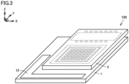
Fig. 3 is a perspective view schematically illustrating the configuration of the infrared sensor according to the first embodiment. -
Fig. 4 is a cross-sectional view schematically illustrating a configuration of the infrared sensor according to a modification to the first embodiment. -
Fig. 5 is a top view schematically illustrating the configuration of the infrared sensor according to the modification to the first embodiment. -
Fig. 6 is a perspective view schematically illustrating the configuration of the infrared sensor according to the modification to the first embodiment. -
Fig. 7 is a perspective view schematically illustrating another method of manufacturing the infrared sensor according to the first embodiment. -
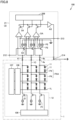
Fig. 8 is a circuit diagram schematically illustrating the configuration of the infrared sensor according to the first embodiment. -
Fig. 9 is a circuit diagram schematically illustrating a configuration of a first semiconductor substrate according to the first embodiment. -
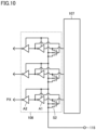
Fig. 10 is a circuit diagram schematically illustrating a configuration of a voltage regulation circuit of the first semiconductor substrate according to the first embodiment. -
Fig. 11 is a cross-sectional view schematically illustrating a configuration of an infrared sensor according to a second embodiment. -
Fig. 12 is a cross-sectional view schematically illustrating a configuration of an infrared sensor according to a third embodiment. -
Fig. 13 is a cross-sectional view schematically illustrating a configuration of an infrared sensor according to a fourth embodiment. -
Fig. 14 is a cross-sectional view schematically illustrating a configuration of an infrared sensor according to a fifth embodiment. -
Fig. 15 is a cross-sectional view schematically illustrating a configuration of an infrared sensor according to a sixth embodiment. -
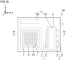
Fig. 16 is a cross-sectional view schematically illustrating the configuration of the infrared sensor according to the sixth embodiment. - Embodiments will be described below based on the drawings. In the following, like or corresponding parts are denoted by like reference signs and an overlapping description is not repeated.
- Referring to
Fig. 1 andFig. 2 , a configuration of aninfrared sensor 100 according to a first embodiment will be described.Fig. 1 is a cross-sectional view along line I-I inFig. 2 . -
Infrared sensor 100 is an infrared sensor for detecting infrared radiation IR incident on aninfrared sensor 100.Infrared sensor 100 according to the present embodiment is a thermal infrared sensor. - As illustrated in
Fig. 1 ,infrared sensor 100 includes afirst semiconductor substrate 1, asecond semiconductor substrate 2, a sealingframe 3, and afirst connection 4.First semiconductor substrate 1 andsecond semiconductor substrate 2 are put on each other at a distance from each other. Each of sealingframe 3 andfirst connection 4 is sandwiched betweenfirst semiconductor substrate 1 andsecond semiconductor substrate 2. - In the present embodiment, the Z axis direction is a direction along the direction in which
first semiconductor substrate 1 andsecond semiconductor substrate 2 are put on each other. The Z axis positive direction is a direction fromfirst semiconductor substrate 1 towardsecond semiconductor substrate 2 along the Z axis direction. The Z axis negative direction is a direction fromsecond semiconductor substrate 2 towardfirst semiconductor substrate 1 along the Z axis direction. The X axis direction is a direction orthogonal to the Z axis direction and along the direction in whichfirst semiconductor substrate 1 extends. The Y axis direction is a direction orthogonal to each of the X axis direction and the Z axis direction. The in-plane direction offirst semiconductor substrate 1 is a direction along the X axis direction and the Y axis direction. - In the present embodiment, infrared radiation IR is incident on
infrared sensor 100 along the Z axis negative direction.Infrared sensor 100 is configured to detect infrared radiation IR incident oninfrared sensor 100 along the Z axis negative direction. In the present embodiment, "infrared radiation IR is incident oninfrared sensor 100 along a certain direction" means that infrared radiation IR having a main component along the certain direction is incident oninfrared sensor 100. Infrared radiation IR therefore may have a component along a direction different from the certain direction. -
First semiconductor substrate 1 includes a firstmain surface 1a, afirst back surface 1b, aninfrared detection element 11, and acontrol circuit 12.First semiconductor substrate 1 may include a plurality ofinfrared detection elements 11. In the present embodiment,first semiconductor substrate 1 includes a plurality ofinfrared detection elements 11. - First
main surface 1a protrudes outside of sealingframe 3 along the in-plane direction (the X axis direction and the Y axis direction) offirst semiconductor substrate 1. Firstmain surface 1a has a flat surface. First backsurface 1b is opposed to firstmain surface 1a. First backsurface 1b therefore extends along the in-plane direction (the X axis direction and the Y axis direction) of firstmain surface 1a on the side opposite tosecond semiconductor substrate 2 with respect to firstmain surface 1a. -
Infrared detection element 11 is arranged on firstmain surface 1a.Infrared detection element 11 is configured to generate a detection signal when infrared radiation IR is incident oninfrared detection element 11. Thus,first semiconductor substrate 1 is formed as an infrared sensor substrate.Infrared detection element 11 is, for example, an element employing MEMS (Micro Electro Mechanical Systems) technology, such as a diode, a resistive bolometer, a ferroelectric thin film, and a thermoelectric element. - In the present embodiment, infrared radiation IR is incident on
infrared detection element 11 throughsecond semiconductor substrate 2 along the Z axis negative direction.Infrared detection element 11 is therefore arranged to facesecond semiconductor substrate 2.Infrared sensor 100 is configured to detect infrared radiation IR incident oninfrared detection element 11 throughsecond semiconductor substrate 2. As described later,infrared sensor 100 may be configured to detect infrared radiation IR incident oninfrared detection element 11 throughfirst back surface 1b offirst semiconductor substrate 1. - In the present embodiment, a pixel PX is formed of two
infrared detection elements 11 as a unit. A plurality of pixels PX form a pixel array PXA.Control circuit 12 is configured to control a plurality ofinfrared detection elements 11.Control circuit 12 is configured to control a plurality of pixels PX. The detailed configuration and operation of pixel PX andcontrol circuit 12 will be described later. -
First semiconductor substrate 1 may further include a not-illustrated support leg. The support leg is arranged on firstmain surface 1a.Infrared detection element 11 may be held in the air above firstmain surface 1a by the support leg. That is,infrared detection element 11 may be arranged at a distance from firstmain surface 1a by the support leg. -
Second semiconductor substrate 2 extends along the in-plane direction (the X axis direction and the Y axis direction) of firstmain surface 1a.Second semiconductor substrate 2 is arranged at a distance fromfirst semiconductor substrate 1.Second semiconductor substrate 2 facesfirst semiconductor substrate 1.Second semiconductor substrate 2 faces in parallel tofirst semiconductor substrate 1. The distance betweenfirst semiconductor substrate 1 andsecond semiconductor substrate 2 along the Z axis direction is the same as the dimension of sealingframe 3 andfirst connection 4 along the Z axis direction. -
Second semiconductor substrate 2 includes a secondmain surface 2a, asecond back surface 2b, and asignal processing circuit 21. Secondmain surface 2a faces firstmain surface 1a. Secondmain surface 2a faces firstmain surface 1a at a distance from firstmain surface 1a. Secondmain surface 2a protrudes outside of sealingframe 3 along the in-plane direction (the X axis direction and the Y axis direction) of firstmain surface 1a. Second backsurface 2b is opposed to secondmain surface 2a. Second backsurface 2b therefore extends along the in-plane direction (the X axis direction and the Y axis direction) of secondmain surface 2a on the side opposite tofirst semiconductor substrate 1 with respect to secondmain surface 2a. -
Signal processing circuit 21 is configured to process a signal ofinfrared detection element 11. Specifically,signal processing circuit 21 is configured to process a detection signal transmitted frominfrared detection element 11. In the present embodiment,signal processing circuit 21 is configured to process a detection signal transmitted from each of a plurality ofinfrared detection elements 11. Thus,second semiconductor substrate 2 is formed as a signal processing circuit substrate. -
Signal processing circuit 21 includes, for example, a read circuit, an amplifier, a sample hold circuit, an analog/digital converter, and a digital signal processing circuit. The read circuit is configured to read an output signal transmitted from each ofinfrared detection elements 11. The amplifier is configured to amplify a signal transmitted from each ofinfrared detection elements 11. The detailed configuration and operation ofsignal processing circuit 21 will be described later. - In the present embodiment,
second semiconductor substrate 2 includes asecond substrate portion 22 and a second infrared transmitting portion IT2.Second substrate portion 22 and second infrared transmitting portion IT2 are configured to transmit infrared radiation IR. Second infrared transmitting portion IT2 is configured to transmit infrared radiation IR more thansecond substrate portion 22. Second infrared transmitting portion IT2 facesinfrared detection element 11. - Second infrared transmitting portion IT2 contains, for example, an impurity such as phosphorous (P) or boron (B). Thus, second infrared transmitting portion IT2 has a resistivity of, for example, 1 Ω·cm or more. The absorption of infrared radiation IR by second infrared transmitting portion IT2 has a correlation with the resistivity of second infrared transmitting portion IT2. Therefore, the larger the resistivity of second infrared transmitting portion IT2 is, the less infrared radiation IR is absorbed in second infrared transmitting portion IT2. Accordingly, when the resistivity of second infrared transmitting portion IT2 is, for example, 1 Ω·cm or more, absorption of the infrared radiation IR wavelength by
second semiconductor substrate 2 is suppressed. - As illustrated in
Fig. 1 andFig. 2 , sealingframe 3 is connected tofirst semiconductor substrate 1 and tosecond semiconductor substrate 2.Sealing frame 3 surrounds an internal space IS with firstmain surface 1a,infrared detection element 11, and secondmain surface 2a. Internal space IS is hermetically sealed by firstmain surface 1a,infrared detection element 11, secondmain surface 2a, and sealingframe 3. As illustrated inFig. 1 , internal space IS is sandwiched between firstmain surface 1a andinfrared detection element 11, and secondmain surface 2a along the Z axis direction. Each ofinfrared detection element 11 and second infrared transmitting portion IT2 faces internal space IS.First connection 4,control circuit 12, andsignal processing circuit 21 are arranged in a region outside internal space IS. As illustrated inFig. 2 , internal space IS is surrounded by sealingframe 3 around the Z axis. - Gas is unable to move between internal space IS and the region outside internal space IS. Accordingly, internal space IS is thermally insulated. In the present embodiment, internal space IS is sealed in a vacuum state. In the present embodiment, internal space IS is not necessarily sealed in a complete vacuum state.
- As illustrated in
Fig. 1 , sealingframe 3 is sandwiched betweenfirst semiconductor substrate 1 andsecond semiconductor substrate 2 along the direction (Z axis direction) in whichfirst semiconductor substrate 1 andsecond semiconductor substrate 2 are put on each other. A first end in the Z axis direction of sealingframe 3 is in contact with firstmain surface 1a. A second end in the Z axis direction of sealingframe 3 is in contact with secondmain surface 2a.Sealing frame 3 supportsfirst semiconductor substrate 1 andsecond semiconductor substrate 2 along the Z axis direction.Sealing frame 3 therefore mechanically connectsfirst semiconductor substrate 1 andsecond semiconductor substrate 2.Sealing frame 3 does not electrically connectfirst semiconductor substrate 1 andsecond semiconductor substrate 2. - The material of sealing
frame 3 has electrical conductivity. The material of sealingframe 3 is, for example, metal. The shape of sealingframe 3 is annular.Sealing frame 3 has, for example, a hollow prism shape. The shape and dimensions of sealingframe 3 may be determined as appropriate as long asinfrared detection element 11 is surrounded.Sealing frame 3 may further surround, for example,control circuit 12. -
First connection 4 electrically connectsfirst semiconductor substrate 1 andsecond semiconductor substrate 2. Specifically,first connection 4 electrically connectsinfrared detection element 11 andsignal processing circuit 21. The material offirst connection 4 has electrical conductivity.First connection 4 is formed as, for example, a bump. -
First connection 4 is sandwiched betweenfirst semiconductor substrate 1 andsecond semiconductor substrate 2 along the direction (Z axis direction) in whichfirst semiconductor substrate 1 andsecond semiconductor substrate 2 are put on each other. A first end in the Z axis direction offirst connection 4 is in contact with firstmain surface 1a. A second end in the Z axis direction offirst connection 4 is in contact with secondmain surface 2a.First connection 4 therefore supportsfirst semiconductor substrate 1 andsecond semiconductor substrate 2 along the Z axis direction.First connection 4 mechanically connectsfirst semiconductor substrate 1 andsecond semiconductor substrate 2. - Each of sealing
frame 3 andfirst connection 4 is sandwiched between firstmain surface 1a and secondmain surface 2a. Each of sealingframe 3 andfirst connection 4 has the same dimension along the direction (Z axis direction) in whichfirst semiconductor substrate 1 andsecond semiconductor substrate 2 are put on each other. - In the present embodiment, the material of
first connection 4 is the same as the material of sealingframe 3. The melting point offirst connection 4 is therefore the same as the melting point of sealingframe 3. -
Infrared sensor 100 further includes asecond connection 5.Second connection 5 is sandwiched between firstmain surface 1a and secondmain surface 2a. A first end in the Z axis direction ofsecond connection 5 is in contact with firstmain surface 1a. A second end in the Z axis direction ofsecond connection 5 is in contact with secondmain surface 2a.Second connection 5 therefore supportsfirst semiconductor substrate 1 andsecond semiconductor substrate 2 along the Z axis direction.Second connection 5 mechanically connectsfirst semiconductor substrate 1 andsecond semiconductor substrate 2.Second connection 5 does not electrically connectfirst semiconductor substrate 1 andsecond semiconductor substrate 2.Second connection 5 is formed as a dummy bump. - In the present embodiment,
second connection 5 has a higher melting point thanfirst connection 4 and sealingframe 3. For example, when the material offirst connection 4 and sealingframe 3 is indium (In) or indium alloy, the material ofsecond connection 5 is nickel (Ni) or copper (Cu). -
Infrared sensor 100 further includes anantireflective film 6. In the present embodiment,antireflective film 6 is arranged on the side opposite tofirst semiconductor substrate 1 with respect to secondmain surface 2a.Antireflective film 6 coverssecond back surface 2b.Antireflective film 6 overlapsinfrared detection element 11 along the Z axis direction. Infrared radiation IR is therefore incident oninfrared detection element 11 throughantireflective film 6. -
Antireflective film 6 is formed to prevent reflection of infrared radiation IR. In the present embodiment,antireflective film 6 does not need to completely prevent reflection of infrared radiation IR.Antireflective film 6 may be formed to suppress reflection of infrared radiation IR incident onantireflective film 6. -
Antireflective film 6 is, for example, an antireflection coat (AR coat) such as diamond like carbon (DLC) or zinc sulfide (ZnS). - As illustrated in
Fig. 2 ,first connection 4 includes a plurality offirst connection portions 41. Each offirst connection portions 41 electrically connectsfirst semiconductor substrate 1 andsecond semiconductor substrate 2. Each offirst connection portions 41 has, for example, a cylindrical shape. Each offirst connection portions 41 may have the same diameter. -
Second connection 5 includes a plurality ofsecond connection portions 51. Each ofsecond connection portions 51 does not electrically connectfirst semiconductor substrate 1 andsecond semiconductor substrate 2. Each ofsecond connection portions 51 has, for example, a cylindrical shape. Each ofsecond connection portions 51 may have the same diameter. - Second infrared transmitting portion IT2 overlaps
infrared detection element 11 along the direction (Z axis direction) in whichfirst semiconductor substrate 1 andsecond semiconductor substrate 2 are put on each other.Control circuit 12 andsignal processing circuit 21 do not overlapinfrared detection element 11 along the direction (Z axis direction) in whichfirst semiconductor substrate 1 andsecond semiconductor substrate 2 are put on each other.Signal processing circuit 21 is sandwiched betweenfirst connection 4 andsecond connection 5 along the Y axis direction. - As illustrated in
Fig. 2 andFig. 3 , the dimensions in the in-plane direction (the X axis direction and the Y axis direction) offirst semiconductor substrate 1 may be larger than the dimensions in the in-plane direction (the X axis direction and the Y axis direction) ofsecond semiconductor substrate 2. In the present embodiment,control circuit 12 is arranged to overlapsecond semiconductor substrate 2 in the Z axis direction.Control circuit 12 may be arranged so as not to overlapsecond semiconductor substrate 2 in the Z axis direction. InFig. 3 , for convenience of explanation,infrared sensor 100 is illustrated in a simplified form as appropriate. - Referring now to
Fig. 4 to Fig. 6 , a configuration ofinfrared sensor 100 according to a modification to the first embodiment will be described.Fig. 4 is a cross-sectional view along line IV-IV inFig. 5 . - As illustrated in
Fig. 4 ,control circuit 12 according to the modification to the first embodiment faces secondmain surface 2a. Specifically,control circuit 12 facessignal processing circuit 21.Control circuit 12 overlaps signalprocessing circuit 21 along the Z axis direction. - As illustrated in
Fig. 5 ,control circuit 12 includes a firstcontrol circuit portion 12a and a secondcontrol circuit portion 12b. Firstcontrol circuit portion 12a and secondcontrol circuit portion 12b are electrically connected by not-illustrated wiring. Firstcontrol circuit portion 12a andsignal processing circuit 21 are sandwiched betweenfirst connection 4 andsecond connection 5 along the Y axis direction. As illustrated inFig. 5 andFig. 4 , firstcontrol circuit portion 12a facessignal processing circuit 21. - As illustrated in
Fig. 5 andFig. 6 , the dimension along each of the X axis direction and the Y axis direction offirst semiconductor substrate 1 may be the same as the dimension along each of the X axis direction and the Y axis direction ofsecond semiconductor substrate 2. InFig. 6 , for convenience of explanation,infrared sensor 100 is illustrated in a simplified form as appropriate. - Referring now to
Fig. 1 andFig. 7 , a method of manufacturinginfrared sensor 100 according to the first embodiment will be described. - The method of manufacturing
infrared sensor 100 includes step S101 of preparing and step S 102 of electrically connecting. - As illustrated in
Fig. 1 ,first semiconductor substrate 1,second semiconductor substrate 2, sealingframe 3, andfirst connection 4 are prepared. In the present embodiment,second connection 5 is further prepared. - Specifically,
first semiconductor substrate 1 andsecond semiconductor substrate 2 are prepared specifically in accordance with the following process. First, a wafer process is used for a silicon (Si) substrate serving asfirst semiconductor substrate 1 to form pixel array PXA (seeFig. 1 ) andcontrol circuit 12. - Subsequently, a metallized pattern is formed in each of a region in which
sealing frame 3 is arranged in the silicon substrate serving asfirst semiconductor substrate 1 and a region in whichsealing frame 3 is arranged in the silicon substrate serving assecond semiconductor substrate 2. The region in whichsealing frame 3 is arranged is located outside the pixel array. - Specifically, for example, titanium (Ti) or chromium (Cr) and copper (Cu) are successively deposited by sputtering on the entire first
main surface 1a offirst semiconductor substrate 1. Subsequently, a resist pattern is formed by photolithography (lithography technology). Then, nickel (Ni) and gold (Au) are successively formed by electroplating on firstmain surface 1a. Subsequently, the resist pattern is removed. The underlying film is removed. The metallized pattern is thus formed onfirst semiconductor substrate 1. - In
second semiconductor substrate 2, the metallized pattern is formed in the same manner as infirst semiconductor substrate 1.Second semiconductor substrate 2 may be produced separately fromfirst semiconductor substrate 1.Second semiconductor substrate 2 thus may be produced by a conventional common silicon wafer process. - Then, silicon etching or the like is performed by micromachining technology on each of the silicon substrate serving as
first semiconductor substrate 1 and the silicon substrate serving assecond semiconductor substrate 2.First semiconductor substrate 1 andsecond semiconductor substrate 2 are thus produced. - Then, each of sealing
frame 3 andfirst connection 4 is sandwiched between firstmain surface 1a,infrared detection element 11, and secondmain surface 2a, whereby internal space IS is surrounded by firstmain surface 1a,infrared detection element 11, secondmain surface 2a, and sealingframe 3, and internal space IS is hermetically sealed.Second connection 5 is sandwiched together with sealingframe 3 andfirst connection 4 between firstmain surface 1a and secondmain surface 2a. - Specifically, the first end of sealing
frame 3 is bonded to firstmain surface 1a. The first end offirst connection 4 is bonded to firstmain surface 1a. The second end of sealingframe 3 is bonded to secondmain surface 2a. The second end offirst connection 4 is bonded to secondmain surface 2a. Thus, internal space IS is sealed.First semiconductor substrate 1 andsecond semiconductor substrate 2 are connected to each other with sealingframe 3,first connection 4, andsecond connection 5 interposed.First semiconductor substrate 1 andsecond semiconductor substrate 2 are arranged at a distance from each other by the dimension along the Z axis direction of sealingframe 3,first connection 4, andsecond connection 5. - In the present embodiment, internal space IS is hermetically sealed by first
main surface 1a,infrared detection element 11, secondmain surface 2a, and sealingframe 3 in a vacuum atmosphere. Specifically, firstmain surface 1a and secondmain surface 2a are bonded to sealingframe 3 in a vacuum atmosphere with the temperature offirst semiconductor substrate 1 andsecond semiconductor substrate 2 kept at a temperature equal to or higher than the melting point of the material of sealingframe 3. - Each of sealing
frame 3 andfirst connection 4 is sandwiched between firstmain surface 1a,infrared detection element 11, and secondmain surface 2a, wherebyinfrared detection element 11 andsignal processing circuit 21 are electrically connected byfirst connection 4. Specifically, the first end offirst connection 4 is electrically connected toinfrared detection element 11 or not-illustrated wiring connected toinfrared detection element 11. The second end offirst connection 4 is electrically connected to signalprocessing circuit 21 or not-illustrated wiring connected to signalprocessing circuit 21. - As illustrated in
Fig. 7 , in manufacturing, afirst wafer 10 serving as first semiconductor substrate 1 (seeFig. 1 ) and asecond wafer 20 serving as second semiconductor substrate 2 (seeFig. 1 ) may be used. The process may be performed in a wafer state to produce first semiconductor substrate 1 (seeFig. 1 ) and second semiconductor substrate 2 (seeFig. 1 ). InFig. 7 , onesealing frame 3, onefirst connection 4, and onesecond connection 5 are illustrated, but a plurality of sealingframes 3,first connections 4, andsecond connections 5 are prepared. - As described above, the sealing of internal space IS and the electrical connection between
infrared detection element 11 andsignal processing circuit 21 are performed simultaneously. - Referring to
Fig. 1 , the operation principle and sensitivity ofinfrared sensor 100 according to the first embodiment will now be described. -
Infrared sensor 100 is configured to convert infrared radiation IR absorbed byinfrared sensor 100 into heat. Specifically,infrared detection element 11 is configured to convert infrared radiation IR absorbed byinfrared detection element 11 into heat.Infrared sensor 100 is configured to convert temperature change caused by the converted heat into an electrical signal.Infrared sensor 100 is therefore configured to detect infrared radiation IR based on the temperature change ofinfrared detection element 11. - Thus, the temperature change of
infrared detection element 11 due to temperature change of internal space IS is suppressed, thereby improving the sensitivity ofinfrared sensor 100. - Specifically, as illustrated in
Fig. 1 , sinceinfrared detection element 11 faces internal space IS, the temperature ofinfrared detection element 11 changes when the temperature of internal space IS changes. The temperature of internal space IS changes, for example, with the convection of gas filled in internal space IS and heat transfer. - When internal space IS is sealed in a vacuum state, the gas convection and heat transfer is suppressed. Thus, the temperature change of
infrared detection element 11 due to the temperature change of internal space IS is suppressed.Infrared sensor 100 according to the present embodiment therefore has high sensitivity. - Referring now to
Fig. 8 to Fig. 10 , a circuit configuration ofinfrared sensor 100 according to the first embodiment will be described. - As illustrated in
Fig. 8 andFig. 9 ,first semiconductor substrate 1 includes a plurality of column signal lines 1C, a plurality ofrow signal lines 1L, and a plurality of pixels PX. Each of column signal lines 1C extends along the Y axis direction (seeFig. 1 ). One end of each of column signal lines 1C is connected to a corresponding one of a plurality ofoutput terminals 4a. Each ofoutput terminals 4a is connected tosecond semiconductor substrate 2 by a corresponding one offirst connection portions 41. - Each of
row signal lines 1L extends along the X axis direction (seeFig. 1 ). - A plurality of pixels PX are arranged in a two-dimensional array along the Y axis direction (see
Fig. 1 ) and the X axis direction (seeFig. 2 ). Pixel array PXA is thus formed. Each of pixels PX includes twoinfrared detection elements 11 connected to each other. One of twoinfrared detection elements 11 is connected to one column signal line 1C among a plurality of column signal lines 1C. The other of twoinfrared detection elements 11 is connected to onerow signal line 1L among a plurality ofrow signal lines 1L. -
Control circuit 12 includes a plurality of first switching elements S1, a plurality of first current sources P1, a first columnselect circuit 106, a rowselect circuit 107, and avoltage regulation circuit 108. Each of first switching elements S1 is connected to a corresponding one of column signal lines 1C. - Each of first current sources P1 is connected to a corresponding one of column signal lines 1C. Each of first current sources P1 is connected to column signal line 1C through first switching element S1. Each of first current sources P1 is connected to a plurality of pixels PX through column signal line 1C.
- First column
select circuit 106 is configured to selectively connect each of first current sources P1 toinfrared detection element 11 through the corresponding column signal line 1C. First columnselect circuit 106 is configured to selectively connect each of first current sources P1 to the correspondinginfrared detection element 11 through firstswitching element S 1. - Row
select circuit 107 is configured to selectively apply a voltage to a plurality ofinfrared detection elements 11 through a plurality ofrow signal lines 1L.Voltage regulation circuit 108 is configured to apply a variable voltage to twoinfrared detection elements 11 of each of pixels PX through a plurality ofrow signal lines 1L. Rowselect circuit 107 andvoltage regulation circuit 108 are configured as a first voltage source. -
Fig. 10 is a circuit diagram illustrating the configuration ofvoltage regulation circuit 108 in detail. InFig. 8 andFig. 9 ,voltage regulation circuit 108 is on the right side of rowselect circuit 107 in the drawing sheet, whereas inFig. 10 ,voltage regulation circuit 108 is on the left side of rowselect circuit 107 in the drawing sheet. - As illustrated in
Fig. 10 ,voltage regulation circuit 108 includes a plurality of second switching elements S2, a plurality of first amplifiers A1, and a plurality of second amplifiers A2. Each of second switching elements S2, each of first amplifiers A1, and each of second amplifiers A2 are connected to a corresponding one ofrow signal lines 1L. A plurality of second switching elements S2, first amplifiers A1, and a plurality of second amplifiers A2 are configured as a buffer circuit. An output voltage of the buffer circuit changes with a voltage value input from the power supply of the pixels. - As described above,
first semiconductor substrate 1 has at least a means for enabling voltage to be applied to pixel array PXA and current to flow through pixel array PXA. That is, as illustrated inFig. 8 ,first semiconductor substrate 1 has first current sources P1, first columnselect circuit 106, rowselect circuit 107, andvoltage regulation circuit 108 as the means for applying voltage and feeding current to pixel array PXA. A plurality of pixels PX arranged in a two-dimensional array can be selected one by one by first columnselect circuit 106 and rowselect circuit 107. A variable voltage can be applied to twoinfrared detection elements 11 of each of pixels PX by rowselect circuit 107 andvoltage regulation circuit 108. - As illustrated in
Fig. 8 ,second semiconductor substrate 2 includes a plurality ofinput terminals 4b, a plurality of third switching elements S3, a plurality of fourth switching elements S4, a plurality of second current sources P2, a plurality of operation amplifiers OA, a second columnselect circuit 206, and a third amplifier A3. - Each of
input terminals 4b ofsignal processing circuit 21 is connected to a corresponding one ofoutput terminals 4a offirst semiconductor substrate 1 byfirst connection portion 41. Each of third switching elements S3, each of fourth switching elements S4, each of second current sources P2, and each of operation amplifiers OA are connected to a corresponding one ofinput terminals 4b. Each ofinput terminals 4b is connected to the inverting input terminal of operation amplifier OA. Each ofinput terminals 4b is connected to the non-inverting input terminal of operation amplifier OA by third switching element S3 and second current source P2. A plurality of second current sources P2 are connected to twoinfrared detection elements 11 of each of pixels PX by a plurality ofinput terminals 4b, a plurality offirst connection portions 41, a plurality ofoutput terminals 4a, and a plurality of column signal lines 1C. - A bias voltage is applied to the non-inverting input terminal of operation amplifier OA through a first
external terminal 213. Third switching elements S3 connect or disconnect a plurality ofinput terminals 4b and a plurality of second power supplies in accordance with a control voltage input through a secondexternal terminal 212. Third switching elements S3 are connected (turned on) wheninfrared sensor 100 operates and captures an image. Thirdexternal terminal 214 is connected to the outside. - A plurality of operation amplifiers OA are configured to operate as integral circuits. Second column
select circuit 206 is configured to selectively send output signals from a plurality of operation amplifiers OA to third amplifier A3 by a plurality of fourth switching elements S4. Third amplifier A3 is configured to amplify a signal. Third amplifier A3 is configured to output the amplified signal finally frominfrared sensor 100. - When
infrared sensor 100 operates and captures an image, a plurality of pixels PX arranged in a two-dimensional array can be selected one by one by second columnselect circuit 206 ofsecond semiconductor substrate 2 and rowselect circuit 107 offirst semiconductor substrate 1. Wheninfrared sensor 100 operates and captures an image, second current source P2 ofsecond semiconductor substrate 2 is connected toinfrared detection element 11. Wheninfrared sensor 100 operates and captures an image, first current source P1 offirst semiconductor substrate 1 is not connected toinfrared detection element 11. A variable voltage is applied toinfrared detection element 11 by rowselect circuit 107 andvoltage regulation circuit 108. - The terminal-to-terminal voltage of second current source P2 connected to
infrared detection element 11 and the terminal-to-terminal voltage of second current source P2 connected to input terminal 4b are input to operation amplifier OA. As a result, third amplifier A3 finally outputs a signal in which a voltage drop distribution due to wiring resistance in the horizontal direction is subtracted. -
Second semiconductor substrate 2 is configured such that the output signals of a plurality ofinfrared detection elements 11 that are input fromfirst semiconductor substrate 1 through a plurality offirst connection portions 41 are differentially amplified and output by the integral circuits of operation amplifiers OA. Since output signals of a plurality ofinfrared detection elements 11 are amplified and the output signals are converted into digital data by a not-illustrated analog/digital converter, a satisfactory output signal can be finally output without being influenced by a circuit at a subsequent stage. -
Second semiconductor substrate 2 may perform signal processing by a not-illustrated digital signal processing circuit after converting the output signals of a plurality ofinfrared detection elements 11 into digital data by the not-illustrated analog/digital converter. The digital data has high noise immunity and therefore is suitable for operation processing. The not-illustrated digital signal processing circuit is mounted onsecond semiconductor substrate 2. - Feedback may be performed with an output signal of the not-illustrated digital signal processing circuit so that even more optimum control can be performed on
second semiconductor substrate 2 ofinfrared sensor 100. An output signal of the not-illustrated digital signal processing circuit may be converted into an analog voltage signal by a not-illustrated digital/analog converter and thereafter sent tofirst semiconductor substrate 1 throughfirst connection portion 41. The not-illustrated digital/analog converter may be mounted onfirst semiconductor substrate 1. The not-illustrated digital/analog converter mounted onfirst semiconductor substrate 1 can transfer a signal kept in the form of a digital signal. - Although the configuration in which each of
output terminals 4a connected to a corresponding one of column signal lines 1C offirst semiconductor substrate 1 is connected to input terminal 4b ofsecond semiconductor substrate 2 byfirst connection portion 41 has been described, the circuit configuration of each offirst semiconductor substrate 1 andsecond semiconductor substrate 2 is not limited thereto and can be selected as appropriate depending on the applications. For example, each ofoutput terminals 4a connected to a corresponding one ofrow signal lines 1L offirst semiconductor substrate 1 may be connected to input terminal 4b ofsecond semiconductor substrate 2 byfirst connection portion 41. - The operation effect of the present embodiment will now be described.
- In
infrared sensor 100 according to the present embodiment, as illustrated inFig. 1 , each of sealingframe 3 andfirst connection 4 is sandwiched between firstmain surface 1a and secondmain surface 2a. Each of sealingframe 3 andfirst connection 4 therefore can be sandwiched by firstmain surface 1a and secondmain surface 2a. Accordingly, sealingframe 3 andfirst connection 4 can be sandwiched together by firstmain surface 1a and secondmain surface 2a. Therefore, the sealing of internal space IS and the electrical connection betweenfirst semiconductor substrate 1 andsecond semiconductor substrate 2 can be performed simultaneously. Accordingly, increase of the manufacturing cost ofinfrared sensor 100 can be suppressed. - As illustrated in
Fig. 1 ,infrared sensor 100 further includesantireflective film 6.Antireflective film 6 is formed to prevent reflection of infrared radiation IR. Therefore, occurrence of a stray light component due to reflected light of the incident infrared radiation IR can be suppressed compared with whenantireflective film 6 is not provided. The stray light component is a component resulting from unnecessary infrared scattering. Accordingly, reduction of sensitivity ofinfrared sensor 100 due to the stray light component can be suppressed. - As illustrated in
Fig. 1 ,second semiconductor substrate 2 includessecond substrate portion 22 and second infrared transmitting portion IT2. Second infrared transmitting portion IT2 is configured to transmit infrared radiation IR more thansecond substrate portion 22. The strength of infrared radiation IR incident oninfrared detection element 11 therefore can be enhanced compared with when infrared radiation IR is incident oninfrared detection element 11 throughsecond substrate portion 22. Accordingly, the sensitivity ofinfrared sensor 100 can be enhanced. - As illustrated in
Fig. 1 ,infrared sensor 100 further includessecond connection 5. The load applied to sealingframe 3 andfirst connection 4 therefore can be distributed compared with when only sealingframe 3 andfirst connection 4 are sandwiched between firstmain surface 1a and secondmain surface 2a. Accordingly,first semiconductor substrate 1 andsecond semiconductor substrate 2 can be arranged such thatfirst semiconductor substrate 1 andsecond semiconductor substrate 2 face in parallel to each other even when a load is applied to sealingframe 3 andfirst connection 4. - As illustrated in
Fig. 1 ,infrared sensor 100 further includessecond connection 5. Firstmain surface 1a and secondmain surface 2a therefore can be connected firmly compared with when only sealingframe 3 andfirst connection 4 are sandwiched between firstmain surface 1a and secondmain surface 2a. -
Second connection 5 has a higher melting point thanfirst connection 4. Therefore, the mechanical strength of bonding betweenfirst semiconductor substrate 1 andsecond semiconductor substrate 2 can be enhanced. - More specifically,
first semiconductor substrate 1 andsecond semiconductor substrate 2 are bonded by sealingframe 3,first connection 4, andsecond connection 5 in accordance with the following steps. First, sealingframe 3,first connection 4, andsecond connection 5 are arranged betweenfirst semiconductor substrate 1 andsecond semiconductor substrate 2.Sealing frame 3 andfirst connection 4 are melted by heating at a temperature higher than the melting point of sealingframe 3 andfirst connection 4 and lower than the melting point ofsecond connection 5. In a state in whichfirst semiconductor substrate 1 andsecond semiconductor substrate 2 are at a distance from each other by the dimension ofsecond connection 5,first semiconductor substrate 1 andsecond semiconductor substrate 2 are mechanically and electrically connected by sealingframe 3 andfirst connection 4. On the other hand, whenfirst connection 4 is melted,second connection 5 is not melted. Therefore, reduction of the strength ofsecond connection 5 due to the melting ofsecond connection 5 can be suppressed. Reduction of the parallelism (the evenness of the distance) betweenfirst semiconductor substrate 1 andsecond semiconductor substrate 2 due to the melting ofsecond connection 5 can be suppressed. The mechanical strength offirst semiconductor substrate 1 andsecond semiconductor substrate 2 therefore can be enhanced. Displacement ofsecond connection 5 due to the melting ofsecond connection 5 can be suppressed.First semiconductor substrate 1 andsecond semiconductor substrate 2 therefore can be bonded to each other at high accuracy. - The material of sealing
frame 3 has electrical conductivity.Sealing frame 3 therefore can be melted at a temperature at which the material offirst connection 4 having electrical conductivity can be melted. Accordingly, sealingframe 3 andfirst connection 4 can be melted at the same temperature. The manufacturing steps therefore can be simplified compared with when sealingframe 3 andfirst connection 4 are melted at different temperatures. - The material of
first connection 4 is the same as the material of sealingframe 3. The melting point offirst connection 4 is therefore the same as the melting point of sealingframe 3. Thus, sealingframe 3 andfirst connection 4 can be melted at the same temperature. Accordingly, the manufacturing steps can be simplified compared with when sealingframe 3 andfirst connection 4 are melted at different temperatures. - As illustrated in
Fig. 1 , internal space IS is sealed in a vacuum state. Therefore, occurrence of heat transfer and convection of gas in internal space IS can be suppressed compared with when the pressure of internal space IS is the atmospheric pressure. Accordingly, reduction of thermal resistance of internal space IS can be suppressed. Thus, escape of heat frominfrared detection element 11 to internal space IS by heat transfer can be suppressed. The sensitivity ofinfrared sensor 100 therefore can be enhanced. - As illustrated in
Fig. 1 ,second connection 5 does not electrically connectfirst semiconductor substrate 1 andsecond semiconductor substrate 2.Second connection 5 therefore is not in contact with the electrode material of each offirst semiconductor substrate 1 andsecond semiconductor substrate 2. Accordingly, diffusion ofsecond connection 5 to the electrode materials offirst semiconductor substrate 1 andsecond semiconductor substrate 2 can be suppressed. - In
infrared sensor 100 according to the modification to the present embodiment, as illustrated inFig. 4 ,control circuit 12 facessignal processing circuit 21. Therefore, the dimensions along the in-plane direction (the X axis direction and the Y axis direction) offirst semiconductor substrate 1 can be reduced compared with whencontrol circuit 12 does not facesignal processing circuit 21. Accordingly, the dimensions along the X axis direction and the Y axis direction ofinfrared sensor 100 can be reduced. - In the method of manufacturing
infrared sensor 100 according to the present embodiment, as illustrated inFig. 1 , each of sealingframe 3 andfirst connection 4 is sandwiched between firstmain surface 1a,infrared detection element 11, and secondmain surface 2a, whereby internal space IS is surrounded by firstmain surface 1a,infrared detection element 11, secondmain surface 2a, and sealingframe 3, and internal space IS is hermetically sealed. Each of sealingframe 3 andfirst connection 4 is sandwiched between firstmain surface 1a,infrared detection element 11, and secondmain surface 2a, wherebyinfrared detection element 11 andsignal processing circuit 21 are electrically connected byfirst connection 4. Therefore, the sealing of internal space IS and the electrical connection betweenfirst semiconductor substrate 1 andsecond semiconductor substrate 2 can be performed at the same time. Thus, the manufacturing steps ofinfrared sensor 100 can be simplified. Accordingly, increase of the manufacturing cost ofinfrared sensor 100 can be suppressed. - As illustrated in
Fig. 1 , internal space IS is hermetically sealed by firstmain surface 1a,infrared detection element 11, secondmain surface 2a, and sealingframe 3 in a vacuum atmosphere. Internal space IS therefore can be sealed in a vacuum state. Accordingly, the sensitivity ofinfrared sensor 100 can be enhanced. - As illustrated in
Fig. 1 ,second connection 5 is further prepared.Second connection 5 is sandwiched together with sealingframe 3 andfirst connection 4 between firstmain surface 1a and secondmain surface 2a. The load applied to sealingframe 3 andfirst connection 4 therefore can be distributed compared with when only sealingframe 3 andfirst connection 4 are sandwiched between firstmain surface 1a and secondmain surface 2a. Accordingly,first semiconductor substrate 1 andsecond semiconductor substrate 2 can be arranged such thatfirst semiconductor substrate 1 andsecond semiconductor substrate 2 face in parallel to each other. - Referring now to
Fig. 11 , a configuration ofinfrared sensor 100 according to a second embodiment will be described. The second embodiment has the same configuration, manufacturing method, and operation effects as the modification to the first embodiment described above, unless otherwise specified. The same configuration as the modification to the first embodiment described above is denoted by the same reference sign and will not be further elaborated. - As illustrated in
Fig. 11 , secondmain surface 2a according to the present embodiment includes a second main surface portion P and a depressed portion G. Second main surface portion P and depressed portion G face internal space IS. Second main surface portion P is a flat surface. Depressed portion G is provided at a position facinginfrared detection element 11 to be depressed from second main surface portion P. Specifically, depressed portion G is provided at a position facinginfrared detection element 11 to be depressed from second main surface portion P along the direction (Z axis direction) in whichfirst semiconductor substrate 1 andsecond semiconductor substrate 2 are put on each other. Depressed portion G overlapsinfrared detection element 11 along the Z axis direction. In the present embodiment, depressed portion G is provided in second infrared transmitting portion IT2. - The operation effect of the present embodiment will now be described.
- In
infrared sensor 100 according to the present embodiment, as illustrated inFig. 11 , depressed portion G is provided at a position facinginfrared detection element 11 to be depressed from second main surface portion P. The volume of internal space IS is therefore large compared with when secondmain surface 2a is entirely flat. Temperature change of internal space IS can be suppressed with a larger volume of internal space IS. Therefore, the sensitivity ofinfrared sensor 100 can be enhanced. - Fluctuations of the degree of vacuum due to temperature change of gas escaping from
first semiconductor substrate 1,second semiconductor substrate 2, and the like are smaller with a larger volume of internal space IS. Accordingly, even when the escaping gas intrudes into internal space IS, fluctuations of the degree of vacuum due to the escaping gas can be suppressed. The escaping gas is gas released from the members. - As illustrated in
Fig. 11 , depressed portion G is provided at a position facinginfrared detection element 11 to be depressed from second main surface portion P. Therefore, the thickness ofsecond semiconductor substrate 2 at depressed portion G is smaller than the thickness ofsecond semiconductor substrate 2 in a region in which depressed portion G is not provided. That is,second semiconductor substrate 2 is thinned at depressed portion G. Accordingly,second semiconductor substrate 2 has a high transmittivity at depressed portion G. Thus, the strength of infrared radiation IR incident oninfrared detection element 11 can be enhanced. Therefore, the sensitivity ofinfrared sensor 100 can be enhanced. - Referring now to
Fig. 12 , a configuration ofinfrared sensor 100 according to a third embodiment will be described. The third embodiment has the same configuration, manufacturing method, and operation effects as the modification to the first embodiment described above, unless otherwise specified. The same configuration as the modification to the first embodiment described above is denoted by the same reference sign and will not be further elaborated. - In the present embodiment, infrared radiation IR is incident on
infrared detection element 11 throughfirst back surface 1b along the Z axis positive direction.Infrared detection element 11 is configured to detect infrared radiation IR incident oninfrared detection element 11 throughfirst back surface 1b along the Z axis direction. - As illustrated in
Fig. 12 ,first semiconductor substrate 1 according to the present embodiment includes afirst substrate portion 13 and a first infrared transmitting portion IT1.First substrate portion 13 and the infrared transmitting portion are configured to transmit infrared radiation IR. First infrared transmitting portion IT1 is configured to transmit infrared radiation IR more thanfirst substrate portion 13. First infrared transmittingportion IT 1 facesinfrared detection element 11. First infrared transmitting portion IT1 is arranged to overlapinfrared detection element 11 in the Z axis direction. - First infrared transmitting portion IT1 contains, for example, an impurity such as phosphorous (P) or boron (B). Thus, first infrared transmitting portion IT1 has a resistivity of, for example, 1 Ω·cm or more.
- The absorption of infrared radiation IR by first infrared transmitting portion IT1 has a correlation with the resistivity of first infrared transmitting portion IT1. Therefore, the larger the resistivity of first infrared transmitting portion IT1 is, the less infrared radiation IR is absorbed in first infrared transmitting portion IT1. Accordingly, when the resistivity of first infrared transmitting portion IT1 is, for example, 1 Ω·cm or more, absorption of the infrared radiation IR wavelength by
first semiconductor substrate 1 is suppressed. The configuration of first infrared transmitting portion IT1 may be the same as the configuration of second infrared transmitting portion IT2 except for the position where first infrared transmitting portion IT1 is arranged. - The operation effect of the present embodiment will now be described.
- In
infrared sensor 100 according to the present embodiment, as illustrated inFig. 12 ,first semiconductor substrate 1 includesfirst substrate portion 13 and first infrared transmitting portion IT1. First infrared transmitting portion IT1 is configured to transmit infrared radiation IR more thanfirst substrate portion 13. The strength of infrared radiation IR incident oninfrared detection element 11 therefore can be enhanced compared with when infrared radiation IR is incident oninfrared detection element 11 throughfirst substrate portion 13. Accordingly, the sensitivity ofinfrared sensor 100 can be enhanced. - As illustrated in
Fig. 12 , first infrared transmitting portion IT1 is arranged to overlapinfrared detection element 11 in the Z axis direction. Infrared radiation IR is therefore incident oninfrared detection element 11 through first infrared transmitting portion IT1 even when infrared radiation IR is incident onfirst semiconductor substrate 1 from thefirst back surface 1b side offirst semiconductor substrate 1. Therefore,infrared detection element 11 can be detected even when infrared radiation IR is incident onfirst semiconductor substrate 1 from thefirst back surface 1b side. - Referring now to
Fig. 13 , a configuration ofinfrared sensor 100 according to a fourth embodiment will be described. The fourth embodiment has the same configuration, manufacturing method, and operation effects as the third embodiment described above, unless otherwise specified. The same configuration as the third embodiment described above is denoted by the same reference sign and will not be further elaborated. - As illustrated in
Fig. 13 , secondmain surface 2a according to the present embodiment includes a second main surface portion P and a depressed portion G. Second main surface portion P and depressed portion G face internal space IS. Second main surface portion P is a flat surface. Depressed portion G is provided at a position facinginfrared detection element 11 to be depressed from second main surface portion P. Specifically, depressed portion G is provided at a position facinginfrared detection element 11 to be depressed from second main surface portion P along the direction (Z axis direction) in whichfirst semiconductor substrate 1 andsecond semiconductor substrate 2 are put on each other. Depressed portion G overlapsinfrared detection element 11 along the Z axis direction. Depressed portion G may at least partially overlapinfrared detection element 11 along the Z axis direction. - The operation effect of the present embodiment will now be described.
- In
infrared sensor 100 according to the present embodiment, as illustrated inFig. 13 , depressed portion G is provided at a position facinginfrared detection element 11 to be depressed from second main surface portion P. Therefore, the sensitivity ofinfrared sensor 100 can be enhanced. - Thus, the sensitivity of
infrared sensor 100 can be enhanced even when infrared radiation IR is incident oninfrared detection element 11 throughfirst back surface 1b. - Referring now to
Fig. 14 , a configuration ofinfrared sensor 100 according to a fifth embodiment will be described. The fifth embodiment has the same configuration, manufacturing method, and operation effects as the third embodiment described above, unless otherwise specified. The same configuration as the third embodiment described above is denoted by the same reference sign and will not be further elaborated. - As illustrated in
Fig. 14 ,infrared sensor 100 according to the present embodiment further includesantireflective film 6.Antireflective film 6 is arranged on the side opposite tosecond semiconductor substrate 2 with respect to firstmain surface 1a.Antireflective film 6 coversfirst back surface 1b.Antireflective film 6 is formed to prevent reflection of infrared radiation IR.Antireflective film 6 may have the same configuration as the configuration ofantireflective film 6 described in the first embodiment except for the position whereantireflective film 6 is arranged. - The operation effect of the present embodiment will now be described.
- In
infrared sensor 100 according to the present embodiment,infrared sensor 100 further includesantireflective film 6.Antireflective film 6 is arranged on the side opposite to secondmain surface 2a with respect to firstmain surface 1a.Antireflective film 6 therefore covers first backsurface 1b. Accordingly, occurrence of a stray light component due to reflection of infrared radiation IR can be suppressed even when infrared radiation IR is incident oninfrared detection element 11 from thefirst back surface 1b side offirst semiconductor substrate 1. Thus, the incidence of infrared radiation IR scattered infirst semiconductor substrate 1 oninfrared detection element 11 can be suppressed. The sensitivity ofinfrared sensor 100 can be enhanced even when infrared radiation IR is incident oninfrared detection element 11 from thefirst back surface 1b side offirst semiconductor substrate 1. - Referring to
Fig. 15 andFig. 16 , a configuration ofinfrared sensor 100 according to a sixth embodiment will be described.Fig. 15 is a cross-sectional view along line XV-XV inFig. 16 . The sixth embodiment has the same configuration, manufacturing method, and operation effects as the modification to the first embodiment described above, unless otherwise specified. The same configuration as the modification to the first embodiment described above is denoted by the same reference sign and will not be further elaborated. - As illustrated in
Fig. 15 ,second connection 5 according to the present embodiment has an outer diameter different from that offirst connection 4. In the present embodiment,second connection 5 has a larger outer diameter thanfirst connection 4. As illustrated inFig. 16 , each ofsecond connection portions 51 ofsecond connection 5 has an outer diameter different from that of each offirst connection portions 4 offirst connection 4.Second connection portion 51 has a larger diameter thanfirst connection portion 41. - For example, when the number of
first connection portions 41 is as small as 10 to 100, the outer diameter ofsecond connection 5 may be larger than the outer diameter offirst connection 4. Thus, the distribution of load applied tofirst connection 4 andsecond connection 5 is adjusted whenfirst connection 4 is bonded tofirst semiconductor substrate 1 andsecond semiconductor substrate 2. In the present embodiment, the outer diameter ofsecond connection 5 is larger than the outer diameter offirst connection 4. However, the outer diameter ofsecond connection 5 may be smaller than the outer diameter offirst connection 4. - The number of
second connection portions 51 ofsecond connection 5 may be different from the number offirst connection portions 41 offirst connection 4. In the present embodiment, the number ofsecond connection portions 51 is smaller than the number offirst connection portions 41. - For example, when the number of
first connection portions 41 is as small as 10 to 100, the number ofsecond connection portions 51 may be larger than the number offirst connection portions 41. Thus, the load applied tofirst connection 4 is distributed tosecond connection 5. In the present embodiment, the number ofsecond connection portions 51 is smaller than the number offirst connection portions 41. However, the number ofsecond connection portions 51 may be larger than the number offirst connection portions 41. - The operation effect of the present embodiment will now be described.
- In
infrared sensor 100 according to the present embodiment, as illustrated inFig. 15 ,second connection 5 has an outer diameter different from that offirst connection 4. The outer diameter ofsecond connection 5 therefore can be adjusted in accordance with the volume of internal space IS, the outer diameter offirst connection 4, and the number of first connection portions 41 (seeFig. 16 ). Thus, the distribution of load applied to sealingframe 3,first connection 4, andsecond connection 5 can be adjusted whenfirst semiconductor substrate 1 andsecond semiconductor substrate 2 are bonded.First semiconductor substrate 1 andsecond semiconductor substrate 2 therefore can be bonded at high accuracy. - As illustrated in
Fig. 16 , the number ofsecond connection portions 51 is different from the number offirst connection portions 41. The number ofsecond connection portions 51 therefore can be adjusted in accordance with the volume of internal space IS, the outer diameter offirst connection 4, the number offirst connection portions 41, and the like. The distribution of load applied to sealingframe 3,first connection 4, andsecond connection 5 can be adjusted when first semiconductor substrate 1 (seeFig. 15 ) andsecond semiconductor substrate 2 are bonded. Therefore, first semiconductor substrate 1 (seeFig. 15 ) andsecond semiconductor substrate 2 can be bonded at high accuracy. - Embodiments disclosed here should be understood as being illustrative rather than being limitative in all respects. The scope of the present disclosure is shown not in the foregoing description but in the claims, and it is intended that all modifications that come within the meaning and range of equivalence to the claims are embraced here.
- 1 first semiconductor substrate, 1a first main surface, 2 second semiconductor substrate, 2a second main surface, 3 sealing frame, 4 first connection, 5 second connection, 6 antireflective film, 11 infrared detection element, 13 first substrate portion, 21 signal processing circuit, 22 second substrate portion, 100 infrared sensor, G depressed portion, IR infrared radiation, IS internal space, IT1 first infrared transmitting portion, IT2 second infrared transmitting portion, P second main surface portion.
Claims (15)
- An infrared sensor comprising:a first semiconductor substrate including a first main surface and an infrared detection element disposed at the first main surface;a second semiconductor substrate including a second main surface facing the first main surface, and a signal processing circuit to process a signal of the infrared detection element;a sealing frame connected to the first semiconductor substrate and the second semiconductor substrate and surrounding an internal space with the first main surface, the infrared detection element, and the second main surface; anda first connection electrically connecting the infrared detection element and the signal processing circuit, whereinthe internal space is hermetically sealed by the first main surface, the infrared detection element, the second main surface, and the sealing frame, andeach of the sealing frame and the first connection is sandwiched between the first main surface and the second main surface.
- The infrared sensor according to claim 1, further comprising an antireflective film disposed on a side opposite to the second semiconductor substrate with respect to the first main surface,
wherein the antireflective film prevents reflection of infrared radiation. - The infrared sensor according to claim 1 or 2, whereinthe first semiconductor substrate includes a first substrate portion and a first infrared transmitting portion to transmit infrared radiation more than the first substrate portion, andthe first infrared transmitting portion faces the infrared detection element.
- The infrared sensor according to claim 1, further comprising an antireflective film disposed on a side opposite to the first semiconductor substrate with respect to the second main surface,
wherein the antireflective film prevents reflection of infrared radiation. - The infrared sensor according to claim 1 or 4, whereinthe second semiconductor substrate includes a second substrate portion and a second infrared transmitting portion to transmit infrared radiation more than the second substrate portion, andthe second infrared transmitting portion faces the infrared detection element.
- The infrared sensor according to any one of claims 1 to 5, whereinthe second main surface includes a second main surface portion and a depressed portion, andthe depressed portion is provided at a position facing the infrared detection element to be depressed from the second main surface portion.
- The infrared sensor according to any one of claims 1 to 6, further comprising a second connection,
wherein the second connection is sandwiched between the first main surface and the second main surface. - The infrared sensor according to claim 7, wherein the second connection has an outer diameter different from an outer diameter of the first connection.
- The infrared sensor according to claim 7 or 8, wherein the second connection has a higher melting point than the first connection and the sealing frame.
- The infrared sensor according to any one of claims 1 to 9, wherein a material of each of the first connection and the sealing frame has electrical conductivity.
- The infrared sensor according to any one of claims 1 to 10, wherein a material of the first connection is same as a material of the sealing frame.
- The infrared sensor according to any one of claims 1 to 11, wherein the internal space is sealed in a vacuum state.
- A method of manufacturing an infrared sensor, comprising the steps of:preparing a first semiconductor substrate including a first main surface and an infrared detection element disposed at the first main surface, a second semiconductor substrate including a second main surface and a signal processing circuit to process a signal of the infrared detection element, a sealing frame, and a first connection; andsandwiching each of the sealing frame and the first connection between the first main surface, the infrared detection element, and the second main surface to surround an internal space by the first main surface, the infrared detection element, the second main surface, and the sealing frame, and hermetically sealing the internal space and electrically connecting the infrared detection element and the signal processing circuit by the first connection.
- The method of manufacturing an infrared sensor according to claim 13, wherein the internal space is hermetically sealed by the first main surface, the infrared detection element, the second main surface, and the sealing frame in a vacuum atmosphere.
- The method of manufacturing an infrared sensor according to claim 13 or 14, whereina second connection is further prepared, andthe second connection is sandwiched together with the sealing frame and the first connection between the first main surface and the second main surface.
Applications Claiming Priority (1)
| Application Number | Priority Date | Filing Date | Title |
|---|---|---|---|
| PCT/JP2020/026226 WO2022003959A1 (en) | 2020-07-03 | 2020-07-03 | Infrared sensor and infrared sensor manufacturing method |
Publications (3)
| Publication Number | Publication Date |
|---|---|
| EP4177962A1 true EP4177962A1 (en) | 2023-05-10 |
| EP4177962A4 EP4177962A4 (en) | 2023-08-16 |
| EP4177962B1 EP4177962B1 (en) | 2025-10-08 |
Family
ID=77549924
Family Applications (1)
| Application Number | Title | Priority Date | Filing Date |
|---|---|---|---|
| EP20943789.6A Active EP4177962B1 (en) | 2020-07-03 | 2020-07-03 | Infrared sensor and infrared sensor manufacturing method |
Country Status (4)
| Country | Link |
|---|---|
| EP (1) | EP4177962B1 (en) |
| JP (1) | JP6932277B1 (en) |
| CN (1) | CN115917761B (en) |
| WO (1) | WO2022003959A1 (en) |
Families Citing this family (1)
| Publication number | Priority date | Publication date | Assignee | Title |
|---|---|---|---|---|
| DE102024105796A1 (en) | 2024-02-29 | 2025-09-04 | Alfred Kärcher SE & Co. KG | Floor cleaning machine and method for operating a floor cleaning machine |
Family Cites Families (14)
| Publication number | Priority date | Publication date | Assignee | Title |
|---|---|---|---|---|
| JPS6252421A (en) * | 1985-09-02 | 1987-03-07 | Fujitsu Ltd | Pyroelectric type temperature detector and its preparation |
| CN101138094B (en) | 2005-03-09 | 2010-10-13 | 旭化成电子材料元件株式会社 | Optical device and method for manufacturing optical device |
| WO2007058280A1 (en) * | 2005-11-16 | 2007-05-24 | Kyocera Corporation | Electronic part sealing board, electronic part sealing board in multiple part form, electronic device using electronic part sealing board, and electronic device fabricating method |
| JP4158830B2 (en) * | 2005-11-25 | 2008-10-01 | 松下電工株式会社 | Method for manufacturing thermal infrared detector |
| WO2011030428A1 (en) * | 2009-09-10 | 2011-03-17 | 株式会社 東芝 | Infrared imaging element |
| JP2012059881A (en) * | 2010-09-08 | 2012-03-22 | Toshiba Corp | Imaging device, imaging module and method for manufacturing imaging device |
| KR101153722B1 (en) * | 2011-03-15 | 2012-06-14 | 한국과학기술원 | System in Package Method of Semi-Active Focal PlanSystem in Package Method of Semi-Active Focal Plane Array sensor using Diode witching e Array sensor using Diode witching |
| JP5791461B2 (en) * | 2011-10-21 | 2015-10-07 | 浜松ホトニクス株式会社 | Photodetector |
| CN102610619B (en) * | 2012-03-29 | 2014-04-16 | 江苏物联网研究发展中心 | Wafer-level vacuum encapsulated infrared focal plane array (IRFPA) device and method for producing same |
| EP2802009B1 (en) * | 2013-05-08 | 2021-03-24 | ams AG | Integrated imaging device for infrared radiation and method of production |
| CN105449008B (en) * | 2014-07-10 | 2017-05-17 | 上海巨哥电子科技有限公司 | Infrared sensor and packaging structure thereof and preparation method thereof |
| JP6828250B2 (en) * | 2016-03-03 | 2021-02-10 | 富士通株式会社 | Photodetector and manufacturing method of photodetector |
| WO2018131216A1 (en) * | 2017-01-12 | 2018-07-19 | 三菱電機株式会社 | Infrared sensor substrate and infrared sensor device |
| JP7237506B2 (en) * | 2018-10-02 | 2023-03-13 | ソニーセミコンダクタソリューションズ株式会社 | Imaging device |
-
2020
- 2020-07-03 CN CN202080102395.XA patent/CN115917761B/en active Active
- 2020-07-03 WO PCT/JP2020/026226 patent/WO2022003959A1/en not_active Ceased
- 2020-07-03 EP EP20943789.6A patent/EP4177962B1/en active Active
- 2020-07-03 JP JP2020572565A patent/JP6932277B1/en active Active
Also Published As
| Publication number | Publication date |
|---|---|
| JP6932277B1 (en) | 2021-09-08 |
| CN115917761B (en) | 2025-04-25 |
| JPWO2022003959A1 (en) | 2022-01-06 |
| WO2022003959A1 (en) | 2022-01-06 |
| EP4177962A4 (en) | 2023-08-16 |
| US20230187459A1 (en) | 2023-06-15 |
| CN115917761A (en) | 2023-04-04 |
| EP4177962B1 (en) | 2025-10-08 |
Similar Documents
| Publication | Publication Date | Title |
|---|---|---|
| US5808350A (en) | Integrated IR, visible and NIR sensor and methods of fabricating same | |
| US7385199B2 (en) | Microbolometer IR focal plane array (FPA) with in-situ mirco vacuum sensor and method of fabrication | |
| JP2016194525A (en) | Device for detecting electromagnetic radiation | |
| CN102874735B (en) | Two-material micro-cantilever, electromagnetic radiation detector and detection method | |
| US20110241154A1 (en) | Optical sensor | |
| US6828545B1 (en) | Hybrid microelectronic array structure having electrically isolated supported islands, and its fabrication | |
| US6627865B1 (en) | Nonplanar integrated optical device array structure and a method for its fabrication | |
| JPH11326037A (en) | Vacuum package for infrared detector and method of manufacturing the same | |
| CN104310300A (en) | Infrared detector integrated with pixel-level condensing lenses and preparation method thereof | |
| CN110140215B (en) | Infrared sensor device | |
| EP4177962B1 (en) | Infrared sensor and infrared sensor manufacturing method | |
| US8168936B2 (en) | Interface techniques for coupling a sensor to a readout circuit | |
| US7943904B2 (en) | Bispectral detection device and bispectral detector comprising said device | |
| US20070194238A1 (en) | Method for production of a device for thermal detection of radiation comprising an active microbolometer and a passive microbolometer | |
| US12622076B2 (en) | Infrared sensor and method of manufacturing infrared sensor | |
| CN104112753A (en) | Infrared detector and infrared imaging system, and preparation methods thereof | |
| JP7466699B2 (en) | Small size close-contact focal image sensor | |
| JP3733847B2 (en) | Thermometer | |
| JP4300305B2 (en) | Thermal infrared image sensor | |
| US7180077B1 (en) | Far infrared photoconductor array | |
| Lange et al. | 6000-element infrared focal plane array for reconnaissance applications | |
| FR3041151A1 (en) | MICROELECTRONIC DEVICE AND METHOD FOR MANUFACTURING THE SAME | |
| CN206516606U (en) | Electrode lead unit and vacuum photoelectric device | |
| US20240194707A1 (en) | Enhanced area getter architecture for wafer-level vacuum packaged uncooled focal plane array | |
| JP2001044400A (en) | Semiconductor infrared detector |
Legal Events
| Date | Code | Title | Description |
|---|---|---|---|
| STAA | Information on the status of an ep patent application or granted ep patent |
Free format text: STATUS: THE INTERNATIONAL PUBLICATION HAS BEEN MADE |
|
| PUAI | Public reference made under article 153(3) epc to a published international application that has entered the european phase |
Free format text: ORIGINAL CODE: 0009012 |
|
| STAA | Information on the status of an ep patent application or granted ep patent |
Free format text: STATUS: REQUEST FOR EXAMINATION WAS MADE |
|
| 17P | Request for examination filed |
Effective date: 20221117 |
|
| AK | Designated contracting states |
Kind code of ref document: A1 Designated state(s): AL AT BE BG CH CY CZ DE DK EE ES FI FR GB GR HR HU IE IS IT LI LT LU LV MC MK MT NL NO PL PT RO RS SE SI SK SM TR |
|
| REG | Reference to a national code |
Ref legal event code: R079 Ipc: G01J0005040000 Ref country code: DE Ref legal event code: R079 Ref document number: 602020060336 Country of ref document: DE Free format text: PREVIOUS MAIN CLASS: H01L0031020000 Ipc: G01J0005040000 |
|
| A4 | Supplementary search report drawn up and despatched |
Effective date: 20230713 |
|
| RIC1 | Information provided on ipc code assigned before grant |
Ipc: H01L 27/146 20060101ALI20230707BHEP Ipc: H01L 27/144 20060101ALI20230707BHEP Ipc: H01L 31/0203 20140101ALI20230707BHEP Ipc: G01J 5/10 20060101ALI20230707BHEP Ipc: G01J 5/04 20060101AFI20230707BHEP |
|
| DAV | Request for validation of the european patent (deleted) | ||
| DAX | Request for extension of the european patent (deleted) | ||
| GRAP | Despatch of communication of intention to grant a patent |
Free format text: ORIGINAL CODE: EPIDOSNIGR1 |
|
| STAA | Information on the status of an ep patent application or granted ep patent |
Free format text: STATUS: GRANT OF PATENT IS INTENDED |
|
| INTG | Intention to grant announced |
Effective date: 20250527 |
|
| RIC1 | Information provided on ipc code assigned before grant |
Ipc: H10F 39/00 20250101ALI20250519BHEP Ipc: G01J 5/00 20220101ALI20250519BHEP Ipc: H10F 77/50 20250101ALI20250519BHEP Ipc: G01J 5/02 20220101ALI20250519BHEP Ipc: H04N 23/23 20230101ALI20250519BHEP Ipc: G01J 5/10 20060101ALI20250519BHEP Ipc: G01J 5/04 20060101AFI20250519BHEP |
|
| GRAS | Grant fee paid |
Free format text: ORIGINAL CODE: EPIDOSNIGR3 |
|
| GRAA | (expected) grant |
Free format text: ORIGINAL CODE: 0009210 |
|
| STAA | Information on the status of an ep patent application or granted ep patent |
Free format text: STATUS: THE PATENT HAS BEEN GRANTED |
|
| AK | Designated contracting states |
Kind code of ref document: B1 Designated state(s): AL AT BE BG CH CY CZ DE DK EE ES FI FR GB GR HR HU IE IS IT LI LT LU LV MC MK MT NL NO PL PT RO RS SE SI SK SM TR |
|
| REG | Reference to a national code |
Ref country code: GB Ref legal event code: FG4D Ref country code: CH Ref legal event code: F10 Free format text: ST27 STATUS EVENT CODE: U-0-0-F10-F00 (AS PROVIDED BY THE NATIONAL OFFICE) Effective date: 20251008 |
|
| REG | Reference to a national code |
Ref country code: DE Ref legal event code: R096 Ref document number: 602020060336 Country of ref document: DE |
|
| REG | Reference to a national code |
Ref country code: IE Ref legal event code: FG4D |
|
| REG | Reference to a national code |
Ref country code: NL Ref legal event code: MP Effective date: 20251008 |
|
| REG | Reference to a national code |
Ref country code: AT Ref legal event code: MK05 Ref document number: 1845170 Country of ref document: AT Kind code of ref document: T Effective date: 20251008 |
|
| PG25 | Lapsed in a contracting state [announced via postgrant information from national office to epo] |
Ref country code: NL Free format text: LAPSE BECAUSE OF FAILURE TO SUBMIT A TRANSLATION OF THE DESCRIPTION OR TO PAY THE FEE WITHIN THE PRESCRIBED TIME-LIMIT Effective date: 20251008 |
|
| PG25 | Lapsed in a contracting state [announced via postgrant information from national office to epo] |
Ref country code: ES Free format text: LAPSE BECAUSE OF FAILURE TO SUBMIT A TRANSLATION OF THE DESCRIPTION OR TO PAY THE FEE WITHIN THE PRESCRIBED TIME-LIMIT Effective date: 20251008 |
|
| REG | Reference to a national code |
Ref country code: LT Ref legal event code: MG9D |
|
| PG25 | Lapsed in a contracting state [announced via postgrant information from national office to epo] |
Ref country code: NO Free format text: LAPSE BECAUSE OF FAILURE TO SUBMIT A TRANSLATION OF THE DESCRIPTION OR TO PAY THE FEE WITHIN THE PRESCRIBED TIME-LIMIT Effective date: 20260108 |
|
| PG25 | Lapsed in a contracting state [announced via postgrant information from national office to epo] |
Ref country code: HR Free format text: LAPSE BECAUSE OF FAILURE TO SUBMIT A TRANSLATION OF THE DESCRIPTION OR TO PAY THE FEE WITHIN THE PRESCRIBED TIME-LIMIT Effective date: 20251008 Ref country code: FI Free format text: LAPSE BECAUSE OF FAILURE TO SUBMIT A TRANSLATION OF THE DESCRIPTION OR TO PAY THE FEE WITHIN THE PRESCRIBED TIME-LIMIT Effective date: 20251008 Ref country code: AT Free format text: LAPSE BECAUSE OF FAILURE TO SUBMIT A TRANSLATION OF THE DESCRIPTION OR TO PAY THE FEE WITHIN THE PRESCRIBED TIME-LIMIT Effective date: 20251008 |
|
| PG25 | Lapsed in a contracting state [announced via postgrant information from national office to epo] |
Ref country code: RS Free format text: LAPSE BECAUSE OF FAILURE TO SUBMIT A TRANSLATION OF THE DESCRIPTION OR TO PAY THE FEE WITHIN THE PRESCRIBED TIME-LIMIT Effective date: 20260108 |
|
| PG25 | Lapsed in a contracting state [announced via postgrant information from national office to epo] |
Ref country code: IS Free format text: LAPSE BECAUSE OF FAILURE TO SUBMIT A TRANSLATION OF THE DESCRIPTION OR TO PAY THE FEE WITHIN THE PRESCRIBED TIME-LIMIT Effective date: 20260208 |
|
| PG25 | Lapsed in a contracting state [announced via postgrant information from national office to epo] |
Ref country code: PT Free format text: LAPSE BECAUSE OF FAILURE TO SUBMIT A TRANSLATION OF THE DESCRIPTION OR TO PAY THE FEE WITHIN THE PRESCRIBED TIME-LIMIT Effective date: 20260209 |
|
| PG25 | Lapsed in a contracting state [announced via postgrant information from national office to epo] |
Ref country code: PL Free format text: LAPSE BECAUSE OF FAILURE TO SUBMIT A TRANSLATION OF THE DESCRIPTION OR TO PAY THE FEE WITHIN THE PRESCRIBED TIME-LIMIT Effective date: 20251008 |
|
| PG25 | Lapsed in a contracting state [announced via postgrant information from national office to epo] |
Ref country code: LV Free format text: LAPSE BECAUSE OF FAILURE TO SUBMIT A TRANSLATION OF THE DESCRIPTION OR TO PAY THE FEE WITHIN THE PRESCRIBED TIME-LIMIT Effective date: 20251008 |