EP4175147A1 - Bidirektionaler gleichstromwandler, steuerungsverfahren dafür und steuermodul dafür sowie speichermedium - Google Patents
Bidirektionaler gleichstromwandler, steuerungsverfahren dafür und steuermodul dafür sowie speichermedium Download PDFInfo
- Publication number
- EP4175147A1 EP4175147A1 EP21833767.3A EP21833767A EP4175147A1 EP 4175147 A1 EP4175147 A1 EP 4175147A1 EP 21833767 A EP21833767 A EP 21833767A EP 4175147 A1 EP4175147 A1 EP 4175147A1
- Authority
- EP
- European Patent Office
- Prior art keywords
- switch transistor
- bidirectional
- converter
- duty cycle
- drive signal
- Prior art date
- Legal status (The legal status is an assumption and is not a legal conclusion. Google has not performed a legal analysis and makes no representation as to the accuracy of the status listed.)
- Pending
Links
Images


Classifications
-
- H—ELECTRICITY
- H02—GENERATION; CONVERSION OR DISTRIBUTION OF ELECTRIC POWER
- H02M—APPARATUS FOR CONVERSION BETWEEN AC AND AC, BETWEEN AC AND DC, OR BETWEEN DC AND DC, AND FOR USE WITH MAINS OR SIMILAR POWER SUPPLY SYSTEMS; CONVERSION OF DC OR AC INPUT POWER INTO SURGE OUTPUT POWER; CONTROL OR REGULATION THEREOF
- H02M3/00—Conversion of DC power input into DC power output
- H02M3/02—Conversion of DC power input into DC power output without intermediate conversion into AC
- H02M3/04—Conversion of DC power input into DC power output without intermediate conversion into AC by static converters
- H02M3/10—Conversion of DC power input into DC power output without intermediate conversion into AC by static converters using discharge tubes with control electrode or semiconductor devices with control electrode
- H02M3/145—Conversion of DC power input into DC power output without intermediate conversion into AC by static converters using discharge tubes with control electrode or semiconductor devices with control electrode using devices of a triode or transistor type requiring continuous application of a control signal
- H02M3/155—Conversion of DC power input into DC power output without intermediate conversion into AC by static converters using discharge tubes with control electrode or semiconductor devices with control electrode using devices of a triode or transistor type requiring continuous application of a control signal using semiconductor devices only
- H02M3/156—Conversion of DC power input into DC power output without intermediate conversion into AC by static converters using discharge tubes with control electrode or semiconductor devices with control electrode using devices of a triode or transistor type requiring continuous application of a control signal using semiconductor devices only with automatic control of output voltage or current, e.g. switching regulators
- H02M3/158—Conversion of DC power input into DC power output without intermediate conversion into AC by static converters using discharge tubes with control electrode or semiconductor devices with control electrode using devices of a triode or transistor type requiring continuous application of a control signal using semiconductor devices only with automatic control of output voltage or current, e.g. switching regulators including plural semiconductor devices as final control devices for a single load
- H02M3/1584—Conversion of DC power input into DC power output without intermediate conversion into AC by static converters using discharge tubes with control electrode or semiconductor devices with control electrode using devices of a triode or transistor type requiring continuous application of a control signal using semiconductor devices only with automatic control of output voltage or current, e.g. switching regulators including plural semiconductor devices as final control devices for a single load with a plurality of power processing stages connected in parallel
- H02M3/1586—Conversion of DC power input into DC power output without intermediate conversion into AC by static converters using discharge tubes with control electrode or semiconductor devices with control electrode using devices of a triode or transistor type requiring continuous application of a control signal using semiconductor devices only with automatic control of output voltage or current, e.g. switching regulators including plural semiconductor devices as final control devices for a single load with a plurality of power processing stages connected in parallel switched with a phase shift, i.e. interleaved
-
- H—ELECTRICITY
- H02—GENERATION; CONVERSION OR DISTRIBUTION OF ELECTRIC POWER
- H02M—APPARATUS FOR CONVERSION BETWEEN AC AND AC, BETWEEN AC AND DC, OR BETWEEN DC AND DC, AND FOR USE WITH MAINS OR SIMILAR POWER SUPPLY SYSTEMS; CONVERSION OF DC OR AC INPUT POWER INTO SURGE OUTPUT POWER; CONTROL OR REGULATION THEREOF
- H02M3/00—Conversion of DC power input into DC power output
- H02M3/02—Conversion of DC power input into DC power output without intermediate conversion into AC
- H02M3/04—Conversion of DC power input into DC power output without intermediate conversion into AC by static converters
- H02M3/10—Conversion of DC power input into DC power output without intermediate conversion into AC by static converters using discharge tubes with control electrode or semiconductor devices with control electrode
- H02M3/145—Conversion of DC power input into DC power output without intermediate conversion into AC by static converters using discharge tubes with control electrode or semiconductor devices with control electrode using devices of a triode or transistor type requiring continuous application of a control signal
- H02M3/155—Conversion of DC power input into DC power output without intermediate conversion into AC by static converters using discharge tubes with control electrode or semiconductor devices with control electrode using devices of a triode or transistor type requiring continuous application of a control signal using semiconductor devices only
- H02M3/156—Conversion of DC power input into DC power output without intermediate conversion into AC by static converters using discharge tubes with control electrode or semiconductor devices with control electrode using devices of a triode or transistor type requiring continuous application of a control signal using semiconductor devices only with automatic control of output voltage or current, e.g. switching regulators
- H02M3/158—Conversion of DC power input into DC power output without intermediate conversion into AC by static converters using discharge tubes with control electrode or semiconductor devices with control electrode using devices of a triode or transistor type requiring continuous application of a control signal using semiconductor devices only with automatic control of output voltage or current, e.g. switching regulators including plural semiconductor devices as final control devices for a single load
-
- H—ELECTRICITY
- H02—GENERATION; CONVERSION OR DISTRIBUTION OF ELECTRIC POWER
- H02M—APPARATUS FOR CONVERSION BETWEEN AC AND AC, BETWEEN AC AND DC, OR BETWEEN DC AND DC, AND FOR USE WITH MAINS OR SIMILAR POWER SUPPLY SYSTEMS; CONVERSION OF DC OR AC INPUT POWER INTO SURGE OUTPUT POWER; CONTROL OR REGULATION THEREOF
- H02M3/00—Conversion of DC power input into DC power output
- H02M3/02—Conversion of DC power input into DC power output without intermediate conversion into AC
- H02M3/04—Conversion of DC power input into DC power output without intermediate conversion into AC by static converters
- H02M3/10—Conversion of DC power input into DC power output without intermediate conversion into AC by static converters using discharge tubes with control electrode or semiconductor devices with control electrode
- H02M3/145—Conversion of DC power input into DC power output without intermediate conversion into AC by static converters using discharge tubes with control electrode or semiconductor devices with control electrode using devices of a triode or transistor type requiring continuous application of a control signal
- H02M3/155—Conversion of DC power input into DC power output without intermediate conversion into AC by static converters using discharge tubes with control electrode or semiconductor devices with control electrode using devices of a triode or transistor type requiring continuous application of a control signal using semiconductor devices only
- H02M3/156—Conversion of DC power input into DC power output without intermediate conversion into AC by static converters using discharge tubes with control electrode or semiconductor devices with control electrode using devices of a triode or transistor type requiring continuous application of a control signal using semiconductor devices only with automatic control of output voltage or current, e.g. switching regulators
- H02M3/158—Conversion of DC power input into DC power output without intermediate conversion into AC by static converters using discharge tubes with control electrode or semiconductor devices with control electrode using devices of a triode or transistor type requiring continuous application of a control signal using semiconductor devices only with automatic control of output voltage or current, e.g. switching regulators including plural semiconductor devices as final control devices for a single load
- H02M3/1582—Buck-boost converters
-
- H—ELECTRICITY
- H02—GENERATION; CONVERSION OR DISTRIBUTION OF ELECTRIC POWER
- H02M—APPARATUS FOR CONVERSION BETWEEN AC AND AC, BETWEEN AC AND DC, OR BETWEEN DC AND DC, AND FOR USE WITH MAINS OR SIMILAR POWER SUPPLY SYSTEMS; CONVERSION OF DC OR AC INPUT POWER INTO SURGE OUTPUT POWER; CONTROL OR REGULATION THEREOF
- H02M1/00—Details of apparatus for conversion
- H02M1/0003—Details of control, feedback or regulation circuits
-
- H—ELECTRICITY
- H02—GENERATION; CONVERSION OR DISTRIBUTION OF ELECTRIC POWER
- H02M—APPARATUS FOR CONVERSION BETWEEN AC AND AC, BETWEEN AC AND DC, OR BETWEEN DC AND DC, AND FOR USE WITH MAINS OR SIMILAR POWER SUPPLY SYSTEMS; CONVERSION OF DC OR AC INPUT POWER INTO SURGE OUTPUT POWER; CONTROL OR REGULATION THEREOF
- H02M1/00—Details of apparatus for conversion
- H02M1/08—Circuits specially adapted for the generation of control voltages for semiconductor devices incorporated in static converters
-
- H—ELECTRICITY
- H02—GENERATION; CONVERSION OR DISTRIBUTION OF ELECTRIC POWER
- H02M—APPARATUS FOR CONVERSION BETWEEN AC AND AC, BETWEEN AC AND DC, OR BETWEEN DC AND DC, AND FOR USE WITH MAINS OR SIMILAR POWER SUPPLY SYSTEMS; CONVERSION OF DC OR AC INPUT POWER INTO SURGE OUTPUT POWER; CONTROL OR REGULATION THEREOF
- H02M1/00—Details of apparatus for conversion
- H02M1/08—Circuits specially adapted for the generation of control voltages for semiconductor devices incorporated in static converters
- H02M1/088—Circuits specially adapted for the generation of control voltages for semiconductor devices incorporated in static converters for the simultaneous control of series or parallel connected semiconductor devices
-
- H—ELECTRICITY
- H02—GENERATION; CONVERSION OR DISTRIBUTION OF ELECTRIC POWER
- H02M—APPARATUS FOR CONVERSION BETWEEN AC AND AC, BETWEEN AC AND DC, OR BETWEEN DC AND DC, AND FOR USE WITH MAINS OR SIMILAR POWER SUPPLY SYSTEMS; CONVERSION OF DC OR AC INPUT POWER INTO SURGE OUTPUT POWER; CONTROL OR REGULATION THEREOF
- H02M3/00—Conversion of DC power input into DC power output
- H02M3/02—Conversion of DC power input into DC power output without intermediate conversion into AC
- H02M3/04—Conversion of DC power input into DC power output without intermediate conversion into AC by static converters
- H02M3/10—Conversion of DC power input into DC power output without intermediate conversion into AC by static converters using discharge tubes with control electrode or semiconductor devices with control electrode
- H02M3/145—Conversion of DC power input into DC power output without intermediate conversion into AC by static converters using discharge tubes with control electrode or semiconductor devices with control electrode using devices of a triode or transistor type requiring continuous application of a control signal
- H02M3/155—Conversion of DC power input into DC power output without intermediate conversion into AC by static converters using discharge tubes with control electrode or semiconductor devices with control electrode using devices of a triode or transistor type requiring continuous application of a control signal using semiconductor devices only
- H02M3/156—Conversion of DC power input into DC power output without intermediate conversion into AC by static converters using discharge tubes with control electrode or semiconductor devices with control electrode using devices of a triode or transistor type requiring continuous application of a control signal using semiconductor devices only with automatic control of output voltage or current, e.g. switching regulators
- H02M3/158—Conversion of DC power input into DC power output without intermediate conversion into AC by static converters using discharge tubes with control electrode or semiconductor devices with control electrode using devices of a triode or transistor type requiring continuous application of a control signal using semiconductor devices only with automatic control of output voltage or current, e.g. switching regulators including plural semiconductor devices as final control devices for a single load
- H02M3/1584—Conversion of DC power input into DC power output without intermediate conversion into AC by static converters using discharge tubes with control electrode or semiconductor devices with control electrode using devices of a triode or transistor type requiring continuous application of a control signal using semiconductor devices only with automatic control of output voltage or current, e.g. switching regulators including plural semiconductor devices as final control devices for a single load with a plurality of power processing stages connected in parallel
-
- Y—GENERAL TAGGING OF NEW TECHNOLOGICAL DEVELOPMENTS; GENERAL TAGGING OF CROSS-SECTIONAL TECHNOLOGIES SPANNING OVER SEVERAL SECTIONS OF THE IPC; TECHNICAL SUBJECTS COVERED BY FORMER USPC CROSS-REFERENCE ART COLLECTIONS [XRACs] AND DIGESTS
- Y02—TECHNOLOGIES OR APPLICATIONS FOR MITIGATION OR ADAPTATION AGAINST CLIMATE CHANGE
- Y02B—CLIMATE CHANGE MITIGATION TECHNOLOGIES RELATED TO BUILDINGS, e.g. HOUSING, HOUSE APPLIANCES OR RELATED END-USER APPLICATIONS
- Y02B70/00—Technologies for an efficient end-user side electric power management and consumption
- Y02B70/10—Technologies improving the efficiency by using switched-mode power supplies [SMPS], i.e. efficient power electronics conversion e.g. power factor correction or reduction of losses in power supplies or efficient standby modes
Definitions
- the present disclosure relates to the field of electronic device, and more particularly, to a control method for a bidirectional DC converter, a control module for a bidirectional DC converter, a bidirectional DC converter, and a computer-readable storage medium.
- a DC/DC converter is a power apparatus that converts a DC voltage to another DC voltage.
- a bidirectional DC converter can also implement bidirectional flow of energy between an input side and an output side of the bidirectional DC converter.
- FIG. 1 is a common four-switch bidirectional DC converter, in particular, the four-switch bidirectional DC converter includes a first bridge arm, a second bridge arm, and an inductor L1 connected between the first bridge arm and the second bridge arm.
- the first bridge arm includes a first switch transistor VT1 and a second switch transistor VT2, where a first electrode of the first switch transistor VT1 is electrically connected to a positive electrode of an input terminal of the bidirectional DC converter, a second electrode of the first switch transistor VT1 is electrically connected to a first electrode of the second switch transistor VT2, and a second electrode of the second switch transistor VT2 is electrically connected to a negative electrode of the input terminal of the bidirectional DC converter.
- the second bridge arm includes a third switch transistor VT3 and a fourth switch transistor VT4.
- a first electrode of the third switch transistor VT3 is electrically connected to a negative electrode of an output terminal of the bidirectional DC converter
- a second electrode of the third switch transistor VT3 is electrically connected to a first electrode of the fourth switch transistor VT4
- a second electrode of the fourth switch transistor VT4 is electrically connected to a positive electrode of the output terminal of the bidirectional DC converter.
- a first terminal of the inductor L1 is electrically connected to the first electrode of the first switch transistor VT1, and a second terminal of the inductor L1 is electrically connected to the first electrode of the fourth switch transistor VT4.
- Operating modes of the bidirectional DC converter include a Buck mode, a Boost mode, and a Buck/Boost mode.
- the first bridge arm operates, the first switch transistor VT1 and the second switch transistor VT2 are alternately turned on, the third switch transistor VT3 in the second bridge arm is normally turned off, and the fourth switch transistor VT4 in the second bridge arm is normally turned on.
- the first bridge arm and the second bridge arm operate simultaneously, the first switch transistor VT1 and the third switch transistor VT3 are synchronously turned on/off, and the second switch transistor VT2 and the fourth switch transistor VT4 are synchronously turned on/off.
- the first switch transistor VT1 and the second switch transistor VT2 are alternately turned on/off, and the third switch transistor VT3 and the fourth switch transistor VT4 are alternately turned on/off.
- the second bridge arm operates, the third switch transistor VT3 and the fourth switch transistor VT4 are alternately turned on, the first switch transistor VT1 in the first bridge arm is normally turned on, and the second switch transistor VT2 is normally turned off.
- An objective of the present disclosure is to provide a control method for a bidirectional DC converter, a control module for a bidirectional DC converter, a bidirectional DC converter, and a computer-readable storage medium.
- the bidirectional DC converter includes at least one power conversion unit, which includes a first bridge arm, a second bridge arm, and an inductor, where the first bridge arm includes a first switch transistor and a second switch transistor.
- a first electrode of the first switch transistor is electrically connected to a positive electrode of an input terminal of the bidirectional DC converter
- a second electrode of the first switch transistor is electrically connected to a first electrode of the second switch transistor
- a second electrode of the second switch transistor is electrically connected to a negative electrode of the input terminal of the bidirectional DC converter.
- the second bridge arm includes a third switch transistor and a fourth switch transistor, where a first electrode of the third switch transistor is electrically connected to a negative electrode of an output terminal of the bidirectional DC converter, a second electrode of the third switch transistor is electrically connected to a first electrode of the fourth switch transistor, and a second electrode of the fourth switch transistor is electrically connected to a positive electrode of the output terminal of the bidirectional DC converter.
- a first terminal of the inductor is electrically connected to the second electrode of the first switch transistor, and a second terminal of the inductor is electrically connected to the first electrode of the fourth switch transistor.
- the control method includes: determining an operating mode of the bidirectional DC converter according to an input voltage and an output voltage; respectively determining a duty cycle of a drive signal of the first switch transistor, a duty cycle of a drive signal of the second switch transistor, a duty cycle of a drive signal of the third switch transistor, and a duty cycle of a drive signal of the fourth switch transistor according to the operating mode of the bidirectional DC converter; and providing the drive signal to a gate of the first switch transistor according to the determined duty cycle of the drive signal of the first switch transistor, providing the drive signal to a gate of the second switch transistor according to the determined duty cycle of the drive signal of the second switch transistor, providing the drive signal to a gate of the third switch transistor according to the determined duty cycle of the drive signal of the third switch transistor, and providing the drive signal to a gate of the fourth switch transistor according to the determined duty cycle of the drive signal of the fourth switch transistor; wherein the duty cycle of the drive signal of the first switch transistor, the duty cycle of the drive signal of the second switch transistor, the duty cycle of the drive signal
- a maximum value of the duty cycle of the drive signal of the first switch transistor is a first duty cycle threshold; in response to the bidirectional DC converter operating in a Boost mode, a minimum value of the duty cycle of the drive signal of the third switch transistor is a second duty cycle threshold; and in response to the bidirectional DC converter operating in a Buck/Boost mode, the duty cycle of the drive signal of the first switch transistor is a constant value.
- a differential between the first duty cycle threshold and the constant value does not exceed a predetermined differential, and the duty cycle of the drive signal of the third switch transistor satisfies: 1-D 11 /K1 ⁇ D 2 ⁇ 1-D 11 /K2, where D 11 represents the constant value; K1 represents a Buck coefficient of the bidirectional DC converter, 0.9 ⁇ K1 ⁇ 1; and K2 represents a Boost coefficient of the bidirectional DC converter, 1 ⁇ K2 ⁇ 1.1.
- a control module for a bidirectional DC converter includes at least one power conversion unit, and the power conversion unit includes a first bridge arm, a second bridge arm and an inductor, where the first bridge arm includes a first switch transistor and a second switch transistor.
- a first electrode of the first switch transistor is electrically connected to a positive electrode of an input terminal of the bidirectional DC converter, a second electrode of the first switch transistor is electrically connected to a first electrode of the second switch transistor, and a second electrode of the second switch transistor is electrically connected to a negative electrode of the input terminal of the bidirectional DC converter.
- the second bridge arm includes a third switch transistor and a fourth switch transistor, where a first electrode of the third switch transistor is electrically connected to a negative electrode of an output terminal of the bidirectional DC converter, a second electrode of the third switch transistor is electrically connected to a first electrode of the fourth switch transistor, and a second electrode of the fourth switch transistor is electrically connected to the positive electrode of the output terminal of the bidirectional DC converter.
- a first terminal of the inductor is electrically connected to the second electrode of the first switch transistor, and a second terminal of the inductor is electrically connected to the first electrode of the fourth switch transistor.
- the control module includes a signal processing unit and a drive unit.
- the signal processing unit is configured to determine an operating mode of the bidirectional DC converter according to an input voltage and an output voltage, and respectively determine a duty cycle of a drive signal of the first switch transistor, a duty cycle of a drive signal of the second switch transistor, a duty cycle of a drive signal of the third switch transistor, and a duty cycle of a drive signal of the fourth switch transistor according to the operating mode of the bidirectional DC converter.
- the duty cycle of the drive signal of the first switch transistor, the duty cycle of the drive signal of the second switch transistor, the duty cycle of the drive signal of the third switch transistor, and the duty cycle of the drive signal of the fourth switch transistor between the operating mode of the bidirectional DC converter satisfy a following relationship.
- a maximum value of the duty cycle of the drive signal of the first switch transistor is a first duty cycle threshold; in response to the bidirectional DC converter operating in a Boost mode, a minimum value of the duty cycle of the drive signal of the third switch transistor is a second duty cycle threshold; and in response to the bidirectional DC converter operating in a Buck/Boost mode, the duty cycle of the drive signal of the first switch transistor is a constant value, a differential between the first duty cycle threshold and the constant value does not exceed a predetermined differential, and the duty cycle of the drive signal of the third switch transistor satisfies: 1-D 11 /K1 ⁇ D 2 ⁇ 1-D 11 /K2, where D 11 represents the constant value; K1 represents a Buck coefficient of the bidirectional DC converter, 0.9 ⁇ K1 ⁇ 1; and K2 represents a Boost coefficient of the bidirectional DC converter, 1 ⁇ K2 ⁇ 1.1.
- the drive unit has at least one output terminal group, and each output terminal group includes a first output terminal electrically connected to a gate of the first switch transistor, a second output terminal electrically connected to a gate of the second switch transistor, a third output terminal electrically connected to a gate of the third switch transistor, and a fourth output terminal electrically connected to a gate of the fourth switch transistor.
- the drive unit is configured to output the drive signal of the first switch transistor from the first output terminal according to the duty cycle of the drive signal of the first switch transistor, output the drive signal of the second switch transistor from the second output terminal according to the duty cycle of the drive signal of the second switch transistor, output the drive signal of the third switch transistor from the third output terminal according to the duty cycle of the drive signal of the third switch transistor, and output the drive signal of the fourth switch transistor from the fourth output terminal according to the duty cycle of the drive signal of the fourth switch transistor.
- a bidirectional DC converter which includes at least one power conversion unit, and the control module described above.
- the power conversion unit includes a first bridge arm, a second bridge arm and an inductor, where the first bridge arm includes a first switch transistor and a second switch transistor.
- a first electrode of the first switch transistor is electrically connected to a positive electrode of an input terminal of the bidirectional DC converter
- a second electrode of the first switch transistor is electrically connected to a first electrode of the second switch transistor
- a second electrode of the second switch transistor is electrically connected to a negative electrode of the input terminal of the bidirectional DC converter.
- the second bridge arm includes a third switch transistor and a fourth switch transistor, where a first electrode of the third switch transistor is electrically connected to a negative electrode of an output terminal of the bidirectional DC converter, a second electrode of the third switch transistor is electrically connected to a first electrode of the fourth switch transistor, and a second electrode of the fourth switch transistor is electrically connected to the positive electrode of the output terminal of the bidirectional DC converter.
- a first terminal of the inductor is electrically connected to the second electrode of the first switch transistor, and a second terminal of the inductor is electrically connected to the first electrode of the fourth switch transistor.
- a computer-readable storage medium having an executable program stored thereon which, when executed by a processor, causes the processor to implement the control method provided in the present disclosure can be implemented.
- a control method for single carrier double modulation wave there are two main control methods, i.e., a control method for single carrier double modulation wave and a control method for single carrier single modulation wave.
- the control method for single carrier double modulation wave two modulation waves respectively control on/off of a switch transistor in a left second bridge arm.
- An existing problem lies in that a duty cycle of a drive signal of the switch transistor is infinitely close to 1 or infinitely close to 0. When the duty cycle is infinitely close to 1 or infinitely close to 0, a problem of voltage offset may occur.
- the single carrier double modulation wave is used in a Buck mode and a Boost mode and then is switched to the single carrier single modulation wave after entering a Buck/Boost mode, the duty cycle of the drive signal of the switch transistor may change suddenly, which may lead to a problem that an inductive current may change suddenly and an output voltage index may get worse.
- a control method for a bidirectional DC converter is provided.
- the bidirectional DC converter includes at least one power conversion unit 100, which includes a first bridge arm, a second bridge arm, and an inductor L1.
- the first bridge arm includes a first switch transistor VT1 and a second switch transistor VT2, where a first electrode of the first switch transistor VT1 is electrically connected to a positive electrode Vin + of an input terminal of the bidirectional DC converter, a second electrode of the first switch transistor VT1 is electrically connected to a first electrode of the second switch transistor VT2, and a second electrode of the second switch transistor VT2 is electrically connected to a negative electrode Vin - of the input terminal of the bidirectional DC converter.
- the second bridge arm includes a third switch transistor VT3 and a fourth switch transistor VT4, where a first electrode of the third switch transistor VT3 is electrically connected to a negative electrode Vo - of an output terminal of the bidirectional DC converter, a second electrode of the third switch transistor VT3 is electrically connected to a first electrode of the fourth switch transistor VT4, and a second electrode of the fourth switch transistor VT4 is electrically connected to a positive electrode Vo + of the output terminal of the bidirectional DC converter.
- a first terminal of the inductor L1 is electrically connected to the second electrode of the first switch transistor VT1, and a second terminal of the inductor L1 is electrically connected to the first electrode of the fourth switch transistor VT4.
- control method includes following steps S110 to S130.
- an operating mode of the bidirectional DC converter is determined according to an input voltage and an output voltage.
- a duty cycle of a drive signal of the first switch transistor, a duty cycle of a drive signal of the second switch transistor, a duty cycle of a drive signal of the third switch transistor, and a duty cycle of a drive signal of the fourth switch transistor are respectively determined according to the operating mode of the bidirectional DC converter.
- the drive signal is provided to a gate of the first switch transistor according to the determined duty cycle of the drive signal of the first switch transistor, the drive signal is provided to a gate of the second switch transistor according to the determined duty cycle of the drive signal of the second switch transistor, the drive signal is provided to a gate of the third switch transistor according to the determined duty cycle of the drive signal of the third switch transistor, and the drive signal is provided to a gate of the fourth switch transistor according to the determined duty cycle of the drive signal of the fourth switch transistor.
- the duty cycle of the drive signal of the first switch transistor, the duty cycle of the drive signal of the second switch transistor, the duty cycle of the drive signal of the third switch transistor, and the duty cycle of the drive signal of the fourth switch transistor between the operating mode of the bidirectional DC converter satisfy a following relationship:
- Switch transistors of different bidirectional DC converters have different switching frequency settings, and types of the switch transistors and parameters of drive circuits for generating various drive signals are different from each other.
- the drive signal of each switch transistor needs to satisfy a minimum duty cycle. Otherwise, due to adverse effects of some factors such as delay of the drive circuit that produces the drive signal and parasitic capacitance, the duty cycle of the drive signal finally provided to the switch transistor may be reduced, which may cause failure of the switch transistor to be completely turned on.
- values of the Buck coefficient K1 and the Boost coefficient K2 are fixed, to meet requirements for normal operation of the DC converter.
- D 1 represents the duty cycle of a drive signal VG1 provided to a gate of a first switch transistor VT1.
- the duty cycle of the drive signal VG1 provided to the gate of the first switch transistor VT1 also rises, and as described above, the duty cycle D 1 has a maximum value (i.e., the first duty cycle threshold, denoted by D 1max ) in the Buck mode.
- K1 represents the Buck coefficient
- the bidirectional DC converter operates in the Buck mode, the following relation is also satisfied between the output voltage Vo and the input voltage Vin: Vo ⁇ K 1 ⁇ Vin .
- the output voltage can be adjusted by adjusting the duty cycle D 2 of the control signal VG3 provided to the gate of the third switch transistor VT3.
- the duty cycle D 11 of the drive signal VG1 of the first switch transistor VT1 remains unchanged after entering the Buck/Boost mode, so the output voltage may be adjusted by adjusting the duty cycle D 2 of the third switch transistor VG3 to meet the normal output of the bidirectional DC converter in the Buck/Boost mode.
- the duty cycle D 11 of the drive signal VG1 of the first switch transistor VT1 is kept close to the maximum duty cycle D 1max of the drive signal VG1 of the first switch transistor VT1 in the Buck mode, to ensure that the duty cycle of the drive signal VG1 of the first switch transistor VT1 does not change greatly during the transition from the Buck mode to the Buck/Boost mode, and effective on/off of each switch transistor can be ensured. Because the drive signal of the first switch transistor VT1 and the drive signal of the second switch transistor VT2 are complementary, the duty cycle of the drive signal VG2 of the second switch transistor VT2 does not change greatly during switching from the Buck mode to the Buck/Boost mode.
- the fourth switch transistor VT4 When the bidirectional DC converter is in the Buck mode, the fourth switch transistor VT4 is kept in a normal on state, and a drive signal VG4 of the fourth switch transistor VT4 is kept in a high-level state at this moment.
- the drive signal VG4 of the fourth switch transistor VT4 starts to act at the same switching frequency as the first switch transistor VT1.
- the duty cycle of the drive signal VG3 of the third switch transistor VT3 satisfies the inequation "1-D 11 /K1 ⁇ D 2 ⁇ 1-D 11 /K2" described above.
- the duty cycle of the drive signal VG3 of the third switch transistor VT3 is slightly greater than 0, and it can be ensured that the third switch transistor VT3 can be effectively turned on.
- the duty cycle is slightly increased from 0 in the process when the bidirectional DC converter is switched from the Buck mode to the Buck/Boost mode, and no larger sudden change of the duty cycle may occur.
- the third switch transistor VT3 and the fourth switch transistor VT4 operate complementarily, in the process when the bidirectional DC converter is switched from the Buck mode to the Buck/Boost mode, the duty cycle of the drive signal VG4 of the fourth switch transistor VT4 is slightly reduced from 1, and no larger sudden change of the duty cycle may occur.
- the first switch transistor VT1 When the bidirectional DC converter operates in the Boost mode, the first switch transistor VT1 operates in the normal on state, the duty cycle of the drive signal VG1 of the first switch transistor VT1 is 1 at this moment; and the second switch transistor VT2 is in a normal off state, and the duty cycle of the drive signal VG2 of the second switch transistor VT2 is 0 at this moment.
- the duty cycle of the drive signal of the third switch transistor VT3 will gradually increase with the rise of the output voltage.
- the duty cycle D 2 of the drive signal VG2 of the third switch transistor VT3 is slightly greater than 0, which ensures that the duty cycle of the drive signal VG3 of the third switch transistor VT3 does not change greatly when the bidirectional DC converter is switched from the Buck/Boost mode to the Boost mode, and the duty cycle of the drive signal of the fourth switch transistor VT4 does not change greatly.
- the four-switch bidirectional DC converter can implement bidirectional flow of energy, no matter which port of the bidirectional DC converter serves as a power input terminal, smooth switching of different modes can be implemented by means of the control method provided by the present invention without adding hardware circuits or changing circuit structures.
- a concrete value of ⁇ is not particularly limited in the present disclosure.
- the predetermined differential satisfies the following relation: 0 ⁇ ⁇ ⁇ 0.05 .
- the first duty cycle threshold may be 0.95, and the constant value may be 0.92.
- the duty cycle of the drive signal VG1 of the first switch transistor VT1 is kept at 0.92, which is quite close to the maximum duty cycle (0.95) of the drive signal VG1 in the Buck mode. In this way, it may be ensured that the duty cycle of the drive signal of the first switch transistor VT1 may not change greatly after the operating mode of the bidirectional DC converter is switched from the Buck mode to the Buck/Boost mode.
- step S110 may include following steps S111 to S113.
- the input voltage and the output voltage are sampled respectively.
- the sampled input voltage is compared with the sampled output voltage.
- hysteresis determination may be added at various switching points in some examples.
- S113 At S113:
- the first hysteresis determination coefficient K1' should be close to the Buck coefficient K1, and the differential between K1' and K1 does not exceed 0.05 in some examples. For example, when K1 is 0.95, K1' may be 0.92.
- the second hysteresis determination coefficient K2' should be close to the Boost coefficient K2, and the differential between K2' and K2 does not exceed 0.05 in some examples. For example, when K2 is 1.05, K2' may be 1.02.
- the first duty cycle threshold D 1max is equal to K1.
- both K1 and D 1max are 0.95.
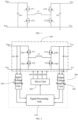
- control module 200 for a bidirectional DC converter. As shown in FIG. 2 , the control module 200 includes a signal processing unit 210 and a drive unit 220.
- the signal processing unit 210 is configured to determine an operating mode of the bidirectional DC converter according to an input voltage and an output voltage, and respectively determine a duty cycle of a drive signal VG1 of the first switch transistor VT1, a duty cycle of a drive signal VG2 of the second switch transistor VT2, a duty cycle of a drive signal VG3 of the third switch transistor VT3, and a duty cycle of a drive signal VG4 of the fourth switch transistor VT4 according to the operating mode of the bidirectional DC converter.
- the duty cycle of the drive signal VG1 of the first switch transistor VT1, the duty cycle of the drive signal VG2 of the second switch transistor VT2, the duty cycle of the drive signal VG3 of the third switch transistor VT3, and the duty cycle of the drive signal VG4 of the fourth switch transistor VT4 satisfy a following relationship:
- the drive unit 220 has at least one output terminal group, and each output terminal group includes a first output terminal electrically connected to a gate of the first switch transistor VT1, a second output terminal electrically connected to a gate of the second switch transistor VT2, a third output terminal electrically connected to a gate of the third switch transistor VT3, and a fourth output terminal electrically connected to a gate of the fourth switch transistor VT4.
- the drive unit 220 is configured to output the drive signal VG1 of the first switch transistor VT1 from the first output terminal according to the duty cycle of the drive signal VG1 of the first switch transistor VT1, output the drive signal VG2 of the second switch transistor VT2 from the second output terminal according to the duty cycle of the drive signal VG2 of the second switch transistor VT2, output the drive signal VG3 of the third switch transistor VT3 from the third output terminal according to the duty cycle of the drive signal VG3 of the third switch transistor VT3, and output the drive signal VG4 of the fourth switch transistor VT4 from the fourth output terminal according to the duty cycle of the drive signal VG4 of the fourth switch transistor VT4.
- the control module 200 is configured to perform the above control method provided by the present disclosure.
- the principles and beneficial effects of the control method have been described in detail above, and thus their detailed descriptions are omitted herein.
- control module further includes:
- the predetermined differential satisfies the following relation: 0 ⁇ ⁇ ⁇ 0.05 , where ⁇ represents the predetermined differential.
- the signal processing unit 210 determines the operating mode of the bidirectional DC converter to be the Buck mode.
- the signal processing unit 210 determines the operating mode of the bidirectional DC converter to be the Buck/Boost mode.
- the signal processing unit 210 determines the operating mode of the bidirectional DC converter to be the Boost mode.
- the signal processing unit 210 determines the operating mode of the bidirectional DC converter to be the Buck mode in response to Vo ⁇ K1' ⁇ Vin, where K1' represents a first hysteresis determination coefficient, and 0 ⁇ K1 ' ⁇ K1.
- the signal processing unit 210 determines the operating mode of the bidirectional DC converter to be the Buck/Boost mode in response to Vo ⁇ K2' ⁇ Vin, where K2' represents a second hysteresis determination coefficient, and 1 ⁇ K2' ⁇ K2.
- the bidirectional DC converter includes at least one power conversion unit 100 and the aforementioned control module 200 provided by the present disclosure.
- the power conversion unit 100 includes a first bridge arm, a second bridge arm, and an inductor L1.
- the first bridge arm includes a first switch transistor VT1 and a second switch transistor VT2, where a first electrode of the first switch transistor VT1 is electrically connected to a positive electrode Vin + of an input terminal of the bidirectional DC converter, a second electrode of the first switch transistor VT1 is electrically connected to a first electrode of the second switch transistor VT2, and a second electrode of the second switch transistor VT2 is electrically connected to a negative electrode Vin - of the input terminal of the bidirectional DC converter.
- the second bridge arm includes a third switch transistor VT3 and a fourth switch transistor VT4, where a first electrode of the third switch transistor VT3 is electrically connected to a negative electrode Vt - of an output terminal of the bidirectional DC converter, a second electrode of the third switch transistor VT3 is electrically connected to a first electrode of the fourth switch transistor VT4, and a second electrode of the fourth switch transistor VT4 is electrically connected to a positive electrode V + of the output terminal of the bidirectional DC converter.
- a first terminal of the inductor L1 is electrically connected to the second electrode of the first switch transistor VT1, and a second terminal of the inductor L1 is electrically connected to the first electrode of the fourth switch transistor VT4.
- number of the power output units 100 is not particularly limited.
- the bidirectional DC converter includes two power output units 100 connected in parallel.
- an input filter capacitor Cin may also be connected between the positive electrode of the input terminal and the negative electrode of the input terminal of the bidirectional DC converter
- an output filter capacitor Co may also be connected between the positive electrode of the output terminal and the negative electrode of the output terminal of the bidirectional DC converter.
- the switching frequencies of both the first bridge arm and the second bridge arm are set to be 25KHz.
- the Buck coefficient K1 is 0.95
- the Boost coefficient K2 is 1.05.
- the input voltage sampling unit 230 samples an input voltage signal and then sends it to the signal processing unit 210.
- the output voltage sampling unit 240 samples an output voltage signal and then sends it to the signal processing unit 210.
- the signal processing unit 210 receives input/output voltage sampling signals and makes comparison and determination.
- Vo ⁇ K1 ⁇ Vin the system determines Vo ⁇ Vin
- the power conversion unit 100 operates in the Buck mode, and the duty cycle of the switch transistor VT1 is set to D 1 .
- the signal processing unit 210 determines that the output voltage is relatively close to the input voltage at this moment, and further it is determined that that power conversion unit 100 is in the Buck/Boost mode.
- the duty cycle of the drive signal VG2 of the second switch transistor VT2 is set as D 22
- the output voltage is adjusted by adjusting the duty cycle D 2 of the drive signal VG3 of the third switch transistor VT3, thus 0.032 ⁇ D 22 ⁇ 0.124 in the Buck/Boost mode, and on-time of the third switch transistor VT3 is 1.28 ⁇ S ⁇ T ⁇ 4.96 ⁇ S.
- D 11 0.92
- D 1max 0.95
- the duty cycle of the drive signal VG1 of the first switch transistor VT1 does not change greatly during the transition from the Buck mode to the Buck/Boost mode.
- the drive signal VG4 of the fourth switch transistor VT4 starts to act at the same switching frequency as the first switch transistor VT1, and a high-level drive signal of the fourth switch transistor VT4 is centrosymmetrical with respect to a high-level signal of the first switch transistor VT1.
- a schematic waveform diagram of each drive signal in each mode is shown in FIG. 5 .
- the duty cycle (1-D 22 ) of the drive signal VG4 of the fourth switch transistor VT4 is reduced from 1 to the range of from 0.968 to 0.876 in the process of switching from the Buck mode to the Buck/Boost mode, such that a larger abrupt change in the duty cycle of the drive signal VG4 will not occur.
- the signal processing unit 210 determines that the output voltage is greater than the input voltage. At this moment, it is determined that the power output unit 100 operates in the Boost mode, and the first switch transistor VT1 is set to operate in the normal on state. At this moment, the duty cycle of the drive signal VG1 of the first switch transistor VT1 is 1, the second switch transistor VT2 is set to the normal off state, and the duty cycle of the drive signal VG2 of the second switch transistor VT2 is 0 at this moment.
- the input voltage is unchanged, and in the process of gradual rise of the output voltage, the duty cycle of each switch transistor is changed.
- the process of the output voltage gradually dropping from a high voltage is a reverse process of the above process, where the change of the duty cycle of each switch transistor a reverse change, which is a smooth transition and no larger abrupt change occurs, and thus is not described in detail here.
- hysteresis determination may be added at each switching point. Hysteresis setting is shown in FIG. 6 .
- a rising edge of the drive signal VG3 of the third switch transistor VT3 and a rising edge of the drive signal VG1 of the first switch transistor VT1 are generated at the same moment.
- a schematic waveform diagram of each drive signal in each mode in Embodiment 2 is shown in FIG. 7 .
- the range of the duty cycle of the drive signal VG3 of the third switch transistor VT3 in the Buck/Boost mode is: 1 ⁇ D 11 / 0.95 ⁇ D 22 ⁇ 1 ⁇ D 11 / 1.05 , i . e . , 0.074 ⁇ D 22 ⁇ 0.162 .
- the on-time of the third switch transistor VT3 in the Buck/Boost mode is 1.48 ⁇ S ⁇ T ⁇ 3.24 ⁇ S.
- the bidirectional DC converter in this embodiment includes two independent power output units 100, input terminals of the two power input units are connected in parallel, output terminals of the two power input units are connected in parallel, and a phase between the two power input units interleaves at an angle of 180 degrees.
- a computer-readable storage medium having an executable program stored thereon.
- the control method provided in the present disclosure can be implemented.
- control method provided by the present disclosure when used to control the bidirectional DC converter provided by the present disclosure, when the bidirectional DC converter is switched between operating modes, the duty cycle of the drive signal of each switch transistor can be avoided from changing to a larger extent, thereby avoiding the phenomenon of voltage offset.
- Such software may be distributed on a computer-readable medium, which may include a computer storage medium (or non-transitory medium) and a communication medium (or a transitory medium).
- computer storage media include volatile and nonvolatile, removable and non-removable media implemented in any method or technology for storage of information, such as computer-readable instructions, data structures, program modules, or other data.
- the computer storage media include, but are not limited to, RAM, ROM, EEPROM, flash memory or other memory technology, CD-ROM, digital versatile disks (DVD) or other optical storage, magnetic cassettes, magnetic tape, magnetic disk storage or other magnetic storage devices, or any other media which can be used to store the desired information and which can be accessed by a computer.
- communication media typically include computer-readable instructions, data structures, program modules or other data in a modulated data signal such as a carrier wave or other transport mechanism, and may include any information delivery media.
Landscapes
- Engineering & Computer Science (AREA)
- Power Engineering (AREA)
- Dc-Dc Converters (AREA)
Applications Claiming Priority (2)
| Application Number | Priority Date | Filing Date | Title |
|---|---|---|---|
| CN202010605231.0A CN113938008B (zh) | 2020-06-29 | 2020-06-29 | 双向dc变换器及其控制方法、控制模块、存储介质 |
| PCT/CN2021/102783 WO2022001966A1 (zh) | 2020-06-29 | 2021-06-28 | 双向dc变换器及其控制方法、控制模块、存储介质 |
Publications (2)
| Publication Number | Publication Date |
|---|---|
| EP4175147A1 true EP4175147A1 (de) | 2023-05-03 |
| EP4175147A4 EP4175147A4 (de) | 2023-11-29 |
Family
ID=79272913
Family Applications (1)
| Application Number | Title | Priority Date | Filing Date |
|---|---|---|---|
| EP21833767.3A Pending EP4175147A4 (de) | 2020-06-29 | 2021-06-28 | Bidirektionaler gleichstromwandler, steuerungsverfahren dafür und steuermodul dafür sowie speichermedium |
Country Status (6)
| Country | Link |
|---|---|
| US (1) | US12244232B2 (de) |
| EP (1) | EP4175147A4 (de) |
| JP (1) | JP7521017B2 (de) |
| CN (1) | CN113938008B (de) |
| WO (1) | WO2022001966A1 (de) |
| ZA (1) | ZA202301138B (de) |
Families Citing this family (9)
| Publication number | Priority date | Publication date | Assignee | Title |
|---|---|---|---|---|
| CN114744875A (zh) * | 2022-05-06 | 2022-07-12 | 长春捷翼汽车零部件有限公司 | 一种组合控制电压变换器、控制方法、电源和新能源汽车 |
| JP7818197B2 (ja) * | 2022-08-10 | 2026-02-20 | パナソニックIpマネジメント株式会社 | Dc/dcコンバータ、分散型電源システム |
| CN115224952B (zh) * | 2022-09-19 | 2023-01-17 | 如果新能源科技(江苏)股份有限公司 | 双向功率变换装置的控制方法及双向功率变换装置 |
| US20240113624A1 (en) * | 2022-09-30 | 2024-04-04 | Texas Instruments Incorporated | Multi-phase buck-boost converter |
| CN115765451A (zh) * | 2022-11-18 | 2023-03-07 | 瑞炬智能科技(天津)有限公司 | 电源模块的控制装置和方法 |
| CN116247936A (zh) * | 2023-02-09 | 2023-06-09 | 深圳市恩玖科技有限公司 | 基于双向升降压拓扑电路的控制方法 |
| GB2635521A (en) * | 2023-11-15 | 2025-05-21 | Nyobolt Ltd | Power controller |
| CN118232696B (zh) * | 2024-05-23 | 2024-07-26 | 西安图为电气技术有限公司 | 限流控制方法、电子设备及计算机可读存储介质 |
| CN120222805B (zh) * | 2025-03-27 | 2025-12-16 | 深圳市爱庞德新能源科技有限公司 | 一种具有电力载波通信的光伏电源适配器及光伏系统 |
Family Cites Families (19)
| Publication number | Priority date | Publication date | Assignee | Title |
|---|---|---|---|---|
| US7176667B2 (en) * | 2005-06-20 | 2007-02-13 | Aimtron Technology Corp. | Buck-boost voltage converter |
| CN101517877B (zh) * | 2006-09-15 | 2012-05-23 | 三菱电机株式会社 | Dc/dc电力转换装置 |
| US7804283B2 (en) * | 2007-08-14 | 2010-09-28 | Freescale Semiconductor, Inc. | Mode transitioning in a DC/DC converter using a constant duty cycle difference |
| KR100858028B1 (ko) * | 2008-04-17 | 2008-09-10 | 불루세라믹 주식회사 | 머리 미용기구 |
| JP5191270B2 (ja) | 2008-04-24 | 2013-05-08 | 川崎重工業株式会社 | デッドバンド補償方法および補償装置 |
| US7902807B2 (en) | 2008-07-22 | 2011-03-08 | Texas Instruments Incorporated | Multiple switch node power converter control scheme that avoids switching sub-harmonics |
| CN101499717B (zh) | 2009-02-17 | 2010-10-20 | 浙江大学 | 一种四开关升降压直流-直流变换器的控制方法及装置 |
| US8749215B2 (en) * | 2010-08-31 | 2014-06-10 | Texas Instruments Incorporated | Switching method to reduce ripple current in a switched-mode power converter employing a bridge topology |
| CN102857096A (zh) * | 2011-07-01 | 2013-01-02 | 上海康威特吉能源技术有限公司 | 一种升降压直流变换器控制方法 |
| US8841895B2 (en) * | 2012-06-04 | 2014-09-23 | Texas Instruments Deutschland Gmbh | Electronic device for average current mode DC-DC conversion |
| JP2015047040A (ja) * | 2013-08-29 | 2015-03-12 | 株式会社デンソー | スイッチング電源回路 |
| US10770893B2 (en) * | 2014-05-02 | 2020-09-08 | The Governing Council Of The University Of Toronto | Multi-port converter structure for DC/DC power conversion |
| US9802493B2 (en) | 2014-06-20 | 2017-10-31 | Cooper Technologies Company | Multi-phase bidirectional DC to DC power converter circuits, systems and methods with transient stress control |
| CN104821715B (zh) * | 2015-04-24 | 2017-05-17 | 成都芯源系统有限公司 | 升降压开关电路及其控制方法 |
| US10177661B2 (en) * | 2015-06-15 | 2019-01-08 | Futurewei Technologies, Inc. | Control method for buck-boost power converters |
| DE102015219850A1 (de) * | 2015-10-13 | 2017-04-13 | Fraunhofer-Gesellschaft zur Förderung der angewandten Forschung e.V. | Vorrichtung zum Steuern eines schaltenden Gleichspannungswandlers, schaltender Gleichspannungswandler und Verfahren zum Steuern eines geschalteten Gleichspannungswandlers |
| WO2018116699A1 (ja) | 2016-12-21 | 2018-06-28 | ソニー株式会社 | 電源回路および電動車両 |
| WO2020051557A1 (en) * | 2018-09-06 | 2020-03-12 | Cornell University | High power density power converter and uninterruptible power supply circuit and methods |
| CN109889047B (zh) * | 2019-01-31 | 2021-05-28 | 南京航空航天大学 | 一种适用于宽输入宽输出电压范围的两级式dc-dc变换器 |
-
2020
- 2020-06-29 CN CN202010605231.0A patent/CN113938008B/zh active Active
-
2021
- 2021-06-28 JP JP2022581495A patent/JP7521017B2/ja active Active
- 2021-06-28 WO PCT/CN2021/102783 patent/WO2022001966A1/zh not_active Ceased
- 2021-06-28 US US18/013,497 patent/US12244232B2/en active Active
- 2021-06-28 EP EP21833767.3A patent/EP4175147A4/de active Pending
-
2023
- 2023-01-27 ZA ZA2023/01138A patent/ZA202301138B/en unknown
Also Published As
| Publication number | Publication date |
|---|---|
| CN113938008B (zh) | 2023-12-22 |
| ZA202301138B (en) | 2024-09-25 |
| US12244232B2 (en) | 2025-03-04 |
| US20230344353A1 (en) | 2023-10-26 |
| JP7521017B2 (ja) | 2024-07-23 |
| JP2023533930A (ja) | 2023-08-07 |
| CN113938008A (zh) | 2022-01-14 |
| EP4175147A4 (de) | 2023-11-29 |
| WO2022001966A1 (zh) | 2022-01-06 |
Similar Documents
| Publication | Publication Date | Title |
|---|---|---|
| EP4175147A1 (de) | Bidirektionaler gleichstromwandler, steuerungsverfahren dafür und steuermodul dafür sowie speichermedium | |
| TWI477048B (zh) | 直流對直流轉換器及其電壓轉換方法 | |
| US11671015B2 (en) | Three-level boost circuit and multiple-output parallel system | |
| US11509227B2 (en) | Active clamp flyback converter | |
| US8502417B2 (en) | Power source device and output voltage changing method of the power source device | |
| US20150162829A1 (en) | Control Module of Constant On-Time Mode and Voltage Converting Device thereof | |
| US10116200B1 (en) | DC/DC converter device | |
| US20210050782A1 (en) | Switch-mode power supply with load current based throttling | |
| US20230058021A1 (en) | Circuits and method for reducing light load power dissipation of a voltage converter | |
| US12222378B2 (en) | Ripple detection device and ripple suppression device | |
| CN108649785A (zh) | SiC MOSFET三相两电平变换器死区设置方法 | |
| US20240072649A1 (en) | Totem-pole power factor correction circuit and power supply module | |
| US20240243667A1 (en) | Electric vehicle energy storage systems for mitigating transient load conditions in low voltage buses | |
| CN100355191C (zh) | 直流对直流转换器的控制电路、控制方法及时序产生器 | |
| CN118631045B (zh) | 一种死区时间控制电路、控制方法及电源 | |
| CN111049394B (zh) | 电源电路、电路控制方法、电源适配器、及电子设备 | |
| CN105591535B (zh) | 一种功率因数控制方法及装置 | |
| US8017256B2 (en) | Dual-power-supply system | |
| US10148110B2 (en) | Charging device and control method for controlling operations of different modulation modules according to load conditions | |
| EP4213357A1 (de) | Trägerfrequenzsteuerungsverfahren und -vorrichtung zur leistungsfaktorkorrektur und klimaanlage | |
| CN102082509B (zh) | 用于变频式电压调节器的频率控制电路及方法 | |
| US20260074601A1 (en) | Power supply conversion device | |
| TWI450483B (zh) | 直流對直流轉換器及其電壓轉換方法 | |
| US20250070638A1 (en) | Soft switch circuit and control method, and power source assembly | |
| US20250364886A1 (en) | Power supply controller and switching power supply |
Legal Events
| Date | Code | Title | Description |
|---|---|---|---|
| STAA | Information on the status of an ep patent application or granted ep patent |
Free format text: STATUS: THE INTERNATIONAL PUBLICATION HAS BEEN MADE |
|
| PUAI | Public reference made under article 153(3) epc to a published international application that has entered the european phase |
Free format text: ORIGINAL CODE: 0009012 |
|
| STAA | Information on the status of an ep patent application or granted ep patent |
Free format text: STATUS: REQUEST FOR EXAMINATION WAS MADE |
|
| 17P | Request for examination filed |
Effective date: 20230124 |
|
| AK | Designated contracting states |
Kind code of ref document: A1 Designated state(s): AL AT BE BG CH CY CZ DE DK EE ES FI FR GB GR HR HU IE IS IT LI LT LU LV MC MK MT NL NO PL PT RO RS SE SI SK SM TR |
|
| DAV | Request for validation of the european patent (deleted) | ||
| DAX | Request for extension of the european patent (deleted) | ||
| A4 | Supplementary search report drawn up and despatched |
Effective date: 20231031 |
|
| RIC1 | Information provided on ipc code assigned before grant |
Ipc: H02M 1/00 20060101ALI20231025BHEP Ipc: H02M 3/158 20060101AFI20231025BHEP |
|
| STAA | Information on the status of an ep patent application or granted ep patent |
Free format text: STATUS: EXAMINATION IS IN PROGRESS |
|
| 17Q | First examination report despatched |
Effective date: 20260129 |