EP4174940A2 - Esd-schutz auf paketniveau - Google Patents
Esd-schutz auf paketniveau Download PDFInfo
- Publication number
- EP4174940A2 EP4174940A2 EP22194221.2A EP22194221A EP4174940A2 EP 4174940 A2 EP4174940 A2 EP 4174940A2 EP 22194221 A EP22194221 A EP 22194221A EP 4174940 A2 EP4174940 A2 EP 4174940A2
- Authority
- EP
- European Patent Office
- Prior art keywords
- package
- esd
- pad
- component
- coupled
- Prior art date
- Legal status (The legal status is an assumption and is not a legal conclusion. Google has not performed a legal analysis and makes no representation as to the accuracy of the status listed.)
- Pending
Links
Images



Classifications
-
- H—ELECTRICITY
- H10—SEMICONDUCTOR DEVICES; ELECTRIC SOLID-STATE DEVICES NOT OTHERWISE PROVIDED FOR
- H10D—INORGANIC ELECTRIC SEMICONDUCTOR DEVICES
- H10D89/00—Aspects of integrated devices not covered by groups H10D84/00 - H10D88/00
- H10D89/60—Integrated devices comprising arrangements for electrical or thermal protection, e.g. protection circuits against electrostatic discharge [ESD]
- H10D89/601—Integrated devices comprising arrangements for electrical or thermal protection, e.g. protection circuits against electrostatic discharge [ESD] for devices having insulated gate electrodes, e.g. for IGFETs or IGBTs
- H10D89/921—Integrated devices comprising arrangements for electrical or thermal protection, e.g. protection circuits against electrostatic discharge [ESD] for devices having insulated gate electrodes, e.g. for IGFETs or IGBTs characterised by the configuration of the interconnections connecting the protective arrangements, e.g. ESD buses
-
- H—ELECTRICITY
- H10—SEMICONDUCTOR DEVICES; ELECTRIC SOLID-STATE DEVICES NOT OTHERWISE PROVIDED FOR
- H10W—GENERIC PACKAGES, INTERCONNECTIONS, CONNECTORS OR OTHER CONSTRUCTIONAL DETAILS OF DEVICES COVERED BY CLASS H10
- H10W42/00—Arrangements for protection of devices
- H10W42/60—Arrangements for protection of devices protecting against electrostatic charges or discharges, e.g. Faraday shields
-
- H—ELECTRICITY
- H10—SEMICONDUCTOR DEVICES; ELECTRIC SOLID-STATE DEVICES NOT OTHERWISE PROVIDED FOR
- H10W—GENERIC PACKAGES, INTERCONNECTIONS, CONNECTORS OR OTHER CONSTRUCTIONAL DETAILS OF DEVICES COVERED BY CLASS H10
- H10W72/00—Interconnections or connectors in packages
- H10W72/20—Bump connectors, e.g. solder bumps or copper pillars; Dummy bumps; Thermal bumps
-
- H—ELECTRICITY
- H10—SEMICONDUCTOR DEVICES; ELECTRIC SOLID-STATE DEVICES NOT OTHERWISE PROVIDED FOR
- H10W—GENERIC PACKAGES, INTERCONNECTIONS, CONNECTORS OR OTHER CONSTRUCTIONAL DETAILS OF DEVICES COVERED BY CLASS H10
- H10W74/00—Encapsulations, e.g. protective coatings
- H10W74/10—Encapsulations, e.g. protective coatings characterised by their shape or disposition
- H10W74/111—Encapsulations, e.g. protective coatings characterised by their shape or disposition the semiconductor body being completely enclosed
- H10W74/114—Encapsulations, e.g. protective coatings characterised by their shape or disposition the semiconductor body being completely enclosed by a substrate and the encapsulations
- H10W74/117—Encapsulations, e.g. protective coatings characterised by their shape or disposition the semiconductor body being completely enclosed by a substrate and the encapsulations the substrate having spherical bumps for external connection
-
- H—ELECTRICITY
- H10—SEMICONDUCTOR DEVICES; ELECTRIC SOLID-STATE DEVICES NOT OTHERWISE PROVIDED FOR
- H10W—GENERIC PACKAGES, INTERCONNECTIONS, CONNECTORS OR OTHER CONSTRUCTIONAL DETAILS OF DEVICES COVERED BY CLASS H10
- H10W90/00—Package configurations
- H10W90/701—Package configurations characterised by the relative positions of pads or connectors relative to package parts
-
- H—ELECTRICITY
- H10—SEMICONDUCTOR DEVICES; ELECTRIC SOLID-STATE DEVICES NOT OTHERWISE PROVIDED FOR
- H10W—GENERIC PACKAGES, INTERCONNECTIONS, CONNECTORS OR OTHER CONSTRUCTIONAL DETAILS OF DEVICES COVERED BY CLASS H10
- H10W44/00—Electrical arrangements for controlling or matching impedance
- H10W44/20—Electrical arrangements for controlling or matching impedance at high-frequency [HF] or radio frequency [RF]
Definitions
- one or more ESD protection circuits are designed within the die to pass a human body model (HBM) and charged device model (CDM) of ESD specifications.
- HBM human body model
- CDM charged device model
- the die-level ESD protection circuits generally have higher parasitic effects; and if the die-level ESD protection circuits are designed with smaller size to lower the parasitic effects, the die-level ESD protection circuits will not have good ESD robustness for high-speed radio-frequency (RF) designs.
- RF radio-frequency
- a package comprising a first pad, a die and at least one package ESD component.
- the first pad is configured to receive a signal from a device external to the package or transmit a signal from an internal circuit to the device external to the package.
- the die comprises a second pad and the internal circuit, wherein the internal circuit is configured to receive the signal from the first pad via the second pad or transmit the signal from the internal circuit to the first pad via the second pad.
- the at least one ESD component is positioned outside the die.
- FIG. 1 is a diagram illustrating a package 100 according to one embodiment of the present invention, wherein the package 100 can be any integrated circuit (IC) package such as chip-on-wafer-on-substrate (CoWoS), integrated fan out (InFO) or any other two-dimensional IC package or three-dimensional IC package.
- the package 100 comprises a die 110, a package ESD conducting component 120, a package ESD conducting component 130, a package ESD blocking component 140 and a plurality of pads (a pad N1 serves as an example), wherein the die 110 comprises a plurality of pads (a pad N2 serves as an example), an internal circuit 112, a die ESD component 114 and a die ESD component 116.
- IC integrated circuit
- CoWoS chip-on-wafer-on-substrate
- InFO integrated fan out
- the package 100 comprises a die 110, a package ESD conducting component 120, a package ESD conducting component 130, a package ESD blocking component 140 and a
- the pad N1 may be a pin or one of a ball grid array (BGA), and the pad N1 is used to receive a signal from a device outside the package 100, or the pad N1 is used to transmit a signal from the internal circuit 112 to the device outside the package 100.
- the package ESD conducting component 120 is coupled between a supply voltage VDD and the pad N1
- the package ESD conducting component 130 connected between a ground voltage and the pad N1
- the package ESD blocking component 140 is coupled between the pad N1 and the pad N2.
- the die ESD component is coupled between the supply voltage VDD and the pad N2
- the die ESD component is coupled between the ground voltage and the pad N2
- the internal circuit 112 is configured to receive and process the signal from the pad N1 via the package ESD blocking component 140 and the pad N2.
- three package ESD components are designed within the package 100 to protect the internal circuit 112 against the ESD damage, however, the number and type of package ESD components are not limitations of the present invention.
- one or two of the package ESD conducting component 120, the package ESD conducting component 130 and the package ESD blocking component 140 can be removed from the package 100.
- the package ESD components between the pad N1 and the die 110 By designing the package ESD components between the pad N1 and the die 110, most of the ESD current can be bypassed by the package ESD conducting component 130 or blocked by the package ESD blocking component 140, so the remaining ESD current flowing into the die 110 will only induce small voltage drop, and package 100 can meet the requirements of the ESD specifications for high-speed RF designs. In addition, because the package ESD components with lower parasitic effects have better quality factor control and ESD robustness, the package 100 with the package ESD components will have better performance.
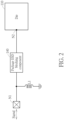
- FIG. 2 is a diagram illustrating the package ESD components according to a first embodiment of the present invention.
- the package 100 comprises the package ESD conducting component 130 and the package ESD blocking component 140, wherein the package ESD conducting component 130 is implemented by using an inductor L1, that is one node of the inductor L1 is coupled to the pad N1, and the other node of the inductor L1 is coupled to the ground voltage.
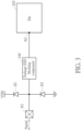
- FIG. 3 is a diagram illustrating the package ESD components according to a second embodiment of the present invention.
- the package 100 comprises the package ESD conducting component 120, the package ESD conducting component 130 and the package ESD blocking component 140.
- the package ESD conducting component 120 is implemented by using a diode D1, wherein an anode of the diode D1 is coupled to the pad N1, and a cathode of the diode D1 is coupled to the supply voltage VDD.
- the package ESD conducting component 130 is implemented by using a diode D2, wherein an anode of the diode D2 is coupled to the ground voltage, and a cathode of the diode D2 is coupled to the pad N1.
- FIG. 4 is a diagram illustrating the package ESD components according to a third embodiment of the present invention.
- the package 100 comprises the package ESD conducting component 120, the package ESD conducting component 130 and the package ESD blocking component 140.
- the package ESD conducting component 120 is implemented by using a P-type transistor MP1, wherein a source electrode of the P-type transistor MP1 is coupled to the supply voltage VDD, and a drain electrode of the P-type transistor MP1 is coupled to the pad N1.
- the package ESD conducting component 130 is implemented by using an N-type transistor MN1, wherein a source electrode of the N-type transistor MN1 is coupled to the ground voltage, and a drain electrode of the N-type transistor MN1 is coupled to the pad N1.
- FIG. 5 is a diagram illustrating the package ESD components according to a fourth embodiment of the present invention.
- the package 100 comprises the package ESD conducting component 130 and the package ESD blocking component 140.
- the package ESD conducting component 130 is implemented by using forward diode (s) D4 and D5 and reverse diode (s) D3.
- An anode of the diode D3 is coupled to the ground voltage, and a cathode of the diode D3 is coupled to the pad N1.
- the diodes D4 and D5 are connected in series, wherein an anode of the diode D4 is coupled to the pad N1, and a cathode of the diode D5 is coupled to the ground voltage.
- FIG. 6 is a diagram illustrating the package ESD components according to a fifth embodiment of the present invention.
- the package 100 comprises the package ESD conducting component 130 and the package ESD blocking component 140.
- the package ESD conducting component 130 is implemented by using an inductor L2 and a capacitor C1 connected in series, wherein a first node of the inductor L2 is coupled to the pad N1, a second node of the inductor L2 is coupled to a first node of the capacitor C1, and a second node of the capacitor C1 is coupled to the ground voltage.
- FIG. 7 is a diagram illustrating the package ESD components according to a sixth embodiment of the present invention.
- the package 100 comprises the package ESD conducting component 130 and the package ESD blocking component 140.
- the package ESD conducting component 130 is implemented by using an inductor L3 and a capacitor C2 connected in parallel, wherein a first node of the inductor L3 is coupled to the pad N1, a second node of the inductor L3 is coupled to the ground voltage, a first node of the capacitor C2 is coupled to the pad N1, a second node of the capacitor C2 is coupled to the ground voltage.
- FIG. 8 is a diagram illustrating the package ESD components according to a seventh embodiment of the present invention.
- the package 100 comprises the package ESD conducting component 130 and the package ESD blocking component 140.
- the package ESD conducting component 130 is implemented by using an inductor L4, forward diode (s) D7 and D8 and reverse diode (s) D6.
- a first node of the inductor L4 is coupled to the pad N1
- an anode of the diode D3 is coupled to the ground voltage
- a cathode of the diode D3 is coupled to a second node of the inductor L4.
- the diodes D4 and D5 are connected in series, wherein an anode of the diode D4 is coupled to the second node of the inductor L4, and a cathode of the diode D5 is coupled to the ground voltage.
- FIG. 9 is a diagram showing some embodiments of the package ESD blocking component 140 coupled between the pad N1 and the pad N2.
- the package ESD blocking component 140 can be implemented by using a resistor R1, an inductor L5 or a capacitor C3, wherein a first node of the resistor R1, the inductor L5 or the capacitor C3 is coupled to the pad N1, and a second node of the resistor R1, the inductor L5 or the capacitor C3 is coupled to the pad N2.
- FIG. 10 is a diagram showing some embodiments of the package ESD blocking component 140 coupled between the pad N1 and the pad N2.
- the package ESD blocking component 140 can be implemented by using via hole, wherein the via hole is manufactured by a plurality of metal layers.
- the package ESD blocking component 140 can be implemented by using an inductor L6 and a capacitor C4 connected in series, wherein a first node of the inductor L6 is coupled to the pad N1, a second node of the inductor L6 is coupled to a firs node of the capacitor C4, and a second node of the capacitor C4 is coupled to the pad N2.
- the package ESD blocking component 140 can be implemented by using an inductor L7 and a capacitor C5 connected in parallel, wherein a first node of the inductor L7 is coupled to the pad N1, a second node of the inductor L7 is coupled to the pad N2, a first node of the capacitor C5 is coupled to the pad N1, and a second node of the capacitor C5 is coupled to the pad N2.
- the package ESD conducting component 130 can be implemented by using the inductor L1 shown in FIG. 2 to bypass the ESD current.
- the ESD frequency is within a lower frequency range
- a frequency of required signal is within a higher frequency range
- the inductor L1 serves as a high-pass filter to bypass the ESD current to the ground
- the high-frequency component can enter the pad N2 of the die 110.
- the die ESD component 116 within the die 110 can also be implemented by using an inductor L8, to bypass the remaining ESD current to the ground.
- the die comprises an RF circuit for processing a millimeter wave (mmW) signal
- the ESD frequency may be ranging from 100 MHz to 6GHz
- a frequency of the required millimeter wave signal is ranging from 24 GHz to 40 GHz.
- the inductor L1 can have different designs for different frequencies.
- the inductor L1 when the pad N1 is used to receive or transmit the millimeter wave signal with 28 GHz, the inductor L1 can be formed by using a sixth metal layer having the ground voltage around a BGA ball; and when the pad N1 is used to receive or transmit the millimeter wave signal with 39 GHz, the inductor L1 can be formed by using a fifth metal layer in keep-out zone.
- FIG. 13 is a diagram illustrating a vertical cross-sectional view of the circuit connected to the BGA ball.
- the circuits comprise a first component 1302 and a second component 1304, wherein the first component 1302 can be the package ESD conducting component formed by using the fifth metal layer L5 and the sixth metal layer 6, and the second component 1304 can be the package ESD blocking component formed by using a first metal layer to a fourth metal layer L1 - L4.
- the embodiments of the present invention by designing one or more package-level ESD component(s) between the die and the pad(s) of the package, most of the ESD current can be bypassed outside the die, and the remaining ESD current flowing into the die will only induce small voltage drop.
- the package ESD components with lower parasitic effects have better quality factor control and ESD robustness, the package with the package ESD components will have better performance.
Landscapes
- Semiconductor Integrated Circuits (AREA)
- Engineering & Computer Science (AREA)
- Power Engineering (AREA)
Applications Claiming Priority (2)
| Application Number | Priority Date | Filing Date | Title |
|---|---|---|---|
| US202163274032P | 2021-11-01 | 2021-11-01 | |
| US17/902,912 US12564063B2 (en) | 2021-11-01 | 2022-09-05 | Package-level ESD protection |
Publications (2)
| Publication Number | Publication Date |
|---|---|
| EP4174940A2 true EP4174940A2 (de) | 2023-05-03 |
| EP4174940A3 EP4174940A3 (de) | 2023-07-05 |
Family
ID=83228829
Family Applications (1)
| Application Number | Title | Priority Date | Filing Date |
|---|---|---|---|
| EP22194221.2A Pending EP4174940A3 (de) | 2021-11-01 | 2022-09-06 | Esd-schutz auf paketniveau |
Country Status (4)
| Country | Link |
|---|---|
| US (2) | US12564063B2 (de) |
| EP (1) | EP4174940A3 (de) |
| CN (1) | CN116072668A (de) |
| TW (1) | TWI833386B (de) |
Family Cites Families (24)
| Publication number | Priority date | Publication date | Assignee | Title |
|---|---|---|---|---|
| US6208493B1 (en) | 1993-09-13 | 2001-03-27 | Texas Instruments Incorporated | Method and system for protecting integrated circuits against a variety of transients |
| KR100223888B1 (ko) | 1996-11-20 | 1999-10-15 | 구본준 | 정전기 보호회로 |
| US6586266B1 (en) * | 1999-03-01 | 2003-07-01 | Megic Corporation | High performance sub-system design and assembly |
| TWI240403B (en) | 2004-04-29 | 2005-09-21 | Via Tech Inc | Electrostatic discharge protection circuit |
| US20060250731A1 (en) | 2005-05-03 | 2006-11-09 | Parkhurst Ray M | System and method for electrostatic discharge protection in an electronic circuit |
| US7894173B2 (en) * | 2008-09-16 | 2011-02-22 | Taiwan Semiconductor Manufacturing Company, Ltd. | Enhancing bandwidth of ESD network using transformers |
| US8723257B2 (en) | 2008-12-15 | 2014-05-13 | United Microelectronics Corp. | ESD protection device having reduced equivalent capacitance |
| US8183593B2 (en) | 2009-10-16 | 2012-05-22 | Oracle America, Inc. | Semiconductor die with integrated electro-static discharge device |
| US8181140B2 (en) * | 2009-11-09 | 2012-05-15 | Xilinx, Inc. | T-coil network design for improved bandwidth and electrostatic discharge immunity |
| US9224728B2 (en) * | 2010-02-26 | 2015-12-29 | Littelfuse, Inc. | Embedded protection against spurious electrical events |
| EP2577716A1 (de) | 2010-05-24 | 2013-04-10 | Shocking Technologies Inc | Schaltkreiselemente mit ferroischen materialien |
| TW201214653A (en) | 2010-09-23 | 2012-04-01 | Siliconware Precision Industries Co Ltd | Package structure capable of discharging static electricity and preventing electromagnetic wave interference |
| US8854777B2 (en) * | 2010-11-05 | 2014-10-07 | Avago Technologies General Ip (Singapore) Pte. Ltd. | Systems and methods for ESD protection for RF couplers in semiconductor packages |
| US8504952B2 (en) | 2010-12-28 | 2013-08-06 | Wilocity, Ltd. | Electrostatic discharge (ESD) protection circuit and method for designing thereof for protection of millimeter wave electrical elements |
| US9460840B2 (en) | 2011-03-03 | 2016-10-04 | Skyworks Solutions, Inc. | Seal ring inductor and method of forming the same |
| US20150188312A1 (en) | 2013-12-27 | 2015-07-02 | Cambridge Silicon Radio Limited | Electrostatic discharge protection |
| US9601920B2 (en) | 2014-07-10 | 2017-03-21 | Infineon Technologies Ag | Transient voltage protection circuits and devices |
| EP3007232A1 (de) | 2014-10-08 | 2016-04-13 | Nxp B.V. | Schutzvorrichtung für elektrostatische Entladung |
| US9853446B2 (en) * | 2015-08-27 | 2017-12-26 | Qualcomm Incorporated | Integrated circuit (IC) package comprising electrostatic discharge (ESD) protection |
| US10446541B2 (en) | 2015-09-14 | 2019-10-15 | Intel IP Corporation | Advanced node cost reduction by ESD interposer |
| JP6384644B2 (ja) * | 2016-08-01 | 2018-09-05 | 株式会社村田製作所 | Esd保護機能付きフィルタ部品 |
| WO2018179086A1 (ja) * | 2017-03-28 | 2018-10-04 | 三菱電機株式会社 | 半導体装置 |
| US10868421B2 (en) | 2018-07-05 | 2020-12-15 | Amazing Microelectronic Corp. | On-chip multiple-stage electrical overstress (EOS) protection device |
| JP2020013632A (ja) | 2018-07-13 | 2020-01-23 | 富士通コンポーネント株式会社 | 高周波モジュール |
-
2022
- 2022-09-05 US US17/902,912 patent/US12564063B2/en active Active
- 2022-09-06 EP EP22194221.2A patent/EP4174940A3/de active Pending
- 2022-10-11 CN CN202211243385.5A patent/CN116072668A/zh active Pending
- 2022-10-13 TW TW111138756A patent/TWI833386B/zh active
-
2025
- 2025-09-01 US US19/315,811 patent/US20250391791A1/en active Pending
Also Published As
| Publication number | Publication date |
|---|---|
| TWI833386B (zh) | 2024-02-21 |
| EP4174940A3 (de) | 2023-07-05 |
| US12564063B2 (en) | 2026-02-24 |
| US20250391791A1 (en) | 2025-12-25 |
| TW202320267A (zh) | 2023-05-16 |
| CN116072668A (zh) | 2023-05-05 |
| US20230138324A1 (en) | 2023-05-04 |
Similar Documents
| Publication | Publication Date | Title |
|---|---|---|
| US5721656A (en) | Electrostatc discharge protection network | |
| US7804671B2 (en) | Electrostatic discharge protection circuit | |
| US8324658B2 (en) | ESD protection circuit for RFID tag | |
| US7067914B2 (en) | Dual chip stack method for electro-static discharge protection of integrated circuits | |
| US8723257B2 (en) | ESD protection device having reduced equivalent capacitance | |
| US20070296055A1 (en) | Rf integrated circuit with esd protection and esd protection apparatus thereof | |
| US20120176708A1 (en) | Esd protection devices and methods for forming esd protection devices | |
| US8861149B2 (en) | ESD protection devices and methods for forming ESD protection devices | |
| EP0976190A1 (de) | Verteilter esd-schutz für hochgeschwindigkeitsintegrierte schaltungen | |
| CN112420688B (zh) | 一种静电保护电路 | |
| US6815821B2 (en) | Method of fabricating seal-ring structure with ESD protection | |
| US9224702B2 (en) | Three-dimension (3D) integrated circuit (IC) package | |
| JP2005217043A (ja) | 静電破壊保護回路 | |
| Chen et al. | On-chip HBM and HMM ESD protection design for RF applications in 40-nm CMOS process | |
| Lin | Review of Low-C ESD Protection Designs for High-Speed and High-Frequency Applications | |
| US10833064B2 (en) | ESD protection circuit and integrated circuit for broadband circuit | |
| US20110168782A1 (en) | Capacitance under a fringe capacitor of a radio frquency integrated circuit | |
| US10388647B1 (en) | Transient voltage suppression device | |
| EP1359620A2 (de) | ESD-Schutz für rauschentkopplende Kondensatoren | |
| US20060274465A1 (en) | Electrostatic discharge (ESD) protection circuits using metal-insulator-metal (MIM) capacitors | |
| EP3457435B1 (de) | Schutzstruktur gegen elektrostatische entladung | |
| US12564063B2 (en) | Package-level ESD protection | |
| US20170338219A1 (en) | Semiconductor integrated circuit device including an electrostatic discharge protection circuit | |
| US20040262689A1 (en) | Electrostatic discharge protection circuit | |
| US8605396B2 (en) | ESD protection devices and methods for forming ESD protection devices |
Legal Events
| Date | Code | Title | Description |
|---|---|---|---|
| PUAI | Public reference made under article 153(3) epc to a published international application that has entered the european phase |
Free format text: ORIGINAL CODE: 0009012 |
|
| STAA | Information on the status of an ep patent application or granted ep patent |
Free format text: STATUS: THE APPLICATION HAS BEEN PUBLISHED |
|
| AK | Designated contracting states |
Kind code of ref document: A2 Designated state(s): AL AT BE BG CH CY CZ DE DK EE ES FI FR GB GR HR HU IE IS IT LI LT LU LV MC MK MT NL NO PL PT RO RS SE SI SK SM TR |
|
| PUAL | Search report despatched |
Free format text: ORIGINAL CODE: 0009013 |
|
| AK | Designated contracting states |
Kind code of ref document: A3 Designated state(s): AL AT BE BG CH CY CZ DE DK EE ES FI FR GB GR HR HU IE IS IT LI LT LU LV MC MK MT NL NO PL PT RO RS SE SI SK SM TR |
|
| RIC1 | Information provided on ipc code assigned before grant |
Ipc: H01L 23/66 20060101ALN20230601BHEP Ipc: H01L 23/60 20060101AFI20230601BHEP |
|
| STAA | Information on the status of an ep patent application or granted ep patent |
Free format text: STATUS: REQUEST FOR EXAMINATION WAS MADE |
|
| 17P | Request for examination filed |
Effective date: 20240103 |
|
| RBV | Designated contracting states (corrected) |
Designated state(s): AL AT BE BG CH CY CZ DE DK EE ES FI FR GB GR HR HU IE IS IT LI LT LU LV MC MK MT NL NO PL PT RO RS SE SI SK SM TR |
|
| STAA | Information on the status of an ep patent application or granted ep patent |
Free format text: STATUS: EXAMINATION IS IN PROGRESS |