EP4174370A1 - Light source unit for vehicle lamp, vehicle lamp - Google Patents
Light source unit for vehicle lamp, vehicle lamp Download PDFInfo
- Publication number
- EP4174370A1 EP4174370A1 EP21834182.4A EP21834182A EP4174370A1 EP 4174370 A1 EP4174370 A1 EP 4174370A1 EP 21834182 A EP21834182 A EP 21834182A EP 4174370 A1 EP4174370 A1 EP 4174370A1
- Authority
- EP
- European Patent Office
- Prior art keywords
- substrate
- light source
- vehicle lamp
- semiconductor light
- source unit
- Prior art date
- Legal status (The legal status is an assumption and is not a legal conclusion. Google has not performed a legal analysis and makes no representation as to the accuracy of the status listed.)
- Granted
Links
Images




Classifications
-
- B—PERFORMING OPERATIONS; TRANSPORTING
- B60—VEHICLES IN GENERAL
- B60Q—ARRANGEMENT OF SIGNALLING OR LIGHTING DEVICES, THE MOUNTING OR SUPPORTING THEREOF OR CIRCUITS THEREFOR, FOR VEHICLES IN GENERAL
- B60Q1/00—Arrangement of optical signalling or lighting devices, the mounting or supporting thereof or circuits therefor
- B60Q1/0088—Details of electrical connections
- B60Q1/0094—Arrangement of electronic circuits separated from the light source, e.g. mounting of housings for starter circuits for discharge lamps
-
- F—MECHANICAL ENGINEERING; LIGHTING; HEATING; WEAPONS; BLASTING
- F21—LIGHTING
- F21S—NON-PORTABLE LIGHTING DEVICES; SYSTEMS THEREOF; VEHICLE LIGHTING DEVICES SPECIALLY ADAPTED FOR VEHICLE EXTERIORS
- F21S41/00—Illuminating devices specially adapted for vehicle exteriors, e.g. headlamps
- F21S41/10—Illuminating devices specially adapted for vehicle exteriors, e.g. headlamps characterised by the light source
- F21S41/19—Attachment of light sources or lamp holders
-
- F—MECHANICAL ENGINEERING; LIGHTING; HEATING; WEAPONS; BLASTING
- F21—LIGHTING
- F21K—NON-ELECTRIC LIGHT SOURCES USING LUMINESCENCE; LIGHT SOURCES USING ELECTROCHEMILUMINESCENCE; LIGHT SOURCES USING CHARGES OF COMBUSTIBLE MATERIAL; LIGHT SOURCES USING SEMICONDUCTOR DEVICES AS LIGHT-GENERATING ELEMENTS; LIGHT SOURCES NOT OTHERWISE PROVIDED FOR
- F21K9/00—Light sources using semiconductor devices as light-generating elements, e.g. using light-emitting diodes [LED] or lasers
- F21K9/20—Light sources comprising attachment means
- F21K9/23—Retrofit light sources for lighting devices with a single fitting for each light source, e.g. for substitution of incandescent lamps with bayonet or threaded fittings
-
- F—MECHANICAL ENGINEERING; LIGHTING; HEATING; WEAPONS; BLASTING
- F21—LIGHTING
- F21S—NON-PORTABLE LIGHTING DEVICES; SYSTEMS THEREOF; VEHICLE LIGHTING DEVICES SPECIALLY ADAPTED FOR VEHICLE EXTERIORS
- F21S41/00—Illuminating devices specially adapted for vehicle exteriors, e.g. headlamps
- F21S41/10—Illuminating devices specially adapted for vehicle exteriors, e.g. headlamps characterised by the light source
- F21S41/14—Illuminating devices specially adapted for vehicle exteriors, e.g. headlamps characterised by the light source characterised by the type of light source
- F21S41/141—Light emitting diodes [LED]
- F21S41/143—Light emitting diodes [LED] the main emission direction of the LED being parallel to the optical axis of the illuminating device
-
- F—MECHANICAL ENGINEERING; LIGHTING; HEATING; WEAPONS; BLASTING
- F21—LIGHTING
- F21S—NON-PORTABLE LIGHTING DEVICES; SYSTEMS THEREOF; VEHICLE LIGHTING DEVICES SPECIALLY ADAPTED FOR VEHICLE EXTERIORS
- F21S41/00—Illuminating devices specially adapted for vehicle exteriors, e.g. headlamps
- F21S41/10—Illuminating devices specially adapted for vehicle exteriors, e.g. headlamps characterised by the light source
- F21S41/19—Attachment of light sources or lamp holders
- F21S41/192—Details of lamp holders, terminals or connectors
-
- F—MECHANICAL ENGINEERING; LIGHTING; HEATING; WEAPONS; BLASTING
- F21—LIGHTING
- F21S—NON-PORTABLE LIGHTING DEVICES; SYSTEMS THEREOF; VEHICLE LIGHTING DEVICES SPECIALLY ADAPTED FOR VEHICLE EXTERIORS
- F21S41/00—Illuminating devices specially adapted for vehicle exteriors, e.g. headlamps
- F21S41/10—Illuminating devices specially adapted for vehicle exteriors, e.g. headlamps characterised by the light source
- F21S41/19—Attachment of light sources or lamp holders
- F21S41/194—Bayonet attachments
-
- F—MECHANICAL ENGINEERING; LIGHTING; HEATING; WEAPONS; BLASTING
- F21—LIGHTING
- F21S—NON-PORTABLE LIGHTING DEVICES; SYSTEMS THEREOF; VEHICLE LIGHTING DEVICES SPECIALLY ADAPTED FOR VEHICLE EXTERIORS
- F21S43/00—Signalling devices specially adapted for vehicle exteriors, e.g. brake lamps, direction indicator lights or reversing lights
- F21S43/10—Signalling devices specially adapted for vehicle exteriors, e.g. brake lamps, direction indicator lights or reversing lights characterised by the light source
- F21S43/13—Signalling devices specially adapted for vehicle exteriors, e.g. brake lamps, direction indicator lights or reversing lights characterised by the light source characterised by the type of light source
- F21S43/14—Light emitting diodes [LED]
-
- F—MECHANICAL ENGINEERING; LIGHTING; HEATING; WEAPONS; BLASTING
- F21—LIGHTING
- F21S—NON-PORTABLE LIGHTING DEVICES; SYSTEMS THEREOF; VEHICLE LIGHTING DEVICES SPECIALLY ADAPTED FOR VEHICLE EXTERIORS
- F21S43/00—Signalling devices specially adapted for vehicle exteriors, e.g. brake lamps, direction indicator lights or reversing lights
- F21S43/10—Signalling devices specially adapted for vehicle exteriors, e.g. brake lamps, direction indicator lights or reversing lights characterised by the light source
- F21S43/19—Attachment of light sources or lamp holders
- F21S43/195—Details of lamp holders, terminals or connectors
-
- F—MECHANICAL ENGINEERING; LIGHTING; HEATING; WEAPONS; BLASTING
- F21—LIGHTING
- F21S—NON-PORTABLE LIGHTING DEVICES; SYSTEMS THEREOF; VEHICLE LIGHTING DEVICES SPECIALLY ADAPTED FOR VEHICLE EXTERIORS
- F21S43/00—Signalling devices specially adapted for vehicle exteriors, e.g. brake lamps, direction indicator lights or reversing lights
- F21S43/20—Signalling devices specially adapted for vehicle exteriors, e.g. brake lamps, direction indicator lights or reversing lights characterised by refractors, transparent cover plates, light guides or filters
- F21S43/26—Refractors, transparent cover plates, light guides or filters not provided in groups F21S43/235 - F21S43/255
-
- F—MECHANICAL ENGINEERING; LIGHTING; HEATING; WEAPONS; BLASTING
- F21—LIGHTING
- F21S—NON-PORTABLE LIGHTING DEVICES; SYSTEMS THEREOF; VEHICLE LIGHTING DEVICES SPECIALLY ADAPTED FOR VEHICLE EXTERIORS
- F21S43/00—Signalling devices specially adapted for vehicle exteriors, e.g. brake lamps, direction indicator lights or reversing lights
- F21S43/20—Signalling devices specially adapted for vehicle exteriors, e.g. brake lamps, direction indicator lights or reversing lights characterised by refractors, transparent cover plates, light guides or filters
- F21S43/281—Materials thereof; Structures thereof; Properties thereof; Coatings thereof
- F21S43/28131—Structures comprising multiple layers
-
- F—MECHANICAL ENGINEERING; LIGHTING; HEATING; WEAPONS; BLASTING
- F21—LIGHTING
- F21S—NON-PORTABLE LIGHTING DEVICES; SYSTEMS THEREOF; VEHICLE LIGHTING DEVICES SPECIALLY ADAPTED FOR VEHICLE EXTERIORS
- F21S45/00—Arrangements within vehicle lighting devices specially adapted for vehicle exteriors, for purposes other than emission or distribution of light
-
- F—MECHANICAL ENGINEERING; LIGHTING; HEATING; WEAPONS; BLASTING
- F21—LIGHTING
- F21S—NON-PORTABLE LIGHTING DEVICES; SYSTEMS THEREOF; VEHICLE LIGHTING DEVICES SPECIALLY ADAPTED FOR VEHICLE EXTERIORS
- F21S45/00—Arrangements within vehicle lighting devices specially adapted for vehicle exteriors, for purposes other than emission or distribution of light
- F21S45/40—Cooling of lighting devices
- F21S45/47—Passive cooling, e.g. using fins, thermal conductive elements or openings
- F21S45/48—Passive cooling, e.g. using fins, thermal conductive elements or openings with means for conducting heat from the inside to the outside of the lighting devices, e.g. with fins on the outer surface of the lighting device
-
- B—PERFORMING OPERATIONS; TRANSPORTING
- B60—VEHICLES IN GENERAL
- B60Q—ARRANGEMENT OF SIGNALLING OR LIGHTING DEVICES, THE MOUNTING OR SUPPORTING THEREOF OR CIRCUITS THEREFOR, FOR VEHICLES IN GENERAL
- B60Q1/00—Arrangement of optical signalling or lighting devices, the mounting or supporting thereof or circuits therefor
- B60Q1/0088—Details of electrical connections
-
- F—MECHANICAL ENGINEERING; LIGHTING; HEATING; WEAPONS; BLASTING
- F21—LIGHTING
- F21Y—INDEXING SCHEME ASSOCIATED WITH SUBCLASSES F21K, F21L, F21S and F21V, RELATING TO THE FORM OR THE KIND OF THE LIGHT SOURCES OR OF THE COLOUR OF THE LIGHT EMITTED
- F21Y2115/00—Light-generating elements of semiconductor light sources
- F21Y2115/10—Light-emitting diodes [LED]
Definitions
- the present invention relates to a light source unit for a vehicle lamp, and a vehicle lamp.
- PTL 1 As a light source unit for a vehicle lamp and a vehicle lamp, in which a semiconductor light-emitting element and a control circuit are separately configured, there is, for example, PTL 1. In the following, PTL 1 will be described.
- a light-emitting element is provided on a first substrate
- a drive circuit is provided on a second substrate
- the first substrate is mounted on a first housing
- the second substrate is mounted on a second housing.
- the light source module in PTL 1 divides the first substrate on the light-emitting element side and the second substrate on the drive circuit side, the light-emitting element is separated from heat of the drive circuit, and luminous efficiency of the light-emitting element is improved.
- the light source module in PTL 1 divides the first substrate on the light-emitting element side and the second substrate on the drive circuit side, the first substrate on the light-emitting element side and the second substrate on the drive circuit side are integrally incorporated in a socket.
- the light-emitting element is affected by the heat of the drive circuit, and therefore further improvement of the luminous efficiency of the light-emitting element may be hindered.
- the problem to be solved by the present invention is to provide a light source unit for a vehicle lamp and a vehicle lamp capable of further improving the luminous efficiency of a semiconductor light-emitting element.
- a light source unit for a vehicle lamp of the present invention includes: a mounting member mounted on the vehicle lamp; a substrate mounted on the mounting member; a semiconductor light-emitting element electrically connected to the substrate; a power supply member mounted on the mounting member and the substrate and electrically connected to the semiconductor light-emitting element; a control circuit that controls light emission of the semiconductor light-emitting element; and a connector that electrically connects the power supply member to the control circuit, wherein the mounting member, the substrate, the semiconductor light-emitting element, and the power supply member are configured as a socket which is an integral structure, and the control circuit is configured separately from the socket.
- a plurality of the semiconductor light-emitting elements and a plurality of the power supply members are preferably provided, and the plurality of semiconductor light-emitting elements are preferably mounted on the substrate.
- the control circuit preferably has an operating voltage for operating in a case where a forward voltage of the semiconductor light-emitting elements is a predetermined value, and the operating voltage of the control circuit preferably exceeds the predetermined value in a case where a plurality of the light source units for a vehicle lamp are provided.
- the substrate is preferably mounted with a resistor
- a plurality of the power supply members are preferably composed of: a first terminal that supplies power to a plurality of the semiconductor light-emitting elements via the resistor; a second terminal that supplies power to a plurality of the semiconductor light-emitting elements without going through the resistor; and a common ground terminal
- the connector is preferably composed of a first connector that electrically connects the first terminal and the ground terminal to the control circuit, or a second connector that electrically connects the second terminal and the ground terminal to the control circuit.
- the socket and the control circuit of the light source unit for a vehicle lamp are preferably a common socket and a common control circuit, in a case where a forward voltage of the semiconductor light-emitting element is less than a predetermined operating voltage of the control circuit, the first terminal and the ground terminal are preferably electrically connected to the control circuit by the first connector, and in a case where the forward voltage of the semiconductor light-emitting element is not less than the predetermined operating voltage of the control circuit, the second terminal and the ground terminal are preferably electrically connected to the control circuit by the second connector.
- control circuit preferably controls a low beam lamp unit and a high beam lamp unit.
- a plurality of the semiconductor light-emitting elements are preferably mounted on a central portion of the substrate, a plurality of the power supply members are preferably mounted on a lower edge portion of the substrate, and the resistor is preferably provided on an upper edge portion of the substrate.
- the semiconductor light-emitting element is preferably mounted on the mounting member.
- the substrate preferably has: a first substrate mounted with the semiconductor light-emitting element; and a second substrate mounted with the power supply member, the first substrate and the second substrate are electrically connected to each other, the semiconductor light-emitting element and the power supply member are electrically connected to each other via the first substrate and the second substrate.
- a vehicle lamp of the present invention includes: a lamp housing and a lamp lens that form a lamp chamber; and the light source unit for a vehicle lamp of the present invention, wherein in the socket of the light source unit for a vehicle lamp, a portion on a semiconductor light-emitting element side is disposed inside the lamp chamber and a portion on a power supply member side is disposed outside the lamp chamber, or an entire portion is disposed inside the lamp chamber, and the control circuit of the light source unit for a vehicle lamp is disposed inside or outside the lamp chamber, separately from the socket, and is electrically connected to a battery.
- a light source unit for a vehicle lamp and a vehicle lamp of the present invention it is possible to further improve luminous efficiency of a semiconductor light-emitting element.
- front, rear, top, bottom, left, and right refer to front, rear, top, bottom, left, and right when the light source unit for a vehicle lamp and the vehicle lamp according to the present invention is mounted on a vehicle (not illustrated).
- FIG. 1 to FIG. 4 each illustrate a first embodiment of the light source unit for a vehicle lamp and the vehicle lamp according to the present invention.
- a light source unit 1 for a vehicle lamp according to this first embodiment hereinafter, referred to as the "light source unit 1”
- a vehicle lamp 100 according to this first embodiment hereinafter, referred to as the “vehicle lamp 100”
- the vehicle lamp 100 is a front combination lamp.
- the vehicle lamp 100 is installed on each of the left and right sides of the front of the vehicle (not illustrated).
- the vehicle lamp 100 includes a lamp housing 102, a lamp lens 101, and the light source unit 1.
- the lamp housing 102 is made of, for example, a light impermeable resin member.
- the lamp housing 102 has a hollow shape with one side open and the other side closed.
- a mounting hole 103 is provided in a closing part of the lamp housing 102.
- the lamp lens 101 is made of, for example, a light transmissive resin member or a glass member.
- the lamp lens 101 has a hollow shape with one side open and the other side closed.
- a periphery of an opening of the lamp lens 101 and a periphery of an opening of the lamp housing 102 are fixed in a watertight state.
- a lamp chamber 104 is formed by the lamp housing 102 and the lamp lens 101.
- the light source unit 1 is a light source unit that is used as both a daytime running lamp and a clearance lamp, or a light source unit that is used as both a high beam lamp and a low beam lamp.
- the light intensity (luminous flux, lumen: lm) of the daytime running lamp is greater than the light intensity of the clearance lamp.
- the light intensity of the high-beam lamp is greater than the light intensity of the low-beam lamp.
- the light source unit 1 includes a mounting member 2, a substrate 3, a plurality of semiconductor light-emitting element LEDs, two semiconductor light-emitting elements LED1 and LED2 in this example, and a plurality of power supply members, three power supply members (three terminals T1, T2 and T3) in this example, a control circuit 4, and a connector 51 or 52.
- the mounting member 2, the substrate 3, the two semiconductor light-emitting elements LED1 and LED2, and the three power supply members T1, T2, and T3 are configured as a socket S that is an integrated structure.
- the control circuit 4 is configured separately from the socket S, for example, as an LDM (LED Driver Module).
- the mounting member 2 constitutes a main body portion of the socket S.
- the mounting member 2 is detachably attached to an edge of the mounting hole 103 of the lamp housing 102 via a packing (O-ring) 105.
- the mounting member 2 is composed of a heat radiating member, and has a cylindrical portion 20 on one end portion side, a flange portion 21 on the central portion side, and fin portions 22 on the other end portion side.
- the cylindrical portion 20 is disposed inside the lamp chamber 104.
- the flange portion 21 and the fin portions 22 are disposed outside the lamp chamber 104.
- the flange portion 21 sandwiches the packing 105 together with the edge of the mounting hole 103 of the lamp housing 102 to seal the inside of the lamp chamber 104 in a watertight state.
- the substrate 3 has a square plate shape when viewed from the front, and is composed of a ceramic substrate.
- the substrate 3 is mounted inside the cylindrical portion of the mounting member 2 directly or via a metal plate.
- a plurality of semiconductor light-emitting elements On a front surface of the substrate 3, a plurality of semiconductor light-emitting elements, the two semiconductor light-emitting elements LED 1 and LED2 in this example, a plurality of three resistors, the three resistors R1, R2 and R3 in this example, a plurality of capacitors, the two capacitors C1 and C2 in this example are mounted.
- a wiring pattern is formed on the front surface of the substrate 3.
- the two semiconductor light-emitting elements LED1 and LED2 are, for example, LED chips, and are mounted on a central portion of the front surface of the substrate 3.
- one portions of the three power supply members T1, T2 and T3 are mounted on the mounting member 2 and the substrate 3, and are electrically connected to the two semiconductor light-emitting elements LED1 and LED2 via the three resistors R1, R2 and R3, the two capacitors C1 and C2 and the wiring pattern.
- the three power supply members T1, T2 and T3 are composed of a first terminal T1, a second terminal T2, and a third terminal T3.
- the three power supply members T1, T2 and T3 are referred to as the three terminals T1, T2 and T3.
- the first terminal T1 supplies power to the two semiconductor light-emitting elements LED1 and LED2 via the three resistors R1, R2 and R3, as described below.
- the second terminal T2 supplies power to the two semiconductor light-emitting elements LED1 and LED2 directly without going through the three resistors R1, R2 and R3, as described below.
- the third terminal T3 is a common ground terminal.
- An insulating member is interposed between the three terminals T1, T2 and T3 and the mounting member 2, and the three terminals T1, T2 and T3 and the mounting member 2 are insulated from each other and integrated.
- the other end portions of the three terminals T1, T2 and T3 and a portion of the fin portions 22 of the mounting member 2 form a connector unit 50 of the socket S.
- the connector unit 50 is disposed outside the lamp chamber 104.
- the control circuit 4 is electrically connected to the light source unit 1 via the connector unit 50 of the socket S, the connector 51 or 52, and harnesses 61 and 62.
- the control circuit 4 supplies a constant current to the light source unit 1.
- the control circuit 4 operates at a predetermined operating voltage (about 7 V in this example) or more and does not operate below the predetermined operating voltage. That is, the control circuit 4 controls a daytime running lamp and a clearance lamp, as well as a high beam lamp and a low beam lamp, and therefore restriction of the above predetermined operating voltage occurs.
- the control circuit 4 does not operate, and the two semiconductor light-emitting elements LED1 and LED2 of the light source unit 1 do not light up. Therefore, in light source unit 1, it is necessary to connect the two semiconductor light-emitting elements LED1 and LED2 to the three resistors R1, R2 and R3 (see FIG. 3 ).
- the control circuit 4 is disposed inside the lamp chamber 104.
- the control circuit 4 disposed inside the lamp chamber 104 is electrically connected to a battery B via a harness 60.
- the battery B is disposed outside the lamp chamber 104.
- the harness 60 is wired between the inside and the outside of the lamp chamber 104 via a grommet G attached to the lamp housing 102 in a watertight state.
- the battery B is a 12 V power supply.
- the connector 51 or 52 electrically connects the three terminals T1, T2 and T3 to the control circuit 4 via the connector unit 50 of the socket S.
- the connector 51 or 52 and the connector unit 50 of the socket S form a waterproof structure.
- the connector 51 or 52 electrically connects the three terminals T1, T2 and T3 of the connector unit 50 disposed outside the lamp chamber 104, and the control circuit 4 disposed inside the lamp chamber 104 via harnesses 61 and 62.
- These harnesses 61 and 62 are wired between the inside and the outside of the lamp chamber 104 via the grommet G attached to the lamp housing 102 in a watertight state, like the harness 60 described above.
- the harnesses 61 and 62 are composed of a power supply side harness 61 and a ground side harness 62.
- the connector 51 or 52 is composed of a first connector 51 or a second connector 52.
- the first connector 51 has a power supply side terminal 511 and a ground side terminal 512.
- the power supply side terminal 511 is connected to the power supply side harness 61, and is detachably connected to the first terminal T1.
- the ground side terminal 512 is connected to the ground side harness 62, and is detachably connected to the ground terminal T3. Consequently, the first connector 51 electrically connects the first terminal T1 and the ground terminal T3 to the control circuit 4.
- the second connector 52 has a power supply side terminal 521 and a ground side terminal 522.
- the power supply side terminal 521 is connected to the power supply side harness 61, and is detachably connected to the second terminal T2.
- the ground side terminal 522 is connected to the ground side harness 62, and is detachably connected to the ground terminal T3. Consequently, the second connector 52 electrically connects the second terminal T2 and the ground terminal T3 to the control circuit 4.
- an electric circuit composed of the two semiconductor light-emitting elements LED 1 and LED2, the three terminals T1, T2 and T3, the three resistors R1, R2 and R3, the two capacitors C1 and C2, and the wiring pattern is formed.
- the two semiconductor light-emitting elements LED1 and LED2 are disposed on the central portion of the front surface of the substrate 3.
- the three terminals T1, T2 and T3 are mounted on a lower edge portion of the substrate 3.
- the three resistors R1, R2 and R3 are provided on an upper edge portion of the substrate 3.
- the three terminals T1, T2 and T3 and the three resistors R1, R2 and R3 are disposed on the top and the bottom with the two semiconductor light-emitting elements LED1 and LED2 therebetween on the substrate 3.
- the three resistors R1, R2 and R3 are connected to the first terminal T1.
- the three resistors R1, R2 and R3 drop (reduce) a voltage between the first terminal T1 and the ground terminal T3 more than a voltage between the second terminal T2 and the ground terminal T3.
- the two capacitors C1 and C2 are provided below the central portion of the substrate 3.
- the two capacitors C1 and C2 prevent the two semiconductor light-emitting elements LED1 and LED2 from erroneously emitting light due to noise from a power supply line.
- the power supply line includes the harnesses 60, 61 and 62 and the like.
- the light source unit 1 and the vehicle lamp 100 according to the this first embodiment are configured as described above, and the action thereof will be described in the following.
- the first connector 51 is detachably mounted on the connector unit 50 of the socket S. Then, the power supply side terminal 511 of the first connector 51 and the first terminal T1 of the connector unit 50 are electrically connected to each other, and the ground side terminal 512 of the first connector 51 and the ground terminal T3 of the connector unit 50 are electrically connected to each other.
- control circuit 4 power supply side harness 61 ⁇ power supply side terminal 511 ⁇ first terminal T1 ⁇ three resistors R1, R2 and R3 ⁇ two semiconductor light-emitting elements LED 1 and LED2 ⁇ ground terminal T3 ⁇ ground side terminal 512 ⁇ ground side harness 62 ⁇ control circuit 4. Consequently, the two semiconductor light-emitting elements LED1 and LED2 emit light.
- the second connector 52 is detachably mounted on the connector unit 50 of the socket S. Then, the power supply side terminal 521 of the second connector 52 and the second terminal T2 of the connector unit 50 are electrically connected to each other, and the ground side terminal 522 of the second connector 52 and the ground terminal T3 of the connector unit 50 are electrically connected to each other.
- control circuit 4 power supply side harness 61 ⁇ power supply side terminal 521 ⁇ second terminal T2 ⁇ two semiconductor light-emitting elements LED1 and LED2 ⁇ ground terminal T3 ⁇ ground side terminal 522 ⁇ ground side harness 62 ⁇ control circuit 4. Consequently, the two semiconductor light-emitting elements LED1 and LED2 emit light.
- the forward voltage of the two semiconductor light-emitting elements LED1 and LED2 of the light source unit 1 is less than the operating voltage of the control circuit 4, for example, in a case where the one light source unit 1 is disposed in the vehicle lamp 100, the first connector 51 is connected to the connector unit 50 of the socket S as illustrated in FIG. 3 . A current is then supplied to the two semiconductor light-emitting elements LED1 and LED2 via the three resistors R1, R2 and R3.
- the forward voltage of the two semiconductor light-emitting elements LED1 and LED2 is not more than the predetermined operating voltage, but the voltage of the one light source unit 1 is not lower than a predetermined operating voltage, and therefore the control circuit 4 operates, and the two semiconductor light-emitting elements LED 1 and LED2 of the one light source unit 1 emit light.
- the second connector 52 is connected to the connector unit 50 of the socket S as illustrated in FIG. 4 . Then, a current is supplied directly to the two semiconductor light-emitting elements LED1 and LED2 without going through the three resistors R1, R2 and R3.
- the control circuit 4 operates, and the two semiconductor light-emitting elements LED1 and LED2 of the two or more light source units 1 emit light respectively.
- the light source unit 1 and the vehicle lamp 100 according to this first embodiment have the above configuration and action, and their effects will be described in the following.
- the control circuit 4 is configured separately from the socket S.
- the light source unit 1 and the vehicle lamp 100 according to this first embodiment can shield the semiconductor light-emitting elements LED 1 and LED2 on the socket S side, which are separated from the control circuit 4, from heat of the control circuit 4. Consequently, the light source unit 1 and the vehicle lamp 100 according to this first embodiment can increase a current value to be supplied to the semiconductor light-emitting elements LED1 and LED2, and the brightness of the lamp can be increased accordingly.
- the light source unit 1 and the vehicle lamp 100 according to this first embodiment can increase the light intensity of the semiconductor light-emitting elements LED1 and LED2 by about 20% or more compared to the light source module in PTL 1.
- the socket S since the control circuit 4 is separated from the substrate 3 of the socket S, the socket S only needs to release the heat of the semiconductor light-emitting elements LED1 and LED2 to the outside, as the socket S, and therefore the socket S can be made smaller. That is, in the case of a socket that releases the heat of the semiconductor light-emitting element and the heat of the control circuit to the outside, the size increases. In particular, as the light intensity of the semiconductor light-emitting element increases, the heat of the semiconductor light-emitting element tends to rise and the size tends to increase.
- the light source unit 1 and the vehicle lamp 100 according to this first embodiment each have the socket S that releases the heat of the semiconductor light-emitting elements LED 1 and LED2 to the outside, and therefore it is possible to reduce the size of the socket S.
- each of the light source unit 1 and the vehicle lamp 100 according to this first embodiment the control circuit 4 is separated from the substrate 3 of the socket S, and therefore the area for mounting the parts and the area for forming the electric circuit on the substrate 3 can be expanded by separating the control circuit 4.
- the control circuit 4 is it possible to mount the terminals T1, T2 and T3 on the substrate 3 by adding the terminals T1, T2 and T3, and form the light source unit 1 or the vehicle lamp 100 by adding an electric circuit. Consequently, with each of the light source unit 1 and the vehicle lamp 100 according to this first embodiment, the one light source unit 1 can be used in combination with two lamps with different lamp functions.
- the control circuit 4 has an operating voltage for operating when the forward voltage of the semiconductor light-emitting elements LED 1 and LED2 is a predetermined value, and in a case where a plurality of the light source units 1 are installed, the operating voltage of the control circuit 4 exceeds the predetermined value.
- the light source unit 1 and the vehicle lamp 100 according to this first embodiment can each use an existing control circuit as the control circuit 4, and therefore a manufacturing cost can be reduced accordingly.
- the three terminals T1, T2 and T3 added and mounted on the substrate 3 are composed of the first terminal T1 that supplies power to the semiconductor light-emitting elements LED1 and LED2 via the resistors R1, R2 and R3, the second terminal T2 that directly supplies power to the semiconductor light-emitting elements LED1 and LED2 without going through the resistors R1, R2 and R3, and the common ground terminal T3.
- the connectors 51 and 52 are composed of the first connector 51 that connects the first terminal T1 and the ground terminal T3 to the control circuit 4, or the second connector 52 that connects the second terminal T2 and the ground terminal T3 to the control circuit 4.
- the first connector 51 is connected to the connector unit 50 of the socket S.
- a current is supplied to the two semiconductor light-emitting elements LED1 and LED2 via the three resistors R1, R2 and R3, and therefore in the forward voltage of the two semiconductor light-emitting elements LED1 and LED2 is not more than the predetermined operating voltage, but the voltage of the one light source unit 1 is not less than the predetermined operating voltage, and therefore the control circuit 4 operates, and the two semiconductor light-emitting elements LED 1 and the LED2 of the one light source unit 1 emit light.
- the second connector 52 is connected to the connector unit 50 of the socket S.
- the current is directly supplied to the two semiconductor light-emitting elements LED1 and LED2 without going through the three resistors R1, R2 and R3, and therefore even when the forward voltage of the two semiconductor light-emitting elements LED1 and LED2 is not more than the predetermined operating voltage, the voltage of the two light source units 1 is not less than predetermined operating voltage, and therefore the control circuit 4 operates, and the two semiconductor light-emitting elements LED 1 and LED2 of the two or more light source units 1 each emit light.
- the common socket S and the control circuit 4 can be used as the socket S and the control circuit 4, respectively. Consequently, in each of the light source unit 1 and the vehicle lamp 100 according to this first embodiment, it is possible to reduce a manufacturing cost.
- the control circuit 4 controls a low beam lamp unit and a high beam lamp unit.
- the control circuit 4 can also be used as a control circuit for the low beam lamp unit and the high beam lamp unit, and can be made common. Consequently, in each of the light source unit 1 and the vehicle lamp 100 according to this first embodiment, it is possible to reduce a manufacturing cost.
- the semiconductor light-emitting elements LED 1 and LED2 are mounted on the central portion of the substrate 3, the terminals T1, T2 and T3 are mounted on the lower edge portion of the substrate 3, and the resistors R1, R2 and R3 are provided on the upper edge portion of the substrate 3. That is, in each of the light source unit 1 and the vehicle lamp 100 according to this first embodiment, the three terminals T1, T2 and T3 and the three resistors R1, R2 and R3 are disposed on the top and the bottom with the two semiconductor light-emitting elements LED1 and LED2 therebetween.
- the semiconductor light-emitting elements LED 1 and LED2 are mounted on the central portion of the substrate 3, and therefore light from the semiconductor light-emitting elements LED1 and LED2 can be controlled easily and accurately, compared to a case where the semiconductor light-emitting elements LED1 and LED2 are mounted on an edge of the substrate 3.
- the semiconductor light-emitting elements LED 1 and LED2 emit white light or amber light, or white light and amber light.
- the resistors R1, R2 and R3 are provided in the upper edge portion of the substrate 3, that is, a portion above the semiconductor light-emitting elements LED1 and LED2, and therefore due to the action of an updraft, the semiconductor light-emitting elements LED1 and LED2 can be shielded from the heat of the resistors R1, R2 and R3, and the luminous efficiency of the semiconductor light-emitting elements LED 1 and LED2 can be improved.
- the flange portion 21 and the fin portions 22 of the socket S of the light source unit 1 are disposed outside the lamp chamber 104, and therefore the heat radiation effect of the light source unit 1 is improved.
- control circuit 4 is disposed inside the lamp chamber 104, and therefore the control circuit 4 can be protected from the environment outside the lamp chamber 104, and the performance of the control circuit 4 is improved.
- FIG. 5 illustrates a second embodiment of the light source unit for a vehicle lamp and the vehicle lamp according to the present invention.
- a configuration, action and an effect of a light source unit 1A for a vehicle lamp and a vehicle lamp 100A according to this second embodiment will be described.
- the same reference numerals as those in FIG. 1 to FIG. 4 denote the same components.
- the cylindrical portion 20 on the semiconductor light-emitting elements LED 1 and LED2 side of the socket S is disposed inside the lamp chamber 104, and the flange portion 21 and the fin portions 22 on the terminals T1, T2 and T3 side of the socket S are disposed outside the lamp chamber 104.
- the entire socket S is disposed inside the lamp chamber 104.
- the light source unit 1A for a vehicle lamp and the vehicle lamp 100A according to this second embodiment are configured as described above, and therefore it is possible to achieve the same action effect as the light source unit 1 for a vehicle lamp and the vehicle lamp 100 according to the above first embodiment.
- the entire socket S of the light source unit 1A is disposed inside the lamp chamber 104, and therefore the light source unit 1A can be protected from the environment outside the lamp chamber 104, and performance of the light source unit 1A is improved.
- FIG. 6 to FIG. 9 each illustrate a third embodiment of the light source unit for a vehicle lamp according to the present invention.
- a configuration of a light source unit 1B for a vehicle lamp according to this third embodiment will be described.
- the same reference numerals as those in FIG. 1 to FIG. 5 denote the same components.
- the light source unit 1B for a vehicle lamp according to this third embodiment includes a mounting member 2B, two substrates 31 and 32, a semiconductor light-emitting element (light emitting chip) LED, a plurality of power supply members, two power supply members in this example, two terminals T4 and T5, a control circuit 4, and a connector 54, almost similar to the light source units 1 and 1A for a vehicle lamp according to the first and second embodiments.
- the semiconductor light-emitting element LED has a plurality of light emitting chips in this example.
- the two terminals T4 and T5 are composed of a power supply terminal T4 and a ground terminal T5.
- the mounting member 2B, the two substrates 31 and 32, the semiconductor light-emitting element LED and the two terminals T4 and T5 are configured as a socket SB that is an integrated structure.
- the control circuit 4 is configured separately from the socket SB, for example, as an LDM (LED Driver Module).
- the semiconductor light-emitting elements LED1 and LED2 are mounted on the one substrate 3, and the terminals T1, T2 and T3 of the power supply member are mounted, the semiconductor light-emitting elements LED1 and LED2, the terminals T1, T2 and T3 are electrically connected to each other via the one substrate 3.
- the substrate is divided into two substrates, namely, a submount substrate 31 as a first substrate mounted with the semiconductor light-emitting element LED, and a circuit substrate 32 as a second substrate mounted with the two terminals T4 and T5 of the power supply member, and the semiconductor light-emitting element LED and the terminals T4 and T5 are electrically connected to each other via the two substrate 31 and 32.
- one substrate is divided into two, one of the substrates is defined as the submount substrate 31 as the first substrate, and the other is defined as the circuit substrate 32 as the second substrate.
- the front view of the submount substrate 31 has a horizontally long small rectangular shape, and the front view of the circuit substrate 32 has a concave shape.
- the semiconductor light-emitting element (light emitting chip) LED is attached to (mounted on) the upper half of a front (front) mounting surface of the submount substrate 31.
- Two connection terminals 310 are provided at the two lower corners of the mounting surface of the submount substrate 31.
- the semiconductor light-emitting element LED and the two connection terminals 310 are electrically connected to each other via wires on the submount substrate 31. Consequently, the semiconductor light-emitting element LED is mounted and electrically connected to the submount substrate 31 as the first substrate.
- a back surface (rear surface) of the submount substrate 31 is mounted on a projecting surface part 240, described below, of the mounting member 2B via an adhesive layer 242.
- the two terminals T4 and T5, two connection terminals 320 and two capacitors C1 and C2 are attached to (mounted on) the circuit substrate 32.
- the two terminals T4 and T5, the two connection terminals 320 and the two capacitors C1 and C2 are electrically connected to each other via wires on the circuit substrate 32.
- the two capacitors C1 and C2 are mounted and electrically connected to a bottom center of the circuit substrate 32 as the second substrate.
- the two terminals T4 and T5 are mounted and electrically connected to the left and right sides of the two capacitors C1 and C2 under the circuit substrate 32 as the second substrate.
- the back surface (rear surface) of the circuit substrate 32 is mounted on a recessed surface part 241, described below, of the mounting member 2B via an adhesive layer 243.
- connection terminals 310 of the submount substrate 31 and the two connection terminals 320 of the circuit substrate 32 are electrically connected to each other by bonding wires 33. Consequently, the semiconductor light-emitting element LED and the terminals T4 and T5 are electrically connected to each other via the submount substrate 31 and the circuit substrate 32.
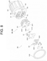
- the mounting member 2B includes a socket member 23 and a heat radiating member (heat sink member) 24.
- the socket member 23 is made of a material with thermal conductivity, a resin material in this example.
- the heat radiating member 24 is composed of a metal member or resin member with high thermal conductivity. Fin groove parts of the socket member 23 and heat radiation fin parts of the heat radiating member 24 are fitted and attached to each other via thermal conductive grease.
- the socket member 23 has a cylindrical portion 20 on one end side, a flange portion 21 on a central portion, fin portions 22 on the other end side, and a mounting projection (bayonet) 25 provided on the cylindrical portion 20.
- the flange portion 21 and the mounting projection 25 sandwich an edge of the mounting hole 103 of the lamp housing 102 together with the packing 105 to seal the inside of the lamp chamber 104 in a watertight state.
- the two terminals T4 and T5 are mounted on the socket member 23 in an insulated state.
- One end portions of the two terminals T4 and T5 and a portion of the socket member 23 form a connector unit 53 of the socket SB.
- the projecting surface part 240 and the recessed surface part 241 are provided on a front (front) installation surface of the heat radiating member 24.
- the projecting surface part 240 has a T shape when viewed from the front, and the recessed surface part 241 has a concave shape when viewed from the front like the shape of the circuit substrate 32 when viewed from the front.
- the back surface (rear surface) of the submount substrate 31 is mounted on a lower end of the projecting surface part 240 via the adhesive layer 242. Consequently, the semiconductor light-emitting element LED of the submount substrate 31 is disposed in a central portion of the installation surface of the heat radiating member 24.
- the back surface (rear surface) of the circuit substrate 32 is attached to the entire recessed surface part 241 via the adhesive layer 243. Consequently, the two terminals T4 and T5 and the two capacitors C 1 and C2 are disposed on a lower part of the installation surface of the heat radiating member 24.
- the other end portions of the two terminals T4 and T5 are inserted through the heat radiating member 24 and the circuit substrate 32 and crimped to the circuit substrate 32. Consequently, the circuit substrate 32 is securely attached to the heat radiating member 24.
- the connector 54 electrically connects the two terminals T4 and T5 to the control circuit 4 via the connector unit 53 of the socket SB.
- the connector 54 electrically connects the two terminals T4 and T5 to the control circuit 4 via the harnesses 61 and 62.
- the connector 54 has a power supply side terminal 541 and a ground side terminal 542.
- the power supply side terminal 541 is connected to the power supply side harness 61, and is detachably connected to the power supply terminal T4.
- the ground side terminal 542 is connected to the ground side harness 62, and is detachably connected to the ground terminal T5. Consequently, the connector 54 electrically connects the power supply terminal T4 and the ground terminal T5 to the control circuit 4.
- the light source unit 1B according to this third embodiment is configured as described above, and the action will be described in the following.
- the connector 54 is detachably attached to the connector unit 53 of the socket SB. Then, the power supply side terminal 541 of the connector 54 and the power supply terminal T4 of the connector unit 53 are electrically connected to each other, and the ground side terminal 542 of the connector 54 and the ground terminal T5 of the connector unit 53 are electrically connected to each other.
- control circuit 4 power supply side harness 61 ⁇ power supply side terminal 541 ⁇ power supply terminal T4 ⁇ semiconductor light-emitting element LED ⁇ ground terminal T5 ⁇ ground side terminal 542 ⁇ ground side harness 62 ⁇ control circuit 4. Consequently, a large number of light emitting chips of the semiconductor light-emitting element LED emit light.
- the semiconductor light-emitting element LED mounted on the submount substrate 31 has a plurality of the light emitting chips.
- the forward voltage of the one light emitting chip of the semiconductor light-emitting element LED is not higher than a predetermined operating voltage
- the forward voltage of a large number of the light emitting chips of the semiconductor light-emitting element LED becomes the predetermined operating voltage or more. Consequently, the control circuit 4 operates, and a large number of the light emitting chips of the semiconductor light-emitting element LED mounted on the submount substrate 31 emit light.
- a plurality of the light emitting chips of the semiconductor light-emitting element LED emit white light or amber light, or both white light and amber light.
- the light source unit 1B according to this third embodiment has the configuration and action as described above, and therefore it is possible to achieve the same effect as the light source unit 1 according to the above first embodiment.
- the semiconductor light-emitting element LED is mounted on the submount substrate 31 which is the one substrate, and the terminals T4 and T5 of the power supply member are mounted on the circuit substrate 32 which is the other substrate, and therefore the heat radiation effect is improved.
- the modification is an example in which the semiconductor light-emitting elements LED1 and LED2 are not mounted on the one substrate 3, but directly mounted on the mounting member (heat radiating member) 2, unlike the above first and second embodiments.
- the modification is an example in which the semiconductor light-emitting element LED is not mounted on the submount substrate 31 which is one of the divided two substrate, but directly mounted on the heat radiating member 24 of the mounting member 2B, unlike the above third embodiment.
- the semiconductor light-emitting elements LED1 and LED2 and the mounting member (heat radiating member) 2 need to be insulated via an insulating member, and the semiconductor light-emitting elements LED 1 and LED2 and the substrate 3 mounted on the mounting member (heat radiating member) 2 need to be electrically connected to each other.
- the semiconductor light-emitting element LED and the heat radiating member 24 of the mounting member 2B need to be insulated via an insulating member, and the semiconductor light-emitting element LED and the circuit substrate 32 which is the other of the divided two substrates mounted on the heat radiating member 24 of the mounting member 2B need to be electrically connected to each other.
- the semiconductor light-emitting elements LED 1 and LED2 are directly mounted on the mounting member (heat radiating member) 2, and the semiconductor light-emitting element LED is directly mounted on the heat radiating member 24 of the mounting member 2B, and therefore the heat radiation effect is improved.
- the light source units 1, 1A, 1B, and the vehicle lamps 100, 100A are used in combination with clearance lamps and daytime running lamps, or in combination with low beam lamps and high beam lamps.
- the light source unit for a vehicle lamp, and the vehicle lamp can be used for lamps in combinations other than the lamps in the above combination.
- control circuit 4 is disposed inside the lamp chamber 104.
- control circuit 4 may be disposed outside the lamp chamber 104.
- the one socket S, SB and the one control circuit 4 are electrically connected to each other via the connector 51 or 52, 54 and the harnesses 61 and 62.
- a plurality of the sockets S, SB and the one control circuit 4 may be electrically connected to via the connector 51 or 52, 54 and the harnesses 61 and 62.
- the present invention is not limited to the above first, second, and third embodiments, and the modification.
Landscapes
- Engineering & Computer Science (AREA)
- General Engineering & Computer Science (AREA)
- Physics & Mathematics (AREA)
- Microelectronics & Electronic Packaging (AREA)
- Optics & Photonics (AREA)
- Mechanical Engineering (AREA)
- Non-Portable Lighting Devices Or Systems Thereof (AREA)
- Lighting Device Outwards From Vehicle And Optical Signal (AREA)
Abstract
Description
- The present invention relates to a light source unit for a vehicle lamp, and a vehicle lamp.
- As a light source unit for a vehicle lamp and a vehicle lamp, in which a semiconductor light-emitting element and a control circuit are separately configured, there is, for example,
PTL 1. In the following,PTL 1 will be described. - In a light source module for a vehicle lamp and a vehicle lamp in PTL 1 (hereinafter referred to as a "light source module in
PTL 1"), a light-emitting element is provided on a first substrate, a drive circuit is provided on a second substrate, and the first substrate is mounted on a first housing, and the second substrate is mounted on a second housing. - The light source module in
PTL 1 divides the first substrate on the light-emitting element side and the second substrate on the drive circuit side, the light-emitting element is separated from heat of the drive circuit, and luminous efficiency of the light-emitting element is improved. - PTL 1:
Japanese Patent Application Laid-open No. 2018-67451 - However, although the light source module in
PTL 1 divides the first substrate on the light-emitting element side and the second substrate on the drive circuit side, the first substrate on the light-emitting element side and the second substrate on the drive circuit side are integrally incorporated in a socket. As a result, in the light source module inPTL 1, the light-emitting element is affected by the heat of the drive circuit, and therefore further improvement of the luminous efficiency of the light-emitting element may be hindered. - The problem to be solved by the present invention is to provide a light source unit for a vehicle lamp and a vehicle lamp capable of further improving the luminous efficiency of a semiconductor light-emitting element.
- A light source unit for a vehicle lamp of the present invention includes: a mounting member mounted on the vehicle lamp; a substrate mounted on the mounting member; a semiconductor light-emitting element electrically connected to the substrate; a power supply member mounted on the mounting member and the substrate and electrically connected to the semiconductor light-emitting element; a control circuit that controls light emission of the semiconductor light-emitting element; and a connector that electrically connects the power supply member to the control circuit, wherein the mounting member, the substrate, the semiconductor light-emitting element, and the power supply member are configured as a socket which is an integral structure, and the control circuit is configured separately from the socket.
- In the light source unit for a vehicle lamp of the present invention, a plurality of the semiconductor light-emitting elements and a plurality of the power supply members are preferably provided, and the plurality of semiconductor light-emitting elements are preferably mounted on the substrate.
- In the light source unit for a vehicle lamp of the present invention, the control circuit preferably has an operating voltage for operating in a case where a forward voltage of the semiconductor light-emitting elements is a predetermined value, and the operating voltage of the control circuit preferably exceeds the predetermined value in a case where a plurality of the light source units for a vehicle lamp are provided.
- In the light source unit for a vehicle lamp of the present invention, the substrate is preferably mounted with a resistor, a plurality of the power supply members are preferably composed of: a first terminal that supplies power to a plurality of the semiconductor light-emitting elements via the resistor; a second terminal that supplies power to a plurality of the semiconductor light-emitting elements without going through the resistor; and a common ground terminal, and the connector is preferably composed of a first connector that electrically connects the first terminal and the ground terminal to the control circuit, or a second connector that electrically connects the second terminal and the ground terminal to the control circuit.
- In the light source unit for a vehicle lamp of the present invention, the socket and the control circuit of the light source unit for a vehicle lamp are preferably a common socket and a common control circuit, in a case where a forward voltage of the semiconductor light-emitting element is less than a predetermined operating voltage of the control circuit, the first terminal and the ground terminal are preferably electrically connected to the control circuit by the first connector, and in a case where the forward voltage of the semiconductor light-emitting element is not less than the predetermined operating voltage of the control circuit, the second terminal and the ground terminal are preferably electrically connected to the control circuit by the second connector.
- In the light source unit for a vehicle lamp of the present invention, the control circuit preferably controls a low beam lamp unit and a high beam lamp unit.
- In the light source unit for a vehicle lamp of the present invention, a plurality of the semiconductor light-emitting elements are preferably mounted on a central portion of the substrate, a plurality of the power supply members are preferably mounted on a lower edge portion of the substrate, and the resistor is preferably provided on an upper edge portion of the substrate.
- In the light source unit for a vehicle lamp of the present invention, the semiconductor light-emitting element is preferably mounted on the mounting member.
- In the light source unit for a vehicle lamp of the present invention, the substrate preferably has: a first substrate mounted with the semiconductor light-emitting element; and a second substrate mounted with the power supply member, the first substrate and the second substrate are electrically connected to each other, the semiconductor light-emitting element and the power supply member are electrically connected to each other via the first substrate and the second substrate.
- A vehicle lamp of the present invention includes: a lamp housing and a lamp lens that form a lamp chamber; and the light source unit for a vehicle lamp of the present invention, wherein in the socket of the light source unit for a vehicle lamp, a portion on a semiconductor light-emitting element side is disposed inside the lamp chamber and a portion on a power supply member side is disposed outside the lamp chamber, or an entire portion is disposed inside the lamp chamber, and the control circuit of the light source unit for a vehicle lamp is disposed inside or outside the lamp chamber, separately from the socket, and is electrically connected to a battery.
- In a light source unit for a vehicle lamp and a vehicle lamp of the present invention, it is possible to further improve luminous efficiency of a semiconductor light-emitting element.
-
- [
FIG. 1] FIG. 1 is a schematic vertical cross-sectional view of a use state illustrating a first embodiment of a light source unit for a vehicle lamp and a vehicle lamp according to the present invention. - [
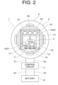
FIG. 2] FIG. 2 is a front view illustrating a socket (a view taken along an arrow II inFIG. 1 ). - [
FIG. 3] FIG. 3 is an electric circuit diagram illustrating a state in which a first terminal and a ground terminal are electrically connected via a first connector. - [
FIG. 4] FIG. 4 is an electric circuit diagram illustrating a state in which a second terminal and the ground terminal are electrically connected via a second connector. - [
FIG. 5] FIG. 5 is a schematic vertical cross-sectional view (a schematic vertical cross-sectional view corresponding toFIG. 1 ) of a use state illustrating a second embodiment of the light source unit for a vehicle lamp and a vehicle lamp according to the present invention. - [
FIG. 6] FIG. 6 is a front view (a front view corresponding toFIG. 2 ) of a socket illustrating a third embodiment of the light source unit for a vehicle lamp and a vehicle lamp according to the present invention. - [
FIG. 7] FIG. 7 is a perspective view illustrating the socket. - [
FIG. 8] FIG. 8 is an exploded perspective view illustrating the socket. - [
FIG. 9] FIG. 9 is an electric circuit diagram illustrating a state in which a power terminal and the ground terminal are electrically connected via a connector. - Hereinafter, three embodiments (practical examples) of a light source unit for a vehicle lamp and a vehicle lamp according to the present invention and a modification will be described in detail with reference to the drawings.
- In this specification, front, rear, top, bottom, left, and right refer to front, rear, top, bottom, left, and right when the light source unit for a vehicle lamp and the vehicle lamp according to the present invention is mounted on a vehicle (not illustrated).
- Since the drawings are schematic diagrams illustrating the light source unit for a vehicle lamp and the vehicle lamp according to the present invention, the details of the light source unit for a vehicle lamp and the vehicle lamp according to the present invention are omitted in the drawings. In addition, some hatching is omitted.
-
FIG. 1 to FIG. 4 each illustrate a first embodiment of the light source unit for a vehicle lamp and the vehicle lamp according to the present invention. Hereinafter, configurations of alight source unit 1 for a vehicle lamp according to this first embodiment (hereinafter, referred to as the "light source unit 1") and avehicle lamp 100 according to this first embodiment (hereinafter, referred to as the "vehicle lamp 100") will be described. - In this example, the
vehicle lamp 100 is a front combination lamp. Thevehicle lamp 100 is installed on each of the left and right sides of the front of the vehicle (not illustrated). As illustrated inFIG. 1 , thevehicle lamp 100 includes alamp housing 102, alamp lens 101, and thelight source unit 1. - The
lamp housing 102 is made of, for example, a light impermeable resin member. Thelamp housing 102 has a hollow shape with one side open and the other side closed. Amounting hole 103 is provided in a closing part of thelamp housing 102. - The
lamp lens 101 is made of, for example, a light transmissive resin member or a glass member. Thelamp lens 101 has a hollow shape with one side open and the other side closed. A periphery of an opening of thelamp lens 101 and a periphery of an opening of thelamp housing 102 are fixed in a watertight state. Alamp chamber 104 is formed by thelamp housing 102 and thelamp lens 101. - In this example, the
light source unit 1 is a light source unit that is used as both a daytime running lamp and a clearance lamp, or a light source unit that is used as both a high beam lamp and a low beam lamp. Herein, the light intensity (luminous flux, lumen: lm) of the daytime running lamp is greater than the light intensity of the clearance lamp. In addition, the light intensity of the high-beam lamp is greater than the light intensity of the low-beam lamp. - As illustrated in
FIG. 1 to FIG. 4 , thelight source unit 1 includes amounting member 2, asubstrate 3, a plurality of semiconductor light-emitting element LEDs, two semiconductor light-emitting elements LED1 and LED2 in this example, and a plurality of power supply members, three power supply members (three terminals T1, T2 and T3) in this example, acontrol circuit 4, and aconnector - The
mounting member 2, thesubstrate 3, the two semiconductor light-emitting elements LED1 and LED2, and the three power supply members T1, T2, and T3 are configured as a socket S that is an integrated structure. Thecontrol circuit 4 is configured separately from the socket S, for example, as an LDM (LED Driver Module). - As illustrated in
FIG. 1 andFIG. 2 , themounting member 2 constitutes a main body portion of the socket S. Themounting member 2 is detachably attached to an edge of themounting hole 103 of thelamp housing 102 via a packing (O-ring) 105. - Most of the mounting
member 2 is composed of a heat radiating member, and has acylindrical portion 20 on one end portion side, aflange portion 21 on the central portion side, andfin portions 22 on the other end portion side. Thecylindrical portion 20 is disposed inside thelamp chamber 104. Theflange portion 21 and thefin portions 22 are disposed outside thelamp chamber 104. Theflange portion 21 sandwiches the packing 105 together with the edge of the mountinghole 103 of thelamp housing 102 to seal the inside of thelamp chamber 104 in a watertight state. - As illustrated in
FIG. 2 ,FIG. 3 andFIG. 4 , in this example, thesubstrate 3 has a square plate shape when viewed from the front, and is composed of a ceramic substrate. Thesubstrate 3 is mounted inside the cylindrical portion of the mountingmember 2 directly or via a metal plate. - On a front surface of the
substrate 3, a plurality of semiconductor light-emitting elements, the two semiconductor light-emitting elements LED 1 and LED2 in this example, a plurality of three resistors, the three resistors R1, R2 and R3 in this example, a plurality of capacitors, the two capacitors C1 and C2 in this example are mounted. In addition, a wiring pattern is formed on the front surface of thesubstrate 3. - As illustrated in
FIG. 2 ,FIG. 3 andFIG. 4 , the two semiconductor light-emitting elements LED1 and LED2 are, for example, LED chips, and are mounted on a central portion of the front surface of thesubstrate 3. - As illustrated in
FIG. 2 ,FIG. 3 andFIG. 4 , one portions of the three power supply members T1, T2 and T3 are mounted on the mountingmember 2 and thesubstrate 3, and are electrically connected to the two semiconductor light-emitting elements LED1 and LED2 via the three resistors R1, R2 and R3, the two capacitors C1 and C2 and the wiring pattern. - The three power supply members T1, T2 and T3 are composed of a first terminal T1, a second terminal T2, and a third terminal T3. Hereinafter, the three power supply members T1, T2 and T3 are referred to as the three terminals T1, T2 and T3.
- The first terminal T1 supplies power to the two semiconductor light-emitting elements LED1 and LED2 via the three resistors R1, R2 and R3, as described below. The second terminal T2 supplies power to the two semiconductor light-emitting elements LED1 and LED2 directly without going through the three resistors R1, R2 and R3, as described below. The third terminal T3 is a common ground terminal.
- An insulating member is interposed between the three terminals T1, T2 and T3 and the mounting
member 2, and the three terminals T1, T2 and T3 and the mountingmember 2 are insulated from each other and integrated. The other end portions of the three terminals T1, T2 and T3 and a portion of thefin portions 22 of the mountingmember 2 form aconnector unit 50 of the socket S. Theconnector unit 50 is disposed outside thelamp chamber 104. - As illustrated in
FIG. 1 , thecontrol circuit 4 is electrically connected to thelight source unit 1 via theconnector unit 50 of the socket S, theconnector control circuit 4 supplies a constant current to thelight source unit 1. Thecontrol circuit 4 operates at a predetermined operating voltage (about 7 V in this example) or more and does not operate below the predetermined operating voltage. That is, thecontrol circuit 4 controls a daytime running lamp and a clearance lamp, as well as a high beam lamp and a low beam lamp, and therefore restriction of the above predetermined operating voltage occurs. - Herein, in the
light source unit 1, in a case where the forward voltage of one semiconductor light-emitting element is 3 V, the forward voltage of the two semiconductor light-emitting elements LED 1 and LED2 is 6 V. In this state, thecontrol circuit 4 does not operate, and the two semiconductor light-emitting elements LED1 and LED2 of thelight source unit 1 do not light up. Therefore, inlight source unit 1, it is necessary to connect the two semiconductor light-emitting elements LED1 and LED2 to the three resistors R1, R2 and R3 (seeFIG. 3 ). On the other hand, in a case where the two or morelight source units 1 are disposed in thevehicle lamp 100, the voltage is 6 V × 2 = 12 V or more, and therefore the two semiconductor light-emitting elements LED1 and LED2 do not need to be connected to the three resistors R1, R2 and R3 (seeFIG. 4 ). - As illustrated in
FIG. 1 , thecontrol circuit 4 is disposed inside thelamp chamber 104. Thecontrol circuit 4 disposed inside thelamp chamber 104 is electrically connected to a battery B via aharness 60. The battery B is disposed outside thelamp chamber 104. Theharness 60 is wired between the inside and the outside of thelamp chamber 104 via a grommet G attached to thelamp housing 102 in a watertight state. The battery B is a 12 V power supply. - As illustrated in
FIG. 1 ,FIG. 3 andFIG. 4 , theconnector control circuit 4 via theconnector unit 50 of the socket S. Theconnector connector unit 50 of the socket S form a waterproof structure. - The
connector connector unit 50 disposed outside thelamp chamber 104, and thecontrol circuit 4 disposed inside thelamp chamber 104 viaharnesses lamp chamber 104 via the grommet G attached to thelamp housing 102 in a watertight state, like theharness 60 described above. Theharnesses supply side harness 61 and aground side harness 62. - The
connector first connector 51 or asecond connector 52. - As illustrated in
FIG. 3 , thefirst connector 51 has a powersupply side terminal 511 and aground side terminal 512. The powersupply side terminal 511 is connected to the powersupply side harness 61, and is detachably connected to the first terminal T1. Theground side terminal 512 is connected to theground side harness 62, and is detachably connected to the ground terminal T3. Consequently, thefirst connector 51 electrically connects the first terminal T1 and the ground terminal T3 to thecontrol circuit 4. - As illustrated in
FIG. 4 , thesecond connector 52 has a powersupply side terminal 521 and aground side terminal 522. The powersupply side terminal 521 is connected to the powersupply side harness 61, and is detachably connected to the second terminal T2. Theground side terminal 522 is connected to theground side harness 62, and is detachably connected to the ground terminal T3. Consequently, thesecond connector 52 electrically connects the second terminal T2 and the ground terminal T3 to thecontrol circuit 4. - As illustrated in
FIG. 2 ,FIG. 3 andFIG. 4 , on thesubstrate 3, an electric circuit composed of the two semiconductor light-emitting elements LED 1 and LED2, the three terminals T1, T2 and T3, the three resistors R1, R2 and R3, the two capacitors C1 and C2, and the wiring pattern is formed. - The two semiconductor light-emitting elements LED1 and LED2 are disposed on the central portion of the front surface of the
substrate 3. The three terminals T1, T2 and T3 are mounted on a lower edge portion of thesubstrate 3. The three resistors R1, R2 and R3 are provided on an upper edge portion of thesubstrate 3. As a result, the three terminals T1, T2 and T3 and the three resistors R1, R2 and R3 are disposed on the top and the bottom with the two semiconductor light-emitting elements LED1 and LED2 therebetween on thesubstrate 3. - The three resistors R1, R2 and R3 are connected to the first terminal T1. The three resistors R1, R2 and R3 drop (reduce) a voltage between the first terminal T1 and the ground terminal T3 more than a voltage between the second terminal T2 and the ground terminal T3.
- The two capacitors C1 and C2 are provided below the central portion of the
substrate 3. The two capacitors C1 and C2 prevent the two semiconductor light-emitting elements LED1 and LED2 from erroneously emitting light due to noise from a power supply line. The power supply line includes theharnesses - The
light source unit 1 and thevehicle lamp 100 according to the this first embodiment are configured as described above, and the action thereof will be described in the following. - As illustrated in
FIG. 3 , thefirst connector 51 is detachably mounted on theconnector unit 50 of the socket S. Then, the powersupply side terminal 511 of thefirst connector 51 and the first terminal T1 of theconnector unit 50 are electrically connected to each other, and theground side terminal 512 of thefirst connector 51 and the ground terminal T3 of theconnector unit 50 are electrically connected to each other. - As a result, a current flows as follows: control
circuit 4 → powersupply side harness 61 → powersupply side terminal 511 → first terminal T1 → three resistors R1, R2 and R3 → two semiconductor light-emitting elements LED 1 and LED2 → ground terminal T3 →ground side terminal 512 →ground side harness 62 →control circuit 4. Consequently, the two semiconductor light-emitting elements LED1 and LED2 emit light. - As illustrated in
FIG. 4 , thesecond connector 52 is detachably mounted on theconnector unit 50 of the socket S. Then, the powersupply side terminal 521 of thesecond connector 52 and the second terminal T2 of theconnector unit 50 are electrically connected to each other, and theground side terminal 522 of thesecond connector 52 and the ground terminal T3 of theconnector unit 50 are electrically connected to each other. - As a result, a current flows as follows: control
circuit 4 → powersupply side harness 61 → powersupply side terminal 521 → second terminal T2 → two semiconductor light-emitting elements LED1 and LED2 → ground terminal T3 →ground side terminal 522 →ground side harness 62 →control circuit 4. Consequently, the two semiconductor light-emitting elements LED1 and LED2 emit light. - Herein, in a case where the forward voltage of the two semiconductor light-emitting elements LED1 and LED2 of the
light source unit 1 is less than the operating voltage of thecontrol circuit 4, for example, in a case where the onelight source unit 1 is disposed in thevehicle lamp 100, thefirst connector 51 is connected to theconnector unit 50 of the socket S as illustrated inFIG. 3 . A current is then supplied to the two semiconductor light-emitting elements LED1 and LED2 via the three resistors R1, R2 and R3. As a result, the forward voltage of the two semiconductor light-emitting elements LED1 and LED2 is not more than the predetermined operating voltage, but the voltage of the onelight source unit 1 is not lower than a predetermined operating voltage, and therefore thecontrol circuit 4 operates, and the two semiconductor light-emitting elements LED 1 and LED2 of the onelight source unit 1 emit light. - On the other hand, in a case where the forward voltage of the two semiconductor light-emitting elements LED1 and LED2 of the
light source unit 1 is not lower than the operating voltage of thecontrol circuit 4, for example, in a case where the twolight source units 1 are disposed in thevehicle lamp 100, thesecond connector 52 is connected to theconnector unit 50 of the socket S as illustrated inFIG. 4 . Then, a current is supplied directly to the two semiconductor light-emitting elements LED1 and LED2 without going through the three resistors R1, R2 and R3. As a result, even when the forward voltage of the two semiconductor light-emitting elements LED 1 and LED2 is not more than the predetermined operating voltage, the voltage of the twolight source units 1 is not less than the predetermined operating voltage, and therefore thecontrol circuit 4 operates, and the two semiconductor light-emitting elements LED1 and LED2 of the two or morelight source units 1 emit light respectively. - The
light source unit 1 and thevehicle lamp 100 according to this first embodiment have the above configuration and action, and their effects will be described in the following. - In the
light source unit 1 and thevehicle lamp 100 according to this first embodiment, while the mountingmember 2, thesubstrate 3, the two semiconductor light-emitting elements LED1 and LED2, and the three terminals T1, T2 and T3 are configured as the socket S which is an integrated structure, thecontrol circuit 4 is configured separately from the socket S. - As a result, the
light source unit 1 and thevehicle lamp 100 according to this first embodiment can shield the semiconductor light-emitting elements LED 1 and LED2 on the socket S side, which are separated from thecontrol circuit 4, from heat of thecontrol circuit 4. Consequently, thelight source unit 1 and thevehicle lamp 100 according to this first embodiment can increase a current value to be supplied to the semiconductor light-emitting elements LED1 and LED2, and the brightness of the lamp can be increased accordingly. For example, thelight source unit 1 and thevehicle lamp 100 according to this first embodiment can increase the light intensity of the semiconductor light-emitting elements LED1 and LED2 by about 20% or more compared to the light source module inPTL 1. Thus, in thelight source unit 1 and thevehicle lamp 100 according to this first embodiment, it is possible to further improve the luminous efficiency of the semiconductor light-emitting elements LED1 and LED2. - In the
light source unit 1 and thevehicle lamp 100 according to this first embodiment, since thecontrol circuit 4 is separated from thesubstrate 3 of the socket S, the socket S only needs to release the heat of the semiconductor light-emitting elements LED1 and LED2 to the outside, as the socket S, and therefore the socket S can be made smaller. That is, in the case of a socket that releases the heat of the semiconductor light-emitting element and the heat of the control circuit to the outside, the size increases. In particular, as the light intensity of the semiconductor light-emitting element increases, the heat of the semiconductor light-emitting element tends to rise and the size tends to increase. On the other hand, thelight source unit 1 and thevehicle lamp 100 according to this first embodiment each have the socket S that releases the heat of the semiconductor light-emitting elements LED 1 and LED2 to the outside, and therefore it is possible to reduce the size of the socket S. - In each of the
light source unit 1 and thevehicle lamp 100 according to this first embodiment, thecontrol circuit 4 is separated from thesubstrate 3 of the socket S, and therefore the area for mounting the parts and the area for forming the electric circuit on thesubstrate 3 can be expanded by separating thecontrol circuit 4. As a result, in each of thelight source unit 1 and thevehicle lamp 100 according to this first embodiment, is it possible to mount the terminals T1, T2 and T3 on thesubstrate 3 by adding the terminals T1, T2 and T3, and form thelight source unit 1 or thevehicle lamp 100 by adding an electric circuit. Consequently, with each of thelight source unit 1 and thevehicle lamp 100 according to this first embodiment, the onelight source unit 1 can be used in combination with two lamps with different lamp functions. - In the
light source unit 1 and thevehicle lamp 100 according to this first embodiment, thecontrol circuit 4 has an operating voltage for operating when the forward voltage of the semiconductor light-emitting elements LED 1 and LED2 is a predetermined value, and in a case where a plurality of thelight source units 1 are installed, the operating voltage of thecontrol circuit 4 exceeds the predetermined value. As a result, thelight source unit 1 and thevehicle lamp 100 according to this first embodiment can each use an existing control circuit as thecontrol circuit 4, and therefore a manufacturing cost can be reduced accordingly. - In each of the
light source unit 1 and thevehicle lamp 100 according to this first embodiment, the three terminals T1, T2 and T3 added and mounted on thesubstrate 3 are composed of the first terminal T1 that supplies power to the semiconductor light-emitting elements LED1 and LED2 via the resistors R1, R2 and R3, the second terminal T2 that directly supplies power to the semiconductor light-emitting elements LED1 and LED2 without going through the resistors R1, R2 and R3, and the common ground terminal T3. In addition, in each of thelight source unit 1 and thevehicle lamp 100 according to this first embodiment, theconnectors first connector 51 that connects the first terminal T1 and the ground terminal T3 to thecontrol circuit 4, or thesecond connector 52 that connects the second terminal T2 and the ground terminal T3 to thecontrol circuit 4. - As a result, as described above, in each of the
light source unit 1 and thevehicle lamp 100 according to this first embodiment, since thecontrol circuit 4 is separated from thesubstrate 3 of socket S, thesubstrate 3 can be shielded from the heat ofcontrol circuit 4, and therefore the current to be supplied to the semiconductor light-emitting elements LED1 and LED2 can be increased, and the brightness of the lamp can be increased accordingly. - In each of the
light source unit 1 and thevehicle lamp 100 according to this first embodiment, in a case where the forward voltage of the two semiconductor light-emitting elements LED1 and LED2 of thelight source unit 1 is less than the predetermined operating voltage of thecontrol circuit 4, for example, in a case where the onelight source unit 1 is disposed in thevehicle lamp 100, as illustrated inFIG. 3 , thefirst connector 51 is connected to theconnector unit 50 of the socket S. Then, a current is supplied to the two semiconductor light-emitting elements LED1 and LED2 via the three resistors R1, R2 and R3, and therefore in the forward voltage of the two semiconductor light-emitting elements LED1 and LED2 is not more than the predetermined operating voltage, but the voltage of the onelight source unit 1 is not less than the predetermined operating voltage, and therefore thecontrol circuit 4 operates, and the two semiconductor light-emitting elements LED 1 and the LED2 of the onelight source unit 1 emit light. - Further, in each of the
light source unit 1 and thevehicle lamp 100 according to this first embodiment, when the forward voltage of the two semiconductor light-emitting elements LED1 and LED2 of thelight source unit 1 is not lower than the predetermined operating voltage of thecontrol circuit 4, for example, when the two or morelight source units 1 are disposed in thevehicle lamp 100, as illustrated inFIG. 4 , thesecond connector 52 is connected to theconnector unit 50 of the socket S. Then, the current is directly supplied to the two semiconductor light-emitting elements LED1 and LED2 without going through the three resistors R1, R2 and R3, and therefore even when the forward voltage of the two semiconductor light-emitting elements LED1 and LED2 is not more than the predetermined operating voltage, the voltage of the twolight source units 1 is not less than predetermined operating voltage, and therefore thecontrol circuit 4 operates, and the two semiconductor light-emitting elements LED 1 and LED2 of the two or morelight source units 1 each emit light. - As a result, in each of the
light source unit 1 and thevehicle lamp 100 according to this first embodiment, the common socket S and thecontrol circuit 4 can be used as the socket S and thecontrol circuit 4, respectively. Consequently, in each of thelight source unit 1 and thevehicle lamp 100 according to this first embodiment, it is possible to reduce a manufacturing cost. - In each of the
light source unit 1 and thevehicle lamp 100 according to this first embodiment, thecontrol circuit 4 controls a low beam lamp unit and a high beam lamp unit. As a result, in each of thelight source unit 1 and thevehicle lamp 100 according to this first embodiment, thecontrol circuit 4 can also be used as a control circuit for the low beam lamp unit and the high beam lamp unit, and can be made common. Consequently, in each of thelight source unit 1 and thevehicle lamp 100 according to this first embodiment, it is possible to reduce a manufacturing cost. - In each of the
light source unit 1 and thevehicle lamp 100 according to this first embodiment, the semiconductor light-emitting elements LED 1 and LED2 are mounted on the central portion of thesubstrate 3, the terminals T1, T2 and T3 are mounted on the lower edge portion of thesubstrate 3, and the resistors R1, R2 and R3 are provided on the upper edge portion of thesubstrate 3. That is, in each of thelight source unit 1 and thevehicle lamp 100 according to this first embodiment, the three terminals T1, T2 and T3 and the three resistors R1, R2 and R3 are disposed on the top and the bottom with the two semiconductor light-emitting elements LED1 and LED2 therebetween. - As a result, in each of the
light source unit 1 and thevehicle lamp 100 according to this first embodiment, spaces between the semiconductor light-emitting elements LED1 and LED2, and the terminals T1, T2 and T3 and the resistors R1, R2 and R3 can be widened. Consequently, in each of thelight source unit 1 and thevehicle lamp 100 according to this first embodiment, a complex electric circuit can be formed between the semiconductor light-emitting elements LED1 and LED2, and the terminals T1, T2 and T3 and the resistors R1, R2 and R3. - In each of the
light source unit 1 and thevehicle lamp 100 according to this first embodiment, the semiconductor light-emitting elements LED 1 and LED2 are mounted on the central portion of thesubstrate 3, and therefore light from the semiconductor light-emitting elements LED1 and LED2 can be controlled easily and accurately, compared to a case where the semiconductor light-emitting elements LED1 and LED2 are mounted on an edge of thesubstrate 3. The semiconductor light-emitting elements LED 1 and LED2 emit white light or amber light, or white light and amber light. - In each of the
light source unit 1 and thevehicle lamp 100 according to this first embodiment, the resistors R1, R2 and R3 are provided in the upper edge portion of thesubstrate 3, that is, a portion above the semiconductor light-emitting elements LED1 and LED2, and therefore due to the action of an updraft, the semiconductor light-emitting elements LED1 and LED2 can be shielded from the heat of the resistors R1, R2 and R3, and the luminous efficiency of the semiconductor light-emitting elements LED 1 and LED2 can be improved. - In the
vehicle lamp 100 according to this first embodiment, theflange portion 21 and thefin portions 22 of the socket S of thelight source unit 1 are disposed outside thelamp chamber 104, and therefore the heat radiation effect of thelight source unit 1 is improved. - In the
vehicle lamp 100 according to this first embodiment, thecontrol circuit 4 is disposed inside thelamp chamber 104, and therefore thecontrol circuit 4 can be protected from the environment outside thelamp chamber 104, and the performance of thecontrol circuit 4 is improved. -
FIG. 5 illustrates a second embodiment of the light source unit for a vehicle lamp and the vehicle lamp according to the present invention. Hereinafter, a configuration, action and an effect of alight source unit 1A for a vehicle lamp and avehicle lamp 100A according to this second embodiment will be described. In the drawing, the same reference numerals as those inFIG. 1 to FIG. 4 denote the same components. - In each of the
light source unit 1 for a vehicle lamp and thevehicle lamp 100 according to the above first embodiment, thecylindrical portion 20 on the semiconductor light-emitting elements LED 1 and LED2 side of the socket S is disposed inside thelamp chamber 104, and theflange portion 21 and thefin portions 22 on the terminals T1, T2 and T3 side of the socket S are disposed outside thelamp chamber 104. On the other hand, in each of thelight source unit 1A for a vehicle lamp and thevehicle lamp 100A according to this second embodiment, the entire socket S is disposed inside thelamp chamber 104. - The
light source unit 1A for a vehicle lamp and thevehicle lamp 100A according to this second embodiment are configured as described above, and therefore it is possible to achieve the same action effect as thelight source unit 1 for a vehicle lamp and thevehicle lamp 100 according to the above first embodiment. - In particular, in the
vehicle lamp 100A according to this second embodiment, the entire socket S of thelight source unit 1A is disposed inside thelamp chamber 104, and therefore thelight source unit 1A can be protected from the environment outside thelamp chamber 104, and performance of thelight source unit 1A is improved. -
FIG. 6 to FIG. 9 each illustrate a third embodiment of the light source unit for a vehicle lamp according to the present invention. Hereinafter, a configuration of alight source unit 1B for a vehicle lamp according to this third embodiment will be described. In the drawing, the same reference numerals as those inFIG. 1 to FIG. 5 denote the same components. - As illustrated in
FIG. 6 to FIG. 9 , thelight source unit 1B for a vehicle lamp according to this third embodiment includes a mountingmember 2B, twosubstrates control circuit 4, and aconnector 54, almost similar to thelight source units - The mounting
member 2B, the twosubstrates control circuit 4 is configured separately from the socket SB, for example, as an LDM (LED Driver Module). - In each of the
light source units substrate 3, and the terminals T1, T2 and T3 of the power supply member are mounted, the semiconductor light-emitting elements LED1 and LED2, the terminals T1, T2 and T3 are electrically connected to each other via the onesubstrate 3. - On the other hand, in the
light source unit 1B for a vehicle lamp according to this third embodiment, the substrate is divided into two substrates, namely, asubmount substrate 31 as a first substrate mounted with the semiconductor light-emitting element LED, and acircuit substrate 32 as a second substrate mounted with the two terminals T4 and T5 of the power supply member, and the semiconductor light-emitting element LED and the terminals T4 and T5 are electrically connected to each other via the twosubstrate - As illustrated in
FIG. 8 , one substrate is divided into two, one of the substrates is defined as thesubmount substrate 31 as the first substrate, and the other is defined as thecircuit substrate 32 as the second substrate. The front view of thesubmount substrate 31 has a horizontally long small rectangular shape, and the front view of thecircuit substrate 32 has a concave shape. - The semiconductor light-emitting element (light emitting chip) LED is attached to (mounted on) the upper half of a front (front) mounting surface of the
submount substrate 31. Twoconnection terminals 310 are provided at the two lower corners of the mounting surface of thesubmount substrate 31. The semiconductor light-emitting element LED and the twoconnection terminals 310 are electrically connected to each other via wires on thesubmount substrate 31. Consequently, the semiconductor light-emitting element LED is mounted and electrically connected to thesubmount substrate 31 as the first substrate. A back surface (rear surface) of thesubmount substrate 31 is mounted on a projectingsurface part 240, described below, of the mountingmember 2B via anadhesive layer 242. - The two terminals T4 and T5, two
connection terminals 320 and two capacitors C1 and C2 are attached to (mounted on) thecircuit substrate 32. The two terminals T4 and T5, the twoconnection terminals 320 and the two capacitors C1 and C2 are electrically connected to each other via wires on thecircuit substrate 32. - Consequently, the two capacitors C1 and C2 are mounted and electrically connected to a bottom center of the
circuit substrate 32 as the second substrate. The two terminals T4 and T5 are mounted and electrically connected to the left and right sides of the two capacitors C1 and C2 under thecircuit substrate 32 as the second substrate. The back surface (rear surface) of thecircuit substrate 32 is mounted on a recessedsurface part 241, described below, of the mountingmember 2B via anadhesive layer 243. - The two
connection terminals 310 of thesubmount substrate 31 and the twoconnection terminals 320 of thecircuit substrate 32 are electrically connected to each other by bondingwires 33. Consequently, the semiconductor light-emitting element LED and the terminals T4 and T5 are electrically connected to each other via thesubmount substrate 31 and thecircuit substrate 32. - As illustrated in
FIG. 8 , the mountingmember 2B includes asocket member 23 and a heat radiating member (heat sink member) 24. Thesocket member 23 is made of a material with thermal conductivity, a resin material in this example. Theheat radiating member 24 is composed of a metal member or resin member with high thermal conductivity. Fin groove parts of thesocket member 23 and heat radiation fin parts of theheat radiating member 24 are fitted and attached to each other via thermal conductive grease. - The
socket member 23 has acylindrical portion 20 on one end side, aflange portion 21 on a central portion,fin portions 22 on the other end side, and a mounting projection (bayonet) 25 provided on thecylindrical portion 20. Theflange portion 21 and the mountingprojection 25 sandwich an edge of the mountinghole 103 of thelamp housing 102 together with the packing 105 to seal the inside of thelamp chamber 104 in a watertight state. - The two terminals T4 and T5 are mounted on the
socket member 23 in an insulated state. One end portions of the two terminals T4 and T5 and a portion of thesocket member 23 form aconnector unit 53 of the socket SB. - The projecting
surface part 240 and the recessedsurface part 241 are provided on a front (front) installation surface of theheat radiating member 24. The projectingsurface part 240 has a T shape when viewed from the front, and the recessedsurface part 241 has a concave shape when viewed from the front like the shape of thecircuit substrate 32 when viewed from the front. - The back surface (rear surface) of the
submount substrate 31 is mounted on a lower end of the projectingsurface part 240 via theadhesive layer 242. Consequently, the semiconductor light-emitting element LED of thesubmount substrate 31 is disposed in a central portion of the installation surface of theheat radiating member 24. The back surface (rear surface) of thecircuit substrate 32 is attached to the entire recessedsurface part 241 via theadhesive layer 243. Consequently, the two terminals T4 and T5 and the twocapacitors C 1 and C2 are disposed on a lower part of the installation surface of theheat radiating member 24. - The other end portions of the two terminals T4 and T5 are inserted through the
heat radiating member 24 and thecircuit substrate 32 and crimped to thecircuit substrate 32. Consequently, thecircuit substrate 32 is securely attached to theheat radiating member 24. - As illustrated in
FIG. 9 , theconnector 54 electrically connects the two terminals T4 and T5 to thecontrol circuit 4 via theconnector unit 53 of the socket SB. In addition, theconnector 54 electrically connects the two terminals T4 and T5 to thecontrol circuit 4 via theharnesses - The
connector 54 has a powersupply side terminal 541 and aground side terminal 542. The powersupply side terminal 541 is connected to the powersupply side harness 61, and is detachably connected to the power supply terminal T4. Theground side terminal 542 is connected to theground side harness 62, and is detachably connected to the ground terminal T5. Consequently, theconnector 54 electrically connects the power supply terminal T4 and the ground terminal T5 to thecontrol circuit 4. - The
light source unit 1B according to this third embodiment is configured as described above, and the action will be described in the following. - As illustrated in
FIG. 9 , theconnector 54 is detachably attached to theconnector unit 53 of the socket SB. Then, the powersupply side terminal 541 of theconnector 54 and the power supply terminal T4 of theconnector unit 53 are electrically connected to each other, and theground side terminal 542 of theconnector 54 and the ground terminal T5 of theconnector unit 53 are electrically connected to each other. - As a result, a current flows as follows: control
circuit 4 → powersupply side harness 61 → powersupply side terminal 541 → power supply terminal T4 → semiconductor light-emitting element LED → ground terminal T5 →ground side terminal 542 →ground side harness 62 →control circuit 4. Consequently, a large number of light emitting chips of the semiconductor light-emitting element LED emit light. - In this third embodiment, the semiconductor light-emitting element LED mounted on the
submount substrate 31 has a plurality of the light emitting chips. As a result, even when the forward voltage of the one light emitting chip of the semiconductor light-emitting element LED is not higher than a predetermined operating voltage, when a current is directly supplied to a large number of the light emitting chips of the semiconductor light-emitting element LED without going through a resistor, the forward voltage of a large number of the light emitting chips of the semiconductor light-emitting element LED becomes the predetermined operating voltage or more. Consequently, thecontrol circuit 4 operates, and a large number of the light emitting chips of the semiconductor light-emitting element LED mounted on thesubmount substrate 31 emit light. At this time, a plurality of the light emitting chips of the semiconductor light-emitting element LED emit white light or amber light, or both white light and amber light. - The
light source unit 1B according to this third embodiment has the configuration and action as described above, and therefore it is possible to achieve the same effect as thelight source unit 1 according to the above first embodiment. - In particular, in the
light source unit 1B according to this third embodiment, one substrate divided into two, the semiconductor light-emitting element LED is mounted on thesubmount substrate 31 which is the one substrate, and the terminals T4 and T5 of the power supply member are mounted on thecircuit substrate 32 which is the other substrate, and therefore the heat radiation effect is improved. - In the above first and second embodiments, an example, in which the semiconductor light-emitting elements LED1 and LED2 are mounted on the one
substrate 3 and electrically connected to the onesubstrate 3, is described. In the above third embodiment, an example, in which the semiconductor light-emitting element LED is mounted on thesubmount substrate 31 which is one of the divided two substrates, and is electrically connected to thesubmount substrate 31, is described. Hereinafter, a modification which is an example different from the above first to third embodiments will be described. - The modification is an example in which the semiconductor light-emitting elements LED1 and LED2 are not mounted on the one
substrate 3, but directly mounted on the mounting member (heat radiating member) 2, unlike the above first and second embodiments. In addition, the modification is an example in which the semiconductor light-emitting element LED is not mounted on thesubmount substrate 31 which is one of the divided two substrate, but directly mounted on theheat radiating member 24 of the mountingmember 2B, unlike the above third embodiment. - In this modification, with respect to the first and second embodiments, the semiconductor light-emitting elements LED1 and LED2 and the mounting member (heat radiating member) 2 need to be insulated via an insulating member, and the semiconductor light-emitting elements LED 1 and LED2 and the
substrate 3 mounted on the mounting member (heat radiating member) 2 need to be electrically connected to each other. In this modification, with respect to the above third embodiment, the semiconductor light-emitting element LED and theheat radiating member 24 of the mountingmember 2B need to be insulated via an insulating member, and the semiconductor light-emitting element LED and thecircuit substrate 32 which is the other of the divided two substrates mounted on theheat radiating member 24 of the mountingmember 2B need to be electrically connected to each other. - In this modification, the semiconductor light-emitting elements LED 1 and LED2 are directly mounted on the mounting member (heat radiating member) 2, and the semiconductor light-emitting element LED is directly mounted on the
heat radiating member 24 of the mountingmember 2B, and therefore the heat radiation effect is improved. - In the above first, second, and third embodiments, the
light source units vehicle lamps - In the above first, second, and third embodiments, the
control circuit 4 is disposed inside thelamp chamber 104. However, in the present invention, thecontrol circuit 4 may be disposed outside thelamp chamber 104. - Furthermore, in the above first, second, and third embodiments, the one socket S, SB and the one
control circuit 4 are electrically connected to each other via theconnector harnesses control circuit 4 may be electrically connected to via theconnector harnesses - The present invention is not limited to the above first, second, and third embodiments, and the modification.
-
- 1, 1A, 1B light source unit (light source unit for a vehicle lamp)
- 2, 2B mounting member
- 20 cylindrical portion
- 21 flange portion
- 22 fin portion
- 23 socket member
- 24 heat radiating member (heat sink member)
- 240 projecting surface part
- 241 recessed surface part
- 242, 243 adhesive layer
- 25 mounting projection (bayonet)
- 3 substrate
- 31 submount substrate (first substrate, one of divided two substrates)
- 32 circuit substrate (second substrate, the other of divided two substrates)
- 4 control circuit (LDM)
- 50 connector unit
- 51 first connector
- 511 power supply side terminal
- 512 ground side terminal
- 52 second connector
- 521 power supply side terminal
- 522 ground side terminal
- 53 connector unit
- 54 connector
- 541 power supply side terminal
- 542 ground side terminal
- 60 harness
- 61 power supply side harness
- 62 ground side harness
- 100, 100A vehicle lamp
- 101 lamp lens
- 102 lamp housing
- 103 mounting hole
- 104 lamp chamber
- 105 packing
- B battery
- C1, C2 capacitor
- G grommet
- LED1, LED2 semiconductor light-emitting element
- LED semiconductor light-emitting element (light emitting chip)
- R1, R2, R3 resistor
- S, SB socket
- T1 first terminal (power supply member)
- T2 second terminal (power supply member)
- T3 ground terminal (power supply member)
- T4 power supply terminal (power supply member)
- T5 ground terminal (power supply member)
Claims (10)
- A light source unit for a vehicle lamp comprising:a mounting member (2, 2B) mounted on the vehicle lamp;a substrate (3) mounted on the mounting member (2, 2B);a semiconductor light-emitting element (LED1, LED2) electrically connected to the substrate (3);a power supply member (T1, T2, T3) mounted on the mounting member (2, 2B) and the substrate (3) and electrically connected to the semiconductor light-emitting element (LED1, LED2);a control circuit (4) that controls light emission of the semiconductor light-emitting element (LED1, LED2); anda connector (54) that electrically connects the power supply member (T1, T2, T3) to the control circuit (4), whereinthe mounting member (2, 2B), the substrate (3), the semiconductor light-emitting element (LED1, LED2), and the power supply member (T1, T2, T3) are configured as a socket which is an integral structure, andthe control circuit (4) is configured separately from the socket.
- The light source unit for a vehicle lamp according to claim 1, whereina plurality of the semiconductor light-emitting elements (LED 1, LED2) and a plurality of the power supply members (T1, T2, T3) are provided, andthe plurality of semiconductor light-emitting elements (LED1, LED2) are mounted on the substrate (3).
- The light source unit for a vehicle lamp according to claim 2, whereinthe control circuit (4) has an operating voltage for operating in a case where a forward voltage of the semiconductor light-emitting elements (LED1, LED2) is a predetermined value, andthe operating voltage of the control circuit (4) exceeds the predetermined value in a case where a plurality of the light source units for a vehicle lamp are provided.
- The light source unit for a vehicle lamp according to claim 2, whereinthe substrate (3) is mounted with a resistor (R1, R2, R3),the plurality of power supply members (T1, T2, T3) are composed of:a first terminal that supplies power to the plurality of semiconductor light-emitting elements (LED1, LED2) via the resistor (R1, R2, R3);a second terminal that supplies power to the plurality of semiconductor light-emitting elements (LED1, LED2) without going through the resistor (R1, R2, R3); anda common ground terminal, andthe connector (54) is composed of a first connector that electrically connects the first terminal and the ground terminal to the control circuit (4), or a second connector that electrically connects the second terminal and the ground terminal to the control circuit (4).
- The light source unit for a vehicle lamp according to claim 4, whereinthe socket and the control circuit (4) of the light source unit for a vehicle lamp are a common socket and a common control circuit (4),in a case where a forward voltage of the semiconductor light-emitting element (LED1, LED2) is less than a predetermined operating voltage of the control circuit (4), the first terminal and the ground terminal are electrically connected to the control circuit (4) by the first connector, andin a case where the forward voltage of the semiconductor light-emitting element (LED1, LED2) is not less than the predetermined operating voltage of the control circuit (4), the second terminal and the ground terminal are electrically connected to the control circuit (4) by the second connector.
- The light source unit for a vehicle lamp according to claim 5, wherein
the control circuit (4) controls a low beam lamp unit and a high beam lamp unit. - The light source unit for a vehicle lamp according to claim 4, whereinthe plurality of semiconductor light-emitting elements (LED1, LED2) are mounted on a central portion of the substrate (3),the plurality of power supply members (T1, T2, T3) are mounted on a lower edge portion of the substrate (3), andthe resistor (R1, R2, R3) is provided on an upper edge portion of the substrate (3).
- The light source unit for a vehicle lamp according to claim 1, wherein
the semiconductor light-emitting element (LED1, LED2) is mounted on the mounting member (2, 2B). - The light source unit for a vehicle lamp according to claim 1, whereinthe substrate (3) has:a first substrate mounted with the semiconductor light-emitting element (LED1, LED2); anda second substrate mounted with the power supply member (T1, T2, T3),the first substrate and the second substrate are electrically connected to each other,the semiconductor light-emitting element (LED 1, LED2) and the power supply member (T1, T2, T3) are electrically connected to each other via the first substrate and the second substrate.
- A vehicle lamp comprising:a lamp housing (102) and a lamp lens (101) that form a lamp chamber; andthe light source unit (1, 1A, 1B) for a vehicle lamp according to any one of claims 1 to 9, whereinin the socket of the light source unit for a vehicle lamp, a portion on a semiconductor light-emitting element side is disposed inside the lamp chamber and a portion on a power supply member side is disposed outside the lamp chamber, or an entire portion is disposed inside the lamp chamber, andthe control circuit of the light source unit for a vehicle lamp is disposed inside or outside the lamp chamber, separately from the socket, and is electrically connected to a battery.
Applications Claiming Priority (3)
| Application Number | Priority Date | Filing Date | Title |
|---|---|---|---|
| JP2020113111 | 2020-06-30 | ||
| JP2021048801A JP7491251B2 (en) | 2020-06-30 | 2021-03-23 | Light source unit for vehicle lighting fixture, vehicle lighting fixture |
| PCT/JP2021/023496 WO2022004472A1 (en) | 2020-06-30 | 2021-06-22 | Light source unit for vehicle lamp, vehicle lamp |
Publications (3)
| Publication Number | Publication Date |
|---|---|
| EP4174370A1 true EP4174370A1 (en) | 2023-05-03 |
| EP4174370A4 EP4174370A4 (en) | 2024-01-24 |
| EP4174370B1 EP4174370B1 (en) | 2025-10-29 |
Family
ID=79316239
Family Applications (1)
| Application Number | Title | Priority Date | Filing Date |
|---|---|---|---|
| EP21834182.4A Active EP4174370B1 (en) | 2020-06-30 | 2021-06-22 | Light source unit for vehicle lamp, vehicle lamp |
Country Status (4)
| Country | Link |
|---|---|
| US (1) | US12305822B2 (en) |
| EP (1) | EP4174370B1 (en) |
| CN (1) | CN115735079A (en) |
| WO (1) | WO2022004472A1 (en) |
Families Citing this family (1)
| Publication number | Priority date | Publication date | Assignee | Title |
|---|---|---|---|---|
| KR102778025B1 (en) * | 2022-05-06 | 2025-03-11 | 주식회사 비에스테크닉스 | LED lamp for vehicle applying MID and magnetic induction technology And Manufacturing method of the same |
Family Cites Families (24)
| Publication number | Priority date | Publication date | Assignee | Title |
|---|---|---|---|---|
| JP2008243476A (en) * | 2007-03-26 | 2008-10-09 | Koito Mfg Co Ltd | Vehicle lighting |
| US20100176751A1 (en) * | 2008-05-20 | 2010-07-15 | Panasonic Corporation | Semiconductor light-emitting device as well as light source device and lighting system including the same |
| JP2011146483A (en) | 2010-01-13 | 2011-07-28 | Ichikoh Ind Ltd | Light source unit of semiconductor type light source of lighting fixture for vehicle, and lighting fixture for vehicle |
| JP5407026B2 (en) * | 2010-06-03 | 2014-02-05 | 市光工業株式会社 | Light source unit of semiconductor light source for vehicle lamp, vehicle lamp |
| JP2012084280A (en) * | 2010-10-07 | 2012-04-26 | Ichikoh Ind Ltd | Light source unit of semiconductor type light source of vehicle lighting fixture, and vehicle lighting fixture |
| JP2015041452A (en) | 2013-08-21 | 2015-03-02 | スタンレー電気株式会社 | LED module and cooling structure for vehicle lamp provided with the same |
| JP6146613B2 (en) * | 2013-09-04 | 2017-06-14 | 東芝ライテック株式会社 | Automotive lighting device and automotive lamp |
| JP6238159B2 (en) * | 2013-09-10 | 2017-11-29 | パナソニックIpマネジメント株式会社 | Lighting device, headlight device using the same, and vehicle |
| JP6195119B2 (en) * | 2014-09-03 | 2017-09-13 | 東芝ライテック株式会社 | MOVING BODY LIGHTING DEVICE AND VEHICLE LIGHT |
| JP6331223B2 (en) * | 2014-09-24 | 2018-05-30 | 東芝ライテック株式会社 | Lighting device and lighting device |
| US10337717B2 (en) * | 2015-03-31 | 2019-07-02 | Koito Manufacturing Co., Ltd. | Light source unit, method of manufacturing the same, and vehicle lamp |
| JP2017021988A (en) * | 2015-07-10 | 2017-01-26 | 東芝ライテック株式会社 | LIGHT EMITTING DEVICE FOR VEHICLE, LIGHTING DEVICE FOR VEHICLE, AND VEHICLE LIGHT |
| US9909752B2 (en) | 2015-07-22 | 2018-03-06 | Putco, Inc. | LED lamp with a flexible heat sink |
| CN106560652B (en) * | 2015-10-02 | 2020-09-04 | 东芝照明技术株式会社 | Vehicle lamps |
| JP2017098089A (en) * | 2015-11-25 | 2017-06-01 | 東芝ライテック株式会社 | Vehicle lighting device |
| EP3200562A1 (en) * | 2016-02-01 | 2017-08-02 | Toshiba Lighting & Technology Corporation | Vehicle lighting device and vehicle lamp |
| JP6220005B2 (en) * | 2016-04-13 | 2017-10-25 | 株式会社小糸製作所 | Lamp unit |
| JP6713904B2 (en) | 2016-10-19 | 2020-06-24 | スタンレー電気株式会社 | Light source module for vehicle lamp and vehicle lamp |
| DE102018202464A1 (en) | 2018-02-19 | 2019-08-22 | Osram Gmbh | LIGHT MODULE, ARRANGEMENT, SET, PROCEDURE, HEADLAMP AND VEHICLE |
| JP7091839B2 (en) | 2018-05-29 | 2022-06-28 | 東芝ライテック株式会社 | Vehicle lighting equipment and vehicle lighting equipment |
| US10605427B1 (en) | 2018-10-24 | 2020-03-31 | Xuan Fan Electro-Optical Technology Co., Ltd. | Light source module and illumination device comprising the same |
| JP7161949B2 (en) * | 2019-01-24 | 2022-10-27 | 株式会社小糸製作所 | vehicle lamp |
| JP2020187837A (en) * | 2019-05-10 | 2020-11-19 | 東芝ライテック株式会社 | Vehicular lighting device and vehicular lighting fixture |
| CN215294804U (en) * | 2020-10-27 | 2021-12-24 | 东芝照明技术株式会社 | Vehicle lighting device and vehicle lamp |
-
2021
- 2021-06-22 US US18/003,862 patent/US12305822B2/en active Active
- 2021-06-22 CN CN202180046781.6A patent/CN115735079A/en active Pending
- 2021-06-22 WO PCT/JP2021/023496 patent/WO2022004472A1/en not_active Ceased
- 2021-06-22 EP EP21834182.4A patent/EP4174370B1/en active Active
Also Published As
| Publication number | Publication date |
|---|---|
| EP4174370B1 (en) | 2025-10-29 |
| CN115735079A (en) | 2023-03-03 |
| WO2022004472A1 (en) | 2022-01-06 |
| US20230258308A1 (en) | 2023-08-17 |
| EP4174370A4 (en) | 2024-01-24 |
| US12305822B2 (en) | 2025-05-20 |
Similar Documents
| Publication | Publication Date | Title |
|---|---|---|
| JP5779329B2 (en) | Vehicle lighting | |
| EP2434206A2 (en) | Light source unit of semiconductor-type light source of vehicle lighting device and vehicle lighting device | |
| JP5621489B2 (en) | Light source unit of semiconductor light source for vehicle lamp, vehicle lamp | |
| KR20120006448A (en) | Light source unit of semiconductor light source of vehicle luminaire, vehicle luminaire | |
| JP2011171277A (en) | Light source unit for semiconductor type light source of vehicle lighting device, and vehicle lighting device | |
| US10041645B2 (en) | Light source unit, lighting device, and vehicle | |
| JP5853689B2 (en) | Semiconductor type light source for vehicle lamp, semiconductor type light source unit for vehicle lamp, vehicle lamp | |
| US12305822B2 (en) | Light source unit for vehicle lamp, vehicle lamp | |
| JP2011146483A (en) | Light source unit of semiconductor type light source of lighting fixture for vehicle, and lighting fixture for vehicle | |
| JP2013077463A (en) | Semiconductor type light source for vehicular lamp fitting, semiconductor type light source unit for the same, and vehicular lamp fitting | |
| JP2012084280A (en) | Light source unit of semiconductor type light source of vehicle lighting fixture, and vehicle lighting fixture | |
| CN209341132U (en) | Vehicular illumination device and lamps apparatus for vehicle | |
| JP2019175773A (en) | Light source unit for vehicular lighting fixture, and vehicular lighting fixture | |
| US8829794B2 (en) | Vehicle lamp | |
| JP5407026B2 (en) | Light source unit of semiconductor light source for vehicle lamp, vehicle lamp | |
| JP7491251B2 (en) | Light source unit for vehicle lighting fixture, vehicle lighting fixture | |
| CN104061463A (en) | Lamp Device And Luminaire | |
| WO2013108666A1 (en) | Light fixture for vehicle | |
| JP6825920B2 (en) | Light source unit and vehicle lighting equipment | |
| JP5412618B2 (en) | Light source unit of semiconductor light source for vehicle lamp, vehicle lamp | |
| JP3116836U (en) | Light emitting diode module and vehicle lamp provided with the light emitting diode module | |
| JP2012084279A (en) | Light source unit of semiconductor type light source of vehicle lighting fixture, and vehicle lighting fixture | |
| JP2021158231A (en) | Light source module and lighting device | |
| JP2013239238A (en) | Vehicle lighting fixture | |
| KR20150108797A (en) | LED lighting apparatus |
Legal Events
| Date | Code | Title | Description |
|---|---|---|---|
| STAA | Information on the status of an ep patent application or granted ep patent |
Free format text: STATUS: THE INTERNATIONAL PUBLICATION HAS BEEN MADE |
|
| PUAI | Public reference made under article 153(3) epc to a published international application that has entered the european phase |
Free format text: ORIGINAL CODE: 0009012 |
|
| STAA | Information on the status of an ep patent application or granted ep patent |
Free format text: STATUS: REQUEST FOR EXAMINATION WAS MADE |
|
| 17P | Request for examination filed |
Effective date: 20221230 |
|
| AK | Designated contracting states |
Kind code of ref document: A1 Designated state(s): AL AT BE BG CH CY CZ DE DK EE ES FI FR GB GR HR HU IE IS IT LI LT LU LV MC MK MT NL NO PL PT RO RS SE SI SK SM TR |
|
| DAV | Request for validation of the european patent (deleted) | ||
| DAX | Request for extension of the european patent (deleted) | ||
| A4 | Supplementary search report drawn up and despatched |
Effective date: 20240103 |
|
| RIC1 | Information provided on ipc code assigned before grant |
Ipc: B60Q 1/00 20060101ALN20231220BHEP Ipc: F21W 103/55 20180101ALI20231220BHEP Ipc: F21W 103/10 20180101ALI20231220BHEP Ipc: F21W 102/13 20180101ALI20231220BHEP Ipc: F21S 45/48 20180101ALI20231220BHEP Ipc: F21S 45/00 20180101ALI20231220BHEP Ipc: F21S 43/19 20180101ALI20231220BHEP Ipc: F21S 43/14 20180101ALI20231220BHEP Ipc: F21S 41/19 20180101ALI20231220BHEP Ipc: F21S 41/143 20180101ALI20231220BHEP Ipc: F21W 105/00 20180101ALI20231220BHEP Ipc: F21Y 115/10 20160101ALI20231220BHEP Ipc: F21V 29/77 20150101ALI20231220BHEP Ipc: F21V 29/503 20150101ALI20231220BHEP Ipc: F21V 23/06 20060101ALI20231220BHEP Ipc: F21V 23/00 20150101ALI20231220BHEP Ipc: B60Q 1/28 20060101ALI20231220BHEP Ipc: B60Q 1/04 20060101ALI20231220BHEP Ipc: F21K 9/23 20160101ALI20231220BHEP Ipc: F21V 19/00 20060101ALI20231220BHEP Ipc: F21V 31/00 20060101AFI20231220BHEP |
|
| STAA | Information on the status of an ep patent application or granted ep patent |
Free format text: STATUS: EXAMINATION IS IN PROGRESS |
|
| 17Q | First examination report despatched |
Effective date: 20241011 |
|
| GRAP | Despatch of communication of intention to grant a patent |
Free format text: ORIGINAL CODE: EPIDOSNIGR1 |
|
| STAA | Information on the status of an ep patent application or granted ep patent |
Free format text: STATUS: GRANT OF PATENT IS INTENDED |
|
| RIC1 | Information provided on ipc code assigned before grant |
Ipc: B60Q 1/00 20060101ALN20250514BHEP Ipc: F21W 103/55 20180101ALI20250514BHEP Ipc: F21W 103/10 20180101ALI20250514BHEP Ipc: F21W 102/13 20180101ALI20250514BHEP Ipc: F21S 45/48 20180101ALI20250514BHEP Ipc: F21S 45/00 20180101ALI20250514BHEP Ipc: F21S 43/19 20180101ALI20250514BHEP Ipc: F21S 43/14 20180101ALI20250514BHEP Ipc: F21S 41/19 20180101ALI20250514BHEP Ipc: F21S 41/143 20180101ALI20250514BHEP Ipc: F21W 105/00 20180101ALI20250514BHEP Ipc: F21Y 115/10 20160101ALI20250514BHEP Ipc: F21V 29/77 20150101ALI20250514BHEP Ipc: F21V 29/503 20150101ALI20250514BHEP Ipc: F21V 23/06 20060101ALI20250514BHEP Ipc: F21V 23/00 20150101ALI20250514BHEP Ipc: B60Q 1/28 20060101ALI20250514BHEP Ipc: B60Q 1/04 20060101ALI20250514BHEP Ipc: F21K 9/23 20160101ALI20250514BHEP Ipc: F21V 19/00 20060101ALI20250514BHEP Ipc: F21V 31/00 20060101AFI20250514BHEP |
|
| INTG | Intention to grant announced |
Effective date: 20250618 |
|
| GRAS | Grant fee paid |
Free format text: ORIGINAL CODE: EPIDOSNIGR3 |
|
| GRAA | (expected) grant |
Free format text: ORIGINAL CODE: 0009210 |
|
| STAA | Information on the status of an ep patent application or granted ep patent |
Free format text: STATUS: THE PATENT HAS BEEN GRANTED |
|
| AK | Designated contracting states |
Kind code of ref document: B1 Designated state(s): AL AT BE BG CH CY CZ DE DK EE ES FI FR GB GR HR HU IE IS IT LI LT LU LV MC MK MT NL NO PL PT RO RS SE SI SK SM TR |
|
| REG | Reference to a national code |
Ref country code: CH Ref legal event code: F10 Free format text: ST27 STATUS EVENT CODE: U-0-0-F10-F00 (AS PROVIDED BY THE NATIONAL OFFICE) Effective date: 20251029 Ref country code: GB Ref legal event code: FG4D |
|
| REG | Reference to a national code |
Ref country code: IE Ref legal event code: FG4D |
|
| REG | Reference to a national code |
Ref country code: DE Ref legal event code: R096 Ref document number: 602021041460 Country of ref document: DE |
|
| REG | Reference to a national code |
Ref country code: NL Ref legal event code: MP Effective date: 20251029 |
|
| PG25 | Lapsed in a contracting state [announced via postgrant information from national office to epo] |
Ref country code: ES Free format text: LAPSE BECAUSE OF FAILURE TO SUBMIT A TRANSLATION OF THE DESCRIPTION OR TO PAY THE FEE WITHIN THE PRESCRIBED TIME-LIMIT Effective date: 20251029 |
|
| REG | Reference to a national code |
Ref country code: LT Ref legal event code: MG9D |
|
| PG25 | Lapsed in a contracting state [announced via postgrant information from national office to epo] |
Ref country code: NO Free format text: LAPSE BECAUSE OF FAILURE TO SUBMIT A TRANSLATION OF THE DESCRIPTION OR TO PAY THE FEE WITHIN THE PRESCRIBED TIME-LIMIT Effective date: 20260129 |
|
| PG25 | Lapsed in a contracting state [announced via postgrant information from national office to epo] |
Ref country code: HR Free format text: LAPSE BECAUSE OF FAILURE TO SUBMIT A TRANSLATION OF THE DESCRIPTION OR TO PAY THE FEE WITHIN THE PRESCRIBED TIME-LIMIT Effective date: 20251029 Ref country code: AT Free format text: LAPSE BECAUSE OF FAILURE TO SUBMIT A TRANSLATION OF THE DESCRIPTION OR TO PAY THE FEE WITHIN THE PRESCRIBED TIME-LIMIT Effective date: 20251029 Ref country code: FI Free format text: LAPSE BECAUSE OF FAILURE TO SUBMIT A TRANSLATION OF THE DESCRIPTION OR TO PAY THE FEE WITHIN THE PRESCRIBED TIME-LIMIT Effective date: 20251029 |
|
| REG | Reference to a national code |
Ref country code: AT Ref legal event code: MK05 Ref document number: 1851907 Country of ref document: AT Kind code of ref document: T Effective date: 20251029 |
|
| PG25 | Lapsed in a contracting state [announced via postgrant information from national office to epo] |
Ref country code: NL Free format text: LAPSE BECAUSE OF FAILURE TO SUBMIT A TRANSLATION OF THE DESCRIPTION OR TO PAY THE FEE WITHIN THE PRESCRIBED TIME-LIMIT Effective date: 20251029 |
|
| PG25 | Lapsed in a contracting state [announced via postgrant information from national office to epo] |
Ref country code: RS Free format text: LAPSE BECAUSE OF FAILURE TO SUBMIT A TRANSLATION OF THE DESCRIPTION OR TO PAY THE FEE WITHIN THE PRESCRIBED TIME-LIMIT Effective date: 20260129 |
|
| PG25 | Lapsed in a contracting state [announced via postgrant information from national office to epo] |
Ref country code: IS Free format text: LAPSE BECAUSE OF FAILURE TO SUBMIT A TRANSLATION OF THE DESCRIPTION OR TO PAY THE FEE WITHIN THE PRESCRIBED TIME-LIMIT Effective date: 20260228 |
|
| PG25 | Lapsed in a contracting state [announced via postgrant information from national office to epo] |
Ref country code: PT Free format text: LAPSE BECAUSE OF FAILURE TO SUBMIT A TRANSLATION OF THE DESCRIPTION OR TO PAY THE FEE WITHIN THE PRESCRIBED TIME-LIMIT Effective date: 20260302 |
|
| PG25 | Lapsed in a contracting state [announced via postgrant information from national office to epo] |
Ref country code: PL Free format text: LAPSE BECAUSE OF FAILURE TO SUBMIT A TRANSLATION OF THE DESCRIPTION OR TO PAY THE FEE WITHIN THE PRESCRIBED TIME-LIMIT Effective date: 20251029 |
|
| PG25 | Lapsed in a contracting state [announced via postgrant information from national office to epo] |
Ref country code: LV Free format text: LAPSE BECAUSE OF FAILURE TO SUBMIT A TRANSLATION OF THE DESCRIPTION OR TO PAY THE FEE WITHIN THE PRESCRIBED TIME-LIMIT Effective date: 20251029 |
|
| PG25 | Lapsed in a contracting state [announced via postgrant information from national office to epo] |
Ref country code: BG Free format text: LAPSE BECAUSE OF FAILURE TO SUBMIT A TRANSLATION OF THE DESCRIPTION OR TO PAY THE FEE WITHIN THE PRESCRIBED TIME-LIMIT Effective date: 20251029 |