EP4170432A1 - Image forming apparatus - Google Patents
Image forming apparatus Download PDFInfo
- Publication number
- EP4170432A1 EP4170432A1 EP22202829.2A EP22202829A EP4170432A1 EP 4170432 A1 EP4170432 A1 EP 4170432A1 EP 22202829 A EP22202829 A EP 22202829A EP 4170432 A1 EP4170432 A1 EP 4170432A1
- Authority
- EP
- European Patent Office
- Prior art keywords
- circuit board
- plate
- shaped member
- image forming
- mounting surface
- Prior art date
- Legal status (The legal status is an assumption and is not a legal conclusion. Google has not performed a legal analysis and makes no representation as to the accuracy of the status listed.)
- Granted
Links
Images








Classifications
-
- H—ELECTRICITY
- H01—ELECTRIC ELEMENTS
- H01G—CAPACITORS; CAPACITORS, RECTIFIERS, DETECTORS, SWITCHING DEVICES, LIGHT-SENSITIVE OR TEMPERATURE-SENSITIVE DEVICES OF THE ELECTROLYTIC TYPE
- H01G9/00—Electrolytic capacitors, rectifiers, detectors, switching devices, light-sensitive or temperature-sensitive devices; Processes of their manufacture
- H01G9/004—Details
- H01G9/08—Housing; Encapsulation
- H01G9/12—Vents or other means allowing expansion
-
- G—PHYSICS
- G03—PHOTOGRAPHY; CINEMATOGRAPHY; ANALOGOUS TECHNIQUES USING WAVES OTHER THAN OPTICAL WAVES; ELECTROGRAPHY; HOLOGRAPHY
- G03G—ELECTROGRAPHY; ELECTROPHOTOGRAPHY; MAGNETOGRAPHY
- G03G15/00—Apparatus for electrographic processes using a charge pattern
- G03G15/80—Details relating to power supplies, circuits boards, electrical connections
-
- G—PHYSICS
- G03—PHOTOGRAPHY; CINEMATOGRAPHY; ANALOGOUS TECHNIQUES USING WAVES OTHER THAN OPTICAL WAVES; ELECTROGRAPHY; HOLOGRAPHY
- G03G—ELECTROGRAPHY; ELECTROPHOTOGRAPHY; MAGNETOGRAPHY
- G03G21/00—Arrangements not provided for by groups G03G13/00 - G03G19/00, e.g. cleaning, elimination of residual charge
- G03G21/16—Mechanical means for facilitating the maintenance of the apparatus, e.g. modular arrangements
- G03G21/1604—Arrangement or disposition of the entire apparatus
- G03G21/1619—Frame structures
-
- H—ELECTRICITY
- H02—GENERATION; CONVERSION OR DISTRIBUTION OF ELECTRIC POWER
- H02M—APPARATUS FOR CONVERSION BETWEEN AC AND AC, BETWEEN AC AND DC, OR BETWEEN DC AND DC, AND FOR USE WITH MAINS OR SIMILAR POWER SUPPLY SYSTEMS; CONVERSION OF DC OR AC INPUT POWER INTO SURGE OUTPUT POWER; CONTROL OR REGULATION THEREOF
- H02M3/00—Conversion of DC power input into DC power output
- H02M3/22—Conversion of DC power input into DC power output with intermediate conversion into AC
- H02M3/24—Conversion of DC power input into DC power output with intermediate conversion into AC by static converters
- H02M3/28—Conversion of DC power input into DC power output with intermediate conversion into AC by static converters using discharge tubes with control electrode or semiconductor devices with control electrode to produce the intermediate AC
- H02M3/325—Conversion of DC power input into DC power output with intermediate conversion into AC by static converters using discharge tubes with control electrode or semiconductor devices with control electrode to produce the intermediate AC using devices of a triode or a transistor type requiring continuous application of a control signal
- H02M3/335—Conversion of DC power input into DC power output with intermediate conversion into AC by static converters using discharge tubes with control electrode or semiconductor devices with control electrode to produce the intermediate AC using devices of a triode or a transistor type requiring continuous application of a control signal using semiconductor devices only
- H02M3/33507—Conversion of DC power input into DC power output with intermediate conversion into AC by static converters using discharge tubes with control electrode or semiconductor devices with control electrode to produce the intermediate AC using devices of a triode or a transistor type requiring continuous application of a control signal using semiconductor devices only with automatic control of the output voltage or current, e.g. flyback converters
- H02M3/33523—Conversion of DC power input into DC power output with intermediate conversion into AC by static converters using discharge tubes with control electrode or semiconductor devices with control electrode to produce the intermediate AC using devices of a triode or a transistor type requiring continuous application of a control signal using semiconductor devices only with automatic control of the output voltage or current, e.g. flyback converters with galvanic isolation between input and output of both the power stage and the feedback loop
-
- H—ELECTRICITY
- H05—ELECTRIC TECHNIQUES NOT OTHERWISE PROVIDED FOR
- H05K—PRINTED CIRCUITS; CASINGS OR CONSTRUCTIONAL DETAILS OF ELECTRIC APPARATUS; MANUFACTURE OF ASSEMBLAGES OF ELECTRICAL COMPONENTS
- H05K7/00—Constructional details common to different types of electric apparatus
- H05K7/20—Modifications to facilitate cooling, ventilating, or heating
- H05K7/2089—Modifications to facilitate cooling, ventilating, or heating for power electronics, e.g. for inverters for controlling motor
- H05K7/209—Heat transfer by conduction from internal heat source to heat radiating structure
Definitions
- the present invention relates to an image forming apparatus that includes a power device including an electrolytic capacitor having an explosion-proof valve.
- Power devices that converts commercial alternating current power into direct current power by rectifying and smoothing the commercial alternating current power have been used in image forming apparatuses such as laser beam printers. Such power devices obtain desired output power by inputting the rectified and smoothed direct current power to a transformer and switching the input power, and include a rectification circuit that rectifies input alternating current power and a smoothing circuit that smooths the rectified current.
- the smoothing circuit needs a high-capacitance capacitor, so that an electrolytic capacitor is sometimes used.
- Application of an excessive voltage to the electrolytic capacitor causes gas to be generated inside the capacitor.
- the electrolytic capacitor includes a cutout referred to as an explosion-proof valve (also referred to as "pressure valve").
- the gas containing an electrolyte spurts outwardly from the inside of the capacitor.
- the spurted electrolyte is a conductive liquid, so that adhesion of the electrolyte to a nearby circuit may affect the circuit. Specifically, in a case where the electrolyte adheres to a primary circuit, a short circuit may occur, and this may cause a high current to flow.
- Japanese Patent No. 6598511 discusses a deflector plate situated to face an explosion-proof valve of an electrolytic capacitor so that an electrolyte spurted in a case where the explosion-proof valve is opened is guided by the deflector plate to areas of circuits that are not likely to be affected by adhesion of the electrolyte. Specifically, the spurted electrolyte is guided to a secondary circuit by the deflector plate without adhering to a primary circuit.
- a circuit board is built in an image forming apparatus such that a mounting surface of the circuit board is substantially in a vertical direction. Further, the electrolytic capacitor mounted on the circuit board extends in a substantially horizontal direction.
- the electrolyte spurted in the substantially horizontal direction in a case where the explosion-proof valve is opened is guided to the secondary circuit by the deflector plate situated to face the explosion-proof valve, while some of the electrolyte flows to an area under the electrolytic capacitor in the vertical direction.
- the present invention is directed to preventing adhesion of an electrolyte spurted from an electrolytic capacitor to an electric element provided under an electrolytic capacitor in a vertical direction.
- FIG. 1 is an overall view illustrating a laser beam printer 700 (hereinafter, referred to as "printer 700") as an example of an image forming apparatus.
- the printer 700 includes a photosensitive drum 701, a charging device 702, and a development device 703.
- the photosensitive drum 701 is an image bearing member on which an electrostatic latent image is to be formed.
- the charging device 702 uniformly charges the photosensitive drum 701.
- the development device 703 develops an electrostatic latent image formed on the photosensitive drum 701 using toner.
- a toner image developed on the photosensitive drum 701 is transferred at a transfer portion 705 to a sheet as a recording material fed from a cassette 704.
- the transferred toner image on the sheet is then fixed by a fixing device 706 heated by a heater 117.
- the sheet with the fixed toner image thereon is discharged to a sheet discharge tray 707.
- the printer 700 includes the power device 100 that supplies power to a driving unit, such as a motor, and to a control unit 500.
- the control unit 500 controls, for example, the above-described image forming operations, conveying sheets, and a temperature of the heater 117.
- Fig. 2 is a circuit block diagram illustrating the power device 100 according to the first exemplary embodiment.
- a flyback-type switching power supply will be described here as an example.
- An alternating-current voltage Vac is supplied from a commercial power supply 101 to the power device 100.
- the alternating-current voltage Vac supplied to the power device 100 is supplied to a diode bridge 104 via a fuse 102 and a filter circuit 103. If the alternating-current voltage Vac is rectified by the diode bridge 104, a pulsating current waveform with one side being positive is obtained.
- the voltage with the pulsating current waveform is smoothed to a substantially direct current by an action of a primary electrolytic capacitor 105.
- a voltage applied to both ends of the primary electrolytic capacitor 105 will be referred to as "voltage Vdc”.
- a potential of a positive terminal of the primary electrolytic capacitor 105 will be referred to as “potential DCH”, and a potential of a negative terminal of the primary electrolytic capacitor 105 will be referred to as “potential DCL”.
- the smoothed voltage Vdc is input to a primary winding Np of a transformer 108, and is fed back via a field-effect transistor (FET) 107 to the commercial power supply 101 through the negative terminal of the primary electrolytic capacitor 105 and the diode bridge 104.
- the ON/OFF timings of the FET 107 are controlled by a switching control unit 106. Before the switching is started, the switching control unit 106 acquires operation power from a terminal ST, whereas after the switching is started, the switching control unit 106 acquires operation power from a voltage between terminals VB and VS, which is generated from an auxiliary winding Nb of the transformer 108.
- the terminal VS of the switching control unit 106 is connected to the potential DCL.
- a rectification unit 151 is connected to a secondary winding Ns of the transformer 108. Power converted to a voltage by the transformer 108 is fed to the rectification unit 151, and the rectification unit 151 rectifies and smooths the fed voltage to obtain a direct current voltage Vout.
- the direct-current voltage Vout is output to a load 152 outside the power device 100.
- the load 152 includes, for example, a central processing unit (CPU) (not illustrated) of the control unit 500 illustrated in Fig. 1 and the driving unit such as a motor.
- the direct-current voltage Vout is connected to a voltage feedback unit 150, and the voltage feedback unit 150 outputs information indicating whether the direct-current voltage Vout is a predetermined voltage.
- the voltage feedback unit 150 outputs a voltage as an electric signal between terminals FB and VS of the switching control unit 106.
- the voltage feedback unit 150 includes primary and secondary circuits insulated from each other, and an element, such as a photocoupler, transmits electric signals from the secondary circuit to the primary circuit.
- the switching control unit 106 determines the ON/OFF timings of the FET 107 based on a voltage value between the terminals FB and VS and controls the output voltage Vout to be a predetermined voltage value.
- a height direction (direction opposite to the vertical direction) of the printer 700 placed on a horizontal surface is defined as a Z-direction.
- a direction that intersects the Z-direction and is parallel to a rotation axis direction (main scan direction) of the photosensitive drum 701 (illustrated in Fig. 1 ) is defined as an X-direction.
- a direction that intersects the X-direction and Z-direction is defined as a Y-direction.
- the X-, Y-, and Z-directions desirably intersect perpendicularly to each other.
- the XYZ directions also apply to the subsequent drawings.
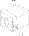
- the printer 700 includes a power supply casing 200 therein.
- the power supply casing 200 is a box-shaped member specified by a dotted line and includes the power device 100 therein.
- the power device 100 includes a circuit board 201 specified by a dash-dot-dash line and the primary electrolytic capacitor 105 mounted on the circuit board 201. As described above, the power device 100 further includes various other electric elements, but illustrations thereof are omitted in Fig. 3 .
- the circuit board 201 is situated substantially perpendicularly to a horizontal plane, and a surface of the circuit board 201 extends substantially parallel to an XZ plane.
- the circuit board 201 is also fixed to an inner wall of the power supply casing 200 with screws 153.
- the primary electrolytic capacitor 105 is mounted on the circuit board 201 such that the electrolytic capacitor 105 protrudes toward a negative side in the Y-direction.
- the commercial power supply 101 (illustrated in Fig. 2 ) is connected to an inlet 110 via a power supply cable (not illustrated), and the inlet 110 is connected to the power device 100 via cables 111.
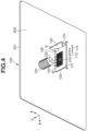
- Fig. 4 is a perspective view illustrating a configuration of the power device 100 according to the present exemplary embodiment. Only major components are illustrated in Fig. 4 .
- the circuit board 201 includes the primary electrolytic capacitor 105, the diode bridge 104, a heatsink 109 (plate-shaped member), and jumper wires 112 and 113 (electric elements) in this order from the top in the Z-direction.
- a surface of the circuit board 201 on the negative side in the Y-direction on which the foregoing components are mounted is referred to as a mounting surface 205.
- the diode bridge 104 among the components on the circuit board 201 is likely to generate heat, and therefore the diode bridge 104 is mounted directly on the heatsink 109 to be in contact with the heatsink 109.
- the jumper wires 112 and 113 are electric elements for pattern wiring of the circuit board 201.
- the jumper wire 112 has a potential equal to the potential DCL
- the jumper wire 113 has a potential equal to the potential DCH.
- the primary electrolytic capacitor 105 protrudes toward the negative side in the Y-direction, and an explosion-proof valve 120 (also referred to as "pressure valve") is provided to a distal end of the primary electrolytic capacitor 105.
- an explosion-proof valve 120 also referred to as "pressure valve”
- the explosion-proof valve 120 opens and releases gas containing an electrolyte outwardly, whereby an increase in pressure in the primary electrolytic capacitor 105 is prevented.
- the electrolyte is a conductive liquid
- adhesion of the electrolyte to a path between the jumper wires 112 and 113 may cause a short circuit at the path, and this may cause an excessive current to flow.
- adhesion of the electrolyte to electronic components such as the jumper wires 112 and 113 needs to be prevented.
- the heatsink 109 between the primary electrolytic capacitor 105 and the jumper wires 112 and 113 in the vertical direction has a devised shape in the configuration according to the present exemplary embodiment.
- the heatsink 109 includes a cutout 130.
- the cutout 130 is formed in a side 133 near the circuit board 201 in the direction (the negative side in the Y-direction) in which the primary electrolytic capacitor 105 protrudes.
- the heatsink 109 includes one bent portion and surfaces 131 and 132.
- the diode bridge 104 is mounted on the surface 131 (predetermined surface), and the surface 132 intersects the surface 131 substantially perpendicularly to the surface 131.
- the cutout 130 is formed at a bent portion 134 where the two surfaces 131 and 132 intersect.
- the four corners of the surface 131 of the heatsink 109 will be referred to as points A, B, C, and D.
- the point A is positioned at an end portion of the surface 131 on the negative side in the Y-direction and a positive side in the X-direction.
- the point B is positioned at an end portion of the surface 131 on the negative side in the Y-direction and a negative side in the X-direction.
- the point C is positioned at an end portion of the cutout 130 on the negative side in the Y-direction.
- the point D is positioned at an end portion of the surface 131 on a positive side in the Y-direction and the positive side in the X-direction.
- the heatsink 109 is basically mounted substantially perpendicularly to the mounting surface 205 of the circuit board 201. In reality, however, the heatsink 109 may be mounted slightly obliquely to the circuit board 201 within an accuracy variation range. Thus, in the configuration illustrated in Fig. 4 in which the jumper wires 112 and 113 are situated under the point C in the vertical direction, adhesion of the electrolyte to the jumper wires 112 and 113 needs to be prevented regardless of in which direction the heatsink 109 is tilted.
- Figs. 5 to 8 below illustrate states where the heatsink 109 tilted in different directions is mounted.
- Fig. 5 is a view illustrating the power device 100 and the power supply casing 200 as viewed along the mounting surface 205 of the circuit board 201.
- Fig. 5 is a view illustrating the power device 100 and the power supply casing 200 as viewed from the positive side to the negative side in the X-direction.
- Fig. 5 illustrates a state where the explosion-proof valve 120 opens and an electrolyte 114 spurted from the primary electrolytic capacitor 105 is scattered in different directions and adheres to an inner wall 220, which faces the primary electrolytic capacitor 105, of the power supply casing 200 and an upper surface of the heatsink 109.
- the heatsink 109 is tilted with respect to the mounting surface 205, and in Fig.
- a position (the point C) of an end portion of the heatsink 109 that is near the circuit board 201 is lower in the vertical direction than a position (the point B) of another end portion of the heatsink 109 that is on an opposite side from the circuit board 201.
- the heatsink 109 is tilted, so that the electrolyte 114 scattered onto the heatsink 109 flows from the point B to the point C. Since the heatsink 109 includes the cutout 130 (illustrated in Fig. 4 ), the electrolyte 114 falls downward in the vertical direction from the point C. As illustrated in Fig. 5 , a position Y2 of the point C in the Y-direction is farther from the circuit board 201 than a position Y1 of the jumper wires 112 and 113 exposed from the mounting surface 205 in the Y-direction is from the circuit board 201.
- a position of at least part of an area where the cutout 130 is formed is farther in the Y-direction from the mounting surface 205 of the circuit board 201 than the position of the jumper wires 112 and 113 is from the circuit board 201.
- the electrolyte 114 having fallen from the point C falls to a bottom surface of the power supply casing 200 without adhering to the jumper wires 112 and 113.
- the electrolyte 114 that previously falls after being guided to a position near the circuit board 201 falls from a position far from the circuit board 201. This prevents adhesion of the electrolyte 114 to the jumper wires 112 and 113 situated under the primary electrolytic capacitor 105 in the vertical direction.
- Fig. 6 illustrates a state where the heatsink 109 is tilted in a direction opposite to the tilt direction illustrated in Fig. 5 .
- the position (the point C) of the end portion of the heatsink 109 that is near the circuit board 201 is higher in the vertical direction than the position (the point B) of the other end portion of the heatsink 109 that is on the opposite side from the circuit board 201.
- the electrolyte 114 scattered onto the heatsink 109 flows from the point C to the point B, so that the electrolyte 114 falls downward in the vertical direction from the point B in Fig. 6 .
- Fig. 6 illustrates a state where the heatsink 109 is tilted in a direction opposite to the tilt direction illustrated in Fig. 5 .
- the position (the point C) of the end portion of the heatsink 109 that is near the circuit board 201 is higher in the vertical direction than the position (the point B) of the other end portion of the heatsink 109 that is on the
- a position Y4 of the point B in the Y-direction is farther from the circuit board 201 than the position Y1 of the jumper wires 112 and 113 exposed from the mounting surface 205 in the Y-direction is from the circuit board 201.
- the electrolyte 114 having fallen from the point B falls to the bottom surface of the power supply casing 200 without adhering to the jumper wires 112 and 113.
- the position Y4 of the point B in the Y-direction is also farther from the circuit board 201 than a position Y3 of a distal end portion of the primary electrolytic capacitor 105 is from the circuit board 201.
- the heatsink 109 protrudes beyond the primary electrolytic capacitor 105 from the circuit board 201.
- the heatsink 109 plays a role as a kind of an umbrella for the jumper wires 112 and 113 and prevents the electrolyte 114 spurted from the distal end portion of the primary electrolytic capacitor 105 from being reflected by the inner wall 220 and adhering to the jumper wires 112 and 113. This effect is similarly obtained also in the state illustrated in Fig. 5 .
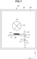
- Fig. 7 is a diagram illustrating the power device 100 as viewed from a direction perpendicular to the mounting surface 205 of the circuit board 201. Specifically, Fig. 7 is a diagram illustrating the power device 100 as viewed from the negative side to the positive side in the Y-direction. Further, as illustrated in Fig. 7 , the surface 131 of the heatsink 109 on which the diode bridge 104 is mounted extends in a direction intersecting the perpendicular direction, and the surface 131 is tilted with respect to the horizontal direction such that the position of the point A is higher in the vertical direction than the position of the point B.
- the electrolyte 114 scattered onto the heatsink 109 flows to a downstream end in the vertical direction, i.e., from the point A to the point B. Since the surface 131 of the heatsink 109 is tilted with respect to the horizontal direction, the electrolyte 114 is guided to the bent portion 134.
- the bent portion 134 is formed by bending the heatsink 109, whereby the electrolyte 114 having flown to the point B is accumulated at the bent portion 134. Thereafter, as illustrated in Fig. 5 or 6 , the electrolyte 114 gathered at the bent portion 134 flows to the point B or C depending on the direction in which the heatsink 109 is tilted. In both states, the electrolyte 114 does not adhere to the jumper wires 112 and 113 as described above with reference to Figs. 5 and 6 .
- Fig. 8 illustrates a state where the heatsink 109 is tilted in a direction opposite to the tilt direction illustrated in Fig. 7 .
- the surface 131 of the heatsink 109 extends in the direction intersecting the perpendicular direction, and the surface 131 is tilted such that the position of the point A is lower in the vertical direction than the position of the point B.
- the electrolyte 114 scattered onto the heatsink 109 flows from the point B to the point A and falls to an area far from the position of the jumper wires 112 and 113 in the X-direction.
- the configuration in which the jumper wires 112 and 113 are provided under the point C in the vertical direction includes the cutout 130 to prevent adhesion of the electrolyte 114 to the electric element regardless of in which direction the heatsink 109 is tilted.
- Figs. 5 to 8 illustrate the heatsink 109 tilted with respect to the mounting surface 205 of the circuit board 201
- the heatsink 109 can be not tilted with respect to the mounting surface 205 and can be substantially perpendicular to the mounting surface 205.
- a cutout can be formed at a position near the point D in a case where the jumper wires 112 and 113 are provided under the point D in the vertical direction. This configuration will be described below.
- Fig. 9 is a perspective view illustrating the power device 100 with the jumper wires 112 and 113 provided under the point D in the vertical direction.
- the heatsink 109 includes not only the cutout 130 but also a cutout 135 near the point D.
- a point E is positioned at an end portion of the cutout 135 on the negative side in the Y-direction.
- the cutout 130 is optional.
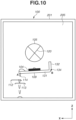
- Fig. 10 is a view illustrating the power device 100 in Fig. 8 as viewed from a direction perpendicular to the mounting surface 205 of the circuit board 201.
- Fig. 10 illustrates a state where the surface 131 of the heatsink 109 is tilted with respect to the horizontal direction due to an effect of accuracy variations. Since the surface 131 is tilted such that the position of the point B is higher in the vertical direction than the position of the point A, the electrolyte 114 scattered onto the heatsink 109 flows from the point B to the point A.
- Fig. 11 is a view illustrating the power device 100 and the power supply casing 200 in Fig. 8 as viewed along the mounting surface 205 of the circuit board 201.
- the electrolyte 114 flows from the point A to the point E. Consequently, the electrolyte 114 falls downward in the vertical direction from the point E.
- a position Y6 of the point E in the Y-direction is farther from the circuit board 201 than a position Y5 of the jumper wires 112 and 113 exposed from the mounting surface 205 in the Y-direction is from the circuit board 201.
- the electrolyte 114 having fallen from the point E falls to the bottom surface of the power supply casing 200 without adhering to the jumper wires 112 and 113.
- the configuration in which the jumper wires 112 and 113 are provided under the point D in the vertical direction includes the cutout 135 to prevent adhesion of the electrolyte 114 to the jumper wires 112 and 113.
- the heatsink 109 can include a hole 136 therein.
- the electrolyte 114 scattered onto the heatsink 109 falls downward in the vertical direction from the hole 136 at a position far from the mounting surface 205 of the circuit board 201.
- This configuration similarly prevents adhesion of the electrolyte 114 to the jumper wires 112 and 113.
- the above-described configurations according to the first exemplary embodiment include a cutout or a hole at the bent portion 134 of the heatsink 109
- aspects of the present invention are not limited to the configurations.
- the cutout 130 is positioned at the bent portion 134, i.e., at the downstream end of the heatsink 109 in the vertical direction that is tilted with respect to the horizontal direction in Fig. 7
- the cutout 130 can be formed at a position that is slightly shifted to the positive side in the X-direction from the bent portion 134.
- the heatsink 109 includes a cutout or a hole to prevent the electrolyte 114 spurted from the primary electrolytic capacitor 105 from adhering to the jumper wires 112 and 113.
- the above-described configurations according to the first exemplary embodiment prevent adhesion of the electrolyte 114 to the jumper wires 112 and 113 using the heatsink 109 mounted on the circuit board 201.
- the power device 100 does not include the heatsink 109.
- a dedicated member for preventing adhesion of the electrolyte 114 to the jumper wires 112 and 113 is intentionally tilted with respect to the mounting surface 205 to be mounted on the mounting surface 205 in the tilted state.
- a basic apparatus configuration of the second exemplary embodiment is similar to that according to the first exemplary embodiment, and thus redundant descriptions thereof are omitted. A configuration that is different from the first exemplary embodiment will be described here.
- Fig. 13 illustrates a configuration of the power device 100 that includes a guide plate 202 (plate-shaped member) for guiding the electrolyte 114.
- Fig. 13 is a diagram illustrating the power device 100 as viewed along the mounting surface 205 of the circuit board 201.
- the guide plate 202 is positioned between the primary electrolytic capacitor 105 and the diode bridge 104 in the Z-direction, and is installed so as to incline in the -Z direction as the distance from the circuit board 201 increases.
- the guide plate 202 is a member for guiding the electrolyte 114 to a position far from the jumper wires 112 and 113.
- the guide plate 202 is, for example, a resin member.
- the guide plate 202 is mounted on the circuit board 201 in a state of being intentionally tilted with respect to the mounting surface 205 rather than being tilted within the accuracy variation range.
- a tilt angle ⁇ of the guide plate 202 with respect to an extension line extending perpendicularly to the mounting surface 205 of the circuit board 201 is desirably 10 degrees or greater.
- the electrolyte 114 having adhered to the guide plate 202 flows to the negative side in the Y-direction and falls in the negative Z-direction from a distal end portion 203 of the guide plate 202 on the negative side in the Y-direction.
- the electrolyte 114 falls to the bottom surface of the power supply casing 200 without adhering to the jumper wires 112 and 113.
- the guide plate 202 for guiding the electrolyte 114 is provided to prevent adhesion of the electrolyte 114 spurted from the primary electrolytic capacitor 105 to the jumper wires 112 and 113 even in a case where a plate-shaped member such as the heatsink 109 is not provided.
- heatsink 109 includes a cutout or a hole in the configurations according to the first exemplary embodiment, aspects of the present invention are not limited to the configurations.
- the guide plate 202 according to the second exemplary embodiment can be provided in place of the heatsink 109, and a cutout or a hole can be formed in the guide plate 202.
- the guide plate 202 is intentionally tilted and mounted on the mounting surface 205 in the configuration according to the second exemplary embodiment, aspects of the present invention are not limited to the configuration.
- the heatsink 109 according to the first exemplary embodiment can be provided in place of the guide plate 202, and the heatsink 109 can be intentionally tilted and mounted on the mounting surface 205.
- the diode bridge 104 is mounted on the heatsink 109 according to the first and second exemplary embodiments, aspects of the present invention are not limited to the configurations.
- the FET 107 which is a switching element, and a rectification diode (not illustrated) of the rectification unit 151 of the secondary circuit are other components that are likely to generate heat, and these components can be in contact with the heatsink 109.
- the jumper wires 112 and 113 are described as an example of an electric element provided under the primary electrolytic capacitor 105 in the vertical direction according to the first and second exemplary embodiments, the two electric elements do not necessarily have to be provided.
- the jumper wire 112 can be provided.
- adhesion of the electrolyte 114 to an area near the jumper wire 112 may cause a short circuit between the jumper wire 112 and the bottom surface of the power supply casing 200 or the ground.
- the heatsink 109 has a predetermined potential, a short circuit may occur between the jumper wire 112 and the heatsink 109.
- the electric element is not limited to the jumper wire 112 and can be another electric element provided to the primary circuit of the transformer 108, such as a resistor or a diode.
Landscapes
- Engineering & Computer Science (AREA)
- Power Engineering (AREA)
- Microelectronics & Electronic Packaging (AREA)
- Physics & Mathematics (AREA)
- General Physics & Mathematics (AREA)
- Thermal Sciences (AREA)
- Dc-Dc Converters (AREA)
- Structures For Mounting Electric Components On Printed Circuit Boards (AREA)
- Electrophotography Configuration And Component (AREA)
- Control Or Security For Electrophotography (AREA)
Abstract
Description
- The present invention relates to an image forming apparatus that includes a power device including an electrolytic capacitor having an explosion-proof valve.
- Power devices that converts commercial alternating current power into direct current power by rectifying and smoothing the commercial alternating current power have been used in image forming apparatuses such as laser beam printers. Such power devices obtain desired output power by inputting the rectified and smoothed direct current power to a transformer and switching the input power, and include a rectification circuit that rectifies input alternating current power and a smoothing circuit that smooths the rectified current.
- The smoothing circuit needs a high-capacitance capacitor, so that an electrolytic capacitor is sometimes used. Application of an excessive voltage to the electrolytic capacitor causes gas to be generated inside the capacitor. In order to prevent an increase in pressure in the capacitor due to the gas, the electrolytic capacitor includes a cutout referred to as an explosion-proof valve (also referred to as "pressure valve"). In a case where the explosion-proof valve operates, the gas containing an electrolyte spurts outwardly from the inside of the capacitor. The spurted electrolyte is a conductive liquid, so that adhesion of the electrolyte to a nearby circuit may affect the circuit. Specifically, in a case where the electrolyte adheres to a primary circuit, a short circuit may occur, and this may cause a high current to flow.
- Considering such an
issue, Japanese Patent No. 6598511 - According to
Japanese Patent No. 6598511 - With the configuration discussed in
Japanese Patent No. 6598511 - The present invention is directed to preventing adhesion of an electrolyte spurted from an electrolytic capacitor to an electric element provided under an electrolytic capacitor in a vertical direction.
- According to an aspect of the present invention, there is provided an image forming apparatus as specified in claims 1 to 6, 11 and 12.
- According to another aspect of the present invention, there is provided an image forming apparatus as specified in claims 7 to 12.
- Further features of the present invention will become apparent from the following description of exemplary embodiments with reference to the attached drawings.
-
-
Fig. 1 is an overall schematic view illustrating a laser beam printer. -
Fig. 2 is a circuit block diagram illustrating a power device. -
Fig. 3 is a view illustrating a layout and a configuration of the power device in the laser beam printer. -
Fig. 4 is a perspective view illustrating the power device including a heatsink with a cutout according to a first exemplary embodiment. -
Fig. 5 is a cross-sectional view illustrating the power device with an electrolyte falling down from a point C. -
Fig. 6 is a cross-sectional view illustrating the power device with the electrolyte falling down from a point B. -
Fig. 7 is a front view illustrating the power device with the heatsink tilted toward the point B. -
Fig. 8 is a front view illustrating the power device with the heatsink tilted toward the point A. -
Fig. 9 is a perspective view illustrating the power device including the heatsink with a new cutout according to the first exemplary embodiment. -
Fig. 10 is a front view illustrating the power device with the heatsink tilted toward the point A. -
Fig. 11 is a cross-sectional view illustrating the power device with the electrolyte falling down from a point E. -
Fig. 12 is a perspective view illustrating the power device including the heatsink with a hole according to the first exemplary embodiment. -
Fig. 13 is a cross-sectional view of a power device including a guide plate according to a second exemplary embodiment. - A
power device 100 according to a first exemplary embodiment of the present invention that is applied to an image forming apparatus will now be described.Fig. 1 is an overall view illustrating a laser beam printer 700 (hereinafter, referred to as "printer 700") as an example of an image forming apparatus. Theprinter 700 includes aphotosensitive drum 701, acharging device 702, and adevelopment device 703. Thephotosensitive drum 701 is an image bearing member on which an electrostatic latent image is to be formed. Thecharging device 702 uniformly charges thephotosensitive drum 701. Thedevelopment device 703 develops an electrostatic latent image formed on thephotosensitive drum 701 using toner. A toner image developed on thephotosensitive drum 701 is transferred at atransfer portion 705 to a sheet as a recording material fed from acassette 704. The transferred toner image on the sheet is then fixed by afixing device 706 heated by aheater 117. The sheet with the fixed toner image thereon is discharged to asheet discharge tray 707. Theprinter 700 includes thepower device 100 that supplies power to a driving unit, such as a motor, and to acontrol unit 500. Thecontrol unit 500 controls, for example, the above-described image forming operations, conveying sheets, and a temperature of theheater 117. -
Fig. 2 is a circuit block diagram illustrating thepower device 100 according to the first exemplary embodiment. A flyback-type switching power supply will be described here as an example. An alternating-current voltage Vac is supplied from acommercial power supply 101 to thepower device 100. The alternating-current voltage Vac supplied to thepower device 100 is supplied to adiode bridge 104 via afuse 102 and afilter circuit 103. If the alternating-current voltage Vac is rectified by thediode bridge 104, a pulsating current waveform with one side being positive is obtained. The voltage with the pulsating current waveform is smoothed to a substantially direct current by an action of a primaryelectrolytic capacitor 105. A voltage applied to both ends of the primaryelectrolytic capacitor 105 will be referred to as "voltage Vdc". A potential of a positive terminal of the primaryelectrolytic capacitor 105 will be referred to as "potential DCH", and a potential of a negative terminal of the primaryelectrolytic capacitor 105 will be referred to as "potential DCL". - The smoothed voltage Vdc is input to a primary winding Np of a
transformer 108, and is fed back via a field-effect transistor (FET) 107 to thecommercial power supply 101 through the negative terminal of the primaryelectrolytic capacitor 105 and thediode bridge 104. The ON/OFF timings of theFET 107 are controlled by aswitching control unit 106. Before the switching is started, theswitching control unit 106 acquires operation power from a terminal ST, whereas after the switching is started, theswitching control unit 106 acquires operation power from a voltage between terminals VB and VS, which is generated from an auxiliary winding Nb of thetransformer 108. The terminal VS of theswitching control unit 106 is connected to the potential DCL. - A
rectification unit 151 is connected to a secondary winding Ns of thetransformer 108. Power converted to a voltage by thetransformer 108 is fed to therectification unit 151, and therectification unit 151 rectifies and smooths the fed voltage to obtain a direct current voltage Vout. The direct-current voltage Vout is output to aload 152 outside thepower device 100. Theload 152 includes, for example, a central processing unit (CPU) (not illustrated) of thecontrol unit 500 illustrated inFig. 1 and the driving unit such as a motor. The direct-current voltage Vout is connected to avoltage feedback unit 150, and thevoltage feedback unit 150 outputs information indicating whether the direct-current voltage Vout is a predetermined voltage. Specifically, thevoltage feedback unit 150 outputs a voltage as an electric signal between terminals FB and VS of the switchingcontrol unit 106. Thevoltage feedback unit 150 includes primary and secondary circuits insulated from each other, and an element, such as a photocoupler, transmits electric signals from the secondary circuit to the primary circuit. The switchingcontrol unit 106 determines the ON/OFF timings of theFET 107 based on a voltage value between the terminals FB and VS and controls the output voltage Vout to be a predetermined voltage value. - A layout of the
power device 100 in theprinter 700 will now be described with reference toFig. 3 . InFig. 3 , a height direction (direction opposite to the vertical direction) of theprinter 700 placed on a horizontal surface is defined as a Z-direction. A direction that intersects the Z-direction and is parallel to a rotation axis direction (main scan direction) of the photosensitive drum 701 (illustrated inFig. 1 ) is defined as an X-direction. A direction that intersects the X-direction and Z-direction is defined as a Y-direction. The X-, Y-, and Z-directions desirably intersect perpendicularly to each other. The XYZ directions also apply to the subsequent drawings. - As illustrated in
Fig. 3 , theprinter 700 includes apower supply casing 200 therein. Thepower supply casing 200 is a box-shaped member specified by a dotted line and includes thepower device 100 therein. Thepower device 100 includes acircuit board 201 specified by a dash-dot-dash line and the primaryelectrolytic capacitor 105 mounted on thecircuit board 201. As described above, thepower device 100 further includes various other electric elements, but illustrations thereof are omitted inFig. 3 . - The
circuit board 201 is situated substantially perpendicularly to a horizontal plane, and a surface of thecircuit board 201 extends substantially parallel to an XZ plane. Thecircuit board 201 is also fixed to an inner wall of thepower supply casing 200 withscrews 153. The primaryelectrolytic capacitor 105 is mounted on thecircuit board 201 such that theelectrolytic capacitor 105 protrudes toward a negative side in the Y-direction. In contrast, the commercial power supply 101 (illustrated inFig. 2 ) is connected to aninlet 110 via a power supply cable (not illustrated), and theinlet 110 is connected to thepower device 100 viacables 111. -
Fig. 4 is a perspective view illustrating a configuration of thepower device 100 according to the present exemplary embodiment. Only major components are illustrated inFig. 4 . Thecircuit board 201 includes the primaryelectrolytic capacitor 105, thediode bridge 104, a heatsink 109 (plate-shaped member), andjumper wires 112 and 113 (electric elements) in this order from the top in the Z-direction. A surface of thecircuit board 201 on the negative side in the Y-direction on which the foregoing components are mounted is referred to as a mountingsurface 205. Thediode bridge 104 among the components on thecircuit board 201 is likely to generate heat, and therefore thediode bridge 104 is mounted directly on theheatsink 109 to be in contact with theheatsink 109. Thejumper wires circuit board 201. Thejumper wire 112 has a potential equal to the potential DCL, and thejumper wire 113 has a potential equal to the potential DCH. - As described above, the primary
electrolytic capacitor 105 protrudes toward the negative side in the Y-direction, and an explosion-proof valve 120 (also referred to as "pressure valve") is provided to a distal end of the primaryelectrolytic capacitor 105. In a case where a voltage that is higher than or equal to a predetermined value is applied to the primaryelectrolytic capacitor 105 due to an abnormality, the explosion-proof valve 120 opens and releases gas containing an electrolyte outwardly, whereby an increase in pressure in the primaryelectrolytic capacitor 105 is prevented. Since the electrolyte is a conductive liquid, adhesion of the electrolyte to a path between thejumper wires jumper wires - In order to prevent adhesion of the electrolyte to the
jumper wires heatsink 109 between the primaryelectrolytic capacitor 105 and thejumper wires Fig. 4 , theheatsink 109 includes acutout 130. Thecutout 130 is formed in aside 133 near thecircuit board 201 in the direction (the negative side in the Y-direction) in which the primaryelectrolytic capacitor 105 protrudes. Further, theheatsink 109 includes one bent portion and surfaces 131 and 132. Thediode bridge 104 is mounted on the surface 131 (predetermined surface), and thesurface 132 intersects thesurface 131 substantially perpendicularly to thesurface 131. Thecutout 130 is formed at abent portion 134 where the twosurfaces - The four corners of the
surface 131 of theheatsink 109 will be referred to as points A, B, C, and D. The point A is positioned at an end portion of thesurface 131 on the negative side in the Y-direction and a positive side in the X-direction. The point B is positioned at an end portion of thesurface 131 on the negative side in the Y-direction and a negative side in the X-direction. The point C is positioned at an end portion of thecutout 130 on the negative side in the Y-direction. The point D is positioned at an end portion of thesurface 131 on a positive side in the Y-direction and the positive side in the X-direction. - The
heatsink 109 is basically mounted substantially perpendicularly to the mountingsurface 205 of thecircuit board 201. In reality, however, theheatsink 109 may be mounted slightly obliquely to thecircuit board 201 within an accuracy variation range. Thus, in the configuration illustrated inFig. 4 in which thejumper wires jumper wires heatsink 109 is tilted.Figs. 5 to 8 below illustrate states where theheatsink 109 tilted in different directions is mounted. -
Fig. 5 is a view illustrating thepower device 100 and thepower supply casing 200 as viewed along the mountingsurface 205 of thecircuit board 201. Specifically,Fig. 5 is a view illustrating thepower device 100 and thepower supply casing 200 as viewed from the positive side to the negative side in the X-direction.Fig. 5 illustrates a state where the explosion-proof valve 120 opens and anelectrolyte 114 spurted from the primaryelectrolytic capacitor 105 is scattered in different directions and adheres to aninner wall 220, which faces the primaryelectrolytic capacitor 105, of thepower supply casing 200 and an upper surface of theheatsink 109. Theheatsink 109 is tilted with respect to the mountingsurface 205, and inFig. 5 , a position (the point C) of an end portion of theheatsink 109 that is near thecircuit board 201 is lower in the vertical direction than a position (the point B) of another end portion of theheatsink 109 that is on an opposite side from thecircuit board 201. - In
Fig. 5 , theheatsink 109 is tilted, so that theelectrolyte 114 scattered onto theheatsink 109 flows from the point B to the point C. Since theheatsink 109 includes the cutout 130 (illustrated inFig. 4 ), theelectrolyte 114 falls downward in the vertical direction from the point C. As illustrated inFig. 5 , a position Y2 of the point C in the Y-direction is farther from thecircuit board 201 than a position Y1 of thejumper wires surface 205 in the Y-direction is from thecircuit board 201. Specifically, a position of at least part of an area where thecutout 130 is formed is farther in the Y-direction from the mountingsurface 205 of thecircuit board 201 than the position of thejumper wires circuit board 201. Thus, theelectrolyte 114 having fallen from the point C falls to a bottom surface of thepower supply casing 200 without adhering to thejumper wires - Specifically, with the
cutout 130, theelectrolyte 114 that previously falls after being guided to a position near thecircuit board 201 falls from a position far from thecircuit board 201. This prevents adhesion of theelectrolyte 114 to thejumper wires electrolytic capacitor 105 in the vertical direction. -
Fig. 6 illustrates a state where theheatsink 109 is tilted in a direction opposite to the tilt direction illustrated inFig. 5 . InFig. 6 , the position (the point C) of the end portion of theheatsink 109 that is near thecircuit board 201 is higher in the vertical direction than the position (the point B) of the other end portion of theheatsink 109 that is on the opposite side from thecircuit board 201. In this case, theelectrolyte 114 scattered onto theheatsink 109 flows from the point C to the point B, so that theelectrolyte 114 falls downward in the vertical direction from the point B inFig. 6 . As illustrated inFig. 6 , a position Y4 of the point B in the Y-direction is farther from thecircuit board 201 than the position Y1 of thejumper wires surface 205 in the Y-direction is from thecircuit board 201. Thus, theelectrolyte 114 having fallen from the point B falls to the bottom surface of thepower supply casing 200 without adhering to thejumper wires - The position Y4 of the point B in the Y-direction is also farther from the
circuit board 201 than a position Y3 of a distal end portion of the primaryelectrolytic capacitor 105 is from thecircuit board 201. In other words, theheatsink 109 protrudes beyond the primaryelectrolytic capacitor 105 from thecircuit board 201. Thus, theheatsink 109 plays a role as a kind of an umbrella for thejumper wires electrolyte 114 spurted from the distal end portion of the primaryelectrolytic capacitor 105 from being reflected by theinner wall 220 and adhering to thejumper wires Fig. 5 . -
Fig. 7 is a diagram illustrating thepower device 100 as viewed from a direction perpendicular to the mountingsurface 205 of thecircuit board 201. Specifically,Fig. 7 is a diagram illustrating thepower device 100 as viewed from the negative side to the positive side in the Y-direction. Further, as illustrated inFig. 7 , thesurface 131 of theheatsink 109 on which thediode bridge 104 is mounted extends in a direction intersecting the perpendicular direction, and thesurface 131 is tilted with respect to the horizontal direction such that the position of the point A is higher in the vertical direction than the position of the point B. - In this case, the
electrolyte 114 scattered onto theheatsink 109 flows to a downstream end in the vertical direction, i.e., from the point A to the point B. Since thesurface 131 of theheatsink 109 is tilted with respect to the horizontal direction, theelectrolyte 114 is guided to thebent portion 134. Thebent portion 134 is formed by bending theheatsink 109, whereby theelectrolyte 114 having flown to the point B is accumulated at thebent portion 134. Thereafter, as illustrated inFig. 5 or6 , theelectrolyte 114 gathered at thebent portion 134 flows to the point B or C depending on the direction in which theheatsink 109 is tilted. In both states, theelectrolyte 114 does not adhere to thejumper wires Figs. 5 and6 . -
Fig. 8 illustrates a state where theheatsink 109 is tilted in a direction opposite to the tilt direction illustrated inFig. 7 . InFig. 7 , thesurface 131 of theheatsink 109 extends in the direction intersecting the perpendicular direction, and thesurface 131 is tilted such that the position of the point A is lower in the vertical direction than the position of the point B. In this configuration, theelectrolyte 114 scattered onto theheatsink 109 flows from the point B to the point A and falls to an area far from the position of thejumper wires - The above prevents adhesion of the
electrolyte 114 to thejumper wires - As described above, the configuration in which the
jumper wires cutout 130 to prevent adhesion of theelectrolyte 114 to the electric element regardless of in which direction theheatsink 109 is tilted. - While
Figs. 5 to 8 illustrate theheatsink 109 tilted with respect to the mountingsurface 205 of thecircuit board 201, theheatsink 109 can be not tilted with respect to the mountingsurface 205 and can be substantially perpendicular to the mountingsurface 205. - While the
jumper wires jumper wires -
Fig. 9 is a perspective view illustrating thepower device 100 with thejumper wires heatsink 109 includes not only thecutout 130 but also acutout 135 near the point D. A point E is positioned at an end portion of thecutout 135 on the negative side in the Y-direction. Thecutout 130 is optional. -
Fig. 10 is a view illustrating thepower device 100 inFig. 8 as viewed from a direction perpendicular to the mountingsurface 205 of thecircuit board 201.Fig. 10 illustrates a state where thesurface 131 of theheatsink 109 is tilted with respect to the horizontal direction due to an effect of accuracy variations. Since thesurface 131 is tilted such that the position of the point B is higher in the vertical direction than the position of the point A, theelectrolyte 114 scattered onto theheatsink 109 flows from the point B to the point A. -
Fig. 11 is a view illustrating thepower device 100 and thepower supply casing 200 inFig. 8 as viewed along the mountingsurface 205 of thecircuit board 201. In the configuration illustrated inFig. 10 , since the position of the point E is lower in the vertical direction than the position of the point A, theelectrolyte 114 flows from the point A to the point E. Consequently, theelectrolyte 114 falls downward in the vertical direction from the point E. A position Y6 of the point E in the Y-direction is farther from thecircuit board 201 than a position Y5 of thejumper wires surface 205 in the Y-direction is from thecircuit board 201. Thus, theelectrolyte 114 having fallen from the point E falls to the bottom surface of thepower supply casing 200 without adhering to thejumper wires - The state where the
heatsink 109 is tilted and mounted in a direction different from the tilt directions illustrated inFigs. 10 and11 is similar to those described above with reference toFigs. 5 to 8 , and therefore redundant descriptions thereof are omitted. - As described above, the configuration in which the
jumper wires cutout 135 to prevent adhesion of theelectrolyte 114 to thejumper wires - While the cutouts are formed in the end portions of the
heatsink 109 in the above-described configurations according to the first exemplary embodiment, aspects of the present invention are not limited to the configurations described above. As illustrated inFig. 12 , theheatsink 109 can include ahole 136 therein. Theelectrolyte 114 scattered onto theheatsink 109 falls downward in the vertical direction from thehole 136 at a position far from the mountingsurface 205 of thecircuit board 201. This configuration similarly prevents adhesion of theelectrolyte 114 to thejumper wires - Further, while the above-described configurations according to the first exemplary embodiment include a cutout or a hole at the
bent portion 134 of theheatsink 109, aspects of the present invention are not limited to the configurations. For example, while thecutout 130 is positioned at thebent portion 134, i.e., at the downstream end of theheatsink 109 in the vertical direction that is tilted with respect to the horizontal direction inFig. 7 , thecutout 130 can be formed at a position that is slightly shifted to the positive side in the X-direction from thebent portion 134. - As described above, according to the present exemplary embodiment, the
heatsink 109 includes a cutout or a hole to prevent theelectrolyte 114 spurted from the primaryelectrolytic capacitor 105 from adhering to thejumper wires - The above-described configurations according to the first exemplary embodiment prevent adhesion of the
electrolyte 114 to thejumper wires heatsink 109 mounted on thecircuit board 201. However, there may be a case where thepower device 100 does not include theheatsink 109. - According to a second exemplary embodiment, a dedicated member for preventing adhesion of the
electrolyte 114 to thejumper wires surface 205 to be mounted on the mountingsurface 205 in the tilted state. A basic apparatus configuration of the second exemplary embodiment is similar to that according to the first exemplary embodiment, and thus redundant descriptions thereof are omitted. A configuration that is different from the first exemplary embodiment will be described here. -
Fig. 13 illustrates a configuration of thepower device 100 that includes a guide plate 202 (plate-shaped member) for guiding theelectrolyte 114.Fig. 13 is a diagram illustrating thepower device 100 as viewed along the mountingsurface 205 of thecircuit board 201. InFig. 13 , theguide plate 202 is positioned between the primaryelectrolytic capacitor 105 and thediode bridge 104 in the Z-direction, and is installed so as to incline in the -Z direction as the distance from thecircuit board 201 increases. - The
guide plate 202 is a member for guiding theelectrolyte 114 to a position far from thejumper wires guide plate 202 is, for example, a resin member. Further, theguide plate 202 is mounted on thecircuit board 201 in a state of being intentionally tilted with respect to the mountingsurface 205 rather than being tilted within the accuracy variation range. Specifically, a tilt angle θ of theguide plate 202 with respect to an extension line extending perpendicularly to the mountingsurface 205 of thecircuit board 201 is desirably 10 degrees or greater. - In this configuration, the
electrolyte 114 having adhered to theguide plate 202 flows to the negative side in the Y-direction and falls in the negative Z-direction from adistal end portion 203 of theguide plate 202 on the negative side in the Y-direction. Thus, theelectrolyte 114 falls to the bottom surface of thepower supply casing 200 without adhering to thejumper wires - As described above, according to the present exemplary embodiment, the
guide plate 202 for guiding theelectrolyte 114 is provided to prevent adhesion of theelectrolyte 114 spurted from the primaryelectrolytic capacitor 105 to thejumper wires heatsink 109 is not provided. - While the
heatsink 109 includes a cutout or a hole in the configurations according to the first exemplary embodiment, aspects of the present invention are not limited to the configurations. Theguide plate 202 according to the second exemplary embodiment can be provided in place of theheatsink 109, and a cutout or a hole can be formed in theguide plate 202. - Further, while the
guide plate 202 is intentionally tilted and mounted on the mountingsurface 205 in the configuration according to the second exemplary embodiment, aspects of the present invention are not limited to the configuration. Theheatsink 109 according to the first exemplary embodiment can be provided in place of theguide plate 202, and theheatsink 109 can be intentionally tilted and mounted on the mountingsurface 205. - Further, while the
diode bridge 104 is mounted on theheatsink 109 according to the first and second exemplary embodiments, aspects of the present invention are not limited to the configurations. TheFET 107, which is a switching element, and a rectification diode (not illustrated) of therectification unit 151 of the secondary circuit are other components that are likely to generate heat, and these components can be in contact with theheatsink 109. - While the
jumper wires electrolytic capacitor 105 in the vertical direction according to the first and second exemplary embodiments, the two electric elements do not necessarily have to be provided. For example, only thejumper wire 112 can be provided. In this case, adhesion of theelectrolyte 114 to an area near thejumper wire 112 may cause a short circuit between thejumper wire 112 and the bottom surface of thepower supply casing 200 or the ground. Further, since theheatsink 109 has a predetermined potential, a short circuit may occur between thejumper wire 112 and theheatsink 109. Furthermore, the electric element is not limited to thejumper wire 112 and can be another electric element provided to the primary circuit of thetransformer 108, such as a resistor or a diode. - While the present invention has been described with reference to exemplary embodiments, it is to be understood that the invention is not limited to the disclosed exemplary embodiments. The following claims define the scope of the invention.
Claims (12)
- An image forming apparatus comprising: image forming means for forming an image on a recording material; anda power device (100) for supplying power to the image forming means, the power device including a circuit board (201) provided to intersect a horizontal plane (X),wherein the power device includes:an electrolytic capacitor (105) including an explosion-proof valve (120) for opening and spurting an inside electrolyte outwardly in a case where a voltage higher than or equal to a predetermined value is applied, the electrolytic capacitor protruding in a first direction (Y) from a mounting surface (205) of the circuit board;an electric element (112, 113) under the electrolytic capacitor in a vertical direction (Z), the electric element being exposed from the mounting surface; anda plate-shaped member (109) provided between the electrolytic capacitor and the electric element in the vertical direction, the plate-shaped member including a first surface (131) extending in a second direction (X) intersecting the vertical direction as viewed in a direction perpendicular to the mounting surface of the circuit board,wherein the plate-shaped member includes a cutout or a hole (130), and a position of at least part of an area where the cutout or the hole is formed is farther in the first direction (Y) from the mounting surface of the circuit board than a position of the electric element.
- The image forming apparatus according to claim 1, wherein the plate-shaped member includes the cutout formed in a side nearest the circuit board in the first direction, and a position of an end portion of the cutout that is on an opposite side from the circuit board is farther in the first direction from the mounting surface of the circuit board than the position of the electric element is.
- The image forming apparatus according to claim 1 or 2, wherein the plate-shaped member includes at least one bent portion and includes a second surface intersecting the first surface besides the first surface, and the cutout or the hole is formed at the bent portion where the first surface and the second surface intersect.
- The image forming apparatus according to any one of claims 1 to 3, wherein the second direction is tilted with respect to a horizontal direction as viewed from the direction perpendicular to the mounting surface of the circuit board, and the cutout or the hole is formed in a downstream end of the plate-shaped member in the vertical direction.
- The image forming apparatus according to any one of claims 1 to 4, wherein the plate-shaped member is tilted with respect to the mounting surface such that, as viewed along the mounting surface of the circuit board, a position of an end portion of the plate-shaped member that is nearest the circuit board in the first direction is lower in the vertical direction than a position of another end portion of the plate-shaped member that is on an opposite side from the circuit board.
- The image forming apparatus according to any one of claims 1 to 5, wherein the plate-shaped member protrudes beyond a distal end portion of the electrolytic capacitor in the first direction as viewed along the mounting surface of the circuit board.
- An image forming apparatus comprising:image forming means for forming an image on a recording material; anda power device (100) for supplying power to the image forming means, the power device including a circuit board (201) provided to intersect a horizontal plane (X),wherein the power device includes:an electrolytic capacitor (105) including an explosion-proof valve (120) for opening and spurting an inside electrolyte outwardly in a case where a voltage higher than or equal to a predetermined value is applied, the electrolytic capacitor protruding in a first direction (Y) from a mounting surface (205) of the circuit board;an electric element (112, 113) under the electrolytic capacitor in a vertical direction (Z), the electric element being exposed from the mounting surface; anda plate-shaped member (109) provided between the electrolytic capacitor and the electric element in the vertical direction, the plate-shaped member including a first surface (131) extending in a second direction (X) intersecting the vertical direction as viewed in a direction perpendicular to the mounting surface of the circuit board,wherein the plate-shaped member protrudes beyond a distal end portion (Y3) of the electrolytic capacitor in the first direction as viewed along the mounting surface of the circuit board, and the plate-shaped member is tilted with respect to the mounting surface such that, as viewed along the mounting surface of the circuit board, a position of an end portion (C) of the plate-shaped member that is nearest the circuit board in the first direction is higher in the vertical direction than a position of another end portion (B) of the plate-shaped member that is on an opposite side from the circuit board.
- The image forming apparatus according to claim 7, wherein the plate-shaped member is tilted by greater than or equal to 10 degrees with respect to the direction perpendicular to the mounting surface of the circuit board.
- The image forming apparatus according to any one of claims 1 to 8, the plate-shaped member is a heatsink for releasing heat from the power device.
- The image forming apparatus according to claim 9, further comprising a diode bridge for converting an alternating current supplied from a commercial power supply into a direct current,
wherein the diode bridge is in contact with the heatsink. - The image forming apparatus according to any one of claims 1 to 10, wherein the plate-shaped member is a guide plate for guiding the electrolyte in a predetermined direction.
- The image forming apparatus according to any one of claims 1 to 11, further comprising a transformer (108) having a primary winding (Np) and a secondary winding (Ns) and outputting a voltage to the secondary winding in accordance with a voltage input to the primary winding,
wherein the electric element is a jumper wire (112, 113) provided to a primary circuit of the transformer.
Applications Claiming Priority (1)
| Application Number | Priority Date | Filing Date | Title |
|---|---|---|---|
| JP2021172313A JP7739132B2 (en) | 2021-10-21 | 2021-10-21 | Image forming device |
Publications (2)
| Publication Number | Publication Date |
|---|---|
| EP4170432A1 true EP4170432A1 (en) | 2023-04-26 |
| EP4170432B1 EP4170432B1 (en) | 2024-09-04 |
Family
ID=83903058
Family Applications (1)
| Application Number | Title | Priority Date | Filing Date |
|---|---|---|---|
| EP22202829.2A Active EP4170432B1 (en) | 2021-10-21 | 2022-10-20 | Image forming apparatus |
Country Status (4)
| Country | Link |
|---|---|
| US (1) | US11842858B2 (en) |
| EP (1) | EP4170432B1 (en) |
| JP (1) | JP7739132B2 (en) |
| CN (1) | CN116009369A (en) |
Citations (4)
| Publication number | Priority date | Publication date | Assignee | Title |
|---|---|---|---|---|
| JP2015189190A (en) * | 2014-03-28 | 2015-11-02 | キヤノン株式会社 | Power supply unit and image formation apparatus |
| JP2017044817A (en) * | 2015-08-25 | 2017-03-02 | 京セラドキュメントソリューションズ株式会社 | Image forming apparatus |
| JP2017076725A (en) * | 2015-10-15 | 2017-04-20 | 京セラドキュメントソリューションズ株式会社 | Power supply device and image forming device |
| JP6598511B2 (en) | 2015-05-21 | 2019-10-30 | キヤノン株式会社 | Power supply device and image forming apparatus |
Family Cites Families (4)
| Publication number | Priority date | Publication date | Assignee | Title |
|---|---|---|---|---|
| JP2004281652A (en) * | 2003-03-14 | 2004-10-07 | Matsushita Electric Ind Co Ltd | Power control device |
| JP5743276B2 (en) | 2011-09-26 | 2015-07-01 | Fdk株式会社 | Battery unit |
| WO2018088162A1 (en) * | 2016-11-11 | 2018-05-17 | 日本精工株式会社 | Electronic control device and steering device |
| JP2021018304A (en) * | 2019-07-19 | 2021-02-15 | キヤノン株式会社 | Electrical apparatus having power supply circuit board |
-
2021
- 2021-10-21 JP JP2021172313A patent/JP7739132B2/en active Active
-
2022
- 2022-10-18 US US18/047,436 patent/US11842858B2/en active Active
- 2022-10-19 CN CN202211278061.5A patent/CN116009369A/en active Pending
- 2022-10-20 EP EP22202829.2A patent/EP4170432B1/en active Active
Patent Citations (4)
| Publication number | Priority date | Publication date | Assignee | Title |
|---|---|---|---|---|
| JP2015189190A (en) * | 2014-03-28 | 2015-11-02 | キヤノン株式会社 | Power supply unit and image formation apparatus |
| JP6598511B2 (en) | 2015-05-21 | 2019-10-30 | キヤノン株式会社 | Power supply device and image forming apparatus |
| JP2017044817A (en) * | 2015-08-25 | 2017-03-02 | 京セラドキュメントソリューションズ株式会社 | Image forming apparatus |
| JP2017076725A (en) * | 2015-10-15 | 2017-04-20 | 京セラドキュメントソリューションズ株式会社 | Power supply device and image forming device |
Also Published As
| Publication number | Publication date |
|---|---|
| CN116009369A (en) | 2023-04-25 |
| JP2023062377A (en) | 2023-05-08 |
| EP4170432B1 (en) | 2024-09-04 |
| US11842858B2 (en) | 2023-12-12 |
| US20230131664A1 (en) | 2023-04-27 |
| JP7739132B2 (en) | 2025-09-16 |
Similar Documents
| Publication | Publication Date | Title |
|---|---|---|
| CN103001497B (en) | Supply unit and image processing system | |
| CN103166484B (en) | Comprise power supply and the image forming apparatus of zero cross detection circuit | |
| JP5966623B2 (en) | Image forming apparatus | |
| EP4170432B1 (en) | Image forming apparatus | |
| US12107506B2 (en) | Power supply apparatus and image forming apparatus | |
| JP2016220420A (en) | Power supply device and image forming apparatus | |
| JP6501449B2 (en) | Power supply device and image forming apparatus | |
| KR20220001479A (en) | Image forming apparatus | |
| US11809119B2 (en) | Power supply apparatus and image forming apparatus | |
| JP6241306B2 (en) | Circuit board, image forming apparatus including the board, and circuit board error detection method | |
| US12429794B2 (en) | Image forming apparatus | |
| JP6748483B2 (en) | Converter and image forming apparatus including converter | |
| JP7589026B2 (en) | Power supply device and image forming apparatus | |
| JP3000732B2 (en) | Corona discharge device | |
| US20250175086A1 (en) | Power supply substrate and image forming apparatus | |
| US20240291926A1 (en) | Circuit board and image forming apparatus | |
| JP7301600B2 (en) | Power supply and image forming apparatus | |
| US20190037697A1 (en) | Printed circuit board | |
| US12189322B2 (en) | Image forming apparatus | |
| JP2564707Y2 (en) | Electrophotographic equipment | |
| JP7293942B2 (en) | Power supply and image forming apparatus | |
| JP2024122833A (en) | Circuit boards, image forming devices | |
| JP4423923B2 (en) | Image forming apparatus | |
| JP2005062608A (en) | Transfer device, power supply device, and image forming apparatus having them | |
| JP2025151657A (en) | Power supply circuits, image processing devices |
Legal Events
| Date | Code | Title | Description |
|---|---|---|---|
| PUAI | Public reference made under article 153(3) epc to a published international application that has entered the european phase |
Free format text: ORIGINAL CODE: 0009012 |
|
| STAA | Information on the status of an ep patent application or granted ep patent |
Free format text: STATUS: THE APPLICATION HAS BEEN PUBLISHED |
|
| AK | Designated contracting states |
Kind code of ref document: A1 Designated state(s): AL AT BE BG CH CY CZ DE DK EE ES FI FR GB GR HR HU IE IS IT LI LT LU LV MC ME MK MT NL NO PL PT RO RS SE SI SK SM TR |
|
| STAA | Information on the status of an ep patent application or granted ep patent |
Free format text: STATUS: REQUEST FOR EXAMINATION WAS MADE |
|
| 17P | Request for examination filed |
Effective date: 20231026 |
|
| RBV | Designated contracting states (corrected) |
Designated state(s): AL AT BE BG CH CY CZ DE DK EE ES FI FR GB GR HR HU IE IS IT LI LT LU LV MC ME MK MT NL NO PL PT RO RS SE SI SK SM TR |
|
| GRAP | Despatch of communication of intention to grant a patent |
Free format text: ORIGINAL CODE: EPIDOSNIGR1 |
|
| STAA | Information on the status of an ep patent application or granted ep patent |
Free format text: STATUS: GRANT OF PATENT IS INTENDED |
|
| RIC1 | Information provided on ipc code assigned before grant |
Ipc: H01G 9/12 20060101ALI20240311BHEP Ipc: G03G 21/16 20060101ALI20240311BHEP Ipc: G03G 15/00 20060101AFI20240311BHEP |
|
| INTG | Intention to grant announced |
Effective date: 20240327 |
|
| GRAS | Grant fee paid |
Free format text: ORIGINAL CODE: EPIDOSNIGR3 |
|
| GRAA | (expected) grant |
Free format text: ORIGINAL CODE: 0009210 |
|
| STAA | Information on the status of an ep patent application or granted ep patent |
Free format text: STATUS: THE PATENT HAS BEEN GRANTED |
|
| AK | Designated contracting states |
Kind code of ref document: B1 Designated state(s): AL AT BE BG CH CY CZ DE DK EE ES FI FR GB GR HR HU IE IS IT LI LT LU LV MC ME MK MT NL NO PL PT RO RS SE SI SK SM TR |
|
| REG | Reference to a national code |
Ref country code: GB Ref legal event code: FG4D |
|
| REG | Reference to a national code |
Ref country code: CH Ref legal event code: EP |
|
| REG | Reference to a national code |
Ref country code: IE Ref legal event code: FG4D |
|
| REG | Reference to a national code |
Ref country code: DE Ref legal event code: R096 Ref document number: 602022005859 Country of ref document: DE |
|
| REG | Reference to a national code |
Ref country code: LT Ref legal event code: MG9D |
|
| REG | Reference to a national code |
Ref country code: NL Ref legal event code: MP Effective date: 20240904 |
|
| PG25 | Lapsed in a contracting state [announced via postgrant information from national office to epo] |
Ref country code: NO Free format text: LAPSE BECAUSE OF FAILURE TO SUBMIT A TRANSLATION OF THE DESCRIPTION OR TO PAY THE FEE WITHIN THE PRESCRIBED TIME-LIMIT Effective date: 20241204 |
|
| PG25 | Lapsed in a contracting state [announced via postgrant information from national office to epo] |
Ref country code: GR Free format text: LAPSE BECAUSE OF FAILURE TO SUBMIT A TRANSLATION OF THE DESCRIPTION OR TO PAY THE FEE WITHIN THE PRESCRIBED TIME-LIMIT Effective date: 20241205 Ref country code: FI Free format text: LAPSE BECAUSE OF FAILURE TO SUBMIT A TRANSLATION OF THE DESCRIPTION OR TO PAY THE FEE WITHIN THE PRESCRIBED TIME-LIMIT Effective date: 20240904 |
|
| PG25 | Lapsed in a contracting state [announced via postgrant information from national office to epo] |
Ref country code: BG Free format text: LAPSE BECAUSE OF FAILURE TO SUBMIT A TRANSLATION OF THE DESCRIPTION OR TO PAY THE FEE WITHIN THE PRESCRIBED TIME-LIMIT Effective date: 20240904 |
|
| PG25 | Lapsed in a contracting state [announced via postgrant information from national office to epo] |
Ref country code: LV Free format text: LAPSE BECAUSE OF FAILURE TO SUBMIT A TRANSLATION OF THE DESCRIPTION OR TO PAY THE FEE WITHIN THE PRESCRIBED TIME-LIMIT Effective date: 20240904 |
|
| PG25 | Lapsed in a contracting state [announced via postgrant information from national office to epo] |
Ref country code: HR Free format text: LAPSE BECAUSE OF FAILURE TO SUBMIT A TRANSLATION OF THE DESCRIPTION OR TO PAY THE FEE WITHIN THE PRESCRIBED TIME-LIMIT Effective date: 20240904 |
|
| PG25 | Lapsed in a contracting state [announced via postgrant information from national office to epo] |
Ref country code: ES Free format text: LAPSE BECAUSE OF FAILURE TO SUBMIT A TRANSLATION OF THE DESCRIPTION OR TO PAY THE FEE WITHIN THE PRESCRIBED TIME-LIMIT Effective date: 20240904 Ref country code: RS Free format text: LAPSE BECAUSE OF FAILURE TO SUBMIT A TRANSLATION OF THE DESCRIPTION OR TO PAY THE FEE WITHIN THE PRESCRIBED TIME-LIMIT Effective date: 20241204 |
|
| PG25 | Lapsed in a contracting state [announced via postgrant information from national office to epo] |
Ref country code: RS Free format text: LAPSE BECAUSE OF FAILURE TO SUBMIT A TRANSLATION OF THE DESCRIPTION OR TO PAY THE FEE WITHIN THE PRESCRIBED TIME-LIMIT Effective date: 20241204 Ref country code: NO Free format text: LAPSE BECAUSE OF FAILURE TO SUBMIT A TRANSLATION OF THE DESCRIPTION OR TO PAY THE FEE WITHIN THE PRESCRIBED TIME-LIMIT Effective date: 20241204 Ref country code: LV Free format text: LAPSE BECAUSE OF FAILURE TO SUBMIT A TRANSLATION OF THE DESCRIPTION OR TO PAY THE FEE WITHIN THE PRESCRIBED TIME-LIMIT Effective date: 20240904 Ref country code: HR Free format text: LAPSE BECAUSE OF FAILURE TO SUBMIT A TRANSLATION OF THE DESCRIPTION OR TO PAY THE FEE WITHIN THE PRESCRIBED TIME-LIMIT Effective date: 20240904 Ref country code: GR Free format text: LAPSE BECAUSE OF FAILURE TO SUBMIT A TRANSLATION OF THE DESCRIPTION OR TO PAY THE FEE WITHIN THE PRESCRIBED TIME-LIMIT Effective date: 20241205 Ref country code: FI Free format text: LAPSE BECAUSE OF FAILURE TO SUBMIT A TRANSLATION OF THE DESCRIPTION OR TO PAY THE FEE WITHIN THE PRESCRIBED TIME-LIMIT Effective date: 20240904 Ref country code: ES Free format text: LAPSE BECAUSE OF FAILURE TO SUBMIT A TRANSLATION OF THE DESCRIPTION OR TO PAY THE FEE WITHIN THE PRESCRIBED TIME-LIMIT Effective date: 20240904 Ref country code: BG Free format text: LAPSE BECAUSE OF FAILURE TO SUBMIT A TRANSLATION OF THE DESCRIPTION OR TO PAY THE FEE WITHIN THE PRESCRIBED TIME-LIMIT Effective date: 20240904 |
|
| REG | Reference to a national code |
Ref country code: AT Ref legal event code: MK05 Ref document number: 1721006 Country of ref document: AT Kind code of ref document: T Effective date: 20240904 |
|
| PG25 | Lapsed in a contracting state [announced via postgrant information from national office to epo] |
Ref country code: NL Free format text: LAPSE BECAUSE OF FAILURE TO SUBMIT A TRANSLATION OF THE DESCRIPTION OR TO PAY THE FEE WITHIN THE PRESCRIBED TIME-LIMIT Effective date: 20240904 |
|
| PG25 | Lapsed in a contracting state [announced via postgrant information from national office to epo] |
Ref country code: IS Free format text: LAPSE BECAUSE OF FAILURE TO SUBMIT A TRANSLATION OF THE DESCRIPTION OR TO PAY THE FEE WITHIN THE PRESCRIBED TIME-LIMIT Effective date: 20250104 Ref country code: PT Free format text: LAPSE BECAUSE OF FAILURE TO SUBMIT A TRANSLATION OF THE DESCRIPTION OR TO PAY THE FEE WITHIN THE PRESCRIBED TIME-LIMIT Effective date: 20250106 |
|
| PG25 | Lapsed in a contracting state [announced via postgrant information from national office to epo] |
Ref country code: SM Free format text: LAPSE BECAUSE OF FAILURE TO SUBMIT A TRANSLATION OF THE DESCRIPTION OR TO PAY THE FEE WITHIN THE PRESCRIBED TIME-LIMIT Effective date: 20240904 Ref country code: RO Free format text: LAPSE BECAUSE OF FAILURE TO SUBMIT A TRANSLATION OF THE DESCRIPTION OR TO PAY THE FEE WITHIN THE PRESCRIBED TIME-LIMIT Effective date: 20240904 |
|
| PG25 | Lapsed in a contracting state [announced via postgrant information from national office to epo] |
Ref country code: EE Free format text: LAPSE BECAUSE OF FAILURE TO SUBMIT A TRANSLATION OF THE DESCRIPTION OR TO PAY THE FEE WITHIN THE PRESCRIBED TIME-LIMIT Effective date: 20240904 Ref country code: AT Free format text: LAPSE BECAUSE OF FAILURE TO SUBMIT A TRANSLATION OF THE DESCRIPTION OR TO PAY THE FEE WITHIN THE PRESCRIBED TIME-LIMIT Effective date: 20240904 |
|
| PG25 | Lapsed in a contracting state [announced via postgrant information from national office to epo] |
Ref country code: CZ Free format text: LAPSE BECAUSE OF FAILURE TO SUBMIT A TRANSLATION OF THE DESCRIPTION OR TO PAY THE FEE WITHIN THE PRESCRIBED TIME-LIMIT Effective date: 20240904 Ref country code: PL Free format text: LAPSE BECAUSE OF FAILURE TO SUBMIT A TRANSLATION OF THE DESCRIPTION OR TO PAY THE FEE WITHIN THE PRESCRIBED TIME-LIMIT Effective date: 20240904 |
|
| PG25 | Lapsed in a contracting state [announced via postgrant information from national office to epo] |
Ref country code: SK Free format text: LAPSE BECAUSE OF FAILURE TO SUBMIT A TRANSLATION OF THE DESCRIPTION OR TO PAY THE FEE WITHIN THE PRESCRIBED TIME-LIMIT Effective date: 20240904 Ref country code: IT Free format text: LAPSE BECAUSE OF FAILURE TO SUBMIT A TRANSLATION OF THE DESCRIPTION OR TO PAY THE FEE WITHIN THE PRESCRIBED TIME-LIMIT Effective date: 20240904 |
|
| REG | Reference to a national code |
Ref country code: DE Ref legal event code: R097 Ref document number: 602022005859 Country of ref document: DE |
|
| PG25 | Lapsed in a contracting state [announced via postgrant information from national office to epo] |
Ref country code: MC Free format text: LAPSE BECAUSE OF FAILURE TO SUBMIT A TRANSLATION OF THE DESCRIPTION OR TO PAY THE FEE WITHIN THE PRESCRIBED TIME-LIMIT Effective date: 20240904 |
|
| PG25 | Lapsed in a contracting state [announced via postgrant information from national office to epo] |
Ref country code: DK Free format text: LAPSE BECAUSE OF FAILURE TO SUBMIT A TRANSLATION OF THE DESCRIPTION OR TO PAY THE FEE WITHIN THE PRESCRIBED TIME-LIMIT Effective date: 20240904 |
|
| PLBE | No opposition filed within time limit |
Free format text: ORIGINAL CODE: 0009261 |
|
| STAA | Information on the status of an ep patent application or granted ep patent |
Free format text: STATUS: NO OPPOSITION FILED WITHIN TIME LIMIT |
|
| PG25 | Lapsed in a contracting state [announced via postgrant information from national office to epo] |
Ref country code: LU Free format text: LAPSE BECAUSE OF NON-PAYMENT OF DUE FEES Effective date: 20241020 Ref country code: BE Free format text: LAPSE BECAUSE OF NON-PAYMENT OF DUE FEES Effective date: 20241031 |
|
| REG | Reference to a national code |
Ref country code: BE Ref legal event code: MM Effective date: 20241031 |
|
| 26N | No opposition filed |
Effective date: 20250605 |
|
| PG25 | Lapsed in a contracting state [announced via postgrant information from national office to epo] |
Ref country code: SE Free format text: LAPSE BECAUSE OF FAILURE TO SUBMIT A TRANSLATION OF THE DESCRIPTION OR TO PAY THE FEE WITHIN THE PRESCRIBED TIME-LIMIT Effective date: 20240904 |
|
| PG25 | Lapsed in a contracting state [announced via postgrant information from national office to epo] |
Ref country code: FR Free format text: LAPSE BECAUSE OF NON-PAYMENT OF DUE FEES Effective date: 20241104 |
|
| PG25 | Lapsed in a contracting state [announced via postgrant information from national office to epo] |
Ref country code: IE Free format text: LAPSE BECAUSE OF NON-PAYMENT OF DUE FEES Effective date: 20241020 |
|
| PGFP | Annual fee paid to national office [announced via postgrant information from national office to epo] |
Ref country code: DE Payment date: 20250923 Year of fee payment: 4 |
|
| PG25 | Lapsed in a contracting state [announced via postgrant information from national office to epo] |
Ref country code: CY Free format text: LAPSE BECAUSE OF FAILURE TO SUBMIT A TRANSLATION OF THE DESCRIPTION OR TO PAY THE FEE WITHIN THE PRESCRIBED TIME-LIMIT; INVALID AB INITIO Effective date: 20221020 |
|
| PG25 | Lapsed in a contracting state [announced via postgrant information from national office to epo] |
Ref country code: HU Free format text: LAPSE BECAUSE OF FAILURE TO SUBMIT A TRANSLATION OF THE DESCRIPTION OR TO PAY THE FEE WITHIN THE PRESCRIBED TIME-LIMIT; INVALID AB INITIO Effective date: 20221020 |