EP4167284A2 - Halbleitergehäuse mit tsv-chip - Google Patents
Halbleitergehäuse mit tsv-chip Download PDFInfo
- Publication number
- EP4167284A2 EP4167284A2 EP22196063.6A EP22196063A EP4167284A2 EP 4167284 A2 EP4167284 A2 EP 4167284A2 EP 22196063 A EP22196063 A EP 22196063A EP 4167284 A2 EP4167284 A2 EP 4167284A2
- Authority
- EP
- European Patent Office
- Prior art keywords
- substrate
- semiconductor die
- die
- semiconductor
- memory component
- Prior art date
- Legal status (The legal status is an assumption and is not a legal conclusion. Google has not performed a legal analysis and makes no representation as to the accuracy of the status listed.)
- Pending
Links
Images

Classifications
-
- H—ELECTRICITY
- H10—SEMICONDUCTOR DEVICES; ELECTRIC SOLID-STATE DEVICES NOT OTHERWISE PROVIDED FOR
- H10W—GENERIC PACKAGES, INTERCONNECTIONS, CONNECTORS OR OTHER CONSTRUCTIONAL DETAILS OF DEVICES COVERED BY CLASS H10
- H10W20/00—Interconnections in chips, wafers or substrates
- H10W20/20—Interconnections within wafers or substrates, e.g. through-silicon vias [TSV]
-
- H—ELECTRICITY
- H10—SEMICONDUCTOR DEVICES; ELECTRIC SOLID-STATE DEVICES NOT OTHERWISE PROVIDED FOR
- H10W—GENERIC PACKAGES, INTERCONNECTIONS, CONNECTORS OR OTHER CONSTRUCTIONAL DETAILS OF DEVICES COVERED BY CLASS H10
- H10W70/00—Package substrates; Interposers; Redistribution layers [RDL]
- H10W70/60—Insulating or insulated package substrates; Interposers; Redistribution layers
- H10W70/62—Insulating or insulated package substrates; Interposers; Redistribution layers characterised by their interconnections
- H10W70/65—Shapes or dispositions of interconnections
-
- H—ELECTRICITY
- H10—SEMICONDUCTOR DEVICES; ELECTRIC SOLID-STATE DEVICES NOT OTHERWISE PROVIDED FOR
- H10W—GENERIC PACKAGES, INTERCONNECTIONS, CONNECTORS OR OTHER CONSTRUCTIONAL DETAILS OF DEVICES COVERED BY CLASS H10
- H10W90/00—Package configurations
-
- H—ELECTRICITY
- H10—SEMICONDUCTOR DEVICES; ELECTRIC SOLID-STATE DEVICES NOT OTHERWISE PROVIDED FOR
- H10W—GENERIC PACKAGES, INTERCONNECTIONS, CONNECTORS OR OTHER CONSTRUCTIONAL DETAILS OF DEVICES COVERED BY CLASS H10
- H10W90/00—Package configurations
- H10W90/20—Configurations of stacked chips
- H10W90/288—Configurations of stacked chips characterised by arrangements for thermal management of the stacked chips
-
- H—ELECTRICITY
- H10—SEMICONDUCTOR DEVICES; ELECTRIC SOLID-STATE DEVICES NOT OTHERWISE PROVIDED FOR
- H10W—GENERIC PACKAGES, INTERCONNECTIONS, CONNECTORS OR OTHER CONSTRUCTIONAL DETAILS OF DEVICES COVERED BY CLASS H10
- H10W90/00—Package configurations
- H10W90/401—Package configurations characterised by multiple insulating or insulated package substrates, interposers or RDLs
-
- H—ELECTRICITY
- H10—SEMICONDUCTOR DEVICES; ELECTRIC SOLID-STATE DEVICES NOT OTHERWISE PROVIDED FOR
- H10W—GENERIC PACKAGES, INTERCONNECTIONS, CONNECTORS OR OTHER CONSTRUCTIONAL DETAILS OF DEVICES COVERED BY CLASS H10
- H10W90/00—Package configurations
- H10W90/701—Package configurations characterised by the relative positions of pads or connectors relative to package parts
-
- H—ELECTRICITY
- H10—SEMICONDUCTOR DEVICES; ELECTRIC SOLID-STATE DEVICES NOT OTHERWISE PROVIDED FOR
- H10W—GENERIC PACKAGES, INTERCONNECTIONS, CONNECTORS OR OTHER CONSTRUCTIONAL DETAILS OF DEVICES COVERED BY CLASS H10
- H10W70/00—Package substrates; Interposers; Redistribution layers [RDL]
- H10W70/60—Insulating or insulated package substrates; Interposers; Redistribution layers
-
- H—ELECTRICITY
- H10—SEMICONDUCTOR DEVICES; ELECTRIC SOLID-STATE DEVICES NOT OTHERWISE PROVIDED FOR
- H10W—GENERIC PACKAGES, INTERCONNECTIONS, CONNECTORS OR OTHER CONSTRUCTIONAL DETAILS OF DEVICES COVERED BY CLASS H10
- H10W72/00—Interconnections or connectors in packages
- H10W72/071—Connecting or disconnecting
- H10W72/072—Connecting or disconnecting of bump connectors
- H10W72/07251—Connecting or disconnecting of bump connectors characterised by changes in properties of the bump connectors during connecting
- H10W72/07254—Connecting or disconnecting of bump connectors characterised by changes in properties of the bump connectors during connecting changes in dispositions
-
- H—ELECTRICITY
- H10—SEMICONDUCTOR DEVICES; ELECTRIC SOLID-STATE DEVICES NOT OTHERWISE PROVIDED FOR
- H10W—GENERIC PACKAGES, INTERCONNECTIONS, CONNECTORS OR OTHER CONSTRUCTIONAL DETAILS OF DEVICES COVERED BY CLASS H10
- H10W72/00—Interconnections or connectors in packages
- H10W72/20—Bump connectors, e.g. solder bumps or copper pillars; Dummy bumps; Thermal bumps
- H10W72/241—Dispositions, e.g. layouts
- H10W72/244—Dispositions, e.g. layouts relative to underlying supporting features, e.g. bond pads, RDLs or vias
-
- H—ELECTRICITY
- H10—SEMICONDUCTOR DEVICES; ELECTRIC SOLID-STATE DEVICES NOT OTHERWISE PROVIDED FOR
- H10W—GENERIC PACKAGES, INTERCONNECTIONS, CONNECTORS OR OTHER CONSTRUCTIONAL DETAILS OF DEVICES COVERED BY CLASS H10
- H10W72/00—Interconnections or connectors in packages
- H10W72/20—Bump connectors, e.g. solder bumps or copper pillars; Dummy bumps; Thermal bumps
- H10W72/241—Dispositions, e.g. layouts
- H10W72/247—Dispositions of multiple bumps
-
- H—ELECTRICITY
- H10—SEMICONDUCTOR DEVICES; ELECTRIC SOLID-STATE DEVICES NOT OTHERWISE PROVIDED FOR
- H10W—GENERIC PACKAGES, INTERCONNECTIONS, CONNECTORS OR OTHER CONSTRUCTIONAL DETAILS OF DEVICES COVERED BY CLASS H10
- H10W72/00—Interconnections or connectors in packages
- H10W72/823—Interconnections through encapsulations, e.g. pillars through molded resin on a lateral side a chip
-
- H—ELECTRICITY
- H10—SEMICONDUCTOR DEVICES; ELECTRIC SOLID-STATE DEVICES NOT OTHERWISE PROVIDED FOR
- H10W—GENERIC PACKAGES, INTERCONNECTIONS, CONNECTORS OR OTHER CONSTRUCTIONAL DETAILS OF DEVICES COVERED BY CLASS H10
- H10W72/00—Interconnections or connectors in packages
- H10W72/851—Dispositions of multiple connectors or interconnections
- H10W72/874—On different surfaces
- H10W72/877—Bump connectors and die-attach connectors
-
- H—ELECTRICITY
- H10—SEMICONDUCTOR DEVICES; ELECTRIC SOLID-STATE DEVICES NOT OTHERWISE PROVIDED FOR
- H10W—GENERIC PACKAGES, INTERCONNECTIONS, CONNECTORS OR OTHER CONSTRUCTIONAL DETAILS OF DEVICES COVERED BY CLASS H10
- H10W74/00—Encapsulations, e.g. protective coatings
-
- H—ELECTRICITY
- H10—SEMICONDUCTOR DEVICES; ELECTRIC SOLID-STATE DEVICES NOT OTHERWISE PROVIDED FOR
- H10W—GENERIC PACKAGES, INTERCONNECTIONS, CONNECTORS OR OTHER CONSTRUCTIONAL DETAILS OF DEVICES COVERED BY CLASS H10
- H10W74/00—Encapsulations, e.g. protective coatings
- H10W74/10—Encapsulations, e.g. protective coatings characterised by their shape or disposition
- H10W74/111—Encapsulations, e.g. protective coatings characterised by their shape or disposition the semiconductor body being completely enclosed
- H10W74/127—Encapsulations, e.g. protective coatings characterised by their shape or disposition the semiconductor body being completely enclosed characterised by arrangements for sealing or adhesion
-
- H—ELECTRICITY
- H10—SEMICONDUCTOR DEVICES; ELECTRIC SOLID-STATE DEVICES NOT OTHERWISE PROVIDED FOR
- H10W—GENERIC PACKAGES, INTERCONNECTIONS, CONNECTORS OR OTHER CONSTRUCTIONAL DETAILS OF DEVICES COVERED BY CLASS H10
- H10W74/00—Encapsulations, e.g. protective coatings
- H10W74/10—Encapsulations, e.g. protective coatings characterised by their shape or disposition
- H10W74/15—Encapsulations, e.g. protective coatings characterised by their shape or disposition on active surfaces of flip-chip devices, e.g. underfills
-
- H—ELECTRICITY
- H10—SEMICONDUCTOR DEVICES; ELECTRIC SOLID-STATE DEVICES NOT OTHERWISE PROVIDED FOR
- H10W—GENERIC PACKAGES, INTERCONNECTIONS, CONNECTORS OR OTHER CONSTRUCTIONAL DETAILS OF DEVICES COVERED BY CLASS H10
- H10W90/00—Package configurations
- H10W90/20—Configurations of stacked chips
-
- H—ELECTRICITY
- H10—SEMICONDUCTOR DEVICES; ELECTRIC SOLID-STATE DEVICES NOT OTHERWISE PROVIDED FOR
- H10W—GENERIC PACKAGES, INTERCONNECTIONS, CONNECTORS OR OTHER CONSTRUCTIONAL DETAILS OF DEVICES COVERED BY CLASS H10
- H10W90/00—Package configurations
- H10W90/20—Configurations of stacked chips
- H10W90/297—Configurations of stacked chips characterised by the through-semiconductor vias [TSVs] in the stacked chips
-
- H—ELECTRICITY
- H10—SEMICONDUCTOR DEVICES; ELECTRIC SOLID-STATE DEVICES NOT OTHERWISE PROVIDED FOR
- H10W—GENERIC PACKAGES, INTERCONNECTIONS, CONNECTORS OR OTHER CONSTRUCTIONAL DETAILS OF DEVICES COVERED BY CLASS H10
- H10W90/00—Package configurations
- H10W90/701—Package configurations characterised by the relative positions of pads or connectors relative to package parts
- H10W90/721—Package configurations characterised by the relative positions of pads or connectors relative to package parts of bump connectors
- H10W90/722—Package configurations characterised by the relative positions of pads or connectors relative to package parts of bump connectors between stacked chips
-
- H—ELECTRICITY
- H10—SEMICONDUCTOR DEVICES; ELECTRIC SOLID-STATE DEVICES NOT OTHERWISE PROVIDED FOR
- H10W—GENERIC PACKAGES, INTERCONNECTIONS, CONNECTORS OR OTHER CONSTRUCTIONAL DETAILS OF DEVICES COVERED BY CLASS H10
- H10W90/00—Package configurations
- H10W90/701—Package configurations characterised by the relative positions of pads or connectors relative to package parts
- H10W90/721—Package configurations characterised by the relative positions of pads or connectors relative to package parts of bump connectors
- H10W90/724—Package configurations characterised by the relative positions of pads or connectors relative to package parts of bump connectors between a chip and a stacked insulating package substrate, interposer or RDL
-
- H—ELECTRICITY
- H10—SEMICONDUCTOR DEVICES; ELECTRIC SOLID-STATE DEVICES NOT OTHERWISE PROVIDED FOR
- H10W—GENERIC PACKAGES, INTERCONNECTIONS, CONNECTORS OR OTHER CONSTRUCTIONAL DETAILS OF DEVICES COVERED BY CLASS H10
- H10W90/00—Package configurations
- H10W90/701—Package configurations characterised by the relative positions of pads or connectors relative to package parts
- H10W90/731—Package configurations characterised by the relative positions of pads or connectors relative to package parts of die-attach connectors
- H10W90/734—Package configurations characterised by the relative positions of pads or connectors relative to package parts of die-attach connectors between a chip and a stacked insulating package substrate, interposer or RDL
Definitions
- the present disclosure relates generally to the field of semiconductor packaging. More particularly, the present disclosure relates to a semiconductor package with a through-silicon-via (TSV) logic die.
- TSV through-silicon-via
- PoP package-on-package
- HBPoP High-Bandwidth PoP
- Fan-Out PoP Fan-Out PoP
- the logic die and the memory dies are separately packaged. Testability of individual dies is improved because the logic and memory dies can be separately tested, and only known-good-dies, which pass the tests, are packaged. This keeps costs low and allows the ability to customize memory needs for particular processors.
- One object of the present disclosure is to provide an improved semiconductor package with vertically integrated memory die and through-silicon-via (TSV) logic die, which supports very wide I/O interfaces and enables high-bandwidth memory access.
- TSV through-silicon-via
- One aspect of the invention provides a semiconductor package including a bottom package comprising a substrate and a semiconductor die mounted on a top surface of the substrate.
- the semiconductor die has an active surface and a rear surface coupled to the top surface of the substrate.
- the semiconductor die comprises through silicon vias.
- the semiconductor die and the top surface of the substrate are encapsulated by a first molding compound.
- a top package is stacked on the bottom package.
- the top package comprises a memory component.
- a middle re-distribution layer (RDL) structure is disposed between the top package and the bottom package.
- the active surface of the semiconductor die is directly connected to the middle RDL structure through connecting elements.
- the middle RDL structure comprises dielectric layers and interconnect structures.
- the memory component is electrically connected to the substrate via the interconnect structures of the middle RDL structure and the through silicon vias of the semiconductor die.
- the semiconductor die comprises a central processing unit (CPU), a graphics processing unit (GPU), a system-on-a-chip (SOC), a field-programmable gate array (FPGA), a microcontroller unit (MCU), a power management integrated circuit (PMIC) die, a radio frequency (RF) die, a sensor die, a micro-electro-mechanical-system (MEMS) die, or a signal processing die.
- CPU central processing unit
- GPU graphics processing unit
- SOC system-on-a-chip
- FPGA field-programmable gate array
- MCU microcontroller unit
- PMIC power management integrated circuit
- RF radio frequency
- sensor die a sensor die
- MEMS micro-electro-mechanical-system
- the substrate is a re-distribution layer (RDL) substrate.
- RDL re-distribution layer
- the substrate comprises a plurality of connection pads disposed on or near the top surface of the substrate, a plurality of conductive traces interconnecting the plurality of connection pads with a plurality of ball pads distributed on or near a bottom surface of the substrate.
- a plurality of solder balls is disposed on the plurality of ball pads, respectively.
- power or ground to the memory component is provided through the through silicon vias.
- the connecting elements comprises micro-bumps.
- a gap between the middle RDL structure and the active surface of the semiconductor die is filled with an underfill material.
- a plurality of through mold vias is disposed in the first molding compound.
- the memory component is a High-Bandwidth Memory (HBM) including multiple DRAM dies stacked on one another, wherein the stacked DRAM dies are vertically interconnected.
- HBM High-Bandwidth Memory
- the memory component further comprises a DRAM base.
- the DRAM base is electrically coupled to the middle RDL structure, wherein power or ground signals are transmitted to the solder balls on the bottom surface of the substrate via a conductive path comprised of the interconnect structures of the middle RDL structure, the connecting elements, the through silicon vias of the semiconductor die, and the conductive traces of the substrate.
- the semiconductor package further comprises a second molding compound encapsulating the memory component.
- the memory component is aligned with the semiconductor die and disposed at or near the center of the semiconductor die when viewed from above.
- a sidewall of the top package is vertically flush with a sidewall of the bottom package.
- the top package further comprises a dummy die.
- Another aspect of the invention provides a semiconductor package including a substrate and a semiconductor die mounted on a top surface of the substrate in a flip-chip manner.
- the semiconductor die has an active surface and a passive rear surface.
- the semiconductor die comprises through silicon vias.
- a memory component is directly mounted on the semiconductor die.
- the memory component is electrically connected to the semiconductor die through connecting elements.
- the semiconductor die and the memory component are packaged in a unified molding compound.
- the substrate comprises a plurality of conductive traces interconnecting the active surface of the semiconductor die with ball pads distributed on or near a bottom surface of the substrate.
- solder balls are disposed on the ball pads, respectively.
- power or ground signals are transmitted to the solder balls on the bottom surface of the substrate via a conductive path comprised of the connecting elements, the through silicon vias of the semiconductor die, and the conductive traces of the substrate.
- the memory component is a High-Bandwidth Memory (HBM) including multiple DRAM dies stacked on one another, wherein the stacked DRAM dies are vertically interconnected by through silicon vias and microbumps.
- HBM High-Bandwidth Memory
- the memory component further comprises a DRAM base.
- the memory component is offset from a center of the semiconductor die.
- the semiconductor package further comprises a dummy die disposed on the semiconductor die, which is packaged in the unified molding compound.
- Packaging of an integrated circuit (IC) chip can involve attaching the IC chip to a substrate (e.g., a packaging substrate) which, among other things, provides mechanical support and electrical connections between the chip and other electronic components of a device.
- substrate types include, for example, cored substrates, including thin core, thick core (laminate bismaleimide-triazine resin (BT resin) or FR-4 type fibrous board material), and laminate core, as well as coreless substrates.
- Cored package substrates for example, can be built up layer by layer around a central core, with layers of conductive material (usually copper) separated by layers of insulating dielectric, with interlayer connections being formed with through holes or microvias (vias).
- High Bandwidth Memory is a high-speed computer memory interface for 3D-stacked synchronous dynamic random-access memory (SDRAM). HBM achieves higher bandwidth while using less power in a substantially smaller form factor than DDR4 or GDDR5. This is achieved by stacking up to eight DRAM dies and an optional base die which can include buffer circuitry and test logic. The stack is often connected to the memory controller on a GPU or CPU through a substrate, such as a silicon interposer. Alternatively, the memory die could be stacked directly on the CPU or GPU chip. Within the stack the die are vertically interconnected by through-silicon vias (TSVs) and microbumps.
- TSVs through-silicon vias
- the HBM DRAM uses wide-interface architecture to achieve high-speed, low-power operation.
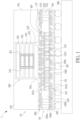
- FIG. 1 is a schematic, cross-sectional diagram showing an exemplary semiconductor package 1 with a TSV die in accordance with one embodiment of the disclosure.
- the semiconductor package 1 may serve as a three-dimensional (3D) semiconductor package assembly including at least two vertically stacked semiconductor dies or chip packages.
- the semiconductor package 1 comprises a bottom package 10 and a top package 30 stacked on the bottom package 10.
- the bottom package 10 may comprise a substrate 100 and a semiconductor die (TSV die) 101, such as a logic die, mounted on a top surface (die-attach surface) 100a of the substrate 100.
- TSV die semiconductor die
- the semiconductor die 101 and the top surface 100a of the substrate 100 may be encapsulated by a molding compound 120.
- the semiconductor package 1 may be mounted on a printed circuit board 500 or any carrier substrate known in the art.
- the semiconductor die 101a may be a central processing unit (CPU), a graphics processing unit (GPU), a system-on-a-chip (SOC), a field-programmable gate array (FPGA), a microcontroller unit (MCU), a power management integrated circuit (PMIC) die, a radio frequency (RF) die, a sensor die, a micro-electro-mechanical-system (MEMS) die, or a signal processing die (e.g., digital signal processing (DSP) die), but is not limited thereto.
- the bottom package 10 may include one or more logic dies.
- the substrate 100 may be a circuit board and may be formed of polymer materials such as bismaleimide triazine (BT) laminates and/or build-up films known in the art.
- the substrate 100 may be a re-distribution layer (RDL) substrate that has a thinner thickness. It is to be understood that the substrate 100 may be a single layer or a multi-layer structure.
- the substrate 100 may comprise a plurality of connection pads lOOp disposed on or near the top surface 100a of the substrate 100.
- the substrate 100 may comprise a plurality of conductive traces lOOt interconnecting the plurality of connection pads lOOp with a plurality of ball pads 100s distributed on or near a bottom surface 100b of the substrate 100.
- Solder balls SB are disposed on the ball pads 100s, respectively.
- at least one passive device PE may be mounted on the bottom surface 100b of the substrate 100 using surface mount technique (SMT).
- SMT surface mount technique
- the semiconductor die 101 is mounted on the top surface 100a of the substrate 100.
- the semiconductor die 101 has a top surface (or active surface) 101a and a passive rear surface 101b.
- the circuit elements such as transistors are fabricated on or near the top surface 101a of the semiconductor die 101.
- the passive rear surface 101b of the semiconductor die 101 may be coupled to the top surface 100a of the substrate 100 by using methods known in the art, for example, SMT or adhesion. That is, the semiconductor die 101 is mounted on the top surface 100a of the substrate 100 with a "face-up" configuration.
- the semiconductor die 101 may be electrically connected to the substrate 100 and the solder balls SB on the bottom surface 100b of the substrate 100 through the through silicon vias (TSVs) 110, which are mainly for power/ground connection of the semiconductor die 101 or HBM.
- TSVs 110 may be power or ground TSVs for transmitting power or ground signals.
- the semiconductor package 1 further comprises a middle re-distribution layer (RDL) structure 200.
- the middle RDL structure 200 may comprise dielectric layers 210 and interconnect structures 220.
- the interconnect structures 220 may be electrically connected to a plurality of RDL pads 230.
- the top surface 101a of the semiconductor die 101 is electrically connected to the middle RDL structure 200 through connecting elements BP such as micro-bumps, metal pillars, or the like.
- the gap between the middle RDL structure 200 and the top surface 101a of the semiconductor die 101 may be filled with an underfill material UF such as an epoxy resin, but is not limited thereto.
- a plurality of through mold vias (TMVs) 122 may be disposed in the molding compound 120.
- the top package 30 is directly stacked on the middle RDL structure 200.
- the top package 30 may comprise a memory component 300 such as a High-Bandwidth Memory (HBM) including multiple DRAM dies 301 stacked on one another and the stacked DRAM dies 301 are vertically interconnected by through silicon vias (TSVs) 310 and microbumps BT.
- the memory component 300 may further comprise a DRAM base 302 which can include buffer circuitry and test logic.
- the DRAM base 302 may include a DRAM controller.
- the top package 30 may further comprise a molding compound 320 encapsulating the memory component 300.
- the sidewall 30s of the top package 30 is vertically flush with the sidewall 20s of the bottom package 10.
- the memory component 300 may be aligned with the underlying semiconductor die 101 and disposed at or near the center of the semiconductor die 101 when viewed from above.
- the center of the memory component 300 may be aligned with the center of the semiconductor die 101.
- the memory component 300 completely overlaps with the underlying semiconductor die 101.
- the DRAM base 302 is electrically coupled to the middle RDL structure 200.
- TSVs 110 of the semiconductor die 101 are provided for power or ground connection to the memory component 300. Power or ground signals may be transmitted to the solder balls SB on the bottom surface 100b of the substrate 100 via the shorter conductive path comprised of the interconnect structures 220 of the middle RDL structure 200, the connecting elements BP, the TSVs 110 of the semiconductor die 101, and the conductive traces lOOt of the substrate 100.
- Signal connection between the memory component 300 and the semiconductor die 101 may be implemented through the middle RDL structure 200. More specifically, signals such as control signals or data signals may be transmitted between the memory component 300 and the semiconductor die 101 through the interconnect structures 220 of the middle RDL structure 200 and the connecting elements BP.
- some of the power or ground signals for the memory component 300 may be transmitted to the solder balls SB on the bottom surface 100b of the substrate 100 via the connecting elements BP, the interconnect structures 220 of the middle RDL structure 200, the TMVs 122, and the conductive traces lOOt of the substrate 100 to reduce the cost of TSV or power via as well as the die area.
- through vias 110v of the semiconductor die 101 are provided for power or ground connection to the circuit devices fabricated in the semiconductor die 101.
- signals transmitted to or from the semiconductor die 101 may be implemented through the connection path comprised of the connecting elements BP, the interconnect structures 220 of the middle RDL structure 200, the TMVs 122, the conductive traces lOOt of the substrate 100, and the solder balls SB on the bottom surface of the 100b of the substrate 100.
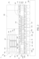
- FIG. 2 is a schematic, cross-sectional diagram showing a variant semiconductor package with a TSV die and a dummy die in accordance with another embodiment of the disclosure, wherein like regions, layers or elements are designated by like numeral numbers or labels.
- the semiconductor package 2 comprises a bottom package 10 and a top package 30 stacked on the bottom package 10.
- the bottom package 10 may comprise a substrate 100 and a semiconductor die 101, such as a logic die, mounted on a top surface 100a of the substrate 100.
- the semiconductor die (TSV die) 101 and the top surface 100a of the substrate 100 may be encapsulated by a molding compound 120.
- the semiconductor die 101a may be a central processing unit (CPU), a graphics processing unit (GPU), a system-on-a-chip (SOC), a field-programmable gate array (FPGA), a microcontroller unit (MCU), a power management integrated circuit (PMIC) die, a radio frequency (RF) die, a sensor die, a micro-electro-mechanical-system (MEMS) die, or a signal processing die (e.g., digital signal processing (DSP) die), but is not limited thereto.
- the bottom package 10 may include one or more logic dies.
- the top package 30 is directly stacked on the middle RDL structure 200.
- the top package 30 may comprise a memory component 300 such as a High-Bandwidth Memory (HBM) including multiple DRAM dies 301 stacked on one another and the stacked DRAM dies 301 are vertically interconnected by through silicon vias (TSVs) 310 and microbumps BT.
- the memory component 300 may further comprise a DRAM base 302 which can include buffer circuitry and test logic.
- the DRAM base 302 may include a DRAM controller.
- the top package 30 may further comprise a molding compound 320 encapsulating the memory component 300.
- the sidewall 30s of the top package 30 is vertically flush with the sidewalls 20s of the bottom package 10.
- the memory component 300 is offset from the center of the underlying semiconductor die 101, Preferably, the center of the memory component 300 is not aligned with and is deviated from the center of the semiconductor die 101. When viewed from above, the memory component 300 may partially overlap with the underlying semiconductor die 101.
- the DRAM base 302 is electrically coupled to the middle RDL structure 200 through the connecting elements 360 such as conductive bumps or micro-bumps.
- the connecting elements 360 are not arranged about a center of the semiconductor die 101.
- all of the connecting elements 360 may be arranged adjacent to an edge of the semiconductor die 101.
- some outer rows of the connecting elements 360, for example, the connecting elements 360e may be disposed beyond an edge of the semiconductor die 101.
- TSVs 110 of the semiconductor die 101 are provided for power or ground connection to the memory component 300.
- Power or ground signals may be transmitted to the solder balls SB on the bottom surface 100b of the substrate 100 via the shorter conductive path comprised of the interconnect structures 220 of the middle RDL structure 200, the connecting elements BP, the TSVs 110 of the semiconductor die 101, and the conductive traces lOOt of the substrate 100.
- Signal connection between the memory component 300 and the semiconductor die 101 may be implemented through the middle RDL structure 200. More specifically, signals such as control signals or data signals may be transmitted between the memory component 300 and the semiconductor die 101 through the interconnect structures 220 of the middle RDL structure 200 and the connecting elements BP.
- some of the power or ground signals for the memory component 300 may be transmitted to the solder balls SB on the bottom surface 100b of the substrate 100 via the connecting elements BP, the interconnect structures 220 of the middle RDL structure 200, the TMVs 122, and the conductive traces lOOt of the substrate 100 to reduce the cost of TSV or power via as well as the die area.
- through vias 110v of the semiconductor die 101 are provided for power or ground connection to the circuit devices fabricated in the semiconductor die 101.
- signals transmitted to or from the semiconductor die 101 may be implemented through the connection path comprised of the connecting elements BP, the interconnect structures 220 of the middle RDL structure 200, the TMVs 122, the conductive traces lOOt of the substrate 100, and the solder balls SB on the bottom surface of the 100b of the substrate 100.
- the top package 30 may further comprise at least one dummy die 400, such as a dummy silicon die.
- the memory component 300 and the dummy die 400 are mounted on the middle RDL structure 200 in a side-by-side manner.
- the dummy die 400 may partially overlap with the underlying semiconductor die 101.
- the off-center configuration of the memory component 300 relative to the underlying semiconductor die 101 allows the placement of the dummy die 400 directly on the semiconductor die 101, which improves the thermal performance of the semiconductor package 2.
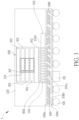
- FIG. 3 is a schematic, cross-sectional diagram showing an exemplary semiconductor package with a TSV die in accordance with still another embodiment of the disclosure, wherein like regions, layers or elements are designated by like numeral numbers or labels.
- the semiconductor package 3 may serve as a 3D semiconductor package assembly including at least two vertically stacked semiconductor dies or chip packages.
- the semiconductor package 3 comprises a substrate 100 and a semiconductor die 101, such as a logic die, mounted on a top surface (die-attach surface) 100a of the substrate 100 in a flip-chip manner.
- the semiconductor die 101 has a top surface (or active surface) 101a and a passive rear surface 101b.
- the circuit elements such as transistors are fabricated on or near the top surface 101a of the semiconductor die 101.
- the substrate 100 may be a RDL substrate that has a thinner thickness. It is to be understood that the substrate 100 may be a single layer or a multi-layer structure. Preferably, for example, the substrate 100 may comprise a plurality of conductive traces lOOt interconnecting the active surface 101a of the semiconductor die 101 with the ball pads 100s distributed on or near the bottom surface 100b of the substrate 100. The solder balls SB are disposed on the ball pads 100s, respectively. Preferably, at least one passive device PE may be mounted on the bottom surface 100b of the substrate 100 using surface mount technique.
- the semiconductor die 101 is mounted on the top surface 100a of the substrate 100 with a "face-down" configuration with its top surface (or active surface) 101a directly facing the substrate 100.
- the semiconductor die 101 may be electrically connected to the substrate 100 and the solder balls SB on the bottom surface 100b of the substrate 100 through the through silicon vias (TSVs) 110, which are mainly for power/ground connection of the semiconductor die 101 or HBM.
- TSVs 110 may be power or ground TSVs for transmitting power or ground signals.
- a memory component 300 such as HBM is directly mounted on the semiconductor die 101.
- the memory component 300 may be electrically connected to the semiconductor die 101 through the connecting elements BM such as micro-bumps or metal pillars.
- the memory component 300 may comprise multiple DRAM dies 301 stacked on one another.
- the stacked DRAM dies 301 are vertically interconnected by through silicon vias (TSVs) 310 and micro-bumps BT.
- the memory component 300 may further comprise a DRAM base 302 which can include buffer circuitry and test logic.
- the DRAM base 302 may include a DRAM controller.
- the semiconductor die 101 and the memory component 300 may be packaged in one unified molding compound 320.
- the semiconductor package 3 may be mounted on a printed circuit board (not shown in this figure) or any carrier substrate known in the art.
- the memory component 300 may be offset from the center of the underlying semiconductor die 101, That is, the center of the memory component 300 is not aligned with and is deviated from the center of the semiconductor die 101.
- signals such as power or ground may be transmitted to the solder balls SB on the bottom surface 100b of the substrate 100 via the shorter conductive path comprised of the connecting elements BM, the TSVs 110 of the semiconductor die 101, and the conductive traces lOOt of the substrate 100.
- the DRAM base 302 may be electrically connected to a middle RDL structure between the semiconductor die 101 and the memory component 300 as described in FIG. 1 .
- FIG. 4 is a schematic, cross-sectional diagram showing an exemplary semiconductor package with a TSV die and a dummy die in accordance with still another embodiment of the disclosure, wherein like regions, layers or elements are designated by like numeral numbers or labels.
- the semiconductor package 4 may serve as a 3D semiconductor package assembly including at least two vertically stacked semiconductor dies or chip packages.
- the semiconductor package 4 comprises a substrate 100 and a semiconductor die 101, such as a logic die, mounted on a top surface (die-attach surface) 100a of the substrate 100 in a flip-chip manner.
- the semiconductor die 101 has a top surface (or active surface) 101a and a passive rear surface 101b.
- the circuit elements such as transistors are fabricated on or near the top surface 101a of the semiconductor die 101.
- the substrate 100 may be a RDL substrate that has a thinner thickness. It is to be understood that the substrate 100 may be a single layer or a multi-layer structure. Preferably, for example, the substrate 100 may comprise a plurality of conductive traces lOOt interconnecting the active surface 101a of the semiconductor die 101 with the ball pads 100s distributed on or near the bottom surface 100b of the substrate 100. The solder balls SB are disposed on the ball pads 100s, respectively. Preferably, at least one passive device PE may be mounted on the bottom surface 100b of the substrate 100 using surface mount technique.
- the semiconductor die 101 is mounted on the top surface 100a of the substrate 100 with a "face-down" configuration with its top surface (or active surface) 101a directly facing the substrate 100.
- the semiconductor die 101 may be electrically connected to the substrate 100 and the solder balls SB on the bottom surface 100b of the substrate 100 through the through silicon vias (TSVs) 110, which are mainly for power/ground connection of the semiconductor die 101 or HBM.
- TSVs 110 may be power or ground TSVs for transmitting power or ground signals.
- the memory component 300 such as HBM is directly mounted on the semiconductor die 101.
- the memory component 300 may be electrically connected to the semiconductor die 101 through the connecting elements BM such as micro-bumps or metal pillars.
- the memory component 300 may comprise multiple DRAM dies 301 stacked on one another.
- the stacked DRAM dies 301 are vertically interconnected by through silicon vias (TSVs) 310 and micro-bumps BT.
- the memory component 300 may further comprise a DRAM base 302 which can include buffer circuitry and test logic.
- the DRAM base 302 may include a DRAM controller.
- the memory component 300 may be offset from the center of the underlying semiconductor die 101, That is, the center of the memory component 300 is not aligned with and is deviated from the center of the semiconductor die 101. When viewed from above, the memory component 300 may only partially overlap with the underlying semiconductor die 101. An off-centered bump or pad design is implemented.
- the connecting elements BM are not arranged about a center of the semiconductor die 101.
- all of the connecting elements BM may be arranged adjacent to an edge of the semiconductor die 101. As shown in FIG. 4 , the memory component 300 may protrude beyond a sidewall of the semiconductor die 101.
- signals such as power or ground may be transmitted to the solder balls SB on the bottom surface 100b of the substrate 100 via the shorter conductive path comprised of the connecting elements BM, the TSVs 110 of the semiconductor die 101, and the conductive traces lOOt of the substrate 100.
- the DRAM base 302 may be electrically connected to a middle RDL structure between the semiconductor die 101 and the memory component 300 as described in FIG. 1 .
- At least one dummy die 400 such as a dummy silicon die is disposed on the semiconductor die 101.
- the dummy die 400 may be mounted to the semiconductor die 101 by using an adhesive layer 410, but is not limited thereto.
- the memory component 300 and the dummy die 400 are mounted on the semiconductor die 101 in a side-by-side manner. When viewed from above, the dummy die 400 may partially overlap with the underlying semiconductor die 101.
- the off-center configuration of the memory component 300 relative to the underlying semiconductor die 101 allows the placement of the dummy die 400 directly on the semiconductor die 101, which improves the thermal performance of the semiconductor package 2.
- the semiconductor die 101, the memory component 300, and the dummy die 400 may be packaged in one unified molding compound 320.
- the semiconductor package 4 may be mounted on a printed circuit board (not shown in this figure) or any carrier substrate known in the art.
Landscapes
- Semiconductor Memories (AREA)
- Semiconductor Integrated Circuits (AREA)
- Internal Circuitry In Semiconductor Integrated Circuit Devices (AREA)
- Physics & Mathematics (AREA)
- Geometry (AREA)
Applications Claiming Priority (2)
| Application Number | Priority Date | Filing Date | Title |
|---|---|---|---|
| US202163255027P | 2021-10-13 | 2021-10-13 | |
| US17/938,911 US20230116326A1 (en) | 2021-10-13 | 2022-09-06 | Semiconductor package with tsv die |
Publications (2)
| Publication Number | Publication Date |
|---|---|
| EP4167284A2 true EP4167284A2 (de) | 2023-04-19 |
| EP4167284A3 EP4167284A3 (de) | 2023-06-07 |
Family
ID=83598444
Family Applications (1)
| Application Number | Title | Priority Date | Filing Date |
|---|---|---|---|
| EP22196063.6A Pending EP4167284A3 (de) | 2021-10-13 | 2022-09-16 | Halbleitergehäuse mit tsv-chip |
Country Status (4)
| Country | Link |
|---|---|
| US (1) | US20230116326A1 (de) |
| EP (1) | EP4167284A3 (de) |
| CN (1) | CN115966558A (de) |
| TW (1) | TWI868490B (de) |
Families Citing this family (11)
| Publication number | Priority date | Publication date | Assignee | Title |
|---|---|---|---|---|
| US9899238B2 (en) * | 2014-12-18 | 2018-02-20 | Intel Corporation | Low cost package warpage solution |
| KR20240048373A (ko) * | 2022-10-06 | 2024-04-15 | 삼성전자주식회사 | 반도체 패키지 |
| KR20240048374A (ko) * | 2022-10-06 | 2024-04-15 | 삼성전자주식회사 | 반도체 패키지 |
| CN119300364A (zh) * | 2023-07-03 | 2025-01-10 | 长鑫存储技术有限公司 | 半导体封装结构 |
| US20250029952A1 (en) * | 2023-07-19 | 2025-01-23 | Avago Technologies International Sales Pte. Limited | Systems and methods for connecting integrated circuits |
| TWI891063B (zh) * | 2023-09-14 | 2025-07-21 | 万閎企業有限公司 | 晶片封裝的製造方法 |
| CN119855165B (zh) * | 2023-10-17 | 2025-10-03 | 长鑫科技集团股份有限公司 | 一种存储芯片、逻辑芯片、芯片堆叠结构和存储器 |
| CN117222234B (zh) * | 2023-11-07 | 2024-02-23 | 北京奎芯集成电路设计有限公司 | 一种基于UCIe接口的半导体器件 |
| US20250192100A1 (en) * | 2023-12-07 | 2025-06-12 | Taiwan Semiconductor Manufacturing Company, Ltd. | System on integrated circuit structure |
| WO2025226352A1 (en) * | 2024-04-25 | 2025-10-30 | Qualcomm Incorporated | Single hybrid system-on-chip (soc) die structure with high memory bandwidth and density |
| CN120957428B (zh) * | 2025-10-14 | 2026-01-30 | 甬矽电子(宁波)股份有限公司 | 半导体封装结构及其封装方法 |
Family Cites Families (9)
| Publication number | Priority date | Publication date | Assignee | Title |
|---|---|---|---|---|
| US9263370B2 (en) * | 2013-09-27 | 2016-02-16 | Qualcomm Mems Technologies, Inc. | Semiconductor device with via bar |
| US10163856B2 (en) * | 2015-10-30 | 2018-12-25 | Taiwan Semiconductor Manufacturing Company, Ltd. | Stacked integrated circuit structure and method of forming |
| US10833052B2 (en) * | 2016-10-06 | 2020-11-10 | Micron Technology, Inc. | Microelectronic package utilizing embedded bridge through-silicon-via interconnect component and related methods |
| US10410969B2 (en) * | 2017-02-15 | 2019-09-10 | Mediatek Inc. | Semiconductor package assembly |
| US10483187B2 (en) * | 2017-06-30 | 2019-11-19 | Taiwan Semiconductor Manufacturing Company, Ltd. | Heat spreading device and method |
| KR102615197B1 (ko) * | 2018-11-23 | 2023-12-18 | 삼성전자주식회사 | 반도체 패키지 |
| US11227846B2 (en) * | 2019-01-30 | 2022-01-18 | Mediatek Inc. | Semiconductor package having improved thermal interface between semiconductor die and heat spreading structure |
| US11133258B2 (en) * | 2019-07-17 | 2021-09-28 | Taiwan Semiconductor Manufacturing Company, Ltd. | Package with bridge die for interconnection and method forming same |
| US12218064B2 (en) * | 2019-08-30 | 2025-02-04 | Intel Corporation | Molded silicon interconnects in bridges for integrated-circuit packages |
-
2022
- 2022-09-06 US US17/938,911 patent/US20230116326A1/en active Pending
- 2022-09-16 EP EP22196063.6A patent/EP4167284A3/de active Pending
- 2022-09-30 TW TW111137133A patent/TWI868490B/zh active
- 2022-10-11 CN CN202211243384.0A patent/CN115966558A/zh active Pending
Also Published As
| Publication number | Publication date |
|---|---|
| TWI868490B (zh) | 2025-01-01 |
| CN115966558A (zh) | 2023-04-14 |
| TW202331992A (zh) | 2023-08-01 |
| US20230116326A1 (en) | 2023-04-13 |
| EP4167284A3 (de) | 2023-06-07 |
Similar Documents
| Publication | Publication Date | Title |
|---|---|---|
| US20230116326A1 (en) | Semiconductor package with tsv die | |
| TWI796831B (zh) | 半導體封裝及其形成方法 | |
| EP4167690B1 (de) | Elektronische vorrichtung mit gestapelten leiterplatten | |
| TWI731239B (zh) | 扇出型半導體封裝 | |
| US10103128B2 (en) | Semiconductor package incorporating redistribution layer interposer | |
| TWI818088B (zh) | 半導體封裝 | |
| US9318467B2 (en) | Multi-die wirebond packages with elongated windows | |
| US12469790B2 (en) | Semiconductor package and method of manufacturing the same | |
| US8592973B2 (en) | Integrated circuit packaging system with package-on-package stacking and method of manufacture thereof | |
| US8269351B2 (en) | Multi-chip stack package structure | |
| US8873245B2 (en) | Embedded chip-on-chip package and package-on-package comprising same | |
| US20230230898A1 (en) | Adhesive and thermal interface material on a plurality of dies covered by a lid | |
| EP3258486A1 (de) | Halbleitergehäuse mit weiterverteilungsschicht-interposer | |
| US9099475B2 (en) | Techniques for reducing inductance in through-die vias of an electronic assembly | |
| US20140252561A1 (en) | Via-enabled package-on-package | |
| TW202013820A (zh) | 天線模組 | |
| CN111063663B (zh) | 双面扇出型系统级封装结构 |
Legal Events
| Date | Code | Title | Description |
|---|---|---|---|
| PUAI | Public reference made under article 153(3) epc to a published international application that has entered the european phase |
Free format text: ORIGINAL CODE: 0009012 |
|
| STAA | Information on the status of an ep patent application or granted ep patent |
Free format text: STATUS: THE APPLICATION HAS BEEN PUBLISHED |
|
| AK | Designated contracting states |
Kind code of ref document: A2 Designated state(s): AL AT BE BG CH CY CZ DE DK EE ES FI FR GB GR HR HU IE IS IT LI LT LU LV MC MK MT NL NO PL PT RO RS SE SI SK SM TR |
|
| PUAL | Search report despatched |
Free format text: ORIGINAL CODE: 0009013 |
|
| AK | Designated contracting states |
Kind code of ref document: A3 Designated state(s): AL AT BE BG CH CY CZ DE DK EE ES FI FR GB GR HR HU IE IS IT LI LT LU LV MC MK MT NL NO PL PT RO RS SE SI SK SM TR |
|
| RIC1 | Information provided on ipc code assigned before grant |
Ipc: H01L 23/00 20060101ALN20230503BHEP Ipc: H01L 25/18 20230101ALI20230503BHEP Ipc: H01L 25/10 20060101AFI20230503BHEP |
|
| P01 | Opt-out of the competence of the unified patent court (upc) registered |
Effective date: 20230607 |
|
| STAA | Information on the status of an ep patent application or granted ep patent |
Free format text: STATUS: REQUEST FOR EXAMINATION WAS MADE |
|
| 17P | Request for examination filed |
Effective date: 20231201 |
|
| RBV | Designated contracting states (corrected) |
Designated state(s): AL AT BE BG CH CY CZ DE DK EE ES FI FR GB GR HR HU IE IS IT LI LT LU LV MC MK MT NL NO PL PT RO RS SE SI SK SM TR |