EP4166940A1 - Gas sensor, method of making the sensor and method of using the sensor - Google Patents
Gas sensor, method of making the sensor and method of using the sensor Download PDFInfo
- Publication number
- EP4166940A1 EP4166940A1 EP22202241.0A EP22202241A EP4166940A1 EP 4166940 A1 EP4166940 A1 EP 4166940A1 EP 22202241 A EP22202241 A EP 22202241A EP 4166940 A1 EP4166940 A1 EP 4166940A1
- Authority
- EP
- European Patent Office
- Prior art keywords
- gas
- metal
- sensing element
- sensing
- disposed
- Prior art date
- Legal status (The legal status is an assumption and is not a legal conclusion. Google has not performed a legal analysis and makes no representation as to the accuracy of the status listed.)
- Granted
Links
Images



Classifications
-
- G—PHYSICS
- G01—MEASURING; TESTING
- G01N—INVESTIGATING OR ANALYSING MATERIALS BY DETERMINING THEIR CHEMICAL OR PHYSICAL PROPERTIES
- G01N27/00—Investigating or analysing materials by the use of electric, electrochemical, or magnetic means
- G01N27/02—Investigating or analysing materials by the use of electric, electrochemical, or magnetic means by investigating impedance
- G01N27/04—Investigating or analysing materials by the use of electric, electrochemical, or magnetic means by investigating impedance by investigating resistance
- G01N27/12—Investigating or analysing materials by the use of electric, electrochemical, or magnetic means by investigating impedance by investigating resistance of a solid body in dependence upon absorption of a fluid; of a solid body in dependence upon reaction with a fluid, for detecting components in the fluid
- G01N27/125—Composition of the body, e.g. the composition of its sensitive layer
-
- C—CHEMISTRY; METALLURGY
- C23—COATING METALLIC MATERIAL; COATING MATERIAL WITH METALLIC MATERIAL; CHEMICAL SURFACE TREATMENT; DIFFUSION TREATMENT OF METALLIC MATERIAL; COATING BY VACUUM EVAPORATION, BY SPUTTERING, BY ION IMPLANTATION OR BY CHEMICAL VAPOUR DEPOSITION, IN GENERAL; INHIBITING CORROSION OF METALLIC MATERIAL OR INCRUSTATION IN GENERAL
- C23C—COATING METALLIC MATERIAL; COATING MATERIAL WITH METALLIC MATERIAL; SURFACE TREATMENT OF METALLIC MATERIAL BY DIFFUSION INTO THE SURFACE, BY CHEMICAL CONVERSION OR SUBSTITUTION; COATING BY VACUUM EVAPORATION, BY SPUTTERING, BY ION IMPLANTATION OR BY CHEMICAL VAPOUR DEPOSITION, IN GENERAL
- C23C14/00—Coating by vacuum evaporation, by sputtering or by ion implantation of the coating forming material
- C23C14/06—Coating by vacuum evaporation, by sputtering or by ion implantation of the coating forming material characterised by the coating material
-
- C—CHEMISTRY; METALLURGY
- C23—COATING METALLIC MATERIAL; COATING MATERIAL WITH METALLIC MATERIAL; CHEMICAL SURFACE TREATMENT; DIFFUSION TREATMENT OF METALLIC MATERIAL; COATING BY VACUUM EVAPORATION, BY SPUTTERING, BY ION IMPLANTATION OR BY CHEMICAL VAPOUR DEPOSITION, IN GENERAL; INHIBITING CORROSION OF METALLIC MATERIAL OR INCRUSTATION IN GENERAL
- C23C—COATING METALLIC MATERIAL; COATING MATERIAL WITH METALLIC MATERIAL; SURFACE TREATMENT OF METALLIC MATERIAL BY DIFFUSION INTO THE SURFACE, BY CHEMICAL CONVERSION OR SUBSTITUTION; COATING BY VACUUM EVAPORATION, BY SPUTTERING, BY ION IMPLANTATION OR BY CHEMICAL VAPOUR DEPOSITION, IN GENERAL
- C23C14/00—Coating by vacuum evaporation, by sputtering or by ion implantation of the coating forming material
- C23C14/06—Coating by vacuum evaporation, by sputtering or by ion implantation of the coating forming material characterised by the coating material
- C23C14/0623—Sulfides, selenides or tellurides
-
- C—CHEMISTRY; METALLURGY
- C23—COATING METALLIC MATERIAL; COATING MATERIAL WITH METALLIC MATERIAL; CHEMICAL SURFACE TREATMENT; DIFFUSION TREATMENT OF METALLIC MATERIAL; COATING BY VACUUM EVAPORATION, BY SPUTTERING, BY ION IMPLANTATION OR BY CHEMICAL VAPOUR DEPOSITION, IN GENERAL; INHIBITING CORROSION OF METALLIC MATERIAL OR INCRUSTATION IN GENERAL
- C23C—COATING METALLIC MATERIAL; COATING MATERIAL WITH METALLIC MATERIAL; SURFACE TREATMENT OF METALLIC MATERIAL BY DIFFUSION INTO THE SURFACE, BY CHEMICAL CONVERSION OR SUBSTITUTION; COATING BY VACUUM EVAPORATION, BY SPUTTERING, BY ION IMPLANTATION OR BY CHEMICAL VAPOUR DEPOSITION, IN GENERAL
- C23C14/00—Coating by vacuum evaporation, by sputtering or by ion implantation of the coating forming material
- C23C14/06—Coating by vacuum evaporation, by sputtering or by ion implantation of the coating forming material characterised by the coating material
- C23C14/0623—Sulfides, selenides or tellurides
- C23C14/0629—Sulfides, selenides or tellurides of zinc, cadmium or mercury
-
- C—CHEMISTRY; METALLURGY
- C23—COATING METALLIC MATERIAL; COATING MATERIAL WITH METALLIC MATERIAL; CHEMICAL SURFACE TREATMENT; DIFFUSION TREATMENT OF METALLIC MATERIAL; COATING BY VACUUM EVAPORATION, BY SPUTTERING, BY ION IMPLANTATION OR BY CHEMICAL VAPOUR DEPOSITION, IN GENERAL; INHIBITING CORROSION OF METALLIC MATERIAL OR INCRUSTATION IN GENERAL
- C23C—COATING METALLIC MATERIAL; COATING MATERIAL WITH METALLIC MATERIAL; SURFACE TREATMENT OF METALLIC MATERIAL BY DIFFUSION INTO THE SURFACE, BY CHEMICAL CONVERSION OR SUBSTITUTION; COATING BY VACUUM EVAPORATION, BY SPUTTERING, BY ION IMPLANTATION OR BY CHEMICAL VAPOUR DEPOSITION, IN GENERAL
- C23C14/00—Coating by vacuum evaporation, by sputtering or by ion implantation of the coating forming material
- C23C14/06—Coating by vacuum evaporation, by sputtering or by ion implantation of the coating forming material characterised by the coating material
- C23C14/08—Oxides
-
- C—CHEMISTRY; METALLURGY
- C23—COATING METALLIC MATERIAL; COATING MATERIAL WITH METALLIC MATERIAL; CHEMICAL SURFACE TREATMENT; DIFFUSION TREATMENT OF METALLIC MATERIAL; COATING BY VACUUM EVAPORATION, BY SPUTTERING, BY ION IMPLANTATION OR BY CHEMICAL VAPOUR DEPOSITION, IN GENERAL; INHIBITING CORROSION OF METALLIC MATERIAL OR INCRUSTATION IN GENERAL
- C23C—COATING METALLIC MATERIAL; COATING MATERIAL WITH METALLIC MATERIAL; SURFACE TREATMENT OF METALLIC MATERIAL BY DIFFUSION INTO THE SURFACE, BY CHEMICAL CONVERSION OR SUBSTITUTION; COATING BY VACUUM EVAPORATION, BY SPUTTERING, BY ION IMPLANTATION OR BY CHEMICAL VAPOUR DEPOSITION, IN GENERAL
- C23C14/00—Coating by vacuum evaporation, by sputtering or by ion implantation of the coating forming material
- C23C14/06—Coating by vacuum evaporation, by sputtering or by ion implantation of the coating forming material characterised by the coating material
- C23C14/08—Oxides
- C23C14/081—Oxides of aluminium, magnesium or beryllium
-
- C—CHEMISTRY; METALLURGY
- C23—COATING METALLIC MATERIAL; COATING MATERIAL WITH METALLIC MATERIAL; CHEMICAL SURFACE TREATMENT; DIFFUSION TREATMENT OF METALLIC MATERIAL; COATING BY VACUUM EVAPORATION, BY SPUTTERING, BY ION IMPLANTATION OR BY CHEMICAL VAPOUR DEPOSITION, IN GENERAL; INHIBITING CORROSION OF METALLIC MATERIAL OR INCRUSTATION IN GENERAL
- C23C—COATING METALLIC MATERIAL; COATING MATERIAL WITH METALLIC MATERIAL; SURFACE TREATMENT OF METALLIC MATERIAL BY DIFFUSION INTO THE SURFACE, BY CHEMICAL CONVERSION OR SUBSTITUTION; COATING BY VACUUM EVAPORATION, BY SPUTTERING, BY ION IMPLANTATION OR BY CHEMICAL VAPOUR DEPOSITION, IN GENERAL
- C23C14/00—Coating by vacuum evaporation, by sputtering or by ion implantation of the coating forming material
- C23C14/06—Coating by vacuum evaporation, by sputtering or by ion implantation of the coating forming material characterised by the coating material
- C23C14/08—Oxides
- C23C14/086—Oxides of zinc, germanium, cadmium, indium, tin, thallium or bismuth
-
- C—CHEMISTRY; METALLURGY
- C23—COATING METALLIC MATERIAL; COATING MATERIAL WITH METALLIC MATERIAL; CHEMICAL SURFACE TREATMENT; DIFFUSION TREATMENT OF METALLIC MATERIAL; COATING BY VACUUM EVAPORATION, BY SPUTTERING, BY ION IMPLANTATION OR BY CHEMICAL VAPOUR DEPOSITION, IN GENERAL; INHIBITING CORROSION OF METALLIC MATERIAL OR INCRUSTATION IN GENERAL
- C23C—COATING METALLIC MATERIAL; COATING MATERIAL WITH METALLIC MATERIAL; SURFACE TREATMENT OF METALLIC MATERIAL BY DIFFUSION INTO THE SURFACE, BY CHEMICAL CONVERSION OR SUBSTITUTION; COATING BY VACUUM EVAPORATION, BY SPUTTERING, BY ION IMPLANTATION OR BY CHEMICAL VAPOUR DEPOSITION, IN GENERAL
- C23C14/00—Coating by vacuum evaporation, by sputtering or by ion implantation of the coating forming material
- C23C14/06—Coating by vacuum evaporation, by sputtering or by ion implantation of the coating forming material characterised by the coating material
- C23C14/08—Oxides
- C23C14/087—Oxides of copper or solid solutions thereof
-
- C—CHEMISTRY; METALLURGY
- C23—COATING METALLIC MATERIAL; COATING MATERIAL WITH METALLIC MATERIAL; CHEMICAL SURFACE TREATMENT; DIFFUSION TREATMENT OF METALLIC MATERIAL; COATING BY VACUUM EVAPORATION, BY SPUTTERING, BY ION IMPLANTATION OR BY CHEMICAL VAPOUR DEPOSITION, IN GENERAL; INHIBITING CORROSION OF METALLIC MATERIAL OR INCRUSTATION IN GENERAL
- C23C—COATING METALLIC MATERIAL; COATING MATERIAL WITH METALLIC MATERIAL; SURFACE TREATMENT OF METALLIC MATERIAL BY DIFFUSION INTO THE SURFACE, BY CHEMICAL CONVERSION OR SUBSTITUTION; COATING BY VACUUM EVAPORATION, BY SPUTTERING, BY ION IMPLANTATION OR BY CHEMICAL VAPOUR DEPOSITION, IN GENERAL
- C23C14/00—Coating by vacuum evaporation, by sputtering or by ion implantation of the coating forming material
- C23C14/22—Coating by vacuum evaporation, by sputtering or by ion implantation of the coating forming material characterised by the process of coating
- C23C14/34—Sputtering
-
- G—PHYSICS
- G01—MEASURING; TESTING
- G01N—INVESTIGATING OR ANALYSING MATERIALS BY DETERMINING THEIR CHEMICAL OR PHYSICAL PROPERTIES
- G01N27/00—Investigating or analysing materials by the use of electric, electrochemical, or magnetic means
- G01N27/26—Investigating or analysing materials by the use of electric, electrochemical, or magnetic means by investigating electrochemical variables; by using electrolysis or electrophoresis
- G01N27/403—Cells and electrode assemblies
-
- G—PHYSICS
- G01—MEASURING; TESTING
- G01N—INVESTIGATING OR ANALYSING MATERIALS BY DETERMINING THEIR CHEMICAL OR PHYSICAL PROPERTIES
- G01N33/00—Investigating or analysing materials by specific methods not covered by groups G01N1/00 - G01N31/00
- G01N33/0004—Gaseous mixtures, e.g. polluted air
- G01N33/0009—General constructional details of gas analysers, e.g. portable test equipment
- G01N33/0027—General constructional details of gas analysers, e.g. portable test equipment concerning the detector
- G01N33/0036—General constructional details of gas analysers, e.g. portable test equipment concerning the detector specially adapted to detect a particular component
Definitions
- Gas sensors have been used in various applications such as process monitoring and control and safety monitoring. As the compounds can also be flammable or explosive, gas detection sensors have also been used for leak detection where such compounds are used or manufactured.
- Various types of sensors have been used or proposed, including but not limited to metal oxide semiconductor (MOS) sensors, non-dispersive infrared detector (NDIR) sensors, pellistor (pelletized resistor) sensors, high-temperature solid electrolytes that are permeable to oxygen ions, and electrochemical cells.
- MOS metal oxide semiconductor
- NDIR non-dispersive infrared detector
- pellistor pellistor
- electrochemical cells high-temperature solid electrolytes that are permeable to oxygen ions, and electrochemical cells.
- pellistor sensors are prone to false alarms due to cross-sensitivity.
- NDIR sensors have been used in low-volume applications, but can be difficult and expensive to manufacture to commercial tolerances.
- Electrochemical sensors rely on redox reactions involving tested gas components at electrodes separated by an electrolyte that produce or affect electrical current in a circuit connecting the electrodes.
- solid state electrochemical sensors can be difficult to implement for some materials.
- solid state electrochemical sensors testing for combustible hydrocarbons may utilize solid electrolytes formed from ceramics such as perovskite, which can require high temperatures (typically in excess of 500°C) that render them impractical for many applications.
- Some electrochemical sensors that operate at lower temperatures e.g., carbon monoxide sensors, hydrogen sulfide sensors
- MOS sensors rely on interaction between gas test components such as hydrogen sulfide or hydrocarbons with adsorbed oxygen on the metal oxide semiconductor surface.
- gas test components such as hydrogen sulfide or hydrocarbons
- the metal oxide semiconductor adsorbs atmospheric oxygen at the surface, and this adsorbed oxygen captures free electrons from the metal oxide semiconductor material, resulting in a measurable level of base resistance of the semiconductor at a relatively high level.
- gas test components such as hydrogen sulfide or hydrocarbon
- the gas test component interacts with the adsorbed oxygen, causing it to release free electrons back to the semiconductor material, resulting in a measurable decrease in resistance that can be correlated with a measured level of test gas component.
- a gas-sensing element comprises a body comprising a semiconductor that is a metal oxide of a first metal.
- This semiconductor is also referred to herein as a "metal oxide semiconductor" or "MOS”.
- the gas-sensing element includes a gas-sensing surface over the body.
- the gas-sensing surface comprises metal oxide semiconductor of the first metal and a dopant comprising a second metal that is a transition metal and is different than the first metal.
- the gas-sensing element also includes an auxiliary component comprising: (1) internally-disposed second metal disposed in the gas-sensing element between the body and the gas-sensing surface, or (2) a metal chalcogenide disposed at the gas-sensing surface or internally disposed in the gas-sensing element between the body and the gas-sensing surface, that stabilizes the second metal at the gas-sensing surface.
- the auxiliary component comprises: (1) internally-disposed second metal disposed in the gas-sensing element between the body and the gas-sensing surface, and metal oxide semiconductor of the first metal disposed between the internally-disposed second metal and the gas-sensing surface adjacent to the gas-sensing surface.
- the gas-sensing element further comprises metal oxide semiconductor of the first metal disposed between the internally-disposed second metal and the gas-sensing surface
- the gas-sensing element comprises (1), the gas-sensing element comprises a plurality of alternating deposits of the metal oxide semiconductor of the first metal and deposits of the second metal, disposed in the gas-sensing element between the body and the gas-sensing surface.
- the auxiliary component comprises: (2) a metal chalcogenide disposed at the gas-sensing surface or internally disposed in the gas-sensing element between the body and the gas-sensing surface adjacent to the gas-sensing surface that stabilizes the second metal at the gas-sensing surface.
- the metal chalcogenide is disposed at the gas-sensing surface.
- the metal chalcogenide is internally disposed in the gas-sensing element between the body and the gas-sensing surface adjacent to the gas-sensing surface, which stabilizes the second metal at the gas-sensing surface.
- the metal chalcogenide comprises a metal sulfide.
- the gas-sensing element comprises a first auxiliary component (1) comprising internally-disposed second metal disposed in the gas-sensing element between the body and the gas-sensing surface, and a second auxiliary component (2) comprising a metal chalcogenide disposed at the gas-sensing surface or internally disposed in the gas-sensing element between the body and the gas-sensing surface adjacent to the gas-sensing surface, that stabilizes the second metal at the gas-sensing surface.
- the second metal comprises one or more group 5 to group 11 transition metals.
- the first metal comprises any one of the commonly used metals for metal oxide semiconductors, including aluminum, bismuth, cadmium, cerium, chromium, cobalt, copper, iron, gallium, indium, molybdenum, niobium, tantalum, tin, titanium, tungsten, vanadium or zinc.
- the first metal comprises tin and the second metal comprises copper.
- a gas sensor comprises the gas-sensing element of any one or combination of the foregoing embodiments disposed between electrodes connected by a voltage-measuring circuit, current-measuring circuit, resistance-measuring circuit, impedance-measuring circuit, or conductance-measuring circuit.
- the resistance-measuring circuit of the gas sensor comprises a signal processor calibrated to determine hydrogen sulfide concentration based on measured resistance at the gas-sensing surface.
- a method of using the gas sensor of any one or combination of the foregoing embodiments comprises exposing the gas-sensing surface to a gas to be tested, and measuring resistance of the gas-sensing element between the electrodes to determine a presence or concentration of a gas component.
- the gas sensor tests for or is configured to test for hydrogen sulfide.
- a method of making a gas-sensing element comprises disposing a transition metal dopant comprising a second metal at a surface of a semiconductor that is a metal oxide of a first metal, and: (1) disposing second metal in the gas-sensing element between the surface and a body of the metal oxide semiconductor of the first metal, or (2) disposing a metal chalcogenide at the surface or in the gas-sensing element between a body comprising the metal oxide semiconductor of the first metal and the doped surface and adjacent to the doped surface.
- the method of making a gas-sensing element comprises (1), the method comprises depositing second metal over the body, depositing metal oxide semiconductor of the first metal over the deposited second metal, and depositing second metal over the deposited metal oxide semiconductor of the first metal.
- the method of making a gas-sensing element comprises (1), the method comprises alternately depositing second metal and metal oxide semiconductor of the first metal to form a plurality of alternating deposits of second metal and metal oxide semiconductor of the first metal between the body and the doped surface.
- the method of making a gas-sensing element comprises (2), the method comprises disposing the metal chalcogenide on top of the doped surface.
- the method of making a gas-sensing element comprises (2), the method comprises disposing the metal chalcogenide between the body of metal oxide semiconductor of the first metal and the doped surface adjacent to the doped surface.
- FIGS. 1 and 2 schematically depict an cross-section view of an example embodiment of a gas-sensing element.
- gas-sensing element 10, 10' includes a metal oxide semiconductor body 12 disposed on a substrate having a gas-sensing surface 14 that comprises the metal oxide semiconductor material and a transition metal dopant.
- the gas-sensing elements 10, 10' are disposed on a substrate 11 as illustrated in FIGS. 1 and 2 .
- metal oxide semiconductors include but are not limited to aluminum (III) oxide, bismuth (III) oxide, cadmium oxide, cerium (IV) oxide, chromium (III) oxide, cobalt (III) oxide, copper (II) oxide, iron (III) oxide, gallium (III) oxide, Indium (III) oxide, molybdenum (VI) oxide, niobium (V) oxide, nickel (II) oxide, tantalum (V) oxide, tin (IV) oxide, titanium (IV) oxide, tungsten (VI) oxide, vanadium (5) oxide, zinc (II) oxide and mixtures of these.
- Transition metal dopants are used to enhance the responsiveness of the metal oxide semiconductor to target gases being sensed for, such as hydrogen sulfide, and to allow for the target gas to be distinguished from other gases that may also produce a change in electrical resistance at the gas-sensing surface 14.
- the dopant is a group 5 to group 11 transition metal. Examples of transition metal dopants include copper, silver, gold, iron, ruthenium, nickel, platinum, palladium, or vanadium.
- any of the above materials can exhibit a change in electrical resistance in response to exposure to various test gas components, the use of some materials for particular applications has been more widespread than other materials.
- copper-doped tin oxide can be used for hydrogen sulfide sensing elements and platinum and palladium doping is commonly used in sensing for hydrogen or hydrocarbons.
- platinum and palladium doping is commonly used in sensing for hydrogen or hydrocarbons.
- Various other materials can be included in the metal oxide semiconductor at the gas-sensing surface 14, including but not limited to noble metals (e.g., silver, gold).
- Dopants, metal oxide semiconductors, other materials, and combinations thereof are disclosed in Kaur, M. Aswal, D.K.
- the gas-sensing element includes an auxiliary component comprising: (1) internally-disposed second metal disposed in the gas-sensing element between the body and the gas-sensing surface, or (2) a metal chalcogenide disposed at the gas-sensing surface or internally disposed in the gas-sensing element between the body and the gas-sensing surface adjacent to the gas-sensing surface that stabilizes the second metal at the gas-sensing surface.
- An example embodiment of internally-disposed second metal 16 between the metal oxide semiconductor body 12 and the gas-sensing surface is schematically depicted in FIG. 1 .
- the element also includes metal oxide semiconductor 18 that is free of second metal (e.g., high purity metal oxide semiconductor) disposed between the internally disposed second metal 16 and the second metal-doped gas-sensing surface 14.
- the sensing element can optionally include a plurality of deposits of second metal alternating with deposits of metal oxide semiconductor, as illustrated in FIG. 1 with additional second metal 20 and additional metal oxide semiconductor 22. Four deposits are illustrated in FIG. 1 , but larger numbers (e.g., more than 10) of such alternating deposits can also be used.
- Deposition of second metal or metal oxide semiconductor onto the metal oxide semiconductor body can be performed using thermal deposition techniques such as sputtering, physical vapor deposition, chemical vapor deposition, or thermal spray. Alternatively, any or all of the deposits can be grown layer by layer, for example, using solution-based epitaxy techniques such as sol-gel processing to form the individual layers.
- layer as used herein means any deposit of material, including islands and partial layers, as well as contiguous layers of material.
- Layers of internally-disposed second metal can range in thickness from 0 (meaning no contiguous layer such as where areas (e.g., islands) of deposited second metal having thicknesses as low as the mass equivalent of 0.2 Angstroms) to 20 nm.
- Layers of internally-disposed metal oxide semiconductor, which can be interspersed with deposits of the second metal can range in thickness from 1 to 60 nm.
- the gas-sensing element includes an auxiliary component comprising: (1) internally-disposed second metal disposed in the gas-sensing element between the body and the gas-sensing surface, or (2) a metal chalcogenide disposed at the gas-sensing surface or internally disposed in the gas-sensing element between the body and the gas-sensing surface adjacent to the gas-sensing surface that stabilizes the second metal at the gas-sensing surface.
- An example embodiment of a metal chalcogenide disposed at the gas-sensing surface or internally disposed in the gas-sensing element between the body and the gas-sensing surface adjacent to the gas-sensing surface is schematically depicted in FIG. 2 .
- gas-sensing element 10' includes metal oxide semiconductor body 12 and doped metal oxide semiconductor gas-sensing surface 14.
- the metal chalcogenide can be applied internal to the gas-sensing element adjacent to the gas-sensing surface 14, as depicted by metal chalcogenide 24 in FIG. 2 .
- the metal chalcogenide can be applied over the gas-sensing surface, as depicted by metal chalcogenide 26 in FIG. 2 .
- the metal chalcogenide can be disposed (not shown) in the gas-sensing surface 14.
- the metal chalcogenide can be disposed in a combination of more than one of the specified locations (e.g., both over and under the gas-sensing surface 14, or mixed in with and underneath the gas-sensing surface 14).
- the auxiliary component can include both (1) internally-disposed second metal disposed in the gas-sensing element between the body and the gas-sensing surface, and (2) a metal chalcogenide disposed at the gas-sensing surface or internally disposed in the gas-sensing element between the body and the gas-sensing surface adjacent to the gas-sensing surface that stabilizes the second metal at the gas-sensing surface.
- a gas-sensing element could have a metal chalcogenide over (24) or in the gas-sensing surface 14 and second metal disposed 16, 20 between the gas-sensing surface 14 and the metal oxide semiconductor body 12.
- a gas-sensing element could have a metal chalcogenide 22 internally disposed adjacent to the gas-sensing surface 14, a metal oxide semiconductor layer 18 under the metal chalcogenide 22, and second metal 16 under the metal oxide semiconductor layer 18.
- chalcogens for the metal chalcogenide include sulfur, selenium and tellurium.
- the chalcogen is a chalcogen having a higher number on the periodic table than oxygen.
- Metals for the metal chalcogenide include but are not limited to silver, lead, zinc, iron, cadmium or other metals that provide a stable chalcogenide at the operating temperature of the sensing element.
- the metal chalcogenide comprises a metal sulfide. Examples of metal sulfides include but are not limited to silver sulfide, lead sulfide, zinc sulfide, iron sulfide or cadmium sulfide.
- the metal chalcogenide comprises silver sulfide.
- the metal chalcogenide can be introduced by applying the metal (e.g., silver, lead, zinc, iron) below or above the gas-sensing surface 14 using sputtering or any of the techniques referenced above for application of second metal 16 or metal oxide semiconductor 18, reacting with a reactive chalcogenide such as hydrogen sulfide, and sintering. Sintering may promote spreading of the metal chalcogenide through the gas-sensing surface 14.
- gas sensor 30 comprises the gas-sensing element 10 with metal oxide semiconductor body 12 and gas-sensing surface 14, integrated with either parallel or interdigitated (as shown, for higher gain) electrodes 32 and 34 configured to have doped metal oxide semiconductor at the gas-sensing surface 14 disposed between the interdigitated electrodes 32 and 34.
- the electrodes 32, 34 are depicted on top of the sensing element 10, but can also be disposed at the bottom.
- the electrodes are connected externally to the gas-sensing element 10 by an electrical circuit 36 that includes a signal processor 38.
- Signal processor 38 can be a voltmeter or ampere meter, but in many cases comprises a potentiostatic circuit, voltage divider circuit, bridge circuit, microprocessor, electronic control unit (ECU), or similar electronic device with integrated voltage and or amperage measurement functions and also can apply a voltage bias between the electrodes 32 and 34.
- Other sensor components including but not limited housings, mounting hardware, gas flow conduits, fluid chambers are not shown in FIG. 3 , but can be incorporated into the sensor by the skilled person.
- some embodiments can provide a technical effect that can promotes gas sensor stability and can mitigate gas sensor drift.
- Sensing elements were prepared by doping a tin oxide semiconductor surface with copper deposited by physical deposition means.
- Sensing element A was prepared as a control with the copper and gold dopants deposited onto the surface of a tin oxide body.
- Sensing element 1 was prepared by depositing copper and tin oxide in alternating layers to a tin oxide body, finishing with copper.
- Sensing element 2 was prepared similar to sensing element 1, except that silver was deposited and sulfided after the top copper dopant application. All three sensors were sintered.
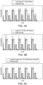
- FIGS. 4A, 4B, and 4C depict overlaying plot of delivered concentration of hydrogen sulfide and the gas sensor output result in measured hydrogen sulfide content.
- the plotted sensor output in Figure 4A is typical of hydrogen sulfide sensor experiencing a phenomenon known as "sleeping", where the sensor response to hydrogen sulfide is initially reduced, but grows stronger with each exposure.
- Figure 4B shows a longer term stabilizing effect of the layered sensor with improved stability and reduced sleep effect.
- Figure 4C it is seen that with the silver co-catalyst at the surface produces a refined response, also with improved stability and reduced sleep effect.
- This Example is directed to disposing a metal chalcogenide at the gas-sensing surface of a surface-doped metal oxide conductor sensing element and its metal oxide semiconductor body.
- Sensing elements were prepared as in Example 1 by doping a tin oxide semiconductor surface with copper deposited by sputtering.
- Sensing element B was prepared as a control with the copper dopant deposited onto the surface of a tin oxide body.
- Sensing element 3 was prepared by depositing silver onto a copper top doped tin oxide body, followed by reaction with hydrogen sulfide to convert the silver to silver sulfide. The sensing elements were exposed to varying concentrations of hydrogen sulfide over time, and the sensor output was recorded in measured hydrogen sulfide content.
- FIGS. 5A and 5B depict overlaying plot of delivered concentration of hydrogen sulfide and the gas sensor output result in measured hydrogen sulfide content.
- the plotted sensor output in Figure 5A is typical of hydrogen sulfide sensor experiencing a phenomenon known as "sleeping", where the sensor response to hydrogen sulfide is initially reduced, but grows stronger with each exposure.
- Figure 5B shows a longer term stabilizing effect of the layered sensor with improved stability reduced sleep effect.
Landscapes
- Chemical & Material Sciences (AREA)
- Chemical Kinetics & Catalysis (AREA)
- Engineering & Computer Science (AREA)
- Materials Engineering (AREA)
- Mechanical Engineering (AREA)
- Metallurgy (AREA)
- Organic Chemistry (AREA)
- Life Sciences & Earth Sciences (AREA)
- Health & Medical Sciences (AREA)
- General Physics & Mathematics (AREA)
- Analytical Chemistry (AREA)
- Biochemistry (AREA)
- General Health & Medical Sciences (AREA)
- Physics & Mathematics (AREA)
- Immunology (AREA)
- Pathology (AREA)
- Electrochemistry (AREA)
- Molecular Biology (AREA)
- Combustion & Propulsion (AREA)
- Food Science & Technology (AREA)
- Medicinal Chemistry (AREA)
- Investigating Or Analyzing Materials By The Use Of Fluid Adsorption Or Reactions (AREA)
Abstract
Description
- Gas sensors have been used in various applications such as process monitoring and control and safety monitoring. As the compounds can also be flammable or explosive, gas detection sensors have also been used for leak detection where such compounds are used or manufactured. Various types of sensors have been used or proposed, including but not limited to metal oxide semiconductor (MOS) sensors, non-dispersive infrared detector (NDIR) sensors, pellistor (pelletized resistor) sensors, high-temperature solid electrolytes that are permeable to oxygen ions, and electrochemical cells.
- The above types of sensors have been used with varying degrees of success in the industrial or laboratory settings where they have been employed. However, many such sensors have limitations that can impact their effectiveness in demanding new and existing applications. For example, pellistor sensors are prone to false alarms due to cross-sensitivity. NDIR sensors have been used in low-volume applications, but can be difficult and expensive to manufacture to commercial tolerances. Electrochemical sensors rely on redox reactions involving tested gas components at electrodes separated by an electrolyte that produce or affect electrical current in a circuit connecting the electrodes. However, solid state electrochemical sensors can be difficult to implement for some materials. For example, solid state electrochemical sensors testing for combustible hydrocarbons may utilize solid electrolytes formed from ceramics such as perovskite, which can require high temperatures (typically in excess of 500°C) that render them impractical for many applications. Some electrochemical sensors that operate at lower temperatures (e.g., carbon monoxide sensors, hydrogen sulfide sensors) require the presence of water at the electrode/electrolyte interface for the electrochemical redox reactions, which can render them impractical for many applications.
- MOS sensors rely on interaction between gas test components such as hydrogen sulfide or hydrocarbons with adsorbed oxygen on the metal oxide semiconductor surface. In the absence of the gas test components, the metal oxide semiconductor adsorbs atmospheric oxygen at the surface, and this adsorbed oxygen captures free electrons from the metal oxide semiconductor material, resulting in a measurable level of base resistance of the semiconductor at a relatively high level. Upon exposure to gas test components such as hydrogen sulfide or hydrocarbon, the gas test component interacts with the adsorbed oxygen, causing it to release free electrons back to the semiconductor material, resulting in a measurable decrease in resistance that can be correlated with a measured level of test gas component.
- In view of the demanding requirements for gas sensors, there remains a need for new alternatives for various environments and applications.
- According to some embodiments of the disclosure, a gas-sensing element comprises a body comprising a semiconductor that is a metal oxide of a first metal. This semiconductor is also referred to herein as a "metal oxide semiconductor" or "MOS". The gas-sensing element includes a gas-sensing surface over the body. The gas-sensing surface comprises metal oxide semiconductor of the first metal and a dopant comprising a second metal that is a transition metal and is different than the first metal. The gas-sensing element also includes an auxiliary component comprising: (1) internally-disposed second metal disposed in the gas-sensing element between the body and the gas-sensing surface, or (2) a metal chalcogenide disposed at the gas-sensing surface or internally disposed in the gas-sensing element between the body and the gas-sensing surface, that stabilizes the second metal at the gas-sensing surface.
- In some embodiments, the auxiliary component comprises: (1) internally-disposed second metal disposed in the gas-sensing element between the body and the gas-sensing surface, and metal oxide semiconductor of the first metal disposed between the internally-disposed second metal and the gas-sensing surface adjacent to the gas-sensing surface.
- In some embodiments where the auxiliary component comprises (1), the gas-sensing element further comprises metal oxide semiconductor of the first metal disposed between the internally-disposed second metal and the gas-sensing surface
- In any one or combination of the foregoing embodiments where the gas-sensing element comprises (1), the gas-sensing element comprises a plurality of alternating deposits of the metal oxide semiconductor of the first metal and deposits of the second metal, disposed in the gas-sensing element between the body and the gas-sensing surface.
- In some embodiments, the auxiliary component comprises: (2) a metal chalcogenide disposed at the gas-sensing surface or internally disposed in the gas-sensing element between the body and the gas-sensing surface adjacent to the gas-sensing surface that stabilizes the second metal at the gas-sensing surface.
- In some embodiments where the auxiliary component comprises (2), the metal chalcogenide is disposed at the gas-sensing surface.
- In some embodiments where the auxiliary component comprises (2), the metal chalcogenide is internally disposed in the gas-sensing element between the body and the gas-sensing surface adjacent to the gas-sensing surface, which stabilizes the second metal at the gas-sensing surface.
- In any one or combination of the foregoing embodiments where the auxiliary component comprises (2), the metal chalcogenide comprises a metal sulfide.
- In any one or combination of the foregoing embodiments, the gas-sensing element comprises a first auxiliary component (1) comprising internally-disposed second metal disposed in the gas-sensing element between the body and the gas-sensing surface, and a second auxiliary component (2) comprising a metal chalcogenide disposed at the gas-sensing surface or internally disposed in the gas-sensing element between the body and the gas-sensing surface adjacent to the gas-sensing surface, that stabilizes the second metal at the gas-sensing surface.
- In any one or combination of the foregoing embodiments, the second metal comprises one or more group 5 to
group 11 transition metals. - In any one or combination of the foregoing embodiments, the first metal comprises any one of the commonly used metals for metal oxide semiconductors, including aluminum, bismuth, cadmium, cerium, chromium, cobalt, copper, iron, gallium, indium, molybdenum, niobium, tantalum, tin, titanium, tungsten, vanadium or zinc.
- In any one or combination of the foregoing embodiments, the first metal comprises tin and the second metal comprises copper.
- In some embodiments, a gas sensor comprises the gas-sensing element of any one or combination of the foregoing embodiments disposed between electrodes connected by a voltage-measuring circuit, current-measuring circuit, resistance-measuring circuit, impedance-measuring circuit, or conductance-measuring circuit.
- In some embodiments, the resistance-measuring circuit of the gas sensor comprises a signal processor calibrated to determine hydrogen sulfide concentration based on measured resistance at the gas-sensing surface.
- In some embodiments, a method of using the gas sensor of any one or combination of the foregoing embodiments comprises exposing the gas-sensing surface to a gas to be tested, and measuring resistance of the gas-sensing element between the electrodes to determine a presence or concentration of a gas component.
- In any one or combination of the foregoing embodiments, the gas sensor tests for or is configured to test for hydrogen sulfide.
- In some embodiments, a method of making a gas-sensing element comprises disposing a transition metal dopant comprising a second metal at a surface of a semiconductor that is a metal oxide of a first metal, and: (1) disposing second metal in the gas-sensing element between the surface and a body of the metal oxide semiconductor of the first metal, or (2) disposing a metal chalcogenide at the surface or in the gas-sensing element between a body comprising the metal oxide semiconductor of the first metal and the doped surface and adjacent to the doped surface.
- In some embodiments where the method of making a gas-sensing element comprises (1), the method comprises depositing second metal over the body, depositing metal oxide semiconductor of the first metal over the deposited second metal, and depositing second metal over the deposited metal oxide semiconductor of the first metal.
- In any one or combination of embodiments where the method of making a gas-sensing element comprises (1), the method comprises alternately depositing second metal and metal oxide semiconductor of the first metal to form a plurality of alternating deposits of second metal and metal oxide semiconductor of the first metal between the body and the doped surface.
- In any one or combination of embodiments where the method of making a gas-sensing element comprises (2), the method comprises disposing the metal chalcogenide on top of the doped surface.
- In any one or combination of embodiments where the method of making a gas-sensing element comprises (2), the method comprises disposing the metal chalcogenide between the body of metal oxide semiconductor of the first metal and the doped surface adjacent to the doped surface.
- Subject matter of this disclosure is particularly pointed out and distinctly claimed in the claims at the conclusion of the specification. The foregoing and other features, and advantages of the present disclosure are apparent from the following detailed description taken in conjunction with the accompanying drawings in which:
-
FIG. 1 is a schematic depiction of a cross-section view of an example embodiment of a gas-sensing element; -
FIG. 2 is a schematic depiction of a cross-section view of another example embodiment of a gas-sensing element; -
FIG. 3 is a schematic depiction of a gas sensor; -
FIGS. 4A, 4B, and 4B are plots of gas sensor outputs of tested sensing elements; and -
FIGS. 5A and 5B are plots of gas sensor outputs of tested sensing elements. - With reference now to the Figures,
FIGS. 1 and 2 schematically depict an cross-section view of an example embodiment of a gas-sensing element. As shown inFIG. 1 , gas-sensing element 10, 10' includes a metaloxide semiconductor body 12 disposed on a substrate having a gas-sensing surface 14 that comprises the metal oxide semiconductor material and a transition metal dopant. Typically, the gas-sensing elements 10, 10' are disposed on asubstrate 11 as illustrated inFIGS. 1 and 2 . Examples of metal oxide semiconductors include but are not limited to aluminum (III) oxide, bismuth (III) oxide, cadmium oxide, cerium (IV) oxide, chromium (III) oxide, cobalt (III) oxide, copper (II) oxide, iron (III) oxide, gallium (III) oxide, Indium (III) oxide, molybdenum (VI) oxide, niobium (V) oxide, nickel (II) oxide, tantalum (V) oxide, tin (IV) oxide, titanium (IV) oxide, tungsten (VI) oxide, vanadium (5) oxide, zinc (II) oxide and mixtures of these. Mixed metal oxides (e.g., SnO2-CuO or other mixed oxides of the above metal oxides) can also be utilized, and the term "first metal" as used herein includes metal mixtures. Transition metal dopants are used to enhance the responsiveness of the metal oxide semiconductor to target gases being sensed for, such as hydrogen sulfide, and to allow for the target gas to be distinguished from other gases that may also produce a change in electrical resistance at the gas-sensing surface 14. In some embodiments, the dopant is a group 5 togroup 11 transition metal. Examples of transition metal dopants include copper, silver, gold, iron, ruthenium, nickel, platinum, palladium, or vanadium. Although any of the above materials can exhibit a change in electrical resistance in response to exposure to various test gas components, the use of some materials for particular applications has been more widespread than other materials. For example, copper-doped tin oxide can be used for hydrogen sulfide sensing elements and platinum and palladium doping is commonly used in sensing for hydrogen or hydrocarbons. Such combinations and others are included within this disclosure. Various other materials can be included in the metal oxide semiconductor at the gas-sensingsurface 14, including but not limited to noble metals (e.g., silver, gold). Dopants, metal oxide semiconductors, other materials, and combinations thereof are disclosed in Kaur, M. Aswal, D.K. and Yakhmi, J.V." Chemiresistor Gas Sensors: Materials, Mechanisms and Fabrication" Chapter 2 in , Science and Technology of Chemiresistor Gas Sensors, Ed. Aswal, D.K. and Gupta, S.K. Nova Science Publishers, New York, 2007., and in Bochenkov, V.E. and Sergeev, G.B. "Sensitivity, Selectivity, and Stability of Gas-Sensitive Metal-Oxide Nanostructures" Chapter 2, inMetal Oxide Nanostructures and Their Applications. , American Scientific Publishers, California, 2010 the disclosures of each of which is incorporated herein by reference in its entirety. - As mentioned above, the gas-sensing element includes an auxiliary component comprising: (1) internally-disposed second metal disposed in the gas-sensing element between the body and the gas-sensing surface, or (2) a metal chalcogenide disposed at the gas-sensing surface or internally disposed in the gas-sensing element between the body and the gas-sensing surface adjacent to the gas-sensing surface that stabilizes the second metal at the gas-sensing surface. An example embodiment of internally-disposed
second metal 16 between the metaloxide semiconductor body 12 and the gas-sensing surface is schematically depicted inFIG. 1 . In some embodiments, the element also includesmetal oxide semiconductor 18 that is free of second metal (e.g., high purity metal oxide semiconductor) disposed between the internally disposedsecond metal 16 and the second metal-doped gas-sensingsurface 14. In some embodiments, the sensing element can optionally include a plurality of deposits of second metal alternating with deposits of metal oxide semiconductor, as illustrated inFIG. 1 with additionalsecond metal 20 and additionalmetal oxide semiconductor 22. Four deposits are illustrated inFIG. 1 , but larger numbers (e.g., more than 10) of such alternating deposits can also be used. - Deposition of second metal or metal oxide semiconductor onto the metal oxide semiconductor body can be performed using thermal deposition techniques such as sputtering, physical vapor deposition, chemical vapor deposition, or thermal spray. Alternatively, any or all of the deposits can be grown layer by layer, for example, using solution-based epitaxy techniques such as sol-gel processing to form the individual layers. The term "layer" as used herein means any deposit of material, including islands and partial layers, as well as contiguous layers of material. Layers of internally-disposed second metal can range in thickness from 0 (meaning no contiguous layer such as where areas (e.g., islands) of deposited second metal having thicknesses as low as the mass equivalent of 0.2 Angstroms) to 20 nm. Layers of internally-disposed metal oxide semiconductor, which can be interspersed with deposits of the second metal, can range in thickness from 1 to 60 nm.
- As mentioned above, the gas-sensing element includes an auxiliary component comprising: (1) internally-disposed second metal disposed in the gas-sensing element between the body and the gas-sensing surface, or (2) a metal chalcogenide disposed at the gas-sensing surface or internally disposed in the gas-sensing element between the body and the gas-sensing surface adjacent to the gas-sensing surface that stabilizes the second metal at the gas-sensing surface. An example embodiment of a metal chalcogenide disposed at the gas-sensing surface or internally disposed in the gas-sensing element between the body and the gas-sensing surface adjacent to the gas-sensing surface is schematically depicted in
FIG. 2 . As shown inFIG. 2 , gas-sensing element 10' includes metaloxide semiconductor body 12 and doped metal oxide semiconductor gas-sensingsurface 14. In some embodiments, the metal chalcogenide can be applied internal to the gas-sensing element adjacent to the gas-sensingsurface 14, as depicted bymetal chalcogenide 24 inFIG. 2 . In some embodiments, the metal chalcogenide can be applied over the gas-sensing surface, as depicted bymetal chalcogenide 26 inFIG. 2 . In some embodiments, the metal chalcogenide can be disposed (not shown) in the gas-sensingsurface 14. In some embodiments, the metal chalcogenide can be disposed in a combination of more than one of the specified locations (e.g., both over and under the gas-sensingsurface 14, or mixed in with and underneath the gas-sensing surface 14). In some embodiments (not shown), the auxiliary component can include both (1) internally-disposed second metal disposed in the gas-sensing element between the body and the gas-sensing surface, and (2) a metal chalcogenide disposed at the gas-sensing surface or internally disposed in the gas-sensing element between the body and the gas-sensing surface adjacent to the gas-sensing surface that stabilizes the second metal at the gas-sensing surface. For example, a gas-sensing element could have a metal chalcogenide over (24) or in the gas-sensingsurface 14 and second metal disposed 16, 20 between the gas-sensingsurface 14 and the metaloxide semiconductor body 12. In another example, a gas-sensing element could have ametal chalcogenide 22 internally disposed adjacent to the gas-sensingsurface 14, a metaloxide semiconductor layer 18 under themetal chalcogenide 22, andsecond metal 16 under the metaloxide semiconductor layer 18. - Examples of chalcogens for the metal chalcogenide include sulfur, selenium and tellurium. In some embodiments, the chalcogen is a chalcogen having a higher number on the periodic table than oxygen. Metals for the metal chalcogenide include but are not limited to silver, lead, zinc, iron, cadmium or other metals that provide a stable chalcogenide at the operating temperature of the sensing element. In some embodiments, the metal chalcogenide comprises a metal sulfide. Examples of metal sulfides include but are not limited to silver sulfide, lead sulfide, zinc sulfide, iron sulfide or cadmium sulfide. In some embodiments, the metal chalcogenide comprises silver sulfide. The metal chalcogenide can be introduced by applying the metal (e.g., silver, lead, zinc, iron) below or above the gas-sensing
surface 14 using sputtering or any of the techniques referenced above for application ofsecond metal 16 ormetal oxide semiconductor 18, reacting with a reactive chalcogenide such as hydrogen sulfide, and sintering. Sintering may promote spreading of the metal chalcogenide through the gas-sensingsurface 14. - The above-described sensing element can be incorporated into a
sensor 30 as schematically depicted inFIG. 3 . As shown inFIG. 3 ,gas sensor 30 comprises the gas-sensingelement 10 with metaloxide semiconductor body 12 and gas-sensingsurface 14, integrated with either parallel or interdigitated (as shown, for higher gain)electrodes surface 14 disposed between theinterdigitated electrodes electrodes sensing element 10, but can also be disposed at the bottom. The electrodes are connected externally to the gas-sensingelement 10 by anelectrical circuit 36 that includes asignal processor 38.Signal processor 38 can be a voltmeter or ampere meter, but in many cases comprises a potentiostatic circuit, voltage divider circuit, bridge circuit, microprocessor, electronic control unit (ECU), or similar electronic device with integrated voltage and or amperage measurement functions and also can apply a voltage bias between theelectrodes FIG. 3 , but can be incorporated into the sensor by the skilled person. - Additional disclosure is provided in the following Examples:
- As demonstrated by the following non-limiting example embodiments, some embodiments can provide a technical effect that can promotes gas sensor stability and can mitigate gas sensor drift.
- This Example is directed to disposing second metal between the gas-sensing surface of a sensing element and its metal oxide semiconductor body. Sensing elements were prepared by doping a tin oxide semiconductor surface with copper deposited by physical deposition means. Sensing element A was prepared as a control with the copper and gold dopants deposited onto the surface of a tin oxide body. Sensing element 1 was prepared by depositing copper and tin oxide in alternating layers to a tin oxide body, finishing with copper. Sensing element 2 was prepared similar to sensing element 1, except that silver was deposited and sulfided after the top copper dopant application. All three sensors were sintered. The sensing elements were exposed to varying concentrations of hydrogen sulfide over time, and the sensor output was recorded in measured hydrogen sulfide content. The results are shown in
FIGS. 4A (sensing element A), 4B (sensing element 1), and 4C (sensing element 2).FIGS. 4A, 4B, and 4C depict overlaying plot of delivered concentration of hydrogen sulfide and the gas sensor output result in measured hydrogen sulfide content. The plotted sensor output inFigure 4A is typical of hydrogen sulfide sensor experiencing a phenomenon known as "sleeping", where the sensor response to hydrogen sulfide is initially reduced, but grows stronger with each exposure. In contrast,Figure 4B shows a longer term stabilizing effect of the layered sensor with improved stability and reduced sleep effect. InFigure 4C , it is seen that with the silver co-catalyst at the surface produces a refined response, also with improved stability and reduced sleep effect. - This Example is directed to disposing a metal chalcogenide at the gas-sensing surface of a surface-doped metal oxide conductor sensing element and its metal oxide semiconductor body. Sensing elements were prepared as in Example 1 by doping a tin oxide semiconductor surface with copper deposited by sputtering. Sensing element B was prepared as a control with the copper dopant deposited onto the surface of a tin oxide body. Sensing element 3 was prepared by depositing silver onto a copper top doped tin oxide body, followed by reaction with hydrogen sulfide to convert the silver to silver sulfide. The sensing elements were exposed to varying concentrations of hydrogen sulfide over time, and the sensor output was recorded in measured hydrogen sulfide content. The results are shown in
FIGS. 5A (sensing element A) and 5B (sensing element 3).FIGS. 5A and 5B depict overlaying plot of delivered concentration of hydrogen sulfide and the gas sensor output result in measured hydrogen sulfide content. The plotted sensor output inFigure 5A is typical of hydrogen sulfide sensor experiencing a phenomenon known as "sleeping", where the sensor response to hydrogen sulfide is initially reduced, but grows stronger with each exposure. In contrast,Figure 5B shows a longer term stabilizing effect of the layered sensor with improved stability reduced sleep effect. - While the present disclosure has been described in detail in connection with only a limited number of embodiments, it should be readily understood that the present disclosure is not limited to such disclosed embodiments. Rather, the present disclosure can be modified to incorporate any number of variations, alterations, substitutions or equivalent arrangements not heretofore described, but which are commensurate with the spirit and scope of the present disclosure. Additionally, while various embodiments of the present disclosure have been described, it is to be understood that aspects of the present disclosure may include only some of the described embodiments. Accordingly, the present disclosure is not to be seen as limited by the foregoing description, but is only limited by the scope of the appended claims.
-
- 1. A gas-sensing element, comprising:
- a body comprising a semiconductor that is a metal oxide of a first metal;
- a gas-sensing surface over the body, comprising metal oxide semiconductor of the first metal and a dopant comprising a second metal that is a transition metal and is different than the first metal; and
- an auxiliary component comprising:
- (1) internally-disposed second metal disposed in the gas-sensing element between the body and the gas-sensing surface, or
- (2) a metal chalcogenide disposed at the gas-sensing surface or internally disposed in the gas-sensing element between the body and the gas-sensing surface adjacent to the gas-sensing surface.
- 2. The gas-sensing element of embodiment 1, wherein the auxiliary component comprises: (1) internally-disposed second metal disposed in the gas-sensing element between the body and the gas-sensing surface, and metal oxide semiconductor of the first metal disposed between the internally-disposed second metal and the gas-sensing surface adjacent to the gas-sensing surface.
- 3. The gas-sensing element of embodiment 2, wherein, further comprising metal oxide semiconductor of the first metal disposed between the internally-disposed second metal and the gas-sensing surface.
- 4. The gas-sensing element of embodiments 2 or 3, comprising a plurality of alternating deposits of the metal oxide semiconductor of the first metal and deposits of the second metal, disposed in the gas-sensing element between the body and the gas-sensing surface.
- 5. The gas-sensing element of any of embodiments 1-4, wherein the auxiliary component comprises: (2) a metal chalcogenide disposed at the gas-sensing surface or internally disposed in the gas-sensing element between the body and the gas-sensing surface adjacent to the gas-sensing surface, that stabilizes the second metal at the gas-sensing surface.
- 6. The gas-sensing element of embodiment 5, wherein the metal chalcogenide is disposed at the gas-sensing surface.
- 7. The gas-sensing element of embodiment 5, wherein the metal chalcogenide is internally disposed in the gas-sensing element between the body and the gas-sensing surface adjacent to the gas-sensing surface, which stabilizes the second metal at the gas-sensing surface.
- 8. The gas-sensing element of any of embodiments 5-7, wherein the metal chalcogenide comprises a metal sulfide.
- 9. The gas-sensing element of any of embodiments 1-8, wherein the second metal comprises one or more group 5 to
group 11 transition metals. - 10. The gas-sensing element of any of embodiments 1-9, wherein the first metal comprises aluminum, bismuth, cadmium, cerium, chromium, cobalt, copper, iron, gallium, indium, molybdenum, niobium, tantalum, tin, titanium, tungsten, vanadium or zinc.
- 11. The gas-sensing element of any of embodiments 1-10, wherein the first metal comprises tin and the second metal comprises copper.
- 12. A gas sensor comprising the gas-sensing element of any of embodiments 1-11 disposed between electrodes connected by a voltage-measuring circuit, current-measuring circuit, resistance-measuring circuit, impedance-measuring circuit, or conductance-measuring circuit.
- 13. The gas sensor of embodiment12, wherein the resistance-measuring circuit comprises a signal processor calibrated to determine hydrogen sulfide concentration based on measured resistance at the gas-sensing surface.
- 14. A method of using the gas sensor of
embodiments - 15. The method of embodiment14, wherein the gas component comprises hydrogen sulfide.
- 16. A method of making a gas-sensing element, comprising disposing a transition metal dopant comprising a second metal that is a transition metal at a surface of a semiconductor that is a metal oxide of a first metal, and: (1) disposing second metal in the gas-sensing element between the surface and a body of the metal oxide semiconductor of the first metal, or (2) disposing a metal chalcogenide on top of the doped surface or in the gas-sensing element between a body comprising the metal oxide semiconductor of the first metal and the doped surface adjacent to the doped surface.
- 17. The method of embodiment16, wherein (1) comprises depositing second metal over the body, depositing metal oxide semiconductor of the first metal over the deposited second metal, and depositing second metal over the deposited metal oxide semiconductor of the first metal.
- 18. The method of
embodiments 16 or 17, wherein (1) comprises alternately depositing second metal and metal oxide semiconductor of the first metal to form a plurality of alternating deposits of second metal and metal oxide semiconductor of the first metal between the body and the doped surface. - 19. The method of any of embodiments16-18, wherein (2) comprises disposing the metal chalcogenide on top of the doped surface.
- 20. The method of any of embodiments16-19, wherein (2) comprises disposing the metal chalcogenide between the body of metal oxide semiconductor of the first metal and the doped surface adjacent to the doped surface.
Claims (15)
- A gas-sensing element, comprising:a body comprising a semiconductor that is a metal oxide of a first metal;a gas-sensing surface over the body, comprising metal oxide semiconductor of the first metal and a dopant comprising a second metal that is a transition metal and is different than the first metal; andan auxiliary component comprising:
a metal chalcogenide internally disposed in the gas-sensing element between the body and the gas-sensing surface adjacent to the gas-sensing surface or disposed at the gas-sensing surface. - The gas-sensing element of claim 1, wherein, further comprising metal oxide semiconductor of the first metal disposed between the internally-disposed second metal and the gas-sensing surface.
- The gas-sensing element of claims 1 or 2, comprising a plurality of alternating deposits of the metal oxide semiconductor of the first metal and deposits of the second metal, disposed in the gas-sensing element between the body and the gas-sensing surface.
- The gas-sensing element of any of claims 1-3, wherein the auxiliary component stabilizes the second metal at the gas-sensing surface.
- The gas-sensing element of claim 4, wherein the metal chalcogenide is disposed at the gas-sensing surface.
- The gas-sensing element of claim 4, wherein the metal chalcogenide is internally disposed in the gas-sensing element between the body and the gas-sensing surface adjacent to the gas-sensing surface, which stabilizes the second metal at the gas-sensing surface.
- The gas-sensing element of any of claims 4-6, wherein the metal chalcogenide comprises a metal sulfide.
- The gas-sensing element of any of claims 1-7, wherein the second metal comprises one or more group 5 to group 11 transition metals.
- The gas-sensing element of any of claims 1-8, wherein the first metal comprises aluminum, bismuth, cadmium, cerium, chromium, cobalt, copper, iron, gallium, indium, molybdenum, niobium, tantalum, tin, titanium, tungsten, vanadium or zinc.
- The gas-sensing element of any of claims 1-9, wherein the first metal comprises tin and the second metal comprises copper.
- A gas sensor comprising the gas-sensing element of any of claims 1-10 disposed between electrodes connected by a voltage-measuring circuit, current-measuring circuit, resistance-measuring circuit, impedance-measuring circuit, or conductance-measuring circuit , preferably wherein the resistance-measuring circuit comprises a signal processor calibrated to determine hydrogen sulfide concentration based on measured resistance at the gas-sensing surface.
- A method of using the gas sensor of claims 10 or 11, comprising exposing the gas-sensing surface to a gas to be tested, and measuring resistance of the gas-sensing element between the electrodes to determine a presence or concentration of a gas component, , preferably wherein the gas component comprises hydrogen sulfide.
- A method of making a gas-sensing element, comprising disposing a transition metal dopant comprising a second metal that is a transition metal at a surface of a semiconductor that is a metal oxide of a first metal, and disposing a metal chalcogenide in the gas-sensing element between a body comprising the metal oxide semiconductor of the first metal and the doped surface adjacent to the doped surface or on top of the doped surface.
- The method of claim 13, wherein disposing the metal chalcogenide comprises disposing the metal chalcogenide on top of the doped surface.
- The method of any of claims 13-14, wherein disposing the a metal chalcogenide comprises disposing the metal chalcogenide between the body of metal oxide semiconductor of the first metal and the doped surface adjacent to the doped surface.
Applications Claiming Priority (3)
| Application Number | Priority Date | Filing Date | Title |
|---|---|---|---|
| US201662409626P | 2016-10-18 | 2016-10-18 | |
| PCT/US2017/057181 WO2018075634A1 (en) | 2016-10-18 | 2017-10-18 | Gas sensor |
| EP17791891.9A EP3529601B1 (en) | 2016-10-18 | 2017-10-18 | Gas sensing element |
Related Parent Applications (2)
| Application Number | Title | Priority Date | Filing Date |
|---|---|---|---|
| EP17791891.9A Division-Into EP3529601B1 (en) | 2016-10-18 | 2017-10-18 | Gas sensing element |
| EP17791891.9A Division EP3529601B1 (en) | 2016-10-18 | 2017-10-18 | Gas sensing element |
Publications (2)
| Publication Number | Publication Date |
|---|---|
| EP4166940A1 true EP4166940A1 (en) | 2023-04-19 |
| EP4166940B1 EP4166940B1 (en) | 2025-04-16 |
Family
ID=60191567
Family Applications (2)
| Application Number | Title | Priority Date | Filing Date |
|---|---|---|---|
| EP17791891.9A Active EP3529601B1 (en) | 2016-10-18 | 2017-10-18 | Gas sensing element |
| EP22202241.0A Active EP4166940B1 (en) | 2016-10-18 | 2017-10-18 | Gas sensor, method of making the sensor and method of using the sensor |
Family Applications Before (1)
| Application Number | Title | Priority Date | Filing Date |
|---|---|---|---|
| EP17791891.9A Active EP3529601B1 (en) | 2016-10-18 | 2017-10-18 | Gas sensing element |
Country Status (7)
| Country | Link |
|---|---|
| US (1) | US20190317036A1 (en) |
| EP (2) | EP3529601B1 (en) |
| BR (1) | BR112019007608A2 (en) |
| CA (1) | CA3040910A1 (en) |
| MX (1) | MX2019004380A (en) |
| RU (1) | RU2019110761A (en) |
| WO (1) | WO2018075634A1 (en) |
Families Citing this family (4)
| Publication number | Priority date | Publication date | Assignee | Title |
|---|---|---|---|---|
| DE102017208418A1 (en) * | 2017-05-18 | 2018-11-22 | Robert Bosch Gmbh | Method for producing a nanocrystalline, gas-sensitive layer structure, corresponding nanocrystalline, gas-sensitive layer structure, and gas sensor with a corresponding nanocrystalline, gas-sensitive layer structure |
| TWI832211B (en) * | 2022-04-15 | 2024-02-11 | 崑山科技大學 | Method for preparing hydrogen sensor by sputtering process |
| US20230358715A1 (en) | 2022-05-06 | 2023-11-09 | Carrier Corporation | Surface modified matrix barrier for a gas detector device |
| US20250102456A1 (en) * | 2023-08-04 | 2025-03-27 | Carrier Corporation | Gas-sensing elements and a method of manufacturing thereof |
Citations (3)
| Publication number | Priority date | Publication date | Assignee | Title |
|---|---|---|---|---|
| US5624640A (en) * | 1993-10-12 | 1997-04-29 | Robert Bosch Gmbh | Sensor for detecting nitrogen oxide |
| JP2007024508A (en) * | 2005-07-12 | 2007-02-01 | Fuji Electric Fa Components & Systems Co Ltd | Thin film gas sensor |
| EP1950558A1 (en) * | 2007-01-16 | 2008-07-30 | Ngk Spark Plug Co., Ltd. | Gas sensor |
Family Cites Families (3)
| Publication number | Priority date | Publication date | Assignee | Title |
|---|---|---|---|---|
| DE4445359A1 (en) * | 1994-12-20 | 1996-06-27 | Bosch Gmbh Robert | Sensor for the detection of flammable gases |
| US9831427B1 (en) * | 2014-08-21 | 2017-11-28 | National Technology & Engineering Solutions Of Sandia, Llc | Ion-barrier for memristors/ReRAM and methods thereof |
| KR101767886B1 (en) * | 2015-07-31 | 2017-08-14 | 한양대학교 에리카산학협력단 | Multi-layer ceramic/metal type gas sensor and manufacturing method of the same |
-
2017
- 2017-10-18 US US16/343,156 patent/US20190317036A1/en not_active Abandoned
- 2017-10-18 MX MX2019004380A patent/MX2019004380A/en unknown
- 2017-10-18 EP EP17791891.9A patent/EP3529601B1/en active Active
- 2017-10-18 BR BR112019007608A patent/BR112019007608A2/en not_active Application Discontinuation
- 2017-10-18 WO PCT/US2017/057181 patent/WO2018075634A1/en not_active Ceased
- 2017-10-18 EP EP22202241.0A patent/EP4166940B1/en active Active
- 2017-10-18 RU RU2019110761A patent/RU2019110761A/en not_active Application Discontinuation
- 2017-10-18 CA CA3040910A patent/CA3040910A1/en not_active Abandoned
Patent Citations (3)
| Publication number | Priority date | Publication date | Assignee | Title |
|---|---|---|---|---|
| US5624640A (en) * | 1993-10-12 | 1997-04-29 | Robert Bosch Gmbh | Sensor for detecting nitrogen oxide |
| JP2007024508A (en) * | 2005-07-12 | 2007-02-01 | Fuji Electric Fa Components & Systems Co Ltd | Thin film gas sensor |
| EP1950558A1 (en) * | 2007-01-16 | 2008-07-30 | Ngk Spark Plug Co., Ltd. | Gas sensor |
Non-Patent Citations (6)
| Title |
|---|
| BOCHENKOV, V.E.SERGEEV, G.B.: "Metal Oxide Nanostructures and Their Applications", 2010, AMERICAN SCIENTIFIC PUBLISHERS, article "Sensitivity, Selectivity, and Stability of Gas-Sensitive Metal-Oxide Nanostructures" |
| GONG J ET AL: "Micromachined nanocrystalline silver doped SnO"2 H"2S sensor", SENSORS AND ACTUATORS B: CHEMICAL, ELSEVIER BV, NL, vol. 114, no. 1, 30 March 2006 (2006-03-30), pages 32 - 39, XP027971379, ISSN: 0925-4005, [retrieved on 20060330] * |
| KAUR, M.ASWAL, D.K.YAKHMI, J.V.: "Science and Technology of Chemiresistor Gas Sensors", 2007, SCIENCE PUBLISHERS, article "Chemiresistor Gas Sensors: Materials, Mechanisms and Fabrication" |
| NIRANJAN R S ET AL: "A novel hydrogen sulfide room temperature sensor based on copper nanocluster functionalized tin oxide thin films", SENSORS AND ACTUATORS B: CHEMICAL: INTERNATIONAL JOURNAL DEVOTED TO RESEARCH AND DEVELOPMENT OF PHYSICAL AND CHEMICAL TRANSDU, ELSEVIER BV, NL, vol. 85, no. 1-2, 20 June 2002 (2002-06-20), pages 26 - 32, XP004358217, ISSN: 0925-4005, DOI: 10.1016/S0925-4005(02)00046-1 * |
| R.S. NIRANJAN ET AL: "High H2S-sensitive copper-doped tin oxide thin film", MATERIALS CHEMISTRY AND PHYSICS, vol. 80, no. 1, 14 November 2002 (2002-11-14), Switzerland, Taiwan, Republic of China, pages 250 - 256, XP055437751, ISSN: 0254-0584, DOI: 10.1016/S0254-0584(02)00467-4 * |
| YUANDA W ET AL: "Thin film sensors of SnO"2-CuO-SnO"2 sandwich structure to H"2S", SENSORS AND ACTUATORS B: CHEMICAL, ELSEVIER BV, NL, vol. 79, no. 2-3, 15 October 2001 (2001-10-15), pages 187 - 191, XP004305519, ISSN: 0925-4005, DOI: 10.1016/S0925-4005(01)00873-5 * |
Also Published As
| Publication number | Publication date |
|---|---|
| EP3529601B1 (en) | 2023-01-04 |
| EP3529601A1 (en) | 2019-08-28 |
| US20190317036A1 (en) | 2019-10-17 |
| CA3040910A1 (en) | 2018-04-26 |
| WO2018075634A1 (en) | 2018-04-26 |
| BR112019007608A2 (en) | 2019-07-02 |
| MX2019004380A (en) | 2019-08-12 |
| RU2019110761A (en) | 2020-11-20 |
| EP4166940B1 (en) | 2025-04-16 |
Similar Documents
| Publication | Publication Date | Title |
|---|---|---|
| Mandayo et al. | Strategies to enhance the carbon monoxide sensitivity of tin oxide thin films | |
| Sen et al. | Highly sensitive hydrogen sulphide sensors operable at room temperature | |
| Kapse et al. | Nanocrystalline Ni0. 6Zn0. 4Fe2O4: a novel semiconducting material for ethanol detection | |
| EP4166940B1 (en) | Gas sensor, method of making the sensor and method of using the sensor | |
| Schierbaum et al. | Specific palladium and platinum doping for SnO2-based thin film sensor arrays | |
| US20100032292A1 (en) | Ammonia gas sensor | |
| Balouria et al. | Temperature dependent H2S and Cl2 sensing selectivity of Cr2O3 thin films | |
| Murthy et al. | Application of principal component analysis to gas sensing characteristics of Cr0. 8Fe0. 2NbO4 thick film array | |
| Desai et al. | Indium sesquitelluride (In2Te3) thin film gas sensor for detection of carbon dioxide | |
| EP2071324A1 (en) | Hydrogen sensor | |
| Cantalini et al. | Investigation on the cross sensitivity of NO2 sensors based on In2O3 thin films prepared by sol-gel and vacuum thermal evaporation | |
| Pugh et al. | Enhanced gas sensing performance of indium doped zinc oxide nanopowders | |
| JP3845741B2 (en) | Nitrogen oxide detection method and sensor element for nitrogen oxide detection | |
| Niskanen et al. | Atomic layer deposition of tin dioxide sensing film in microhotplate gas sensors | |
| US6513364B1 (en) | Hydrogen sensor | |
| Haidry et al. | Sensing mechanism of low temperature NO2 sensing with top–bottom electrode (TBE) geometry | |
| WO1997042495A1 (en) | Solid state electrochemical cell for measuring components of a gas mixture, and related measurement method | |
| Malavasi et al. | Materials development for CO-detection with improved selectivity through catalytic activation | |
| Yude et al. | The n+ n combined structure gas sensor based on burnable gases | |
| RU91763U1 (en) | DIFFERENTIAL GAS SENSOR | |
| RU2403563C1 (en) | Differential sensor for gas analyser | |
| RU2546849C2 (en) | Semiconductor oxygen sensor | |
| KR101133820B1 (en) | Electrochemical sensor | |
| RU2677093C1 (en) | Method of manufacturing a chemoresistor based on cobalt oxide nanostructures by electrochemical method | |
| JPH02662B2 (en) |
Legal Events
| Date | Code | Title | Description |
|---|---|---|---|
| PUAI | Public reference made under article 153(3) epc to a published international application that has entered the european phase |
Free format text: ORIGINAL CODE: 0009012 |
|
| STAA | Information on the status of an ep patent application or granted ep patent |
Free format text: STATUS: THE APPLICATION HAS BEEN PUBLISHED |
|
| AC | Divisional application: reference to earlier application |
Ref document number: 3529601 Country of ref document: EP Kind code of ref document: P |
|
| AK | Designated contracting states |
Kind code of ref document: A1 Designated state(s): AL AT BE BG CH CY CZ DE DK EE ES FI FR GB GR HR HU IE IS IT LI LT LU LV MC MK MT NL NO PL PT RO RS SE SI SK SM TR |
|
| P01 | Opt-out of the competence of the unified patent court (upc) registered |
Effective date: 20230527 |
|
| STAA | Information on the status of an ep patent application or granted ep patent |
Free format text: STATUS: REQUEST FOR EXAMINATION WAS MADE |
|
| 17P | Request for examination filed |
Effective date: 20231012 |
|
| RBV | Designated contracting states (corrected) |
Designated state(s): AL AT BE BG CH CY CZ DE DK EE ES FI FR GB GR HR HU IE IS IT LI LT LU LV MC MK MT NL NO PL PT RO RS SE SI SK SM TR |
|
| RAP3 | Party data changed (applicant data changed or rights of an application transferred) |
Owner name: CARRIER CORPORATION |
|
| GRAP | Despatch of communication of intention to grant a patent |
Free format text: ORIGINAL CODE: EPIDOSNIGR1 |
|
| STAA | Information on the status of an ep patent application or granted ep patent |
Free format text: STATUS: GRANT OF PATENT IS INTENDED |
|
| INTG | Intention to grant announced |
Effective date: 20250204 |
|
| GRAS | Grant fee paid |
Free format text: ORIGINAL CODE: EPIDOSNIGR3 |
|
| GRAA | (expected) grant |
Free format text: ORIGINAL CODE: 0009210 |
|
| STAA | Information on the status of an ep patent application or granted ep patent |
Free format text: STATUS: THE PATENT HAS BEEN GRANTED |
|
| AC | Divisional application: reference to earlier application |
Ref document number: 3529601 Country of ref document: EP Kind code of ref document: P |
|
| AK | Designated contracting states |
Kind code of ref document: B1 Designated state(s): AL AT BE BG CH CY CZ DE DK EE ES FI FR GB GR HR HU IE IS IT LI LT LU LV MC MK MT NL NO PL PT RO RS SE SI SK SM TR |
|
| REG | Reference to a national code |
Ref country code: GB Ref legal event code: FG4D |
|
| REG | Reference to a national code |
Ref country code: CH Ref legal event code: EP |
|
| REG | Reference to a national code |
Ref country code: IE Ref legal event code: FG4D |
|
| REG | Reference to a national code |
Ref country code: DE Ref legal event code: R096 Ref document number: 602017089016 Country of ref document: DE |
|
| PG25 | Lapsed in a contracting state [announced via postgrant information from national office to epo] |
Ref country code: NL Free format text: LAPSE BECAUSE OF FAILURE TO SUBMIT A TRANSLATION OF THE DESCRIPTION OR TO PAY THE FEE WITHIN THE PRESCRIBED TIME-LIMIT Effective date: 20250416 |
|
| REG | Reference to a national code |
Ref country code: AT Ref legal event code: MK05 Ref document number: 1786017 Country of ref document: AT Kind code of ref document: T Effective date: 20250416 |
|
| PG25 | Lapsed in a contracting state [announced via postgrant information from national office to epo] |
Ref country code: FI Free format text: LAPSE BECAUSE OF FAILURE TO SUBMIT A TRANSLATION OF THE DESCRIPTION OR TO PAY THE FEE WITHIN THE PRESCRIBED TIME-LIMIT Effective date: 20250416 Ref country code: ES Free format text: LAPSE BECAUSE OF FAILURE TO SUBMIT A TRANSLATION OF THE DESCRIPTION OR TO PAY THE FEE WITHIN THE PRESCRIBED TIME-LIMIT Effective date: 20250416 Ref country code: PT Free format text: LAPSE BECAUSE OF FAILURE TO SUBMIT A TRANSLATION OF THE DESCRIPTION OR TO PAY THE FEE WITHIN THE PRESCRIBED TIME-LIMIT Effective date: 20250818 |
|
| REG | Reference to a national code |
Ref country code: LT Ref legal event code: MG9D |
|
| PG25 | Lapsed in a contracting state [announced via postgrant information from national office to epo] |
Ref country code: GR Free format text: LAPSE BECAUSE OF FAILURE TO SUBMIT A TRANSLATION OF THE DESCRIPTION OR TO PAY THE FEE WITHIN THE PRESCRIBED TIME-LIMIT Effective date: 20250717 |
|
| PGFP | Annual fee paid to national office [announced via postgrant information from national office to epo] |
Ref country code: NO Payment date: 20250925 Year of fee payment: 9 |
|
| PG25 | Lapsed in a contracting state [announced via postgrant information from national office to epo] |
Ref country code: PL Free format text: LAPSE BECAUSE OF FAILURE TO SUBMIT A TRANSLATION OF THE DESCRIPTION OR TO PAY THE FEE WITHIN THE PRESCRIBED TIME-LIMIT Effective date: 20250416 |
|
| PG25 | Lapsed in a contracting state [announced via postgrant information from national office to epo] |
Ref country code: BG Free format text: LAPSE BECAUSE OF FAILURE TO SUBMIT A TRANSLATION OF THE DESCRIPTION OR TO PAY THE FEE WITHIN THE PRESCRIBED TIME-LIMIT Effective date: 20250416 |
|
| PGFP | Annual fee paid to national office [announced via postgrant information from national office to epo] |
Ref country code: GB Payment date: 20250923 Year of fee payment: 9 |
|
| PG25 | Lapsed in a contracting state [announced via postgrant information from national office to epo] |
Ref country code: HR Free format text: LAPSE BECAUSE OF FAILURE TO SUBMIT A TRANSLATION OF THE DESCRIPTION OR TO PAY THE FEE WITHIN THE PRESCRIBED TIME-LIMIT Effective date: 20250416 |
|
| PG25 | Lapsed in a contracting state [announced via postgrant information from national office to epo] |
Ref country code: AT Free format text: LAPSE BECAUSE OF FAILURE TO SUBMIT A TRANSLATION OF THE DESCRIPTION OR TO PAY THE FEE WITHIN THE PRESCRIBED TIME-LIMIT Effective date: 20250416 |
|
| PGFP | Annual fee paid to national office [announced via postgrant information from national office to epo] |
Ref country code: FR Payment date: 20250923 Year of fee payment: 9 |
|
| PG25 | Lapsed in a contracting state [announced via postgrant information from national office to epo] |
Ref country code: RS Free format text: LAPSE BECAUSE OF FAILURE TO SUBMIT A TRANSLATION OF THE DESCRIPTION OR TO PAY THE FEE WITHIN THE PRESCRIBED TIME-LIMIT Effective date: 20250716 |
|
| PG25 | Lapsed in a contracting state [announced via postgrant information from national office to epo] |
Ref country code: IS Free format text: LAPSE BECAUSE OF FAILURE TO SUBMIT A TRANSLATION OF THE DESCRIPTION OR TO PAY THE FEE WITHIN THE PRESCRIBED TIME-LIMIT Effective date: 20250816 |
|
| PG25 | Lapsed in a contracting state [announced via postgrant information from national office to epo] |
Ref country code: LV Free format text: LAPSE BECAUSE OF FAILURE TO SUBMIT A TRANSLATION OF THE DESCRIPTION OR TO PAY THE FEE WITHIN THE PRESCRIBED TIME-LIMIT Effective date: 20250416 |
|
| PGFP | Annual fee paid to national office [announced via postgrant information from national office to epo] |
Ref country code: DE Payment date: 20250923 Year of fee payment: 9 |
|
| PG25 | Lapsed in a contracting state [announced via postgrant information from national office to epo] |
Ref country code: SM Free format text: LAPSE BECAUSE OF FAILURE TO SUBMIT A TRANSLATION OF THE DESCRIPTION OR TO PAY THE FEE WITHIN THE PRESCRIBED TIME-LIMIT Effective date: 20250416 Ref country code: DK Free format text: LAPSE BECAUSE OF FAILURE TO SUBMIT A TRANSLATION OF THE DESCRIPTION OR TO PAY THE FEE WITHIN THE PRESCRIBED TIME-LIMIT Effective date: 20250416 |
|
| REG | Reference to a national code |
Ref country code: DE Ref legal event code: R097 Ref document number: 602017089016 Country of ref document: DE |
|
| PG25 | Lapsed in a contracting state [announced via postgrant information from national office to epo] |
Ref country code: CZ Free format text: LAPSE BECAUSE OF FAILURE TO SUBMIT A TRANSLATION OF THE DESCRIPTION OR TO PAY THE FEE WITHIN THE PRESCRIBED TIME-LIMIT Effective date: 20250416 |
|
| PG25 | Lapsed in a contracting state [announced via postgrant information from national office to epo] |
Ref country code: EE Free format text: LAPSE BECAUSE OF FAILURE TO SUBMIT A TRANSLATION OF THE DESCRIPTION OR TO PAY THE FEE WITHIN THE PRESCRIBED TIME-LIMIT Effective date: 20250416 |
|
| PG25 | Lapsed in a contracting state [announced via postgrant information from national office to epo] |
Ref country code: SK Free format text: LAPSE BECAUSE OF FAILURE TO SUBMIT A TRANSLATION OF THE DESCRIPTION OR TO PAY THE FEE WITHIN THE PRESCRIBED TIME-LIMIT Effective date: 20250416 |
|
| PG25 | Lapsed in a contracting state [announced via postgrant information from national office to epo] |
Ref country code: IT Free format text: LAPSE BECAUSE OF FAILURE TO SUBMIT A TRANSLATION OF THE DESCRIPTION OR TO PAY THE FEE WITHIN THE PRESCRIBED TIME-LIMIT Effective date: 20250416 |
|
| PG25 | Lapsed in a contracting state [announced via postgrant information from national office to epo] |
Ref country code: RO Free format text: LAPSE BECAUSE OF FAILURE TO SUBMIT A TRANSLATION OF THE DESCRIPTION OR TO PAY THE FEE WITHIN THE PRESCRIBED TIME-LIMIT Effective date: 20250416 |
|
| REG | Reference to a national code |
Ref country code: DE Ref legal event code: R081 Ref document number: 602017089016 Country of ref document: DE Owner name: DETECTOR ELECTRONICS BUYER US, LLC, BLOOMINGTO, US Free format text: FORMER OWNER: CARRIER CORPORATION, PALM BEACH GARDENS, FL, US |
|
| PLBE | No opposition filed within time limit |
Free format text: ORIGINAL CODE: 0009261 |
|
| STAA | Information on the status of an ep patent application or granted ep patent |
Free format text: STATUS: NO OPPOSITION FILED WITHIN TIME LIMIT |
|
| REG | Reference to a national code |
Ref country code: CH Ref legal event code: L10 Free format text: ST27 STATUS EVENT CODE: U-0-0-L10-L00 (AS PROVIDED BY THE NATIONAL OFFICE) Effective date: 20260225 |
|
| 26N | No opposition filed |
Effective date: 20260119 |
|
| REG | Reference to a national code |
Ref country code: GB Ref legal event code: 732E Free format text: REGISTERED BETWEEN 20260305 AND 20260311 |