EP4164103B1 - Schaltungsanordnung für einen resonanzwandler - Google Patents
Schaltungsanordnung für einen resonanzwandler Download PDFInfo
- Publication number
- EP4164103B1 EP4164103B1 EP21201122.5A EP21201122A EP4164103B1 EP 4164103 B1 EP4164103 B1 EP 4164103B1 EP 21201122 A EP21201122 A EP 21201122A EP 4164103 B1 EP4164103 B1 EP 4164103B1
- Authority
- EP
- European Patent Office
- Prior art keywords
- resonant
- switching element
- primary
- switching elements
- terminal
- Prior art date
- Legal status (The legal status is an assumption and is not a legal conclusion. Google has not performed a legal analysis and makes no representation as to the accuracy of the status listed.)
- Active
Links
Images
Classifications
-
- H—ELECTRICITY
- H02—GENERATION; CONVERSION OR DISTRIBUTION OF ELECTRIC POWER
- H02M—APPARATUS FOR CONVERSION BETWEEN AC AND AC, BETWEEN AC AND DC, OR BETWEEN DC AND DC, AND FOR USE WITH MAINS OR SIMILAR POWER SUPPLY SYSTEMS; CONVERSION OF DC OR AC INPUT POWER INTO SURGE OUTPUT POWER; CONTROL OR REGULATION THEREOF
- H02M1/00—Details of apparatus for conversion
- H02M1/32—Means for protecting converters other than automatic disconnection
-
- H—ELECTRICITY
- H02—GENERATION; CONVERSION OR DISTRIBUTION OF ELECTRIC POWER
- H02M—APPARATUS FOR CONVERSION BETWEEN AC AND AC, BETWEEN AC AND DC, OR BETWEEN DC AND DC, AND FOR USE WITH MAINS OR SIMILAR POWER SUPPLY SYSTEMS; CONVERSION OF DC OR AC INPUT POWER INTO SURGE OUTPUT POWER; CONTROL OR REGULATION THEREOF
- H02M3/00—Conversion of DC power input into DC power output
- H02M3/01—Resonant DC/DC converters
-
- H—ELECTRICITY
- H02—GENERATION; CONVERSION OR DISTRIBUTION OF ELECTRIC POWER
- H02M—APPARATUS FOR CONVERSION BETWEEN AC AND AC, BETWEEN AC AND DC, OR BETWEEN DC AND DC, AND FOR USE WITH MAINS OR SIMILAR POWER SUPPLY SYSTEMS; CONVERSION OF DC OR AC INPUT POWER INTO SURGE OUTPUT POWER; CONTROL OR REGULATION THEREOF
- H02M3/00—Conversion of DC power input into DC power output
- H02M3/02—Conversion of DC power input into DC power output without intermediate conversion into AC
- H02M3/04—Conversion of DC power input into DC power output without intermediate conversion into AC by static converters
- H02M3/10—Conversion of DC power input into DC power output without intermediate conversion into AC by static converters using discharge tubes with control electrode or semiconductor devices with control electrode
- H02M3/145—Conversion of DC power input into DC power output without intermediate conversion into AC by static converters using discharge tubes with control electrode or semiconductor devices with control electrode using devices of a triode or transistor type requiring continuous application of a control signal
- H02M3/155—Conversion of DC power input into DC power output without intermediate conversion into AC by static converters using discharge tubes with control electrode or semiconductor devices with control electrode using devices of a triode or transistor type requiring continuous application of a control signal using semiconductor devices only
- H02M3/156—Conversion of DC power input into DC power output without intermediate conversion into AC by static converters using discharge tubes with control electrode or semiconductor devices with control electrode using devices of a triode or transistor type requiring continuous application of a control signal using semiconductor devices only with automatic control of output voltage or current, e.g. switching regulators
-
- H—ELECTRICITY
- H02—GENERATION; CONVERSION OR DISTRIBUTION OF ELECTRIC POWER
- H02M—APPARATUS FOR CONVERSION BETWEEN AC AND AC, BETWEEN AC AND DC, OR BETWEEN DC AND DC, AND FOR USE WITH MAINS OR SIMILAR POWER SUPPLY SYSTEMS; CONVERSION OF DC OR AC INPUT POWER INTO SURGE OUTPUT POWER; CONTROL OR REGULATION THEREOF
- H02M3/00—Conversion of DC power input into DC power output
- H02M3/22—Conversion of DC power input into DC power output with intermediate conversion into AC
- H02M3/24—Conversion of DC power input into DC power output with intermediate conversion into AC by static converters
- H02M3/28—Conversion of DC power input into DC power output with intermediate conversion into AC by static converters using discharge tubes with control electrode or semiconductor devices with control electrode to produce the intermediate AC
- H02M3/325—Conversion of DC power input into DC power output with intermediate conversion into AC by static converters using discharge tubes with control electrode or semiconductor devices with control electrode to produce the intermediate AC using devices of a triode or a transistor type requiring continuous application of a control signal
- H02M3/335—Conversion of DC power input into DC power output with intermediate conversion into AC by static converters using discharge tubes with control electrode or semiconductor devices with control electrode to produce the intermediate AC using devices of a triode or a transistor type requiring continuous application of a control signal using semiconductor devices only
- H02M3/33569—Conversion of DC power input into DC power output with intermediate conversion into AC by static converters using discharge tubes with control electrode or semiconductor devices with control electrode to produce the intermediate AC using devices of a triode or a transistor type requiring continuous application of a control signal using semiconductor devices only having several active switching elements
- H02M3/33571—Half-bridge at primary side of an isolation transformer
-
- H—ELECTRICITY
- H02—GENERATION; CONVERSION OR DISTRIBUTION OF ELECTRIC POWER
- H02M—APPARATUS FOR CONVERSION BETWEEN AC AND AC, BETWEEN AC AND DC, OR BETWEEN DC AND DC, AND FOR USE WITH MAINS OR SIMILAR POWER SUPPLY SYSTEMS; CONVERSION OF DC OR AC INPUT POWER INTO SURGE OUTPUT POWER; CONTROL OR REGULATION THEREOF
- H02M3/00—Conversion of DC power input into DC power output
- H02M3/22—Conversion of DC power input into DC power output with intermediate conversion into AC
- H02M3/24—Conversion of DC power input into DC power output with intermediate conversion into AC by static converters
- H02M3/28—Conversion of DC power input into DC power output with intermediate conversion into AC by static converters using discharge tubes with control electrode or semiconductor devices with control electrode to produce the intermediate AC
- H02M3/325—Conversion of DC power input into DC power output with intermediate conversion into AC by static converters using discharge tubes with control electrode or semiconductor devices with control electrode to produce the intermediate AC using devices of a triode or a transistor type requiring continuous application of a control signal
- H02M3/335—Conversion of DC power input into DC power output with intermediate conversion into AC by static converters using discharge tubes with control electrode or semiconductor devices with control electrode to produce the intermediate AC using devices of a triode or a transistor type requiring continuous application of a control signal using semiconductor devices only
- H02M3/33569—Conversion of DC power input into DC power output with intermediate conversion into AC by static converters using discharge tubes with control electrode or semiconductor devices with control electrode to produce the intermediate AC using devices of a triode or a transistor type requiring continuous application of a control signal using semiconductor devices only having several active switching elements
- H02M3/33573—Full-bridge at primary side of an isolation transformer
-
- Y—GENERAL TAGGING OF NEW TECHNOLOGICAL DEVELOPMENTS; GENERAL TAGGING OF CROSS-SECTIONAL TECHNOLOGIES SPANNING OVER SEVERAL SECTIONS OF THE IPC; TECHNICAL SUBJECTS COVERED BY FORMER USPC CROSS-REFERENCE ART COLLECTIONS [XRACs] AND DIGESTS
- Y02—TECHNOLOGIES OR APPLICATIONS FOR MITIGATION OR ADAPTATION AGAINST CLIMATE CHANGE
- Y02B—CLIMATE CHANGE MITIGATION TECHNOLOGIES RELATED TO BUILDINGS, e.g. HOUSING, HOUSE APPLIANCES OR RELATED END-USER APPLICATIONS
- Y02B70/00—Technologies for an efficient end-user side electric power management and consumption
- Y02B70/10—Technologies improving the efficiency by using switched-mode power supplies [SMPS], i.e. efficient power electronics conversion e.g. power factor correction or reduction of losses in power supplies or efficient standby modes
Definitions
- the present invention generally relates to the field of electrical engineering, in particular the field of power electronics and power electronic circuits for power supply.
- the present invention relates to a circuit arrangement for a resonance converter.
- the resonance converter has a galvanic isolation, in particular a transformer.
- the resonance converter comprises on the primary side at least one resonance inductance, at least one resonance capacitance and at least two switching elements, each of which is given a switching frequency. By switching the at least two switching elements arranged on the primary side with the respectively predetermined switching frequency, a resonance current flows through the at least one resonance inductance and through the at least one resonance capacitance.
- Resonant converters are increasingly used in modern power supplies for electrical devices to transmit energy.
- Resonant converters are a special type of DC-DC converter that uses an oscillating circuit or resonance circuit to transmit energy.
- the resonant converter converts an input-side DC voltage into a single-phase or multi-phase AC voltage, and is typically operated with an almost constant load for optimal operation.
- the AC voltage can be rectified back into a predefined output voltage by a rectifier unit arranged on the output side. If no rectification takes place, the AC voltage can be rectified again into a predefined output voltage.
- the resonant converter is also called an inverter.
- the resonant circuit is usually made up of at least one resonant capacitance and at least one resonant inductance.
- the resonant circuit can be arranged on a primary or secondary side of a galvanic isolation or a transformer used, for example, and can be constructed as a series or parallel resonant circuit.
- the resonant circuit is usually formed by the power-transmitting path with the galvanic isolation or with the transformer together with at least one resonant capacitance, whereby the stray inductance of the transformer alone or the stray inductance of the transformer together with at least one other inductance can be used as the resonant inductance.
- resonance converters are usually controlled with a fixed duty cycle and variable frequency or switching frequency.
- the switching frequency serves as the basis for the control signals for switching the at least two primary-side switching elements, whereby a resonance current flows through the resonance circuit.
- a pulse length of the control signal (e.g. square wave signal) of the respective switching element essentially half the oscillation period of the resonant circuit in order to switch the at least two primary-side switching elements on and off at a zero oscillation current or voltage crossing) - i.e. to enable so-called zero voltage switching (ZVS for short) or so-called zero current switching (ZCS for short).
- the range of the switching frequency which is specified for the primary-side switching elements or with which they can be switched is co-determined by the resonant circuit - in particular by the at least one resonant inductance and the at least one resonant capacitance of the resonant converter.
- the resonant circuit usually ensures that the switching elements are switched essentially at the zero current and/or voltage crossing. This minimizes power loss during the switching processes and keeps electromagnetic interference to a minimum.
- Resonance converters have a frequency-dependent voltage transformation ratio between the output voltage and the input voltage due to their frequency-dependent components, such as transformers, capacitors and possibly additional inductances.
- This transformation ratio can be further adjusted, for example, by selecting the number of turns of the transformer used in the resonance converter.
- this transformation ratio is load-dependent except for a specific switching frequency. Since resonance converters usually consist of two or more frequency-dependent components (e.g. capacitors, coils, transformers, etc.), there are often several resonant frequencies, although a load-independent transformation ratio usually only occurs at a certain resonant frequency.
- This specific resonant frequency is the frequency that occurs at the resonance of the resonant inductance and the resonant capacitance and not at a low resonant frequency of the transistor main inductance. plus resonance inductance and resonance capacitance. Only when operating with exactly this resonance frequency (ie the resonance frequency determined by resonance inductance and resonance capacitance) as the switching frequency for primary-side switching elements are the switching losses of the resonance converter almost zero or very low.
- the resonance converter then works with a very high level of efficiency and most efficiently and has an almost constant transformation ratio between input voltage and output voltage at the resonance frequency, which is only based on the ratio of the number of turns between the primary and secondary windings of the transformer used.
- the switching frequency or operating frequency of the resonant converter can be increased above the resonant frequency. This means that the primary-side switching elements are operated at a higher switching frequency than the resonant frequency. The resonant converter deviates from ideal operation at the resonant frequency. This results in higher losses - despite a decrease in output power.
- the primary-side switching elements can no longer be switched at zero voltage crossing (so-called zero voltage switching or ZVS) or zero current crossing (so-called zero current switching or ZCS), but are switched on and off "hard", for example, which results in considerable power loss in the switching elements.
- ZVS zero voltage switching
- ZCS zero current switching
- the increase in the switching frequency also leads to increased losses in the transformer, in any additional resonance inductance that may be present, and in a rectifier unit arranged on the secondary side (e.g. diodes, synchronous rectifiers).
- this additional converter stage is not only in operation in the event of an overload, for example, but also when the resonant converter is operated at the resonant frequency or at nominal load in normal operation. This results in unnecessary power loss during normal operation of the resonant converter due to the upstream converter stage.
- the invention is therefore based on the object of specifying a circuit arrangement for a resonant converter which, in the event of an overload, enables a reduction of the output voltage in an efficient and space-saving manner and without additional power loss.
- the object is achieved by a circuit arrangement of a resonant converter of the type mentioned at the beginning, in which a bidirectional switching element in a current path of the resonance current through which at least one resonance inductance and through which at least one resonance capacitance is arranged. Furthermore, a diode pair is provided which is arranged as a series or series connection.
- a center of the series connection of the diode pair is connected to a connection of the at least one resonance inductance or to a connection of the at least one resonance capacitance and a respective end of the series connection of the diode pair is connected to a switching element of the at least two primary-side switching elements in such a way that a functionality of a buck converter is integrated, in the case that the bidirectional switching element is switched on synchronously or almost simultaneously with a switching element of the at least two primary-side switching elements to be switched on and is switched off before a switching element of the at least two primary-side switching elements to be switched off.
- the at least one resonance inductance is used as an inductance and the diode pair is used as freewheeling diodes for the functionality of the buck converter.
- the main aspect of the solution proposed according to the invention is that by adding a bidirectional switching element and the diode pair and by switching the bidirectional switching element accordingly - i.e. by switching the bidirectional switching element on synchronously with the switching element to be switched on for controlling the resonant converter, but switching it off before the switching element that is switched on for controlling the resonant converter - a functionality of a buck converter - both for positive and negative current half-waves - is easily integrated into the resonant converter.
- a functionality of a buck converter is integrated into the resonant converter, through which an amount of an output voltage is always smaller than an amount of an input voltage or a transformation ratio of the resonant converter is changed.
- the bidirectional switching element arranged in the current path of the resonant current If the switching element is switched, the bidirectional switching element together with the at least one resonance inductance and the diode pair as freewheeling diodes forms a step-down converter, which fulfills the task of lowering an input voltage applied to the resonance converter at least for parts of the switching period of the resonance converter when necessary (e.g. in the event of overload, short circuit, etc.) and thus reducing the output voltage.
- the at least two primary-side switching elements for controlling the resonance converter can ideally be clocked with the resonance frequency as the switching frequency (i.e. as in normal operation or in resonance operation) even in the event of an overload, whereby the switching losses remain as low as possible.
- the circuit arrangement according to the invention makes it possible to save on a converter stage or buck converter stage connected upstream of the resonant converter, as well as an intermediate circuit capacitance connected downstream of the converter stage or upstream of the resonant converter. This also results in better efficiency, since the power loss of an upstream buck converter stage is eliminated. Furthermore, the circuit arrangement can be designed to save space by eliminating the buck converter stage, in particular a choke of the buck converter, and the intermediate circuit capacitance.
- the bidirectional switching element is controlled depending on an output voltage of the resonance converter.
- the bidirectional switching element - if it is clocked - is ideally switched pulse width modulated or with a constant frequency and variable duty cycle of the control signal.
- the bidirectional switching element is ideally switched on synchronously with the respective primary-side switching element to be switched on. This means that the bidirectional switching element is switched on as simultaneously as possible or at most slightly offset in time with the respective switching element of the resonance converter to be switched on.
- the switch-off time of the bidirectional switching element can be set in such a way by the voltage-dependent control that A half switching period of the switching element to be switched on can be set so that a reduction to a predeterminable value of the output voltage of the resonant converter is achieved. For example, a greater reduction can be achieved by switching off the bidirectional switching element more quickly than if it remains switched on for longer.
- the bidirectional switching element is permanently switched on during normal operation of the resonant converter. In this simple way, the functionality of the buck converter is switched off.
- the circuit arrangement works as a resonant converter in normal operation or in resonant operation.
- a bridging unit is ideally provided, which is arranged parallel to the bidirectional switching element. By closing the bridging unit, the bidirectional switching element is bridged or short-circuited. This means that if the circuit arrangement works as a resonant converter in normal or resonance mode, the bridging unit is closed and the bidirectional switching element can be switched off. This is a simple way of reducing conduction losses that would arise from a permanently switched on bidirectional switching element. If an overload occurs which requires a reduction in the output voltage, the switching frequency specified for the primary-side switching elements can be increased for a short time, for example, until the bridging unit is opened.
- the primary-side switching elements can be controlled again with the resonance frequency as the switching frequency.
- a semiconductor switch a relay or a so-called micro-electronic-mechanical system, MEMS for short, can be used as a bridging unit.
- An advantageous embodiment of the switching arrangement provides that the at least two primary-side switching elements are arranged on the input side as a half-bridge circuit.
- the design as a half-bridge circuit comprises two switching elements which, for example, switch alternately or alternately with a short pause (dead time) using corresponding control circuits.
- the center of the series connection of the diode pair is connected to a terminal of the at least one resonance inductance, which is connected to a first end of the bidirectional switching element.
- the at least one resonance capacitance has two capacitances arranged in series, with a center of the series connection of the two capacitances being connected to a second end of the bidirectional switching element and the respective ends of the series connection of the two capacitances being connected to the respective ends of the series connection of the diode pair.
- An expedient embodiment of the circuit arrangement according to the invention provides for two further switching elements to be provided on the primary side, which are arranged with the at least two primary-side switching elements as a full-bridge circuit.
- a full-bridge circuit four switching elements with a corresponding control circuit are usually used. Two switching elements are always switched on at the same time (e.g. always those diagonally opposite), followed by a dead time, then the other two switching elements are switched on.
- the half-bridge circuit is simpler in design and less expensive
- a full-bridge circuit has the advantage of a lower current load on the switching elements compared to the half-bridge circuit. Although this results in lower losses, the advantages of a full-bridge circuit usually only outweigh the disadvantages at high power levels of significantly >1kW.
- a special embodiment of the circuit arrangement when using a full bridge circuit provides that the center of the series connection of the diode pair is connected to a terminal which is connected to at least one resonance inductance, which is connected to a first connection of the at least one resonance capacitance. Furthermore, a second connection of the at least one resonance capacitance is connected to a first connection of the bidirectional switching element. A center of a series circuit comprising the two further primary-side switching elements is connected to a second connection of the bidirectional switching element. Furthermore, the respective ends of the series circuit of the diode pair are each connected to a switching element of the at least two primary-side switching elements and each to one of the two further primary-side switching elements.
- the circuit arrangement can ideally be designed such that the at least one resonance capacitance is connected to the at least one resonance inductance with a first connection. Furthermore, a second connection of the resonance capacitance is connected to a first connection of the bidirectional switching element and to the center of the series connection of the diode pair. A center of a series connection or half-bridge connection made up of the two further primary-side switching elements is connected to a second connection of the bidirectional switching element. Furthermore, the respective ends of the series connection of the diode pair are each connected to a switching element of the at least two primary-side switching elements and to one of the two further primary-side switching elements.
- the bidirectional switching element is made up of anti-serially connected transistors, in particular field effect transistors or MOSFETs.
- anti-serial refers to a series connection of transistors, in particular field effect transistors, with opposite polarity. This means that, for example, a source terminal of a first field effect transistor is connected to a source terminal of a second field effect transistor. It is also possible that a Drain terminal of the first field effect transistor is connected to a drain terminal of the second field effect transistor.
- Such an anti-serial connection of transistors is known, for example, from the document EP 1 850 470 B1 known.
- MEMS micro-electronic-mechanical system
- a MEMS is an electronic switch that can be easily controlled by a control unit to limit and/or switch a current flow.
- MEMS are usually tiny semiconductor components that ideally combine logic elements and micromechanical structures (e.g. armatures that are moved by electrostatic forces) in one component.
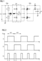
- FIG. 1 An embodiment of a resonant converter is shown by way of example and schematically, in which a functionality BU of a buck converter is integrated according to the invention.
- an input voltage Ue (direct voltage) is applied to the resonant converter, which can be related to a reference potential BP.
- An input capacitance Ce can also be arranged on the input side.
- two switching elements S1, S2 are connected in parallel to the input voltage Ue or the input capacitance Ce, which are arranged as a half-bridge circuit. This means that a first switching element S1 and a second switching element S2 are connected in series between a potential of the input voltage Ue and the reference potential BP.
- MOS-FETs, bipolar transistors or IGBTs can be used as switching elements S1, S2, for example.
- the resonant converter has a galvanic isolation, which separates the resonant converter into a primary side RWp and a secondary side RWs.
- a transformer is used as galvanic isolation, for example, which comprises a primary winding Wp on the primary side RWp and, for example, two secondary windings Ws1, Ws2 on the secondary side RWs.
- the secondary windings Ws1, Ws2 can be designed either as two separate coils Ws1, Ws2 or as a coil with a center tap, with the center tap dividing the coil into a first and a second secondary winding Ws1, Ws2.
- a rectifier unit is provided on the secondary side RWs, which comprises, for example, two diodes D1, D2.
- the rectifier unit rectifies an alternating voltage, into which the input voltage Ue applied to the primary side RWp is converted, on the secondary side RWs into a predeterminable output voltage Ua.
- an anode of a first diode D1 is connected to a connection of the first secondary winding Ws1 and an anode of a second diode D2 is connected to a connection of the second secondary winding Ws2.
- the cathodes of the diodes D1, D2 are connected to one another and form a first connection for a load.
- the second connection for the load is formed by the middle between the secondary windings Ws1, Ws2 or the center tap.
- the output voltage then falls at the connections.
- Ua of the resonant converter whereby an output capacitance Ca can be arranged in parallel.
- the output voltage Ua can also be related to the reference potential BP.
- a so-called synchronous rectifier with two controllable switching elements eg MOSFETs, gallium nitride switches, etc.
- the first diode D1 is replaced by a switching element and the second diode D2 by another switching element.
- only one secondary winding Ws1, Ws2 can be arranged on the secondary side, which is equipped with four rectifier diodes D1, D2, for example.
- Another design of the secondary side RWs can, for example, have several secondary windings Ws1, Ws2 with associated rectifier units.
- a center of the half-bridge circuit of the two switching elements S1, S2 is connected to a connection of the primary winding Wp of the transformer on the input side.
- the other connection of the primary winding Wp is connected to the resonance circuit of the resonance converter, which has at least one resonance inductance L and at least one resonance capacitance C1, C2.
- the resonance circuit can be formed from a stray inductance of the transformer as resonance inductance L and at least one resonance capacitance C1, C2.
- a first connection of the resonance inductance L is connected to the other connection of the primary winding Wp.
- a second connection of the resonance inductance L is connected to a center of a series circuit of two resonance capacitances C1, C2.
- a bidirectional switching element S3 is arranged in a current path i of a resonance current which flows through the resonance inductance L and at least one of the two resonance capacitances C1, C2.
- the bidirectional switching element S3 is inserted between the second connection of the resonance inductance L and the middle of the series connection of the two resonance capacitances C1, C2.
- the bidirectional switching element S3 can be constructed from anti-serially connected transistors (e.g. MOSFETs). Alternatively, a so-called micro-electronic-mechanical system, MEMS for short, can be used as the bidirectional switching element S3.
- MOSFETs anti-serially connected transistors
- MEMS micro-electronic-mechanical system
- a diode pair DB1, DB2 is provided, which is arranged as a series or series connection.
- a center of the series connection of the diode pair DB1, DB2 is connected to the second connection of the at least one resonance inductance L and to that connection of the bidirectional switching element S3 which is connected to the second connection of the at least one resonance inductance L.
- a respective end of the series connection of the diode pair DB1, DB2 is connected to a respective end of the series connection of the resonance capacitances C1, C2 and to an end of the half-bridge circuit of the primary-side switching elements S1, S2.
- a first diode DB1 of the diode pair DB1, DB2 is connected to a first resonance capacitance C1 and a first switching element S1 of the half-bridge circuit, with this connection forming, for example, a first connection for the input voltage Ue.
- a second diode DB2 of the diode pair DB1, DB2 is connected, for example, to a second resonance capacitance C2 and a second switching element S2 of the half-bridge circuit, whereby this connection forms, for example, a second connection for the input voltage Ue, which is related, for example, to the reference potential BP.
- the switching elements S1, S2 of the resonant converter arranged on the primary side are switched alternately with a short pause - a so-called dead time.
- the switching elements S1, S2 are each assigned a switching frequency in the form of of control signals (e.g. square-wave control signals).
- control signals e.g. square-wave control signals
- the bidirectional switching element S3 is permanently switched on.
- the bidirectional switching element S3 can be bridged or short-circuited by a bridging unit (eg semiconductor switch, relay, MEMS, etc.) in normal operation.
- a bridging unit eg semiconductor switch, relay, MEMS, etc.
- the circuit shown as an example can be considered as an LLC resonant converter, in which the second connection of the resonant inductance L is connected directly to the center of the series connection of the resonant capacitors C1, C2.
- the primary-side switching elements S1, S2 are ideally switched at the resonant frequency or the resonant converter operates in resonant mode.
- the bidirectional switching element S3 begins to switch within a half period of the switching frequency of the switching elements S1, S2.
- the control signal of the bidirectional switching element S3 is synchronized with the control signals of the switching elements S1, S2 in such a way that the bidirectional switching element S3 is switched on with the switching element S1, S2 to be switched on.
- a slight time offset - e.g. leading or lagging - can be provided between the switching on of the bidirectional switching element S3 and the switching element S1, S2 to be switched on, for example in order to divide or optimize switching losses.
- the bidirectional switching element S3 is controlled depending on the output voltage Ua of the resonance converter - ie pulse width modulated. This is subsequently determined using the Figure 2 explained in more detail.
- the bidirectional switching element S3 By switching the bidirectional switching element S3 on and off, the bidirectional switching element S3 together with the resonance inductance L and the diode pair DB1, DB2 form the functionality BU of a buck converter, with the diodes DB1, DB2 of the diode pair acting as freewheeling diodes.
- the input voltage Ue of the resonance converter is reduced for at least part of the half switching period of the switching element S1, S2 that is switched on at the time and the output voltage Ua is subsequently lowered.
- the switching elements S1, S2 of the half-bridge circuit continue to clock as in normal operation or in resonance operation with the resonance frequency of the resonance converter as the switching frequency.
- Figure 2 shows, by way of example, a time course of the control signals of the primary-side switching elements S1, S2 of the resonant converter and of the bidirectional switching element S3, which is arranged in the current path i of the resonant current flowing through the resonant inductance L and the resonant capacitances C1, C2, in the event that a reduction in the output voltage Ua of the resonant converter is required.
- the time t is plotted on a horizontal axis and the respective control signal voltage Sig on a vertical axis.
- a first time curve shows the control signal of the first switching element S1 of the half-bridge circuit and a second time curve shows the control signal of the second switching element S2 of the half-bridge circuit, whereby the dead times when switching the switching elements S1, S2 have not been plotted for the sake of simplicity.
- the control signals have the form of square-wave signals, for example.
- the switching elements S1, S2 are switched alternately.
- the first switching element S1 of the half-bridge circuit is switched on in a first half period HP1 of the control signal and switched off in a second half period HP2 of the control signal.
- the second switching element S2 of the half-bridge circuit is then switched off in the first half period HP1 of the control signal and switched on in the second half period HP2.
- the control signals for switching the switching elements S1, S2 are based on the switching frequency specified for the switching elements S1, S2, which corresponds to the resonance frequency of the resonant converter.
- the bidirectional switching element S3 is switched on as simultaneously as possible at a first point in time t1 with the start of the first half period HP1 of the control signal of the first switching element S1 or with the switching on of the first switching element S1 of the half-bridge circuit of the resonant converter.
- a bridging unit e.g. semiconductor switch, relay, MEMS, etc.
- a bridging unit that may be installed parallel to the bidirectional switching element S3 is opened in order to end the bridging of the bidirectional switching element S3.
- the resonant converter can operate at a significantly higher switching frequency (than the resonant frequency), at least for a short time.
- a significantly higher power loss as a result can be tolerated in this case, since the time voltage is rather short, in the range of a few milliseconds to, for example, a few 10 ms.
- the bidirectional switching element S3 is then switched off.
- the second time t2 is by a value of the output voltage Ua of the resonant converter to be reduced. This means that the bidirectional switching element S3 is voltage-controlled depending on the output voltage Ua or is controlled by pulse width modulation.
- the first switching element S1 of the half-bridge circuit remains switched on until a third time t3 - an end of the first half-period HP1. At the third time t3, the first switching element S1 of the half-bridge circuit is then also switched off.
- the resonant converter circuit arrangement operates as a pure resonant converter between the first and second points in time t1, t2.
- the energy stored in the resonant inductance L flows through the first diode DB1 of the diode pair DB1, DB2, which acts as a freewheeling diode, and through the primary winding Wp of the transformer, as a result of the bidirectional switching element S3 being switched off, whereby a current is induced in the first secondary winding Ws1 of the transformer on the secondary side RWs.
- the second switching element S2 of the half-bridge circuit is switched off during the entire first half period HP1.
- the second half-period HP2 of the control signals of the two switching elements S1, S2 of the half-bridge circuit begins.
- the second switching element S2 of the half-bridge circuit is switched on - delayed by a dead time (not shown).
- the bidirectional switching element S3 is switched on again at the third time t3.
- the bidirectional switching element S3 is then switched off again at a fourth time t4.
- the second switching element S2 of the half-bridge circuit remains switched on until a fifth time t5 - the end of the second half-period HP2.
- the second switching element S2 of the half-bridge circuit is then also switched off.
- the resonant converter circuit arrangement operates again as a pure resonant converter between the third and fourth times t3, t4.
- the energy stored in the resonant inductance L flows via the second diode DB2 of the diode pair DB1, DB2, which now functions as a freewheeling diode, and in turn via the primary winding Wp of the transformer, whereby a current is induced in the second secondary winding Ws2 of the transformer on the secondary side RWs.
- the first switching element S1 of the half-bridge circuit remains switched off throughout the second half-period HP2 and is only switched on again together with the bidirectional switching element S3 at the fifth time t5, which represents the start of the next, first half-period HP1, after a delay of a dead time (not shown).
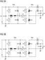
- Figure 3a shows a further embodiment of the resonant converter circuit arrangement according to the invention.
- An input voltage Ue is again applied to the input side of the circuit arrangement, which can be related to the reference potential BP.
- An input capacitance Ce is also provided on the input side.
- the circuit also comprises a galvanic isolation or a transformer with a primary winding Wp on the primary side RWp and secondary windings Ws1, Ws2 on the secondary side RWs.
- the circuit has a rectifier unit with two diodes D1, D2 on the secondary side RWs and an output capacitance Ca, across which the output voltage Ua drops.
- the output voltage Ua can also be related to the reference potential BP or, for example, float relative to the primary side RWp.
- two switching elements S1, S2 are arranged parallel to the input capacitance Ce, which are connected in series. Furthermore, two further switching elements S4, S5 are provided on the primary side, which are also arranged in series and connected to the two input-side Switching elements S1, S2 form a full-bridge circuit for controlling the resonant converter circuit arrangement. For this purpose, two of the four switching elements S1, S2, S4, S5 are switched on or off simultaneously. For example, switching elements S1, S5 or S2, S4 arranged diagonally opposite one another in the full-bridge circuit can be switched on or off simultaneously.
- a connection of the primary winding Wp is again connected to the middle of the series connection of the two input-side switching elements S1, S2 or a first half-bridge made up of the switching elements S1, S2 of the full-bridge circuit.
- the other connection of the primary winding Wp is connected to the resonant circuit, which is formed by a resonant inductance L and a resonant capacitance C.
- the first connection of the resonant inductance L is connected to the primary winding Wp and the second connection of the resonant inductance L is connected to a first connection of the resonant capacitance C.
- the bidirectional switching element S3 is arranged between a second connection of the resonant capacitance C and a middle of the series connection of the two further switching elements S4, S5 in the current path i of the resonant current through the resonant inductance L and through the resonant capacitance C.
- This means that the bidirectional switching element S3 is connected with the first terminal to the second terminal of the resonance capacitance C and with the second terminal to the center of the series circuit consisting of the two further primary-side switching elements S4, S5, which forms a second half-bridge for the full-bridge circuit.
- a diode pair DB1, DB2 is also provided.
- the two diodes DB1, DB2 of the diode pair DB1, DB2 are arranged in series and act as freewheeling diodes DB1, DB2 for the integrated functionality of the buck converter.
- a center of the series connection of the diode pair DB1, DB2 is connected to the second connection of the resonance inductance L and to the first connection of the resonance capacitance C.
- the respective ends of the series connection of the diode pair DB1, DB2 are each connected to the corresponding ends of the two half bridges of the full bridge circuit, which are formed by the two input-side switching elements S1, S2 or the two further switching elements S4, S5.
- the bidirectional switching element S3 In normal operation - i.e. in operation with nominal voltage - the bidirectional switching element S3 is either permanently switched on again or bridged or short-circuited by a bridging unit (semiconductor switch, relay, MEMS, etc.) arranged parallel to the bidirectional switching element S3. The circuit then works as a resonant converter in resonance mode. If the output voltage Ua of the resonant converter needs to be reduced, the bidirectional switching element S3 is controlled - pulse width modulated or depending on the output voltage Ua.
- a bridging unit semiconductor switch, relay, MEMS, etc.
- the bidirectional switching element S3 is switched on again synchronously with the switching elements S1, S5 or S2, S4 to be switched on and switched off before the switching elements S1, S5 or S2, S4 that are switched on in order to integrate the BU functionality of a buck converter into the resonant converter.
- Figure 3b shows a further embodiment of the resonant converter circuit arrangement according to the invention with a full-bridge circuit for control, wherein the full-bridge circuit is again formed by the two switching elements S1, S2 arranged on the input side and two further switching elements S4, S5 on the primary side.
- This embodiment differs from the one in Figure 3a shown circuit arrangement only by the arrangement of the diode pair DB1, DB2 in the circuit.
- the resonance capacitance C is again connected to the first terminal with the resonance inductance L.
- the middle of the series connection of the diode pair DB1, DB2 is now connected to the second terminal of the resonance capacitance C and to the first terminal of the bidirectional switching element S3.
- the ends of the series connection of the diode pair DB1, DB2 are again connected to the respective ends of the two half bridges of the full bridge circuit, which are formed by the two input-side switching elements S1, S2 and the two further switching elements S4, S5.
Landscapes
- Engineering & Computer Science (AREA)
- Power Engineering (AREA)
- Dc-Dc Converters (AREA)
Description
- Die gegenständliche Erfindung betrifft allgemein das Gebiet der Elektrotechnik, insbesondere den Bereich der Leistungselektronik und leistungselektronischer Schaltungen zur Stromversorgung. Im Speziellen bezieht sich die vorliegende Erfindung auf eine Schaltungsanordnung für einen Resonanzwandler. Der Resonanzwandler weist eine galvanische Trennung, insbesondere einen Transformator, auf. Weiterhin umfasst der Resonanzwandler primärseitig zumindest eine Resonanzinduktivität, zumindest eine Resonanzkapazität und zumindest zwei Schaltelemente, welchen jeweils einen Schaltfrequenz vorgegeben wird. Dabei fließt durch ein Schalten der zumindest zwei, primärseitig angeordneten Schaltelemente mit der jeweils vorgegebenen Schaltfrequenz ein Resonanzstrom durch die zumindest eine Resonanzinduktivität und durch die zumindest eine Resonanzkapazität.
- Heutzutage werden in modernen Stromversorgungen für elektrische Geräte immer häufiger Resonanzwandler (im Englischen auch als "resonant converter" bezeichnet) zur Energieübertragung eingesetzt. Resonanzwandler stellen eine spezielle schaltungstechnische Form eines Gleichspannungswandlers dar, welcher zur Energieübertragung mit einem Schwingkreis bzw. Resonanzkreis arbeitet. Dabei wandelt der Resonanzwandler eine eingangsseitige Gleichspannung in eine ein- oder mehrphasige Wechselspannung um, wobei er für einen optimalen Betrieb typischerweise mit annähernd konstanter Last betrieben wird. Die Wechselspannung kann durch eine ausgangsseitig angeordnete Gleichrichtereinheit wieder in eine vorgebbare Ausgangsspannung gleichgerichtet werden. Erfolgt keine Gleichrichtung auf der Ausgangsseite des Resonanzwandlers, so bezeichnet man den Resonanzwandler auch als Wechselrichter oder Inverter.
- Der bekannte Stand der Technik auf diesem Gebiet wird durch die Dokumente
US 2021/058004 A1 undUS 2015/049520 A1 gebildet. - Aus dem Dokument
US 2021/058004 A1 ist ein Gleichspannungswandler in Serie mit einem Aufwärtswandler bekannt. - Aus dem Dokument
US 2015/049520 A1 ist ein Resonanzwandler mit einer Schaltungsanordnung zur Reduzierung der Resonanzkapazitätsspannung im Falle eines Überstroms bekannt. - Üblicherweise ist bei einem Resonanzwandler der Resonanzkreis aus zumindest einer Resonanzkapazität und zumindest einer Resonanzinduktivität aufgebaut. Der Resonanzkreis kann beispielsweise je nach Schaltungsaufbau auf einer Primär- oder Sekundärseite einer verwendeten galvanischen Trennung bzw. eines Transformators angeordnet und als Serien- oder Parallelschwingkreis aufgebaut sein. Üblicherweise wird der Resonanzkreis von der leistungsübertragenden Strecke mit der galvanischen Trennung bzw. mit dem Transformator gemeinsam mit zumindest eine Resonanzkapazität gebildet, wobei als Resonanzinduktivität z.B. die Streuinduktivität des Transformators allein oder die Streuinduktivität des Transformators gemeinsam mit zumindest einer weiteren Induktivität verwendet werden kann. Je nach Anwendung können damit Resonanzwandler z.B. als so genannte LLC-(=LCL)- oder LCC-Konverter ausgebildet sein.
- Zur Regelung der Ausgangsspannung werden Resonanzwandler üblicherweise mit festem Tastverhältnis und variabler Frequenz bzw. Schaltfrequenz angesteuert. Die Schaltfrequenz dient als Basis für die Steuersignale zum Schalten der zumindest zwei, primärseitigen Schaltelemente, wodurch ein Resonanzstrom durch den Resonanzkreis fließt. Dabei entspricht eine Pulslänge des Steuersignals (z.B. Rechteck-Signal) des jeweiligen Schaltelements im Wesentlichen einer halben Schwingungsdauer des Resonanzkreises, um ein Einschalten und Ausschalten der zumindest zwei primärseitigen Schaltelemente in einem Schwingungsnulldurchgang Stroms oder der Spannung) - d.h. um so genanntes Zero Voltage Switching (kurz: ZVS) oder so genanntes Zero Current Switching (kurz: ZCS) zu ermöglichen. Es kann z.B. zwischen Resonanzwandlern mit Zero Voltage Switching und Resonanzwandler mit Zero Current Switching unterschieden werden, wobei meist beides zusammenfällt. Das bedeutet, dass der Bereich der Schaltfrequenz, welche jeweils den primärseitigen Schaltelementen vorgegeben wird bzw. mit welcher diese geschaltet werden können, durch den Resonanzkreis - insbesondere durch die zumindest eine Resonanzinduktivität und durch die zumindest eine Resonanzkapazität des Resonanzwandlers - mitbestimmt wird. Der Resonanzkreis sorgt bei einem Resonanzwandler üblicherweise dafür, dass die Schaltelemente im Wesentlichen im Strom- und/oder Spannungsnulldurchgang geschaltet werden. Dadurch werden während der Schaltvorgänge die Verlustleistung minimiert sowie elektromagnetische Störungen geringgehalten.
- Resonanzwandler weisen aufgrund ihrer frequenzabhängigen Komponenten, wie z.B. Transformator, Kapazitäten und gegebenenfalls zusätzliche Induktivitäten, ein frequenzabhängiges Spannungsübersetzungsverhältnis zwischen Ausgangsspannung und Eingangsspannung auf. Durch beispielsweise entsprechende Wahl der Windungszahlen des im Resonanzwandler eingesetzten Transformators kann dieses Übersetzungsverhältnis weiter angepasst werden. Dieses Übersetzungsverhältnis ist jedoch bis auf eine spezielle Schaltfrequenz lastabhängig. Da Resonanzwandler in der Regel aus zwei oder mehreren frequenzabhängigen Komponenten (z.B. Kondensatoren, Spulen, Transformatoren, etc.) bestehen, gibt es oft mehrere Resonanzfrequenzen, wobei meist nur bei einer bestimmten Resonanzfrequenz ein lastunabhängiges Übersetzungsverhältnis auftritt. Diese bestimmte Resonanzfrequenz ist die Frequenz, welche bei der Resonanz der Resonanzinduktivität und der Resonanzkapazität auftritt und nicht bei einer geringen Resonanzfrequenz von Transistor-Hauptinduktivität plus Resonanzinduktivität und der Resonanzkapazität. Nur bei einem Betrieb mit exakt dieser Resonanzfrequenz (d.h. der Resonanzfrequenz, welche von Resonanzinduktivität und Resonanzkapazität festgelegt wird) als Schaltfrequenz für primärseitigen Schaltelemente sind die Schaltverluste des Resonanzwandlers nahezu null bzw. sehr gering. Der Resonanzwandler arbeitet dann mit einem sehr hohen Wirkungsgrad und am effizientesten und weist bei der Resonanzfrequenz ein fast konstantes Übersetzungsverhältnis zwischen Eingangsspannung und Ausgangsspannung auf, welches sich nur am Windungszahlverhältnis zwischen Primär- und Sekundärwicklungen des verwendeten Transformators orientiert.
- Bei einem Überlastfall (z.B. Überlast, Kurzschluss, etc.) kann es allerdings notwendig sein, die Ausgangsspannung des Resonanzwandlers abzusenken, um beispielsweise eine geforderte Strom-Spannungs-Kennlinie für einen Strombegrenzung bzw. bis zum Kurzschluss zu gewährleisten. Um eine derartige, notwendige Absenkung der Ausgangsspannung des Resonanzwandlers zu erreichen, kann beispielsweise die Schaltfrequenz bzw. Arbeitsfrequenz des Resonanzwandlers über die Resonanzfrequenz hinaus angehoben werden. D.h., die primärseitigen Schaltelemente werden mit einer höheren Schaltfrequenz als mit der Resonanzfrequenz betrieben. Dabei weicht der Resonanzwandler vom idealen Betrieb mit der Resonanzfrequenz ab. Es entstehen dadurch höhere Verluste - trotz einer sinkenden Ausgangsleistung. Durch die höhere Schaltfrequenz können z.B. die primärseitigen Schaltelemente nicht mehr im Spannungsnulldurchgang (so genanntes Zero Voltage Switching oder ZVS) oder im Stromnulldurchgang (so genanntes Zero Current Switching oder ZCS) geschalten werden, sondern werden beispielsweise "hart" ein-und ausgeschaltet, was eine erhebliche Verlustleistung in den Schaltelementen zur Folge hat. Weiterhin entstehen durch die Steigerung der Schaltfrequenz beispielsweise auch erhöhte Verluste am Transformator, an einer gegebenenfalls vorhandenen zusätzlichen Resonanzinduktivität sowie an einer sekundärseitig angeordneten Gleichrichtereinheit (z.B. Dioden, Synchron-Gleichrichter).
- Um massiv steigende Verluste im Resonanzwandler bei Absenkung der Ausgangsspannung durch Anheben der Schaltfrequenz über die Resonanzfrequenz hinaus zu verhindern, besteht beispielsweise die Möglichkeit, dem Resonanzwandler eingangsseitig eine zusätzlich Wandler-Stufe, insbesondere einen Tiefsetzsteller, vorzuschalten. Durch Vorschalten der zusätzlichen Wandler-Stufe bzw. eines Tiefsetzsteller wird sichergestellt, dass der Resonanzwandler wieder mit einem fixen Übersetzungsverhältnis bzw. möglichst im Resonanzbetrieb arbeiten kann, indem durch die vorgeschaltete Wandler-Stufe die Eingangsspannung des Resonanzwandler entsprechend zur abgesenkten Ausgangsspannung des Resonanzwandlers eingestellt wird. Allerdings ist das Vorschalten der zusätzlichen Wandler-Stufe mit erhöhtem Platzbedarf und Kosten verbunden. Weiterhin ist diese zusätzliche Wandler-Stufe nicht nur z.B. im Überlastfall im Betrieb, sondern auch dann, wenn der Resonanzwandler im Normalbetrieb mit der Resonanzfrequenz bzw. bei Nennlast betrieben wird. Dadurch entsteht während des Normalbetriebs des Resonanzwandlers eine unnötige Verlustleistung durch die vorgeschaltete Wandler-Stufe.
- Der Erfindung liegt daher die Aufgabe zugrunde, eine Schaltungsanordnung für einen Resonanzwandler anzugeben, welche für einen Überlastfall eine Reduktion der Ausgangsspannung auf effiziente und platzsparende Weise und ohne zusätzliche Verlustleistung ermöglicht.
- Diese Aufgabe wird durch eine Schaltungsanordnung für einen Resonanzwandler gemäß dem unabhängigen Anspruch gelöst. Vorteilhafte Ausführungsformen der vorliegenden Erfindung sind in den abhängigen Ansprüchen beschrieben.
- Erfindungsgemäß erfolgt die Lösung der Aufgabe durch eine Schaltungsanordnung eines Resonanzwandler der eingangs erwähnten Art, bei welcher ein bidirektionales Schaltelement in einem Strompfad des Resonanzstroms durch die zumindest eine Resonanzinduktivität und durch die zumindest eine Resonanzkapazität angeordnet ist. Weiterhin ist ein Diodenpaar vorgesehen, welches als Reihen- bzw. Serienschaltung angeordnet ist. Dabei ist eine Mitte der Serienschaltung des Diodenpaars mit einem Anschluss der zumindest einen Resonanzinduktivität oder mit einem Anschluss der zumindest einen Resonanzkapazität und ein jeweiliges Ende der Serienschaltung des Diodenpaars mit jeweils einem Schaltelement der zumindest zwei primärseitigen Schaltelemente derart verbunden sind, dass eine Funktionalität eines Tiefsetzstellers integriert ist, in dem Fall dass das bidirektionale Schaltelement synchronisiert bzw. annähernd zeitgleich mit einem jeweils einzuschaltenden Schaltelement der zumindest zwei primärseitigen Schaltelemente eingeschaltet wird und vor einem jeweils auszuschaltenden Schaltelement der zumindest zwei primärseitigen Schaltelemente ausgeschaltet wird. Dabei sind die zumindest eine Resonanzinduktivität als Induktivität und das Diodenpaars als Freilaufdioden für die Funktionalität des Tiefsetzstellers genutzt.
- Der Hauptaspekt der erfindungsmäßig vorgeschlagenen Lösung besteht darin, dass ein Hinzufügen eines bidirektionalen Schaltelements und des Diodenpaars und durch entsprechendes Schalten des bidirektionalen Schaltelements - d.h. ein mit dem jeweils für die Ansteuerung des Resonanzwandlers einzuschaltenden Schaltelement synchronisierten Einschalten des bidirektionalen Schaltelements, aber ein Ausschalten vor dem jeweils eingeschalteten Schaltelements für die Ansteuerung des Resonanzwandlers - auf einfache Weise eine Funktionalität eines Tiefsetzsteller - sowohl für positive als auch für negative Stromhalbwellen - in den Resonanzwandler integriert wird. Das bedeutet, es wird eine Funktionalität eines Tiefsetzstellers in den Resonanzwandler integriert, durch welche ein Betrag einer Ausgangsspannung stets kleiner als ein Betrag einer Eingangsspannung ist bzw. ein Übersetzungsverhältnis des Resonanzwandlers verändert wird. D.h. wird das im Strompfad des Resonanzstroms angeordnete, bidirektionale Schaltelement geschaltet, so bildet das bidirektionale Schaltelement gemeinsam mit der zumindest einen Resonanzinduktivität und dem Diodenpaar als Freilaufdioden einen Tiefsetzsteller, durch welchen die Aufgabe erfüllt wird, im Bedarfsfall (z.B. bei Überlast, Kurzschluss, etc.) eine am Resonanzwandler anliegende Eingangsspannung zumindest für Teile der Schaltperiode des Resonanzwandlers abzusenken und damit die Ausgangsspannung zu reduzieren. Die zumindest zwei, primärseitigen Schaltelemente zur Ansteuerung des Resonanzwandlers können idealerweise auch im Überlastfall mit der Resonanzfrequenz als Schaltfrequenz (d.h. wie im Normalbetrieb bzw. im Resonanzbetrieb) getaktet werden, wodurch die Schaltverluste weiterhin möglichst gering bleiben.
- Durch die erfindungsgemäße Schaltungsanordnung kann eine dem Resonanzwandler vorgeschaltete Wandler-Stufe bzw. Tiefsetzsteller-Stufe sowie eine der Wandler-Stufe nachgeschaltete bzw. dem Resonanzwandler vorgeschaltete Zwischenkreiskapazität eingespart werden. Dadurch wird auch ein besserer Wirkungsgrad erzielt, da eine Verlustleistung einer vorgelagerten Tiefsetzsteller-Stufe wegfällt. Weiterhin kann die Schaltungsanordnung durch den Wegfall der Tiefsetzsteller-Stufe, insbesondere einer Drossel des Tiefsetzstellers, sowie der Zwischenkreiskapazität platzsparender ausgeführt sein.
- Es ist vorteilhaft, wenn das bidirektionale Schaltelement in Anhängigkeit von einer Ausgangsspannung des Resonanzwandlers gesteuert wird. D.h. das bidirektionale Schaltelement wird - sofern es taktet - idealerweise pulsweitenmoduliert bzw. mit konstanter Frequenz und veränderlichen Tastgrad des Steuersignals geschaltet. Das bidirektionale Schaltelement wird idealerweise synchronisiert mit dem jeweils einzuschaltenden, primärseitigen Schaltelement eingeschaltet. D.h., das bidirektionale Schaltelement wird möglichst zeitgleich bzw. maximal zeitlich geringfügig versetzt mit dem jeweils einzuschaltenden Schaltelement des Resonanzwandlers eingeschaltet. Ein Ausschaltzeitpunkt des bidirektionalen Schaltelements kann durch die spannungsabhängige Ansteuerung allerdings derart in einer halben Schaltperiode des jeweils einzuschaltenden Schaltelements festgelegt werden, dass eine Reduktion auf einen z.B. vorgebbaren Wert der Ausgangsspannung des Resonanzwandlers erreicht wird. So kann z.B. durch rascheres Ausschalten des bidirektionalen Schaltelements eine stärkere Reduktion erzielt werden, als wenn dieses länger eingeschalten bleibt.
- Es ist günstig, wenn während eines Normalbetriebs des Resonanzwandlers das bidirektionale Schaltelement dauerhaft eingeschaltet ist. Auf diese einfache Weise ist die Funktionalität des Tiefsetzstellers weggeschaltet. Die Schaltungsanordnung arbeitet als Resonanzwandler im Normalbetrieb bzw. im Resonanzbetrieb.
- Alternativ ist idealerweise eine Überbrückungseinheit vorgesehen ist, welche parallel zum bidirektionalen Schaltelement angeordnet ist. Durch Schließen der Überbrückungseinheit ist das bidirektionale Schaltelement überbrückt bzw. kurzgeschlossen. D.h., arbeitet die Schaltungsanordnung als Resonanzwandler im Normal- bzw. Resonanzbetrieb, so ist die Überbrückungseinheit geschlossen und das bidirektionale Schaltelement kann ausgeschaltet sein. Dadurch werden auf einfache Weise Leitverluste, welche durch ein dauerhaft eingeschaltetes, bidirektionales Schaltelement entstehen würden, gesenkt. Sollte ein Überlastfall eintreten, welcher eine Absenkung der Ausgangsspannung erfordert, so kann beispielsweise bis zum Öffnen der Überbrückungseinheit die den primärseitigen Schaltelementen vorgegebene Schaltfrequenz kurzfristig erhöht werden. Ist die Überbrückungseinheit ausgeschaltet und beginnt das bidirektionale Schaltelement zu schalten, so können die primärseitigen Schaltelemente wieder mit der Resonanzfrequenz als Schaltfrequenz angesteuert werden. Als Überbrückungseinheit ist ein Halbleiterschalter, ein Relais oder ein so genanntes Mikro-Elektronisch-Mechanisches-System, kurz MEMS, einsetzbar.
- Eine vorteilhafte Ausführungsform der Schaltanordnung sieht vor, dass die zumindest zwei primärseitigen Schaltelemente eingangsseitig als Halbbrückenschaltung angeordnet sind. Die Ausführung als Halbbrückenschaltung umfasst zwei Schaltelemente, welche z.B. mittels entsprechender Ansteuerschaltungen alternierend bzw. abwechselnd mit einer kurzen Pause (Totzeit) schalten. Dabei ist für die Integration der Funktionalität des Tiefsetzstellers die Mitte der Serienschaltung des Diodenpaars mit einem Anschluss der zumindest einen Resonanzinduktivität verbunden, welcher einem ersten Ende des bidirektionalen Schaltelements verbunden ist. Weiterhin weist die zumindest eine Resonanzkapazität durch zwei in Serie angeordnete Kapazitäten auf, wobei eine Mitte der Serienschaltung der zwei Kapazitäten mit einem zweiten Ende des bidirektionalen Schaltelements und die jeweiligen Enden der Serienschaltung der zwei Kapazitäten mit den jeweiligen Enden der Serienschaltung des Diodenpaars verbunden sind.
- Eine zweckmäßige Ausgestaltung der erfindungsgemäßen Schaltungsanordnung sieht primärseitig zwei weitere Schaltelemente vorgesehen sind, welche mit den zumindest zwei primärseitigen Schaltelementen als Vollbrückenschaltung angeordnet sind. Bei einer Vollbrückenschaltung kommen üblicherweise vier Schaltelemente mit entsprechender Ansteuerschaltung zum Einsatz. Es werden immer zwei Schaltelemente gleichzeitig eingeschaltet (z.B. immer die diagonal gegenüberliegenden), darauf folgt eine Totzeit, dann werden die beiden anderen Schaltelemente eingeschaltet. Während die Halbbrückenschaltung einfacher aufgebaut und kostengünstiger ist, hat eine Vollbrückenschaltung den Vorteil der geringeren Strombelastung der Schaltelemente im Vergleich zur Halbbrückenschaltung, dies bringt zwar geringere Verluste, aber im Regelfall überwiegen die Vorteile einer Vollbrückenschaltung erst bei hohen Leistungen von deutlich >1kW.
- Eine spezielle Ausführungsform der Schaltungsanordnung bei Verwendung einer Vollbrückenschaltung sieht vor, dass die Mitte der Serienschaltung des Diodenpaars mit einem Anschluss der zumindest einen Resonanzinduktivität verbunden ist, welcher an einen ersten Anschluss der zumindest einen Resonanzkapazität angebunden ist. Weiterhin ist ein zweiter Anschluss der zumindest einen Resonanzkapazität mit einem ersten Anschluss des bidirektionalen Schaltelements verbunden. Es ist an einen zweiten Anschluss des bidirektionalen Schaltelements eine Mitte einer Serienschaltung aus den zwei, weiteren primärseitigen Schaltelementen angebunden. Weiterhin sind die jeweiligen Enden der Serienschaltung des Diodenpaars jeweils mit einem Schaltelement der zumindest zwei primärseitigen Schaltelemente sowie jeweils mit einem der zwei, weiteren primärseitigen Schaltelemente verbunden.
- Alternativ kann die Schaltungsanordnung bei Verwendung einer Vollbrückenschaltung idealerweise derart ausgestaltet sein, dass die zumindest eine Resonanzkapazität mit einem ersten Anschluss an die zumindest eine Resonanzinduktivität angebunden ist. Weiterhin ist ein zweiter Anschluss der Resonanzkapazität mit einem ersten Anschluss des bidirektionalen Schaltelements und mit der Mitte der Serienschaltung des Diodenpaars verbunden. An einen zweiten Anschluss des bidirektionalen Schaltelements ist eine Mitte einer Serienschaltung bzw. Halbbrückenschaltung aus den zwei, weiteren primärseitigen Schaltelementen angebunden. Weiterhin sind wieder die jeweiligen Enden der Serienschaltung des Diodenpaars jeweils mit einem Schaltelement der zumindest zwei primärseitigen Schaltelemente sowie jeweils mit einem der zwei, weiteren primärseitigen Schaltelemente verbunden.
- Es ist weiterhin vorteilhaft, wenn das bidirektionale Schaltelement aus antiseriell verschalteten Transistoren, insbesondere von Feldeffekttransistoren oder MOSFETs, aufgebaut ist. Dabei bezeichnet der Begriff "antiseriell" einen Reihenschaltung von Transistoren, insbesondere Feldeffekttransistoren, in entgegengesetzter Polung. D.h., dass z.B. ein Sourceanschluss eines ersten Feldeffekttransistors mit einem Sourceanschluss eines zweiten Feldeffekttransistors leitungstechnisch verbunden ist. Ferner ist es möglich, dass ein Drainanschluss des ersten Feldeffekttransistors mit einem Drainanschluss des zweiten Feldeffekttransistors leitungstechnisch verbunden ist. Eine derartige, antiserielle Verschaltung von Transistoren ist beispielsweise aus der Schrift
EP 1 850 470 B1 bekannt. - Alternativ kann es zweckmäßig sein, wenn als bidirektionales Schaltelement ein Mikro-Elektronisch-Mechanisches-System, kurz MEMS, vorgesehen ist. Ein MEMS stellt einen elektronischen Schalter dar, welche sehr einfach von einer Steuereinheit angesteuert werden kann, um einen Stromfluss zu begrenzen und/oder zu schalten. MEMS sind üblicherweise winzige Halbleiterbauelemente, welche idealerweise Logikelemente und mikromechanische Strukturen (z.B. Anker, welche über elektrostatische Kräfte bewegt werden) in einem Bauelement vereinen.
- Die Erfindung wird nachfolgend in beispielhafter Weise anhand der beigefügten Figuren erläutert. Es zeigen dabei:
-
Figur 1 in schematischer und beispielhafter Weise ein Schaltungsanordnung eines erfindungsgemäßen Resonanzwandlers -
Figur 2 beispielhaft einen zeitlichen Verlauf der Steuersignale der Schaltelemente der erfindungsgemäßen Resonanzwandler-Schaltungsanordnung -
Figur 3a und 3b beispielhaft und schematisch weitere Ausführungsformen der erfindungsgemäßen Schaltungsanordnung eines Resonanzwandlers - In
Figur 1 ist beispielhaft und schematisch eine Ausführungsform eines Resonanzwandlers dargestellt, in welchen erfindungsgemäß eine Funktionalität BU eines Tiefsetzsteller integriert ist. - Eingangsseitig wird eine Eingangsspannung Ue (Gleichspannung) an den Resonanzwandler angelegt, welche auf ein Bezugspotential BP bezogen sein kann. Es kann eingangsseitig auch eine Eingangskapazität Ce angeordnet sein. Weiterhin sind parallel zur Eingangsspannung Ue bzw. zur Eingangskapazität Ce zwei Schaltelemente S1, S2 geschaltet, welche als Halbbrückenschaltung angeordnet sind. D.h. ein erstes Schaltelement S1 und ein zweites Schaltelement S2 sind zwischen einem Potential der Eingangsspannung Ue und dem Bezugspotential BP in Reihe bzw. in Serie geschaltet. Als Schaltelemente S1, S2 sind beispielsweise MOS-FETs, bipolare Transistoren oder IGBTs einsetzbar.
- Der Resonanzwandler weist eine galvanischer Trennung auf, welche den Resonanzwandler in eine Primärseite RWp und in eine Sekundärseite RWs trennt. Als galvanische Trennung wird z.B. ein Transformator verwendet, welcher eine Primärwicklung Wp auf der Primärseite RWp und z.B. zwei Sekundärwicklungen Ws1, Ws2 auf der Sekundärseite RWs umfasst. Die Sekundärwicklungen Ws1, Ws2 können entweder als zwei getrennte Spulen Ws1, Ws2 oder als eine Spule mit Mittelanzapfung ausgeführt sein, wobei die Mittelanzapfung die Spule in eine erste und in eine zweite Sekundärwicklung Ws1, Ws2 unterteilt.
- Weiterhin ist auf der Sekundärseite RWs eine Gleichrichtereinheit vorgesehen, welche beispielsweise zwei Dioden D1, D2 umfasst. Durch die Gleichrichtereinheit wird aus einer Wechselspannung, in welche die an der Primärseite RWp anliegende Eingangsspannung Ue umgewandelt wird, auf der Sekundärseite RWs in eine vorgebbare Ausgangsspannung Ua gleichgerichtet. Dazu ist eine Anode einer ersten Diode D1 an einen Anschluss der ersten Sekundärwicklung Ws1 und eine Anode einer zweiten Diode D2 an einen Anschluss der zweiten Sekundärwicklung Ws2 angebunden. Die Kathoden der Dioden D1, D2 sind miteinander verbunden und bilden eine ersten Anschluss für eine Last. Der zweite Anschluss für die Last wird von der Mitte zwischen den Sekundärwicklungen Ws1, Ws2 bzw. der Mittelanzapfung gebildet. An den Anschlüssen fällt dann die Ausgangsspannung Ua des Resonanzwandlers ab, wobei parallel dazu eine Ausgangskapazität Ca angeordnet sein kann. Die Ausgangsspannung Ua kann ebenfalls auf das Bezugspotential BP bezogen sein. Alternativ kann zu einer Gleichrichtereinheit mit zwei Dioden D1, D2 kann auch ein so genannter Sychrongleichrichter mit zwei ansteuerbaren Schaltelementen (z.B. MOSFETs, Galliumnitrid-Schaltern, etc.) verwendet werden, wobei die erste Diode D1 durch ein Schaltelement und die zweite Diode D2 durch ein weiteres Schaltelement ersetzt wird.
- Alternativ kann sekundärseitig auch nur eine Sekundärwicklung Ws1, Ws2 angeordnet sein, welche z.B. mit vier Gleichrichterdiode D1, D2 ausgestattet ist. Eine weitere Ausführung der Sekundärseite RWs kann beispielsweise mehrere Sekundärwicklungen Ws1, Ws2 mit zugehörigen Gleichrichtereinheiten aufweisen.
- Auf der Primärseite RWp ist eingangsseitig eine Mitte der Halbbrückenschaltung der zwei Schaltelemente S1, S2 mit einem Anschluss der Primärwicklung Wp des Transformators verbunden. Der andere Anschluss der Primärwicklung Wp ist mit dem Resonanzkreis des Resonanzwandler verbunden, welcher zumindest eine Resonanzinduktivität L und zumindest eine Resonanzkapazität C1, C2 aufweist. Im einfachsten Fall kann der Resonanzkreis aus einer Streuinduktivität des Transformators als Resonanzinduktivität L und zumindest einer Resonanzkapazität C1, C2 gebildet werden.
- Bei der in
Figur 1 beispielhaft dargestellten Ausführungsform der erfindungsgemäßen Schaltungsanordnung ist an den anderen Anschluss der Primärwicklung Wp ein erster Anschluss der Resonanzinduktivität L angebunden. Ein zweiter Anschluss der Resonanzinduktivität L ist mit einer Mitte einer Serienschaltung aus zwei Resonanzkapazitäten C1, C2 verbunden. Dabei ist in einem Strompfad i eines Resonanzstroms, welcher durch die Resonanzinduktivität L und zumindest eine der zwei Resonanzkapazitäten C1, C2 fließt, ein bidirektionales Schaltelement S3 angeordnet. Bei der inFigur 1 beispielhaft dargestellten Ausführungsform ist das bidirektionale Schaltelement S3 z.B. zwischen dem zweiten Anschluss der Resonanzinduktivität L und der Mitte der Serienschaltung der zwei Resonanzkapazitäten C1, C2 eingefügt. Das bidirektionale Schaltelement S3 kann dabei z.B. aus antiseriell verschalteten Transistoren (z.B. MOSFETs) aufgebaut sein. Alternativ kann z.B. ein so genanntes Mikro-Elektronisch-Mechanisches-System, kurz MEMS, als bidirektionales Schaltelement S3 eingesetzt werden. - Weiterhin ist ein Diodenpaar DB1, DB2 vorgesehen, welches als Reihen- bzw. Serienschaltung angeordnet ist. Eine Mitte der Serienschaltung des Diodenpaars DB1, DB2 ist mit dem zweiten Anschluss der zumindest einen Resonanzinduktivität L sowie mit jenem Anschluss des bidirektionalen Schaltelements S3 verbunden, welches an den zweiten Anschluss der der zumindest einen Resonanzinduktivität L angebunden ist. Ein jeweiliges Ende der Serienschaltung des Diodenpaars DB1, DB2 ist jeweils mit einem jeweils entsprechenden Ende der Serienschaltung der Resonanzkapazitäten C1, C2 sowie jeweils mit einem Ende der Halbbrückenschaltung der primärseitigen Schaltelemente S1, S2 verbunden. Dabei ist beispielsweise eine erste Diode DB1 des Diodenpaars DB1, DB2 mit einer ersten Resonanzkapazität C1 und einem ersten Schaltelement S1 der Halbbrückenschaltung verbunden, wobei von dieser Verbindung z.B. ein erster Anschluss für die Eingangsspannung Ue gebildet wird. Eine zweite Diode DB2 des Diodenpaars DB1, DB2 ist beispielsweise mit einer zweiten Resonanzkapazität C2 und einem zweiten Schaltelement S2 der Halbbrückenschaltung verbunden, wobei von dieser Verbindung z.B. ein zweiter Anschluss für die Eingangsspannung Ue gebildet wird, welcher beispielsweise auf das Bezugspotential BP bezogen ist.
- Um die Eingangsspannung Ue in die vorgebbare Ausgangsspannung Ua auf der Sekundärseite RWs umzuwandeln, werden die primärseitig angeordneten Schaltelemente S1, S2 des Resonanzwandlers abwechselnd mit einer kurzen Pause - einer so genannten Totzeit - geschaltet. Für ein entsprechendes Takten wird den Schaltelementen S1, S2 jeweils eine Schaltfrequenz in Form von Steuersignalen (z.B. rechteckförmige Steuersignale) vorgegeben. Dadurch werden die Schaltelemente S1, S2 der Halbbrückenschaltung alternierend mit einer kurzen Pause bzw. Totzeit ein- und jeweils in einem Strom- und/oder Spannungsnulldurchgang ausgeschaltet.
- Weiterhin ist im Normalbetrieb des Resonanzwandlers - d.h. im Betrieb bei Nennlast - das bidirektionale Schaltelement S3 dauerhaft eingeschaltet. Alternativ kann das bidirektionale Schaltelement S3 im Normalbetrieb durch eine Überbrückungseinheit (z.B. Halbleiterschalter, Relais, MEMS, etc.) überbrückt bzw. kurzgeschlossen sein. D.h. die in
Figur 1 beispielhaft dargestellte Schaltung kann als LLC-Resonanzwandler betrachtet werden, bei welchem der zweite Anschluss der Resonanzinduktivität L direkt an die Mitte der Serienschaltung der Resonanzkapazitäten C1, C2 angebunden ist. Die primärseitigen Schaltelemente S1, S2 werden idealerweise mit der Resonanzfrequenz geschaltet bzw. der Resonanzwandler arbeitet im Resonanzbetrieb. - Tritt allerdings ein Ereignis (z.B. Überlast, Kurzschluss, etc.) ein, bei welchem eine Absenkung der Ausgangsspannung Ua erforderlich ist, so beginnt das bidirektionale Schaltelement S3 innerhalb einer Halbperiode der Schaltfrequenz der Schaltelemente S1, S2 zu schalten. Dabei ist das Steuersignal des bidirektionalen Schaltelements S3 mit den Steuersignalen der Schaltelemente S1, S2 derart synchronisiert, dass das bidirektionale Schaltelement S3 mit dem jeweils einzuschaltenden Schaltelement S1, S2 eingeschaltet wird. Dabei kann ein geringfügiger Zeitversatz - z.B. voreilend oder nacheilend - zwischen dem Einschalten des bidirektionalen Schaltelement S3 und dem einzuschaltenden Schaltelement S1, S2 vorgesehen sein, um z.B. Schaltverluste aufzuteilen bzw. zu optimieren.
- Das bidirektionale Schaltelement S3 wird allerdings innerhalb einer halben Schaltperiode des jeweils eingeschalteten Schaltelement S1, S2 des Resonanzwandlers ausgeschaltet. D.h. das bidirektionale Schaltelement S3 wird ausgeschaltet, bevor das jeweils eingeschaltete (= auszuschaltende) Schaltelement S1, S2 ausgeschaltet wird. Dabei wird das bidirektionale Schaltelement S3 in Abhängigkeit von der Ausgangsspannung Ua des Resonanzwandlers - d.h. pulsweitenmoduliert - angesteuert. Dies wird in der Folge anhand der
Figur 2 noch näher erläutert. - Durch das Ein- und Ausschalten des bidirektionalen Schaltelements S3 bilden das bidirektionale Schaltelement S3 gemeinsam mit der Resonanzinduktivität L und dem Diodenpaar DB1, DB2 die Funktionalität BU eines Tiefsetzsteller, wobei die Dioden DB1, DB2 des Diodenpaars als Freilaufdioden fungieren. Dadurch wird - wie bei einem Tiefsetzsteller - für zumindest einen Teil der halben Schaltperiode des jeweils eingeschalteten Schaltelements S1, S2 die Eingangsspannung Ue des Resonanzwandlers reduziert und in der Folge die Ausgangsspannung Ua abgesenkt. Die Schaltelemente S1, S2 der Halbbrückenschaltung takten weiterhin wie im Normalbetrieb bzw. im Resonanzbetrieb mit der Resonanzfrequenz des Resonanzwandlers als Schaltfrequenz.
-
Figur 2 zeigt beispielhaft einen zeitlichen Verlauf der Steuersignale der primärseitigen Schaltelemente S1, S2 des Resonanzwandlers sowie bidirektionalen Schaltelements S3, welches im Strompfad i des durch die Resonanzinduktivität L und die Resonanzkapazitäten C1, C2 fließenden Resonanzstroms angeordnet ist, für den Fall, dass eine Absenkung der Ausgangsspannung Ua des Resonanzwandlers erforderlich ist. - Dabei ist auf einer horizontalen Achse die Zeit t aufgetragen und auf einer vertikalen Achse die jeweilige Steuersignalspannung Sig. Ein erster zeitlicher Verlauf zeigt dabei das Steuersignal des ersten Schaltelements S1 der Halbbrückenschaltung und ein zweiter zeitlicher Verlauf das Steuersignal des zweiten Schaltelements S2 der Halbbrückenschaltung, wobei die Totzeiten beim Schalten der Schaltelemente S1, S2 der Einfachheit halber nicht eingezeichnet wurden. In einem dritten Verlauf ist das Steuersignal des bidirektionalen Schaltelements S3 dargestellt. Die Steuersignale weisen dabei z.B. die Form von Rechtecksignalen auf.
- Aus dem ersten und zweiten Verlauf der Steuersignale des ersten und zweiten Schaltelements S1, S2 ist ersichtlich, dass die Schaltelemente S1, S2 alternierend geschaltet werden. Dabei ist z.B. das erste Schaltelement S1 der Halbbrückenschaltung in einer ersten Halbperiode HP1 des Steuersignals eingeschaltet und in einer zweiten Halbperiode HP2 des Steuersignals ausgeschaltet. Das zweite Schaltelement S2 der Halbbrückenschaltung ist dann in der ersten Halbperiode HP1 des Steuersignals ausgeschaltet und in der zweiten Halbperiode HP2 eingeschaltet. Die Steuersignale für das Schalten der Schaltelemente S1, S2 basieren auf der jeweils den Schaltelementen S1, S2 vorgegebenen Schaltfrequenz, welche der Resonanzfrequenz des Resonanzwandlers entspricht.
- Ist eine Absenkung der Ausgangsspannung Ua des Resonanzwandlers erforderlich bzw. soll die integrierte Funktionalität BU des Tiefsetzstellers aktiviert werden, so wird in einem ersten Zeitpunkt t1 mit dem Beginn der ersten Halbperiode HP1 des Steuersignals des ersten Schaltelements S1 bzw. mit dem Einschalten des ersten Schaltelements S1 der Halbbrückenschaltung des Resonanzwandlers das bidirektionale Schaltelement S3 möglichst zeitgleich eingeschaltet. Eine gegebenenfalls parallel zum bidirektionalen Schaltelement S3 angebrachte Überbrückungseinheit (z.B. Halbleiterschalter, Relais, MEMS, etc.) wird dabei geöffnet, um die Überbrückung des bidirektionalen Schaltelements S3 zu beenden. Bis zum sicheren Öffnen der Überbrückungseinheit kann der Resonanzwandler zumindest kurzfristig mit deutlich höherer Schaltfrequenz (als die Resonanzfrequenz) arbeiten. Eine dadurch deutlich höherer Verlustleistung kann in diesem Fall toleriert werden, da es sich um eher kurze Zeitspannung im Bereich von wenigen Millisekunden bis zu z.B. wenigen 10ms handelt.
- Zu einem zweiten Zeitpunkt t2 wird dann das bidirektionale Schaltelement S3 ausgeschaltet. Der zweite Zeitpunkt t2 wird durch einen Wert der abzusenkenden Ausgangsspannung Ua des Resonanzwandlers vorgegeben. D.h. das bidirektionale Schaltelement S3 ist spannungsgesteuert in Abhängigkeit von der Ausgangsspannung Ua bzw. wird pulsweitenmoduliert gesteuert. Das erste Schaltelement S1 der Halbbrückenschaltung bleibt weiterhin bis zu einem dritten Zeitpunkt t3 - einem Ende der ersten Halbperiode HP1 - eingeschaltet. Zum dritten Zeitpunkt t3 wird dann auch das erste Schaltelement S1 der Halbbrückenschaltung ausgeschaltet.
- Während der ersten Halbperiode HP1 arbeitet damit die Resonanzwandler-Schaltungsanordnung zwischen dem ersten und dem zweiten Zeitpunkt t1, t2 als reiner Resonanzwandler. In einer Phase vom zweiten Zeitpunkt t2 bis zum dritten Zeitpunkt t3 fließt - durch das Ausschalten des bidirektionalen Schaltelements S3 die in der Resonanzinduktivität L gespeicherte Energie über die erste Diode DB1 des Diodenpaars DB1, DB2, welche als Freilaufdiode fungiert, und über die Primärwicklung Wp des Transformators, wobei in der ersten Sekundärwicklung Ws1 des Transformators auf der Sekundärseite RWs ein Strom induziert wird. Das zweite Schaltelement S2 der Halbbrückenschaltung ist während der gesamten ersten Halbperiode HP1 ausgeschaltet.
- Zum dritten Zeitpunkt t3 beginnt die zweite Halbperiode HP2 der Steuersignale der beiden Schaltelemente S1, S2 der Halbbrückenschaltung. Dabei wird - verzögert um eine nicht dargestellte Totzeit - das zweite Schaltelement S2 der Halbbrückenschaltung eingeschaltet. Synchronisiert bzw. annähernd gleichzeitig mit dem zweiten Schaltelement S2 wird zum dritten Zeitpunkt t3 auch wieder das bidirektionale Schaltelement S3 eingeschaltet. Zu einem vierten Zeitpunkt t4 wird dann das bidirektionale Schaltelement S3 wieder ausgeschaltet. Das zweite Schaltelement S2 der Halbbrückenschaltung bleibt weiterhin bis zu einem fünften Zeitpunkt t5 - einem Ende der zweiten Halbperiode HP2 - eingeschaltet. Zum fünften Zeitpunkt t5 wird dann auch das zweite Schaltelement S2 der Halbbrückenschaltung ausgeschaltet.
- Während der zweiten Halbperiode HP2 arbeitet die Resonanzwandler-Schaltungsanordnung zwischen dem dritten und dem vierten Zeitpunkt t3, t4 wieder als reiner Resonanzwandler. Durch das Ausschalten des bidirektionalen Schaltelements S3 zum vierten Zeitpunkt t4 fließt dann die in der Resonanzinduktivität L gespeicherte Energie über die zweite Diode DB2 des Diodenpaars DB1, DB2, welche nun als Freilaufdiode fungiert, und wiederum über die Primärwicklung Wp des Transformators, wobei in der zweiten Sekundärwicklung Ws2 des Transformators auf der Sekundärseite RWs ein Strom induziert wird. Das erste Schaltelement S1 der Halbbrückenschaltung bleibt in der gesamten zweiten Halbperiode HP2 ausgeschaltet und wird erst wieder zum fünften Zeitpunkt t5, welcher den Beginn der nächsten, ersten Halbperiode HP1 darstellt, um eine nicht dargestellte Totzeit verzögert wieder gemeinsam mit dem bidirektionalen Schaltelement S3 eingeschaltet.
-
Figur 3a zeigt eine weitere Ausführungsform der erfindungsgemäßen Resonanzwandler-Schaltungsanordnung. An die Schaltungsanordnung wird wieder eingangsseitig eine Eingangsspannung Ue angelegt, welche auf das Bezugspotential BP bezogen sein kann. Eingangsseitig ist ebenfalls eine Eingangskapazität Ce vorgesehen. Die Schaltung umfasst weiterhin eine galvanische Trennung bzw. einen Transformator mit einer Primärwicklung Wp auf der Primärseite RWp und Sekundärwicklungen Ws1, Ws2 auf der Sekundärseite RWs. Weiterhin weist die Schaltung auf der Sekundärseite RWs eine Gleichrichtereinheit mit zwei Dioden D1, D2 auf sowie eine Ausgangskapazität Ca auf, an welcher die Ausgangsspannung Ua abfällt. Die Ausgangsspannung Ua kann ebenfalls auf das Bezugspotential BP bezogen sein oder z.B. gegenüber der Primärseite RWp floaten. - Auf der Primärseite RWp sind parallel zur Eingangskapazität Ce wieder zwei Schaltelemente S1, S2 angeordnet, welche in Serie geschaltet sind. Weiterhin sind auf der Primärseite zwei weitere Schaltelemente S4, S5 vorgesehen, welche ebenfalls in Serie angeordnet sind und mit den beiden eingangsseitigen Schaltelementen S1, S2 eine Vollbrückenschaltung zum Ansteuern der Resonanzwandler-Schaltungsanordnung bilden. Dazu werden jeweils zwei der vier Schaltelemente S1, S2, S4, S5 gleichzeitig ein- bzw. ausgeschaltet. Es können beispielsweise in der Vollbrückenschaltung diagonal gegenüberliegend angeordnete Schaltelemente S1, S5 bzw. S2, S4 gleichzeitig ein- bzw. ausgeschaltet werden.
- An die Mitte der Serienschaltung der beiden eingangsseitigen Schaltelemente S1, S2 bzw. einer ersten Halbbrücke aus den Schaltelementen S1, S2 der Vollbrückenschaltung ist wieder ein Anschluss der Primärwicklung Wp angebunden. Der andere Anschluss der Primärwicklung Wp ist mit dem Resonanzkreis verbunden, welcher von einer Resonanzinduktivität L und einer Resonanzkapazität C gebildet wird. Dabei ist der erste Anschluss der Resonanzinduktivität L mit der Primärwicklung Wp und der zweiten Anschluss der Resonanzinduktivität L mit einem ersten Anschluss der Resonanzkapazität C verbunden. Zwischen einem zweiten Anschluss der Resonanzkapazität C und einer Mitte der Serienschaltung der beiden, weiteren Schaltelemente S4, S5 ist im Strompfad i des Resonanzstroms durch die Resonanzinduktivität L und durch die Resonanzkapazität C das bidirektionale Schaltelement S3 angeordnet. D.h. das bidirektionale Schaltelement S3 ist mit dem ersten Anschluss an den zweiten Anschluss der Resonanzkapazität C und mit dem zweiten Anschluss mit der Mitte der Serienschaltung aus der beiden, weiteren primärseitigen Schaltelemente S4, S5 verbunden, welche eine zweite Halbbrücke für die Vollbrückenschaltung bildet.
- Weiterhin ist ebenfalls ein Diodenpaar DB1, DB2 vorgesehen. Die beiden Dioden DB1, DB2 des Diodenpaar DB1, DB2 sind in Serie angeordnet und fungieren als Freilaufdioden DB1, DB2 für die integrierte Funktionalität des Tiefsetzstellers. Dabei ist eine Mitte der Serienschaltung des Diodenpaars DB1, DB2 mit dem zweiten Anschluss der Resonanzinduktivität L und mit dem ersten Anschluss der Resonanzkapazität C verbunden. Die jeweiligen Enden der Serienschaltung des Diodenpaars DB1, DB2 sind jeweils mit den entsprechenden Enden der beiden Halbbrücken der Vollbrückenschaltung verbunden, welche von den zwei eingangsseitigen Schaltelementen S1, S2 bzw. den zwei weiteren Schaltelementen S4, S5 gebildet werden.
- Im Normalbetrieb - d.h. in einem Betrieb mit Nennspannung - ist das bidirektionale Schaltelement S3 entweder wieder dauerhaft eingeschaltet oder durch eine parallel zum bidirektionalen Schaltelement S3 angeordnete Überbrückungseinheit (Halbleiterschalter, Relais, MEMS, etc.) überbrückt bzw. kurzgeschlossen. Die Schaltung arbeitet dann als Resonanzwandler im Resonanzbetrieb. Ist eine Absenkung der Ausgangsspannung Ua des Resonanzwandlers erforderlich, so wird das bidirektionale Schaltelement S3 - pulsweitenmoduliert bzw. in Abhängigkeit von der Ausgangsspannung Ua - angesteuert. Dabei wird das bidirektionale Schaltelement S3 wieder synchron mit den jeweils einzuschaltenden Schaltelementen S1, S5 bzw. S2, S4 eingeschaltet und vor den jeweils eingeschalteten Schaltelementen S1, S5 bzw. S2, S4 ausgeschaltet, um die Funktionalität BU eines Tiefsetzstellers in den Resonanzwandler zu integrieren.
-
Figur 3b zeigt eine weitere Ausführungsform der erfindungsgemäßen Resonanzwandler-Schaltungsanordnung mit einer Vollbrückenschaltung zur Ansteuerung, wobei die Vollbrückenschaltung wieder von den zwei, eingangsseitig angeordneten Schaltelementen S1, S2 und zwei, weiteren primärseitigen Schaltelementen S4, S5 gebildet wird. Diese Ausführungsform unterscheidet sich von der inFigur 3a dargestellten Schaltungsanordnung nur durch die Anordnung des Diodenpaars DB1, DB2 in der Schaltung. Bei der inFigur 3b beispielhaft dargestellten Aufführungsform der erfindungsgemäßen Schaltungsanordnung ist die Resonanzkapazität C wieder mit dem ersten Anschluss mit der Resonanzinduktivität L verbunden. Allerdings ist nun die Mitte der Serienschaltung des Diodenpaars DB1, DB2 mit dem zweiten Anschluss der Resonanzkapazität C und mit dem ersten Anschluss des bidirektionalen Schaltelements S3 verbunden. Die Enden der Serienschaltung des Diodenpaars DB1, DB2 sind wieder mit den jeweiligen Enden der beiden Halbbrücken der Vollbrückenschaltung verbunden, welche von den zwei eingangsseitigen Schaltelementen S1, S2 bzw. den zwei weiteren Schaltelementen S4, S5 gebildet werden.
Claims (11)
- Resonanzwandler mit einer galvanischen Trennung (Wp, Ws1, Ws2), welcher primärseitig zumindest eine Resonanzinduktivität (L), zumindest eine Resonanzkapazität (C1, C2, C) und zumindest zwei Schaltelemente (S1, S2) umfasst, wobei durch ein alternierendes Schalten der zumindest zwei primärseitigen Schaltelemente (S1, S2) mit einer vorgegebenen Schaltfrequenz ein Resonanzstrom durch die zumindest eine Resonanzinduktivität (L) und die zumindest eine Resonanzkapazität (C1, C2, C) fließt, dadurch gekennzeichnet, dass der Resonanzwandler ein bidirektionales Schaltelement (S3) und ein Diodenpaar (DB1, DB2) umfasst, und dass das bidirektionale Schaltelement (S3) in einem Strompfad (i) des Resonanzstroms durch die zumindest eine Resonanzinduktivität (L) und durch die zumindest eine Resonanzkapazität (C1, C2, C) angeordnet ist, und dass eine Mitte einer Serienschaltung des Diodenpaars (DB1, DB2)
mit einem Anschluss der zumindest einen Resonanzinduktivität (L) oder mit einem Anschluss der zumindest einen Resonanzkapazität (C1, C2, C) und ein jeweiliges Ende der Serienschaltung des Diodenpaars (DB1, DB2) mit jeweils einem Schaltelement (S1, S2) der zumindest zwei primärseitigen Schaltelemente (S1, S2) derart verbunden sind, dass eine Funktionalität (BU) eines Tiefsetzstellers integriert ist, in dem Fall dass das bidirektionale Schaltelement (S3) mit einem jeweils einzuschaltenden Schaltelement (S1, S2) der zumindest zwei primärseitigen Schaltelemente (S1, S2) eingeschaltet wird und vor einem jeweils auszuschaltenden Schaltelement (S1, S2) der zumindest zwei primärseitigen Schaltelemente (S1, S2) ausgeschaltet wird, wobei die zumindest eine Resonanzinduktivität (L) als Induktivität und das Diodenpaars (DB1, DB2) als Freilaufdioden für die Funktionalität (BU) des Tiefsetzstellers genutzt sind. - Resonanzwandler nach Anspruch 1, der eingerichtet ist, das bidirektionale Schaltelement (S3) in Anhängigkeit von einer Ausgangsspannung (Ua) des Resonanzwandlers zu steuern.
- Resonanzwandler nach einem der Ansprüche 1 bis 2, wobei während eines Normalbetriebs des Resonanzwandlers das bidirektionale Schaltelement (S3) dauerhaft eingeschaltet ist.
- Resonanzwandler nach einem der vorangegangenen Ansprüche, wobei eine Überbrückungseinheit vorgesehen ist, welche parallel zum bidirektionalen Schaltelement (S3) angeordnet ist, wobei durch Schließen der Überbrückungseinheit das bidirektionale Schaltelement (S3) überbrückt ist.
- Resonanzwandler nach einem der vorangegangenen Ansprüche, wobei die zumindest zwei primärseitigen Schaltelemente (S1, S2) eingangsseitig als Halbbrückenschaltung angeordnet sind.
- Resonanzwandler nach Anspruch 5, wobei die Mitte der Serienschaltung des Diodenpaars (DB1, DB2) mit einem Anschluss der zumindest einen Resonanzinduktivität (L) verbunden ist, welcher einem ersten Anschluss des bidirektionalen Schaltelements (S3) verbunden ist, und dass die zumindest eine Resonanzkapazität (C1, C2) durch zwei in Serie angeordnete Kapazitäten (C1, C2) gebildet ist, wobei eine Mitte der Serienschaltung der zwei Kapazitäten (C1, C2) mit einem zweiten Anschluss des bidirektionalen Schaltelements (S3) und die jeweiligen Enden der Serienschaltung der zwei Kapazitäten (C1, C2) mit den jeweiligen Enden der Serienschaltung des Diodenpaars (DB1, DB2) sowie mit jeweils einem der zumindest zwei primärseitigen Schaltelemente (S1, S2) verbunden sind.
- Resonanzwandler nach einem der Ansprüche 1 bis 4, wobei primärseitig zwei weitere Schaltelemente (S4, S5) vorgesehen sind, welche mit den zumindest zwei primärseitigen Schaltelementen (S1, S2) eine Vollbrückenschaltung bilden.
- Resonanzwandler nach Anspruch 7, wobei die Mitte der Serienschaltung des Diodenpaars (DB1, DB2) mit einem Anschluss der zumindest einen Resonanzinduktivität (L) verbunden ist, welcher an einen ersten Anschluss der zumindest einen Resonanzkapazität (C) angebunden ist, dass ein zweiter Anschluss der zumindest einen Resonanzkapazität (C) mit einem ersten Anschluss des bidirektionalen Schaltelements (S3) verbunden ist, dass an einen zweiten Anschluss des bidirektionalen Schaltelements (S3) eine Mitte einer Serienschaltung aus den zwei, weiteren primärseitigen Schaltelementen (S4, S5) angebunden ist, und dass die jeweiligen Enden der Serienschaltung des Diodenpaars (DB1, DB2) jeweils mit einem Schaltelement (S1, S2) der zumindest zwei primärseitigen Schaltelemente (S1, S2) sowie jeweils mit einem der zwei, weiteren primärseitigen Schaltelemente (S4, S5) verbunden sind.
- Resonanzwandler nach Anspruch 7, wobei die zumindest eine Resonanzkapazität (C) mit einem ersten Anschluss an die zumindest eine Resonanzinduktivität (L) angebunden ist, dass ein zweiter Anschluss der Resonanzkapazität (C) mit einem ersten Anschluss des bidirektionalen Schaltelements (S3) und mit der Mitte der Serienschaltung des Diodenpaars (DB1, DB2) verbunden ist, dass an einen zweiten Anschluss des bidirektionalen Schaltelements (S3) eine Mitte einer Serienschaltung aus den zwei, weiteren primärseitigen Schaltelementen (S4, S5) angebunden ist, und dass die jeweiligen Enden der Serienschaltung des Diodenpaars (DB1, DB2) jeweils mit einem Schaltelement (S1, S2) der zumindest zwei primärseitigen Schaltelemente (S1, S2) sowie jeweils mit einem der zwei, weiteren primärseitigen Schaltelemente (S4, S5) verbunden sind.
- Resonanzwandler nach einem der vorangegangenen Ansprüche, wobei das bidirektionale Schaltelement (S3) aus antiseriell verschalteten Transistoren aufgebaut ist.
- Resonanzwandler nach einem der Ansprüche 1 bis 10, wobei als bidirektionales Schaltelement (S3) ein Mikro-Elektronisch-Mechanisches-System, kurz MEMS, vorgesehen ist.
Priority Applications (3)
| Application Number | Priority Date | Filing Date | Title |
|---|---|---|---|
| EP21201122.5A EP4164103B1 (de) | 2021-10-06 | 2021-10-06 | Schaltungsanordnung für einen resonanzwandler |
| CN202211205914.2A CN115940679A (zh) | 2021-10-06 | 2022-09-30 | 用于谐振转换器的电路装置 |
| US17/959,407 US12160177B2 (en) | 2021-10-06 | 2022-10-04 | Circuit arrangement for a resonant converter |
Applications Claiming Priority (1)
| Application Number | Priority Date | Filing Date | Title |
|---|---|---|---|
| EP21201122.5A EP4164103B1 (de) | 2021-10-06 | 2021-10-06 | Schaltungsanordnung für einen resonanzwandler |
Publications (2)
| Publication Number | Publication Date |
|---|---|
| EP4164103A1 EP4164103A1 (de) | 2023-04-12 |
| EP4164103B1 true EP4164103B1 (de) | 2024-07-24 |
Family
ID=78085496
Family Applications (1)
| Application Number | Title | Priority Date | Filing Date |
|---|---|---|---|
| EP21201122.5A Active EP4164103B1 (de) | 2021-10-06 | 2021-10-06 | Schaltungsanordnung für einen resonanzwandler |
Country Status (3)
| Country | Link |
|---|---|
| US (1) | US12160177B2 (de) |
| EP (1) | EP4164103B1 (de) |
| CN (1) | CN115940679A (de) |
Citations (2)
| Publication number | Priority date | Publication date | Assignee | Title |
|---|---|---|---|---|
| US20120147629A1 (en) * | 2010-12-10 | 2012-06-14 | Futurewei Technologies, Inc. | Soft Switching DC/DC Converters and Methods |
| EP2936668B1 (de) * | 2012-12-21 | 2018-09-05 | ScandiNova Systems AB | Kondensatorladungssystem, leistungsmodulator und resonanzleistungswandler |
Family Cites Families (5)
| Publication number | Priority date | Publication date | Assignee | Title |
|---|---|---|---|---|
| DE102006019471B3 (de) | 2006-04-26 | 2007-12-20 | Siemens Ag Österreich | Synchrongleichrichter-Schaltung und Verfahren zum Betrieb der Synchrongleichrichter-Schaltung |
| US9065343B2 (en) * | 2012-01-13 | 2015-06-23 | Pai Capital Llc | Resonant converter with auxiliary resonant components and holdup time control circuitry |
| WO2014040170A1 (en) * | 2012-09-14 | 2014-03-20 | Queen's University At Kingston | Interleaved resonant converter |
| CN104377960B (zh) * | 2013-08-15 | 2018-04-20 | 南京博兰得电子科技有限公司 | 谐振变换器及其控制方法 |
| WO2019216180A1 (ja) * | 2018-05-10 | 2019-11-14 | 株式会社 東芝 | 直流変電システム |
-
2021
- 2021-10-06 EP EP21201122.5A patent/EP4164103B1/de active Active
-
2022
- 2022-09-30 CN CN202211205914.2A patent/CN115940679A/zh active Pending
- 2022-10-04 US US17/959,407 patent/US12160177B2/en active Active
Patent Citations (2)
| Publication number | Priority date | Publication date | Assignee | Title |
|---|---|---|---|---|
| US20120147629A1 (en) * | 2010-12-10 | 2012-06-14 | Futurewei Technologies, Inc. | Soft Switching DC/DC Converters and Methods |
| EP2936668B1 (de) * | 2012-12-21 | 2018-09-05 | ScandiNova Systems AB | Kondensatorladungssystem, leistungsmodulator und resonanzleistungswandler |
Also Published As
| Publication number | Publication date |
|---|---|
| US20230109133A1 (en) | 2023-04-06 |
| US12160177B2 (en) | 2024-12-03 |
| CN115940679A (zh) | 2023-04-07 |
| EP4164103A1 (de) | 2023-04-12 |
Similar Documents
| Publication | Publication Date | Title |
|---|---|---|
| EP2671313B1 (de) | Gegentaktwandler und modulationsverfahren zum ansteuern eines gegentaktwandlers | |
| EP2826139B1 (de) | Stromregelung für gleichspannungswandler | |
| DE60109504T2 (de) | Resonanter Leistungsumwandler | |
| EP2136463A2 (de) | AC-DC-Zwischenkreis-Wandler mit sehr weitem AC-Eingangsspannungs-Bereich | |
| DE112006002698T5 (de) | Mehrphasiger DC/DC-Wandler | |
| CH698835B1 (de) | Eigenstromversorgung für Stromrichterschaltertreiber. | |
| DE102006025975A1 (de) | Wechselrichterschaltung und Verfahren zum Betreiben der Wechselrichterschaltung | |
| DE102015116995A1 (de) | Schaltung zur Leistungsfaktorkorrektur und Verfahren zum Betrieb | |
| DE102012208396A1 (de) | Resonanzwandler | |
| DE202007005779U1 (de) | MF-Plasmaleistungsgenerator | |
| DE102017110796A1 (de) | Verfahren und Vorrichtung zur Steuerung von semiresonanten und resonanten Wandlern | |
| EP3525333A1 (de) | Bidirektionale sperrwandlerschaltung | |
| WO2015091373A1 (de) | Verfahren zum steuern eines vollbrücken dc/dc-wandlers | |
| DE10303421A1 (de) | Strom-/Spannungswandleranordnung | |
| EP2262088A1 (de) | DC-DC-Wandlerschaltung mit einem Umrichter | |
| EP3949099A1 (de) | Isolierter dc/dc wandler mit sekundärseitigem vollbrückendiodengleichrichter und asymmetrischem hilfskondensator | |
| DE102018118080B4 (de) | Aktiver Sperrwandler mit variabler Resonanzfrequenz | |
| EP4164103B1 (de) | Schaltungsanordnung für einen resonanzwandler | |
| CH701856B1 (de) | Verfahren zum Ansteuern einer aktiven Wandlerschaltung und korrespondierende Schaltung. | |
| EP2961054B1 (de) | Regelung eines Resonanzwandlers | |
| WO2023066952A1 (de) | Verfahren zur regelung eines resonanzwandlers | |
| DE10138751B4 (de) | Wechselrichter mit schnellschaltenden ansteuerbaren elektronischen Schaltern, insbesondere IGBT-Schaltern, sowie Verfahren zur Ansteuerung eines derartigen Wechselrichters | |
| EP2262087A1 (de) | Wandlerschaltung mit einem Umrichter | |
| DE102006033348B4 (de) | Resonanzwandler | |
| EP4518136A1 (de) | Resonanter dc-steller und verfahren zum betreiben eines resonanten dc-stellers |
Legal Events
| Date | Code | Title | Description |
|---|---|---|---|
| PUAI | Public reference made under article 153(3) epc to a published international application that has entered the european phase |
Free format text: ORIGINAL CODE: 0009012 |
|
| STAA | Information on the status of an ep patent application or granted ep patent |
Free format text: STATUS: THE APPLICATION HAS BEEN PUBLISHED |
|
| AK | Designated contracting states |
Kind code of ref document: A1 Designated state(s): AL AT BE BG CH CY CZ DE DK EE ES FI FR GB GR HR HU IE IS IT LI LT LU LV MC MK MT NL NO PL PT RO RS SE SI SK SM TR |
|
| STAA | Information on the status of an ep patent application or granted ep patent |
Free format text: STATUS: REQUEST FOR EXAMINATION WAS MADE |
|
| 17P | Request for examination filed |
Effective date: 20230918 |
|
| RBV | Designated contracting states (corrected) |
Designated state(s): AL AT BE BG CH CY CZ DE DK EE ES FI FR GB GR HR HU IE IS IT LI LT LU LV MC MK MT NL NO PL PT RO RS SE SI SK SM TR |
|
| GRAP | Despatch of communication of intention to grant a patent |
Free format text: ORIGINAL CODE: EPIDOSNIGR1 |
|
| STAA | Information on the status of an ep patent application or granted ep patent |
Free format text: STATUS: GRANT OF PATENT IS INTENDED |
|
| INTG | Intention to grant announced |
Effective date: 20240326 |
|
| GRAS | Grant fee paid |
Free format text: ORIGINAL CODE: EPIDOSNIGR3 |
|
| GRAA | (expected) grant |
Free format text: ORIGINAL CODE: 0009210 |
|
| STAA | Information on the status of an ep patent application or granted ep patent |
Free format text: STATUS: THE PATENT HAS BEEN GRANTED |
|
| AK | Designated contracting states |
Kind code of ref document: B1 Designated state(s): AL AT BE BG CH CY CZ DE DK EE ES FI FR GB GR HR HU IE IS IT LI LT LU LV MC MK MT NL NO PL PT RO RS SE SI SK SM TR |
|
| REG | Reference to a national code |
Ref country code: GB Ref legal event code: FG4D Free format text: NOT ENGLISH |
|
| REG | Reference to a national code |
Ref country code: CH Ref legal event code: EP |
|
| REG | Reference to a national code |
Ref country code: IE Ref legal event code: FG4D Free format text: LANGUAGE OF EP DOCUMENT: GERMAN Ref country code: DE Ref legal event code: R096 Ref document number: 502021004478 Country of ref document: DE |
|
| REG | Reference to a national code |
Ref country code: LT Ref legal event code: MG9D |
|
| REG | Reference to a national code |
Ref country code: NL Ref legal event code: MP Effective date: 20240724 |
|
| PG25 | Lapsed in a contracting state [announced via postgrant information from national office to epo] |
Ref country code: PT Free format text: LAPSE BECAUSE OF FAILURE TO SUBMIT A TRANSLATION OF THE DESCRIPTION OR TO PAY THE FEE WITHIN THE PRESCRIBED TIME-LIMIT Effective date: 20241125 |
|
| PG25 | Lapsed in a contracting state [announced via postgrant information from national office to epo] |
Ref country code: NL Free format text: LAPSE BECAUSE OF FAILURE TO SUBMIT A TRANSLATION OF THE DESCRIPTION OR TO PAY THE FEE WITHIN THE PRESCRIBED TIME-LIMIT Effective date: 20240724 |
|
| PG25 | Lapsed in a contracting state [announced via postgrant information from national office to epo] |
Ref country code: PT Free format text: LAPSE BECAUSE OF FAILURE TO SUBMIT A TRANSLATION OF THE DESCRIPTION OR TO PAY THE FEE WITHIN THE PRESCRIBED TIME-LIMIT Effective date: 20241125 Ref country code: NL Free format text: LAPSE BECAUSE OF FAILURE TO SUBMIT A TRANSLATION OF THE DESCRIPTION OR TO PAY THE FEE WITHIN THE PRESCRIBED TIME-LIMIT Effective date: 20240724 |
|
| PG25 | Lapsed in a contracting state [announced via postgrant information from national office to epo] |
Ref country code: NO Free format text: LAPSE BECAUSE OF FAILURE TO SUBMIT A TRANSLATION OF THE DESCRIPTION OR TO PAY THE FEE WITHIN THE PRESCRIBED TIME-LIMIT Effective date: 20241024 |
|
| PG25 | Lapsed in a contracting state [announced via postgrant information from national office to epo] |
Ref country code: FI Free format text: LAPSE BECAUSE OF FAILURE TO SUBMIT A TRANSLATION OF THE DESCRIPTION OR TO PAY THE FEE WITHIN THE PRESCRIBED TIME-LIMIT Effective date: 20240724 Ref country code: GR Free format text: LAPSE BECAUSE OF FAILURE TO SUBMIT A TRANSLATION OF THE DESCRIPTION OR TO PAY THE FEE WITHIN THE PRESCRIBED TIME-LIMIT Effective date: 20241025 Ref country code: PL Free format text: LAPSE BECAUSE OF FAILURE TO SUBMIT A TRANSLATION OF THE DESCRIPTION OR TO PAY THE FEE WITHIN THE PRESCRIBED TIME-LIMIT Effective date: 20240724 |
|
| PG25 | Lapsed in a contracting state [announced via postgrant information from national office to epo] |
Ref country code: BG Free format text: LAPSE BECAUSE OF FAILURE TO SUBMIT A TRANSLATION OF THE DESCRIPTION OR TO PAY THE FEE WITHIN THE PRESCRIBED TIME-LIMIT Effective date: 20240724 |
|
| PG25 | Lapsed in a contracting state [announced via postgrant information from national office to epo] |
Ref country code: LV Free format text: LAPSE BECAUSE OF FAILURE TO SUBMIT A TRANSLATION OF THE DESCRIPTION OR TO PAY THE FEE WITHIN THE PRESCRIBED TIME-LIMIT Effective date: 20240724 |
|
| PG25 | Lapsed in a contracting state [announced via postgrant information from national office to epo] |
Ref country code: IS Free format text: LAPSE BECAUSE OF FAILURE TO SUBMIT A TRANSLATION OF THE DESCRIPTION OR TO PAY THE FEE WITHIN THE PRESCRIBED TIME-LIMIT Effective date: 20241124 |
|
| PG25 | Lapsed in a contracting state [announced via postgrant information from national office to epo] |
Ref country code: HR Free format text: LAPSE BECAUSE OF FAILURE TO SUBMIT A TRANSLATION OF THE DESCRIPTION OR TO PAY THE FEE WITHIN THE PRESCRIBED TIME-LIMIT Effective date: 20240724 |
|
| PG25 | Lapsed in a contracting state [announced via postgrant information from national office to epo] |
Ref country code: RS Free format text: LAPSE BECAUSE OF FAILURE TO SUBMIT A TRANSLATION OF THE DESCRIPTION OR TO PAY THE FEE WITHIN THE PRESCRIBED TIME-LIMIT Effective date: 20241024 Ref country code: ES Free format text: LAPSE BECAUSE OF FAILURE TO SUBMIT A TRANSLATION OF THE DESCRIPTION OR TO PAY THE FEE WITHIN THE PRESCRIBED TIME-LIMIT Effective date: 20240724 |
|
| PG25 | Lapsed in a contracting state [announced via postgrant information from national office to epo] |
Ref country code: RS Free format text: LAPSE BECAUSE OF FAILURE TO SUBMIT A TRANSLATION OF THE DESCRIPTION OR TO PAY THE FEE WITHIN THE PRESCRIBED TIME-LIMIT Effective date: 20241024 Ref country code: PL Free format text: LAPSE BECAUSE OF FAILURE TO SUBMIT A TRANSLATION OF THE DESCRIPTION OR TO PAY THE FEE WITHIN THE PRESCRIBED TIME-LIMIT Effective date: 20240724 Ref country code: NO Free format text: LAPSE BECAUSE OF FAILURE TO SUBMIT A TRANSLATION OF THE DESCRIPTION OR TO PAY THE FEE WITHIN THE PRESCRIBED TIME-LIMIT Effective date: 20241024 Ref country code: LV Free format text: LAPSE BECAUSE OF FAILURE TO SUBMIT A TRANSLATION OF THE DESCRIPTION OR TO PAY THE FEE WITHIN THE PRESCRIBED TIME-LIMIT Effective date: 20240724 Ref country code: IS Free format text: LAPSE BECAUSE OF FAILURE TO SUBMIT A TRANSLATION OF THE DESCRIPTION OR TO PAY THE FEE WITHIN THE PRESCRIBED TIME-LIMIT Effective date: 20241124 Ref country code: HR Free format text: LAPSE BECAUSE OF FAILURE TO SUBMIT A TRANSLATION OF THE DESCRIPTION OR TO PAY THE FEE WITHIN THE PRESCRIBED TIME-LIMIT Effective date: 20240724 Ref country code: GR Free format text: LAPSE BECAUSE OF FAILURE TO SUBMIT A TRANSLATION OF THE DESCRIPTION OR TO PAY THE FEE WITHIN THE PRESCRIBED TIME-LIMIT Effective date: 20241025 Ref country code: FI Free format text: LAPSE BECAUSE OF FAILURE TO SUBMIT A TRANSLATION OF THE DESCRIPTION OR TO PAY THE FEE WITHIN THE PRESCRIBED TIME-LIMIT Effective date: 20240724 Ref country code: ES Free format text: LAPSE BECAUSE OF FAILURE TO SUBMIT A TRANSLATION OF THE DESCRIPTION OR TO PAY THE FEE WITHIN THE PRESCRIBED TIME-LIMIT Effective date: 20240724 Ref country code: BG Free format text: LAPSE BECAUSE OF FAILURE TO SUBMIT A TRANSLATION OF THE DESCRIPTION OR TO PAY THE FEE WITHIN THE PRESCRIBED TIME-LIMIT Effective date: 20240724 |
|
| PGFP | Annual fee paid to national office [announced via postgrant information from national office to epo] |
Ref country code: DE Payment date: 20241219 Year of fee payment: 4 |
|
| PG25 | Lapsed in a contracting state [announced via postgrant information from national office to epo] |
Ref country code: SM Free format text: LAPSE BECAUSE OF FAILURE TO SUBMIT A TRANSLATION OF THE DESCRIPTION OR TO PAY THE FEE WITHIN THE PRESCRIBED TIME-LIMIT Effective date: 20240724 Ref country code: DK Free format text: LAPSE BECAUSE OF FAILURE TO SUBMIT A TRANSLATION OF THE DESCRIPTION OR TO PAY THE FEE WITHIN THE PRESCRIBED TIME-LIMIT Effective date: 20240724 Ref country code: RO Free format text: LAPSE BECAUSE OF FAILURE TO SUBMIT A TRANSLATION OF THE DESCRIPTION OR TO PAY THE FEE WITHIN THE PRESCRIBED TIME-LIMIT Effective date: 20240724 |
|
| PG25 | Lapsed in a contracting state [announced via postgrant information from national office to epo] |
Ref country code: EE Free format text: LAPSE BECAUSE OF FAILURE TO SUBMIT A TRANSLATION OF THE DESCRIPTION OR TO PAY THE FEE WITHIN THE PRESCRIBED TIME-LIMIT Effective date: 20240724 |
|
| PG25 | Lapsed in a contracting state [announced via postgrant information from national office to epo] |
Ref country code: CZ Free format text: LAPSE BECAUSE OF FAILURE TO SUBMIT A TRANSLATION OF THE DESCRIPTION OR TO PAY THE FEE WITHIN THE PRESCRIBED TIME-LIMIT Effective date: 20240724 |
|
| REG | Reference to a national code |
Ref country code: DE Ref legal event code: R097 Ref document number: 502021004478 Country of ref document: DE |
|
| PG25 | Lapsed in a contracting state [announced via postgrant information from national office to epo] |
Ref country code: SK Free format text: LAPSE BECAUSE OF FAILURE TO SUBMIT A TRANSLATION OF THE DESCRIPTION OR TO PAY THE FEE WITHIN THE PRESCRIBED TIME-LIMIT Effective date: 20240724 Ref country code: IT Free format text: LAPSE BECAUSE OF FAILURE TO SUBMIT A TRANSLATION OF THE DESCRIPTION OR TO PAY THE FEE WITHIN THE PRESCRIBED TIME-LIMIT Effective date: 20240724 |
|
| PLBE | No opposition filed within time limit |
Free format text: ORIGINAL CODE: 0009261 |
|
| STAA | Information on the status of an ep patent application or granted ep patent |
Free format text: STATUS: NO OPPOSITION FILED WITHIN TIME LIMIT |
|
| REG | Reference to a national code |
Ref country code: CH Ref legal event code: PL |
|
| 26N | No opposition filed |
Effective date: 20250425 |
|
| PG25 | Lapsed in a contracting state [announced via postgrant information from national office to epo] |
Ref country code: MC Free format text: LAPSE BECAUSE OF FAILURE TO SUBMIT A TRANSLATION OF THE DESCRIPTION OR TO PAY THE FEE WITHIN THE PRESCRIBED TIME-LIMIT Effective date: 20240724 |
|
| PG25 | Lapsed in a contracting state [announced via postgrant information from national office to epo] |
Ref country code: BE Free format text: LAPSE BECAUSE OF NON-PAYMENT OF DUE FEES Effective date: 20241031 Ref country code: LU Free format text: LAPSE BECAUSE OF NON-PAYMENT OF DUE FEES Effective date: 20241006 |
|
| PG25 | Lapsed in a contracting state [announced via postgrant information from national office to epo] |
Ref country code: FR Free format text: LAPSE BECAUSE OF NON-PAYMENT OF DUE FEES Effective date: 20241031 |
|
| PG25 | Lapsed in a contracting state [announced via postgrant information from national office to epo] |
Ref country code: CH Free format text: LAPSE BECAUSE OF NON-PAYMENT OF DUE FEES Effective date: 20241031 |
|
| REG | Reference to a national code |
Ref country code: BE Ref legal event code: MM Effective date: 20241031 |
|
| PG25 | Lapsed in a contracting state [announced via postgrant information from national office to epo] |
Ref country code: SE Free format text: LAPSE BECAUSE OF FAILURE TO SUBMIT A TRANSLATION OF THE DESCRIPTION OR TO PAY THE FEE WITHIN THE PRESCRIBED TIME-LIMIT Effective date: 20240724 |
|
| PG25 | Lapsed in a contracting state [announced via postgrant information from national office to epo] |
Ref country code: IE Free format text: LAPSE BECAUSE OF NON-PAYMENT OF DUE FEES Effective date: 20241006 |