EP4160658A1 - Method for manufacturing soi wafer - Google Patents
Method for manufacturing soi wafer Download PDFInfo
- Publication number
- EP4160658A1 EP4160658A1 EP21812925.2A EP21812925A EP4160658A1 EP 4160658 A1 EP4160658 A1 EP 4160658A1 EP 21812925 A EP21812925 A EP 21812925A EP 4160658 A1 EP4160658 A1 EP 4160658A1
- Authority
- EP
- European Patent Office
- Prior art keywords
- etching
- soi
- film thickness
- etching step
- removal amount
- Prior art date
- Legal status (The legal status is an assumption and is not a legal conclusion. Google has not performed a legal analysis and makes no representation as to the accuracy of the status listed.)
- Pending
Links
Images



Classifications
-
- H—ELECTRICITY
- H10—SEMICONDUCTOR DEVICES; ELECTRIC SOLID-STATE DEVICES NOT OTHERWISE PROVIDED FOR
- H10P—GENERIC PROCESSES OR APPARATUS FOR THE MANUFACTURE OR TREATMENT OF DEVICES COVERED BY CLASS H10
- H10P50/00—Etching of wafers, substrates or parts of devices
- H10P50/60—Wet etching
- H10P50/64—Wet etching of semiconductor materials
- H10P50/642—Chemical etching
-
- H—ELECTRICITY
- H10—SEMICONDUCTOR DEVICES; ELECTRIC SOLID-STATE DEVICES NOT OTHERWISE PROVIDED FOR
- H10P—GENERIC PROCESSES OR APPARATUS FOR THE MANUFACTURE OR TREATMENT OF DEVICES COVERED BY CLASS H10
- H10P50/00—Etching of wafers, substrates or parts of devices
- H10P50/20—Dry etching; Plasma etching; Reactive-ion etching
- H10P50/28—Dry etching; Plasma etching; Reactive-ion etching of insulating materials
- H10P50/282—Dry etching; Plasma etching; Reactive-ion etching of insulating materials of inorganic materials
- H10P50/283—Dry etching; Plasma etching; Reactive-ion etching of insulating materials of inorganic materials by chemical means
-
- H—ELECTRICITY
- H10—SEMICONDUCTOR DEVICES; ELECTRIC SOLID-STATE DEVICES NOT OTHERWISE PROVIDED FOR
- H10P—GENERIC PROCESSES OR APPARATUS FOR THE MANUFACTURE OR TREATMENT OF DEVICES COVERED BY CLASS H10
- H10P14/00—Formation of materials, e.g. in the shape of layers or pillars
- H10P14/60—Formation of materials, e.g. in the shape of layers or pillars of insulating materials
- H10P14/63—Formation of materials, e.g. in the shape of layers or pillars of insulating materials characterised by the formation processes
- H10P14/6302—Non-deposition formation processes
- H10P14/6304—Formation by oxidation, e.g. oxidation of the substrate
- H10P14/6306—Formation by oxidation, e.g. oxidation of the substrate of the semiconductor materials
- H10P14/6308—Formation by oxidation, e.g. oxidation of the substrate of the semiconductor materials of Group IV semiconductors
- H10P14/6309—Formation by oxidation, e.g. oxidation of the substrate of the semiconductor materials of Group IV semiconductors of silicon in uncombined form, i.e. pure silicon
-
- H—ELECTRICITY
- H10—SEMICONDUCTOR DEVICES; ELECTRIC SOLID-STATE DEVICES NOT OTHERWISE PROVIDED FOR
- H10P—GENERIC PROCESSES OR APPARATUS FOR THE MANUFACTURE OR TREATMENT OF DEVICES COVERED BY CLASS H10
- H10P70/00—Cleaning of wafers, substrates or parts of devices
- H10P70/10—Cleaning before device manufacture, i.e. Begin-Of-Line process
- H10P70/15—Cleaning before device manufacture, i.e. Begin-Of-Line process by wet cleaning only
-
- H—ELECTRICITY
- H10—SEMICONDUCTOR DEVICES; ELECTRIC SOLID-STATE DEVICES NOT OTHERWISE PROVIDED FOR
- H10P—GENERIC PROCESSES OR APPARATUS FOR THE MANUFACTURE OR TREATMENT OF DEVICES COVERED BY CLASS H10
- H10P90/00—Preparation of wafers not covered by a single main group of this subclass, e.g. wafer reinforcement
- H10P90/19—Preparing inhomogeneous wafers
- H10P90/1904—Preparing vertically inhomogeneous wafers
- H10P90/1906—Preparing SOI wafers
-
- H—ELECTRICITY
- H10—SEMICONDUCTOR DEVICES; ELECTRIC SOLID-STATE DEVICES NOT OTHERWISE PROVIDED FOR
- H10P—GENERIC PROCESSES OR APPARATUS FOR THE MANUFACTURE OR TREATMENT OF DEVICES COVERED BY CLASS H10
- H10P90/00—Preparation of wafers not covered by a single main group of this subclass, e.g. wafer reinforcement
- H10P90/19—Preparing inhomogeneous wafers
- H10P90/1904—Preparing vertically inhomogeneous wafers
- H10P90/1906—Preparing SOI wafers
- H10P90/1908—Preparing SOI wafers using silicon implanted buried insulating layers, e.g. oxide layers [SIMOX]
-
- H—ELECTRICITY
- H10—SEMICONDUCTOR DEVICES; ELECTRIC SOLID-STATE DEVICES NOT OTHERWISE PROVIDED FOR
- H10P—GENERIC PROCESSES OR APPARATUS FOR THE MANUFACTURE OR TREATMENT OF DEVICES COVERED BY CLASS H10
- H10P90/00—Preparation of wafers not covered by a single main group of this subclass, e.g. wafer reinforcement
- H10P90/19—Preparing inhomogeneous wafers
- H10P90/1904—Preparing vertically inhomogeneous wafers
- H10P90/1906—Preparing SOI wafers
- H10P90/1914—Preparing SOI wafers using bonding
-
- H—ELECTRICITY
- H10—SEMICONDUCTOR DEVICES; ELECTRIC SOLID-STATE DEVICES NOT OTHERWISE PROVIDED FOR
- H10W—GENERIC PACKAGES, INTERCONNECTIONS, CONNECTORS OR OTHER CONSTRUCTIONAL DETAILS OF DEVICES COVERED BY CLASS H10
- H10W10/00—Isolation regions in semiconductor bodies between components of integrated devices
- H10W10/10—Isolation regions comprising dielectric materials
- H10W10/181—Semiconductor-on-insulator [SOI] isolation regions, e.g. buried oxide regions of SOI wafers
Definitions
- the present invention relates to a method for manufacturing an SOI wafer.
- SOI wafers in particular those called FDSOI (fully depleted silicon-on-insulator) wafers, are required to have extremely high uniformity of film thickness of an SOI layer (SOI film thickness).
- the method has been performed in which SOI wafer is subjected to heat treatment in a batch heat treatment furnace to change Si on the surface of the SOI layer into an oxide film by oxidation and then the oxide film is removed.
- SOI wafer is subjected to heat treatment in a batch heat treatment furnace to change Si on the surface of the SOI layer into an oxide film by oxidation and then the oxide film is removed.
- it is required to accurately control the thickness of the oxide film to a target value.
- it is very difficult to accurately control the thickness of an actual oxide film, which is grown by heat treatment, because the oxidation rate varies with fluctuations in atmospheric pressure during oxidation.
- film thinning by oxidation is performed such that the SOI film thickness after the film thinning is slightly (about 3 nm) thicker than an intended value, and then, separately, an etching period is controlled so that the intended value is achieved by film thinning by etching.
- this two-step film thinning method has been performed such that the oxide film after the oxidation is removed and then the SOI film thickness is measured to set a removal amount in the subsequent etching step based on the measured value.
- Patent Document 2 proposes etching with an SC1 solution as an etchant for use in this method.
- Patent Document 3 proposes a method to improve uniformity of the SOI film thickness in the following manner; during etching of an SOI wafer after oxidation, the method adjusts the film thickness to be slightly thicker than a target film thickness by batch cleaning, and then in order to adjust variations in the SOI film thickness within the batch, the method further performs final adjustment of the film thickness to the target value by means of single wafer SC1 etching or the like, based on an etching removal amount for each wafer.
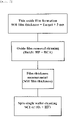
- FIG. 5 shows a simplified flowchart of a conventional method corresponding to the method disclosed in Patent Document 3.
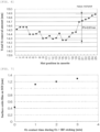
- This method can improve the uniformity of the SOI film thickness by reducing a peak to valley (PV) value of the SOI film thickness variations, which, for example, occur within a batch (twenty five wafers) as shown in FIG. 6 .
- PV peak to valley
- the SOI film thickness adjustment using a single wafer cleaning device can correct the SOI film thickness variations within the batch, it cannot provide a large etching removal amount because in-plane variations will increase depending on the removal amount, which is due to facts such as that the temperature of a chemical liquid is relatively high at a chemical liquid application section and that the centrifugal force created by rotation of a wafer holding section causes the flow velocity of the chemical liquid to be faster around the periphery of the wafer.
- Patent Document 3 proposes a method of controlling an in-batch average of the SOI film thickness after the batch cleaning to be a value between the target value and the target value + 0.5 nm in order to minimize the deterioration of the film thickness uniformity caused by the single wafer cleaning machine.
- Patent Document 4 discloses thinning the SOI film using ozone water and HF during final adjustment of the SOI film thickness.
- the flowchart shown in FIG. 5 also corresponds to the method disclosed in Patent Document 4.
- the etching in this method is one in which a surface oxide film formed by ozone water is removed with HF, so that the etching removal amount is controlled by the thickness of the surface oxide film formed by ozone water.
- the growth rate of the surface oxide film formed by ozone water depends on the thickness of the surface oxide film; when the surface oxide film is thin, the oxidation rate is high, and when, for example, the surface oxide film exceeds 1 nm as shown in FIG. 7 , the oxidation rate becomes extremely low and almost no growth occurs.
- the Si etching is saturated at about 0.5 nm ( FIG. 8 ).
- etching of about 0.5 nm or more by treatment with ozone water and HF takes too much time.
- the treatment with ozone water and HF needs to be repeated.
- the film thickness that can be etched by this repetition corresponds to the thickness of the oxide film saturated by ozone water, which means that the etching is performed in units of this thickness (equivalent to 0.5 nm Si thickness).
- An object of the present invention is to provide a method for manufacturing an SOI wafer that allows for both controlling the etching removal amount and achieving excellent in-plane uniformity of the SOI film thickness in adjusting the SOI film thickness of the SOI wafer.
- the present invention provides a method for manufacturing an SOI wafer comprising a step of performing an adjustment to a film thickness of an SOI layer of the SOI wafer by wet etching,
- the inventive method for manufacturing an SOI wafer performs a first etching step where an SC1 solution is used and a second etching step where an oxide film is formed by using ozone water and the oxide film is removed by using an HF-containing aqueous solution, wherein the first and second etching steps are performed in combination during the step of performing an adjustment to the film thickness of the SOI layer. Additionally, the first and second etching steps are performed such that a removal amount of the SOI layer in the first etching step is smaller than that in the second etching step.
- This feature allows for precisely controlling any etching removal amount while inhibiting deterioration of the in-plane film thickness uniformity.
- the inventive method for manufacturing an SOI wafer allows for both controlling the etching removal amount and achieving excellent in-plane uniformity of the SOI film thickness in adjusting the SOI film thickness of the SOI wafer.
- the removal amount of the SOI layer in the first etching step is preferably 0.5 nm or less.
- the second etching step can be repeated a plurality of times.
- the high-precision first etching step can be combined with the second etching step, which performs step-by-step etching in units of 0.5 nm, allowing for selection of a target value after the film thinning from a wider range of values.
- the first etching step and the second etching step are preferably performed using a single wafer spin etching machine.
- Using a single wafer spin etching machine allows for control according to the film thickness of each wafer, which makes it possible to control the film thickness with greater precision. Additionally, using a single wafer spin etching machine easily allows for repeating the second etching step using the ozone water and the HF-containing aqueous solution any number of times.
- the SOI layer to be subjected to the adjustment of the film thickness preferably has a film thickness of 50 nm or less.
- the present invention is suitable for thinning the SOI layer having an extremely thin film thickness of 50 nm or less.
- the present invention can manufacture an SOI wafer with a thinned film closer to a target value.
- the film thickness of the SOI layer to be subjected to the film thickness adjustment is, for example, 5 nm or more, though there is no particular lower limit on the film thickness.
- the second etching step is performed a plurality of times, and the removal amount of the SOI layer in the first etching step is 1 nm or less.
- the inventive method for manufacturing an SOI wafer allows for both controlling the etching removal amount and achieving excellent in-plane uniformity of the SOI film thickness in adjusting the SOI film thickness of the SOI wafer.
- the inventive method for manufacturing an SOI wafer allows for precisely controlling the SOI film thickness to a target value while achieving excellent in-plane uniformity of the film thickness of the extremely thin SOI film.
- a first etching step and a second etching step are performed in combination, where an SC1 solution is used in the first etching step and, in the second etching step, an oxide film is formed by using ozone water and then the oxide film is removed by using an HF-containing aqueous solution, and further the first and second etching steps are performed such that a removal amount of the SOI layer in the first etching step is smaller than that in the second etching step.
- the present invention is a method for manufacturing an SOI wafer comprising a step of performing an adjustment to a film thickness of an SOI layer of the SOI wafer by wet etching,
- the inventive method for manufacturing an SOI wafer performs, in the step of performing an adjustment to the film thickness of the SOI layer, a first etching step where an SC1 solution is used and a second etching step (which may be hereinafter referred to as "etching with O 3 + HF") where an oxide film is formed by using ozone water and then the oxide film is removed by using an HF-containing aqueous solution, wherein the first and second etching steps are performed in combination . Additionally, the etchings in the first etching step and the second etching step are performed such that a removal amount of the SOI layer in the first etching step is smaller than a removal amount of the SOI layer in the second etching step.
- FIG. 1 shows etching time dependence of an etching removal amount (in-plane average) when an SOI film is etched with an SC1 solution using a single wafer etching machine (spin etching machine), i.e., time dependence of the etching amount of SOI layer using the SC1 solution.
- the etching removal amount (in-plane average) using the SC1 solution is proportional to the etching time. Accordingly, in the first etching step, the etching removal amount (in-plane average) can be set to any value by adjusting the etching time.
- an in-plane removal amount Range (in-plane difference between maximum and minimum values of the etching removal amount) tends to deteriorate as the etching removal amount (in-plane average) using the SC1 solution increases.
- the present invention has a feature in that the etching with O 3 + HF (the second etching step) is employed in combination with the first etching step, in which the SC1 solution is used, to adjust the SOI film thickness.
- FIG. 2 shows relationship between the etching removal amount (in-plane average) and the in-plane removal amount Range when one cycle of the etching with O 3 + HF is performed (shown by the white circle) and then the first etching step with the SC1 solution is performed (shown by the white triangles).
- the in-plane removal amount Range can be restricted by performing the etching such that the target etching removal amount minus the removal amount in the second etching step, i.e., the removal amount of the SOI layer in the first etching step, is smaller than the removal amount of the SOI layer in the second etching step.
- the inventive method for manufacturing an SOI wafer allows for both controlling the etching removal amount and achieving excellent in-plane uniformity of the SOI film thickness in adjusting the SOI film thickness of the SOI wafer.
- the inventive method for manufacturing an SOI wafer allows for precisely controlling the SOI film thickness to a target value while achieving excellent in-plane uniformity of the SOI film thickness.
- the removal amount of the SOI layer in the first etching step is preferably 0.5 nm or less.
- the removal amount of the SOI layer in the first etching step can be, for example, 0.05 nm or more, though there is no particular lower limit on the removal amount.
- the second etching step can be performed a plurality of times.
- the high-precision first etching step can be combined with the second etching step, which performs step-by-step etching in units of 0.5 nm, allowing for selection of a target value after the film thinning from a wider range of values.
- the first etching step with the SC1 solution can be performed with the etching removal amount of 0.5 nm or less, and the remaining thickness can be etched through repetitions of the second etching step with the ozone water and the HF-containing aqueous solution.
- the treatment is performed during a period in which the surface oxide film formed by ozone water is saturated (about 1 min), and repeating the treatment enables the etching in units of 0.5 nm.
- the second etching step is performed a plurality of times and the removal amount of the SOI layer in the first etching step is 1 nm or less.
- the removal amount of the SOI layer is about 0.5 nm, so that the removal amount of the SOI layer in the first etching step needs to be 0. 5 nm or less.
- the removal amount of the SOI layer is at least about 1 nm. Accordingly, by setting the removal amount of the SOI layer in the first etching step to 1 nm or less, the removal amount of the SOI layer in the first etching step can be less than half of the total removal amount, which allows for achieving more excellent in-plane uniformity of the SOI film thickness.
- the order of the first etching step with the SC1 solution and the second etching step with the ozone water and the HF-containing aqueous solution is not limited to a particular order; performing the second etching step before, after, or both before and after the first etching step with the SC1 solution can provide the same effects.
- the second etching step may be performed a plurality of times after the first etching step, or may be performed a plurality of times before the first etching step. Alternatively, the second etching step may be performed one or more times before the first etching step and one or more times after the first etching step.
- treatment with the ozone water may be added as a final step to hydrophilize the surface.
- cleaning with the ozone water or the SC1 solution may be added to remove LPD.
- Performing the first etching step (etching with the SC1 solution) and the second etching step (etching with the ozone water and the HF-containing aqueous solution) in a single wafer spin etching machine allows for control according to the film thickness of each wafer, which makes it possible to control the film thickness with greater precision. Also, the etching with O 3 + HF can be easily repeated any number of times.
- FIG. 3 is a schematic illustration showing an example single wafer spin etching machine.
- the single wafer spin etching machine 10 shown in FIG. 3 includes a wafer holding and rotating mechanism 1 and a supply nozzle 2.
- the wafer holding and rotating mechanism 1 is configured to hold and rotate an SOI wafer 20 including an SOI layer to be subjected to the film thickness adjustment.
- the supply nozzle 2 is configured to supply a chemical liquid 3 for use in each etching step onto the wafer 20.
- the etching machine that can be used in the inventive method for manufacturing an SOI wafer is not limited to a particular machine, and any machine that is configured to adjust the SOI film thickness of the SOI wafer can be used.
- a single wafer cleaning machine can be used as the single wafer etching machine.
- the method for thinning an SOI wafer described above can be applied to any SOI wafer preparation method, including an ion implantation separation method, a SIMOX method, and an rT-CCP method.
- SC1 solution used in the first etching step use can be made of a mixed aqueous solution of NH 4 OH and H 2 O 2 , which is commonly used as an SC1 solution for cleaning of silicon wafers in semiconductor manufacturing.
- ozone water for the second etching step use can be made of ozone water having an ozone (O 3 ) concentration of 1 to 50 ppm.
- the HF-containing aqueous solution used in the second etching step can have an HF concentration in the range of 0.1 wt % to 50 wt %.
- an SOI wafer to be subjected to the treatment is provided (S1).
- S1 an SOI wafer to be subjected to the treatment.
- the provided SOI wafer is subjected to thin oxide film formation (S2).
- the oxide film is formed under conditions such that the SOI film thickness is about 3 nm thicker than a target value (Target).
- oxide film removal cleaning is performed to remove the oxide film formed on the surface of the SOI layer (S3).
- the oxide film is removed using an HF-containing aqueous solution, followed by RCA cleaning.
- the SOI film thickness with the oxide film removed is measured (S4).
- S4 the SOI film thickness with the oxide film removed.
- an ellipsometer can be used for the measurement.
- the step of adjusting the film thickness of the SOI layer of the SOI wafer is performed by wet etching (S5).
- the film thickness of the SOI layer is adjusted by single wafer spin etching.
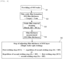
- FIG. 4 shows two examples in the step of adjusting the SOI film thickness, namely an example where the first etching step using the SC1 solution is performed and then the second etching step with O 3 + HF is performed a plurality of times, and an example where the second etching step with O 3 + HF is performed a plurality of times and then the first etching step using the SC1 solution is performed, eventually followed by the second etching step with O 3 + HF.
- the total removal amount in the first etching step is made smaller than the total removal amount in the second etching step.
- the provided twenty-five wafers were subjected to an oxidation step under the conditions shown in Table 1 below.
- Each wafer having the SOI film thickness measured after the oxidation step was subjected to oxidation film removal cleaning with an HF-containing aqueous solution in a batch cleaning machine. The conditions are shown in Table 2 below. Then, each wafer was subjected to SOI film thickness measurement. The results are shown in Table 2 below.
- each wafer was subjected to the etching with the SC1 solution (the first etching step) and then to the etching with O 3 + HF (bringing the wafer into contact with the ozone water, followed by etching it with the HF-containing aqueous solution (the second etching step)).
- the etching with the SC1 solution was performed so as to adjust the film thickness with the removal amount of 0. 5 nm or less, as shown in Table 2 below.
- the etching with O 3 + HF was performed repeatedly, as shown in Table 2 below. The number of repetitions was varied depending on the film thickness value of each wafer. In the repetitions of the etching with O 3 +HF, treatment with the ozone water was added as a final step to hydrophilize the surface. The SOI wafers were thus manufactured.
- Comparative Example 1 SOI wafers were manufactured in the same manner as in Example 1, except that SC1 etching was performed under the conditions shown in Table 2 below after the oxide film removal cleaning in batch cleaning and that the second etching step was not performed during the film thickness adjustment etching in the single wafer process. That is, in Comparative Example 1, the film thickness adjustment etching was performed only by the SC1 cleaning (etching with the SC1 solution).
- Comparative Example 2 SOI wafers were manufactured in the same manner as in Example 1, except that the film thickness adjustment etching was performed only by the etching with O 3 + HF (the second etching step).
- the conditions of the second etching step performed in Comparative Example 2 are shown in Table 2 below.
- Ozone water O 3 (12 ppm).
- HF HF-containing aqueous solution
- Example 2 on the other hand, as is apparent from the results shown in Table 2, the in-batch average of SOI film thickness within the same cassette was precisely adjusted to the target (target value) of 12.0 nm, and the average Range within the cassette also greatly improved to 0.2 nm. Also, the in-plane Range was 0.6 nm, which was better than Comparative Example 1.
Landscapes
- Weting (AREA)
- Chemical & Material Sciences (AREA)
- Chemical Kinetics & Catalysis (AREA)
- General Chemical & Material Sciences (AREA)
- Cleaning Or Drying Semiconductors (AREA)
Abstract
Description
- The present invention relates to a method for manufacturing an SOI wafer.
- SOI wafers, in particular those called FDSOI (fully depleted silicon-on-insulator) wafers, are required to have extremely high uniformity of film thickness of an SOI layer (SOI film thickness).
- Conventionally, as one method for thinning an SOI wafer, the method has been performed in which SOI wafer is subjected to heat treatment in a batch heat treatment furnace to change Si on the surface of the SOI layer into an oxide film by oxidation and then the oxide film is removed. In order to precisely reduce the SOI film thickness to an intended value in this method, it is required to accurately control the thickness of the oxide film to a target value. However, it is very difficult to accurately control the thickness of an actual oxide film, which is grown by heat treatment, because the oxidation rate varies with fluctuations in atmospheric pressure during oxidation. Thus, the following method has been employed when performing film thinning by oxidation: film thinning by oxidation is performed such that the SOI film thickness after the film thinning is slightly (about 3 nm) thicker than an intended value, and then, separately, an etching period is controlled so that the intended value is achieved by film thinning by etching. As disclosed in
Patent Document 1, this two-step film thinning method has been performed such that the oxide film after the oxidation is removed and then the SOI film thickness is measured to set a removal amount in the subsequent etching step based on the measured value. - There is also proposed a method to shorten the steps in the above two-step film thinning process including oxidation and etching; the method measures the SOI film thickness with the oxide film remaining after the oxidation and, based on the measured value of the SOI film thickness, performs oxide film removal, etching, and cleaning steps in the same batch cleaning process.
Patent Document 2 proposes etching with an SC1 solution as an etchant for use in this method. -
Patent Document 3 proposes a method to improve uniformity of the SOI film thickness in the following manner; during etching of an SOI wafer after oxidation, the method adjusts the film thickness to be slightly thicker than a target film thickness by batch cleaning, and then in order to adjust variations in the SOI film thickness within the batch, the method further performs final adjustment of the film thickness to the target value by means of single wafer SC1 etching or the like, based on an etching removal amount for each wafer.FIG. 5 shows a simplified flowchart of a conventional method corresponding to the method disclosed inPatent Document 3. This method can improve the uniformity of the SOI film thickness by reducing a peak to valley (PV) value of the SOI film thickness variations, which, for example, occur within a batch (twenty five wafers) as shown inFIG. 6 . However, although the SOI film thickness adjustment using a single wafer cleaning device can correct the SOI film thickness variations within the batch, it cannot provide a large etching removal amount because in-plane variations will increase depending on the removal amount, which is due to facts such as that the temperature of a chemical liquid is relatively high at a chemical liquid application section and that the centrifugal force created by rotation of a wafer holding section causes the flow velocity of the chemical liquid to be faster around the periphery of the wafer. Thus, for such a method,Patent Document 3 proposes a method of controlling an in-batch average of the SOI film thickness after the batch cleaning to be a value between the target value and the target value + 0.5 nm in order to minimize the deterioration of the film thickness uniformity caused by the single wafer cleaning machine. - Meanwhile,
Patent Document 4 discloses thinning the SOI film using ozone water and HF during final adjustment of the SOI film thickness. The flowchart shown inFIG. 5 also corresponds to the method disclosed inPatent Document 4. The etching in this method is one in which a surface oxide film formed by ozone water is removed with HF, so that the etching removal amount is controlled by the thickness of the surface oxide film formed by ozone water. However, the growth rate of the surface oxide film formed by ozone water depends on the thickness of the surface oxide film; when the surface oxide film is thin, the oxidation rate is high, and when, for example, the surface oxide film exceeds 1 nm as shown inFIG. 7 , the oxidation rate becomes extremely low and almost no growth occurs. As such, the Si etching is saturated at about 0.5 nm (FIG. 8 ). - Therefore, etching of about 0.5 nm or more by treatment with ozone water and HF, though it provides high in-plane uniformity of the etching removal amount, takes too much time. Thus, the treatment with ozone water and HF needs to be repeated. The film thickness that can be etched by this repetition corresponds to the thickness of the oxide film saturated by ozone water, which means that the etching is performed in units of this thickness (equivalent to 0.5 nm Si thickness). Also, even when etching in an amount at or below the saturation of the thickness of the surface oxide film formed by ozone water (about 0.5 nm or less) is performed for final film thickness adjustment, it is difficult to precisely control the etching removal amount because immersion-time dependent changes in the thickness of the surface oxide film formed by ozone water will be large.
-
- Patent Document 1:
JP 2007-266059 A - Patent Document 2:
JP 2010-092909 A - Patent Document 3:
JP 2016-004890 A - Patent Document 4:
JP 2004-349493 A - The present invention has been made to solve the above problems. An object of the present invention is to provide a method for manufacturing an SOI wafer that allows for both controlling the etching removal amount and achieving excellent in-plane uniformity of the SOI film thickness in adjusting the SOI film thickness of the SOI wafer.
- To achieve the object, the present invention provides a method for manufacturing an SOI wafer comprising a step of performing an adjustment to a film thickness of an SOI layer of the SOI wafer by wet etching,
- wherein in the step of performing the adjustment to the film thickness of the SOI layer:
- a first etching step of etching a surface of the SOI layer using an SC1 solution; and
- a second etching step of etching the surface of the SOI layer by bringing the SOI layer into contact with ozone water to form an oxide film on the surface of the SOI layer and then bringing the formed oxide film into contact with an HF-containing aqueous solution to remove the oxide film,
- the etchings in the first etching step and the second etching step are performed such that a removal amount of the SOI layer in the first etching step is smaller than a removal amount of the SOI layer in the second etching step.
- As described above, the inventive method for manufacturing an SOI wafer performs a first etching step where an SC1 solution is used and a second etching step where an oxide film is formed by using ozone water and the oxide film is removed by using an HF-containing aqueous solution, wherein the first and second etching steps are performed in combination during the step of performing an adjustment to the film thickness of the SOI layer. Additionally, the first and second etching steps are performed such that a removal amount of the SOI layer in the first etching step is smaller than that in the second etching step. This feature allows for precisely controlling any etching removal amount while inhibiting deterioration of the in-plane film thickness uniformity. In other words, the inventive method for manufacturing an SOI wafer allows for both controlling the etching removal amount and achieving excellent in-plane uniformity of the SOI film thickness in adjusting the SOI film thickness of the SOI wafer.
- The removal amount of the SOI layer in the first etching step is preferably 0.5 nm or less.
- With this feature, more excellent in-plane uniformity of the SOI film thickness can be achieved.
- The second etching step can be repeated a plurality of times.
- With this feature, the high-precision first etching step can be combined with the second etching step, which performs step-by-step etching in units of 0.5 nm, allowing for selection of a target value after the film thinning from a wider range of values.
- The first etching step and the second etching step are preferably performed using a single wafer spin etching machine.
- Using a single wafer spin etching machine allows for control according to the film thickness of each wafer, which makes it possible to control the film thickness with greater precision. Additionally, using a single wafer spin etching machine easily allows for repeating the second etching step using the ozone water and the HF-containing aqueous solution any number of times.
- The SOI layer to be subjected to the adjustment of the film thickness preferably has a film thickness of 50 nm or less.
- The present invention is suitable for thinning the SOI layer having an extremely thin film thickness of 50 nm or less. The present invention can manufacture an SOI wafer with a thinned film closer to a target value.
- The film thickness of the SOI layer to be subjected to the film thickness adjustment is, for example, 5 nm or more, though there is no particular lower limit on the film thickness.
- It is preferably that the second etching step is performed a plurality of times, and the removal amount of the SOI layer in the first etching step is 1 nm or less.
- With this feature, more excellent in-plane uniformity of the SOI film thickness can be achieved.
- As described above, the inventive method for manufacturing an SOI wafer allows for both controlling the etching removal amount and achieving excellent in-plane uniformity of the SOI film thickness in adjusting the SOI film thickness of the SOI wafer. As a result, the inventive method for manufacturing an SOI wafer allows for precisely controlling the SOI film thickness to a target value while achieving excellent in-plane uniformity of the film thickness of the extremely thin SOI film.
-
-
FIG. 1 is a graph showing time dependence of an etching removal amount of an SOI layer using an SC1 solution; -
FIG. 2 is a graph showing dependence of an in-plane removal amount Range on the etching removal amount, for each etchant used in a single wafer spin etching machine; -
FIG. 3 is a schematic illustration showing an example single wafer spin etching machine; -
FIG. 4 is a flowchart of an example of the inventive method for manufacturing an SOI wafer; -
FIG. 5 is a simplified flowchart of a conventional method; -
FIG. 6 is a graph showing an example of a variation in film thickness within a batch in batch cleaning; -
FIG. 7 is a graph showing relationship between ozone water contact time and thickness of a surface oxide film on the SOI in a conventional method; and -
FIG. 8 is a graph showing relationship between ozone water contact time and an etching removal amount of the SOI layer in the conventional method. - As noted above, there have been demands for development of a method for manufacturing an SOI wafer that allows for both controlling the etching removal amount and achieving excellent in-plane uniformity of the SOI film thickness in adjusting the SOI film thickness of the SOI wafer.
- The present inventors have earnestly studied to achieve the above object and consequently found that it is possible to precisely control any etching removal amount while inhibiting deterioration of in-plane film thickness uniformity through the following technique: in a step of performing an adjustment to a film thickness of the SOI layer, a first etching step and a second etching step are performed in combination, where an SC1 solution is used in the first etching step and, in the second etching step, an oxide film is formed by using ozone water and then the oxide film is removed by using an HF-containing aqueous solution, and further the first and second etching steps are performed such that a removal amount of the SOI layer in the first etching step is smaller than that in the second etching step. This finding has led to the completion of the present invention.
- Specifically, the present invention is a method for manufacturing an SOI wafer comprising a step of performing an adjustment to a film thickness of an SOI layer of the SOI wafer by wet etching,
- wherein in the step of performing the adjustment to the film thickness of the SOI layer:
- a first etching step of etching a surface of the SOI layer using an SC1 solution; and
- a second etching step of etching the surface of the SOI layer by bringing the SOI layer into contact with ozone water to form an oxide film on the surface of the SOI layer and then bringing the formed oxide film into contact with an HF-containing aqueous solution to remove the oxide film,
- the etchings in the first etching step and the second etching step are performed such that a removal amount of the SOI layer in the first etching step is smaller than a removal amount of the SOI layer in the second etching step.
- Hereinafter, the present invention will be described in detail with reference to the drawings, but the present invention is not limited thereto.
- As described above, the inventive method for manufacturing an SOI wafer performs, in the step of performing an adjustment to the film thickness of the SOI layer, a first etching step where an SC1 solution is used and a second etching step (which may be hereinafter referred to as "etching with O3 + HF") where an oxide film is formed by using ozone water and then the oxide film is removed by using an HF-containing aqueous solution, wherein the first and second etching steps are performed in combination . Additionally, the etchings in the first etching step and the second etching step are performed such that a removal amount of the SOI layer in the first etching step is smaller than a removal amount of the SOI layer in the second etching step.
-
FIG. 1 shows etching time dependence of an etching removal amount (in-plane average) when an SOI film is etched with an SC1 solution using a single wafer etching machine (spin etching machine), i.e., time dependence of the etching amount of SOI layer using the SC1 solution. - As shown in
FIG. 1 , the etching removal amount (in-plane average) using the SC1 solution is proportional to the etching time. Accordingly, in the first etching step, the etching removal amount (in-plane average) can be set to any value by adjusting the etching time. - On the other hand, as shown by the black circles in
FIG. 2 , an in-plane removal amount Range (in-plane difference between maximum and minimum values of the etching removal amount) tends to deteriorate as the etching removal amount (in-plane average) using the SC1 solution increases. - Thus, the present invention has a feature in that the etching with O3 + HF (the second etching step) is employed in combination with the first etching step, in which the SC1 solution is used, to adjust the SOI film thickness.
- The example of
FIG. 2 (white circle and white triangles) shows relationship between the etching removal amount (in-plane average) and the in-plane removal amount Range when one cycle of the etching with O3 + HF is performed (shown by the white circle) and then the first etching step with the SC1 solution is performed (shown by the white triangles). - It can also be seen from
FIG. 2 that, with a target etching removal amount set to 1 nm, performing the etching with the SC1 solution alone results in the in-plane removal amount Range of about 0.45 nm, but employing the etching with O3 + HF (the second etching step) and the etching with the SC1 solution (the first etching step) in combination can restrict the in-plane removal amount Range to about 0.25 nm. - It can also be seen from
FIG. 2 that the in-plane removal amount Range can be restricted by performing the etching such that the target etching removal amount minus the removal amount in the second etching step, i.e., the removal amount of the SOI layer in the first etching step, is smaller than the removal amount of the SOI layer in the second etching step. - Therefore, the inventive method for manufacturing an SOI wafer allows for both controlling the etching removal amount and achieving excellent in-plane uniformity of the SOI film thickness in adjusting the SOI film thickness of the SOI wafer. As a result, the inventive method for manufacturing an SOI wafer allows for precisely controlling the SOI film thickness to a target value while achieving excellent in-plane uniformity of the SOI film thickness.
- The removal amount of the SOI layer in the first etching step is preferably 0.5 nm or less.
- With this feature, more excellent in-plane uniformity of the SOI film thickness can be achieved.
- The removal amount of the SOI layer in the first etching step can be, for example, 0.05 nm or more, though there is no particular lower limit on the removal amount.
- Additionally, the second etching step can be performed a plurality of times.
- With this feature, the high-precision first etching step can be combined with the second etching step, which performs step-by-step etching in units of 0.5 nm, allowing for selection of a target value after the film thinning from a wider range of values.
- For example, in adjusting the film thickness of the SOI wafer, the first etching step with the SC1 solution can be performed with the etching removal amount of 0.5 nm or less, and the remaining thickness can be etched through repetitions of the second etching step with the ozone water and the HF-containing aqueous solution. Also, in the second etching step with the ozone water and the HF-containing aqueous solution, the treatment is performed during a period in which the surface oxide film formed by ozone water is saturated (about 1 min), and repeating the treatment enables the etching in units of 0.5 nm. The combination of the repetitions of the second etching step of 0. 5 nm with the ozone water and the HF-containing aqueous solution and the first etching solution of 0.5 nm or less with the SC1 solution makes it possible to both precisely control any etching removal amount and achieve more excellent uniformity of the in-plane film thickness.
- Alternatively, it is also preferred that the second etching step is performed a plurality of times and the removal amount of the SOI layer in the first etching step is 1 nm or less.
- When the second etching step is performed only once, the removal amount of the SOI layer is about 0.5 nm, so that the removal amount of the SOI layer in the first etching step needs to be 0. 5 nm or less. However, when the second etching step is performed a plurality of times, the removal amount of the SOI layer is at least about 1 nm. Accordingly, by setting the removal amount of the SOI layer in the first etching step to 1 nm or less, the removal amount of the SOI layer in the first etching step can be less than half of the total removal amount, which allows for achieving more excellent in-plane uniformity of the SOI film thickness.
- The order of the first etching step with the SC1 solution and the second etching step with the ozone water and the HF-containing aqueous solution is not limited to a particular order; performing the second etching step before, after, or both before and after the first etching step with the SC1 solution can provide the same effects.
- When the second etching step is performed a plurality of times, the second etching step may be performed a plurality of times after the first etching step, or may be performed a plurality of times before the first etching step. Alternatively, the second etching step may be performed one or more times before the first etching step and one or more times after the first etching step.
- In repeating the second etching step, treatment with the ozone water may be added as a final step to hydrophilize the surface.
- After the removal of the oxide film with the HF-containing aqueous solution in the second etching step, cleaning with the ozone water or the SC1 solution may be added to remove LPD.
- Performing the first etching step (etching with the SC1 solution) and the second etching step (etching with the ozone water and the HF-containing aqueous solution) in a single wafer spin etching machine allows for control according to the film thickness of each wafer, which makes it possible to control the film thickness with greater precision. Also, the etching with O3 + HF can be easily repeated any number of times.
- An example single wafer spin etching machine that can be used in the inventive method for manufacturing an SOI wafer is now described.
-
FIG. 3 is a schematic illustration showing an example single wafer spin etching machine. The single waferspin etching machine 10 shown inFIG. 3 includes a wafer holding androtating mechanism 1 and asupply nozzle 2. The wafer holding androtating mechanism 1 is configured to hold and rotate anSOI wafer 20 including an SOI layer to be subjected to the film thickness adjustment. Thesupply nozzle 2 is configured to supply achemical liquid 3 for use in each etching step onto thewafer 20. - Should be noted that the etching machine that can be used in the inventive method for manufacturing an SOI wafer is not limited to a particular machine, and any machine that is configured to adjust the SOI film thickness of the SOI wafer can be used. Thus, for example, a single wafer cleaning machine can be used as the single wafer etching machine.
- The method for thinning an SOI wafer described above can be applied to any SOI wafer preparation method, including an ion implantation separation method, a SIMOX method, and an rT-CCP method.
- As the SC1 solution used in the first etching step, use can be made of a mixed aqueous solution of NH4OH and H2O2, which is commonly used as an SC1 solution for cleaning of silicon wafers in semiconductor manufacturing.
- As the ozone water for the second etching step, use can be made of ozone water having an ozone (O3) concentration of 1 to 50 ppm.
- The HF-containing aqueous solution used in the second etching step can have an HF concentration in the range of 0.1 wt % to 50 wt %.
- A specific example of the inventive method for manufacturing an SOI wafer is now described with reference to
FIG. 4 . - First, an SOI wafer to be subjected to the treatment is provided (S1). As mentioned earlier, there are no particular limitations on methods for manufacturing the SOI wafer in the present invention.
- Then, the provided SOI wafer is subjected to thin oxide film formation (S2). In this example, the oxide film is formed under conditions such that the SOI film thickness is about 3 nm thicker than a target value (Target).
- Then, oxide film removal cleaning is performed to remove the oxide film formed on the surface of the SOI layer (S3). In this example, in a batch treatment process, the oxide film is removed using an HF-containing aqueous solution, followed by RCA cleaning.
- Then, the SOI film thickness with the oxide film removed is measured (S4). For example, an ellipsometer can be used for the measurement.
- Then, the step of adjusting the film thickness of the SOI layer of the SOI wafer is performed by wet etching (S5). In this example, the film thickness of the SOI layer is adjusted by single wafer spin etching.
-
FIG. 4 shows two examples in the step of adjusting the SOI film thickness, namely an example where the first etching step using the SC1 solution is performed and then the second etching step with O3 + HF is performed a plurality of times, and an example where the second etching step with O3 + HF is performed a plurality of times and then the first etching step using the SC1 solution is performed, eventually followed by the second etching step with O3 + HF. In either example, the total removal amount in the first etching step is made smaller than the total removal amount in the second etching step. - The present invention is described below in detail using Example and Comparative Examples, although the present invention is not limited thereto.
- Twenty-five SOI wafers with a diameter of 300 mm and an SOI film thickness of 150 nm fabricated by an ion implantation separation method were provided.
- The provided twenty-five wafers were subjected to an oxidation step under the conditions shown in Table 1 below.
- Each wafer subjected to the oxidation step was subjected to oxide film/SOI film thickness measurement. The results are shown in Table 1 below.
- Each wafer having the SOI film thickness measured after the oxidation step was subjected to oxidation film removal cleaning with an HF-containing aqueous solution in a batch cleaning machine. The conditions are shown in Table 2 below. Then, each wafer was subjected to SOI film thickness measurement. The results are shown in Table 2 below.
- Subsequently, using a single wafer etching machine (spin etching machine), each wafer was subjected to the etching with the SC1 solution (the first etching step) and then to the etching with O3 + HF (bringing the wafer into contact with the ozone water, followed by etching it with the HF-containing aqueous solution (the second etching step)). The etching with the SC1 solution was performed so as to adjust the film thickness with the removal amount of 0. 5 nm or less, as shown in Table 2 below. The etching with O3 + HF was performed repeatedly, as shown in Table 2 below. The number of repetitions was varied depending on the film thickness value of each wafer. In the repetitions of the etching with O3+HF, treatment with the ozone water was added as a final step to hydrophilize the surface. The SOI wafers were thus manufactured.
- After the second etching step, the SOI film thickness of each SOI wafer was measured. The results are shown in Table 2 below.
- In Comparative Example 1, SOI wafers were manufactured in the same manner as in Example 1, except that SC1 etching was performed under the conditions shown in Table 2 below after the oxide film removal cleaning in batch cleaning and that the second etching step was not performed during the film thickness adjustment etching in the single wafer process. That is, in Comparative Example 1, the film thickness adjustment etching was performed only by the SC1 cleaning (etching with the SC1 solution).
- In Comparative Example 2, SOI wafers were manufactured in the same manner as in Example 1, except that the film thickness adjustment etching was performed only by the etching with O3 + HF (the second etching step). The conditions of the second etching step performed in Comparative Example 2 are shown in Table 2 below.
- The results of each SOI film thickness measurement in Comparative Examples 1 and 2 are shown in Table 2 below, along with the results of Example 1.
[Table 1] Comparative Examples 1 and 2 and Example (in common) SOI film thickness of provided SOI wafers (before film thinning) (Target value after film thinning: 12 nm) SOI film thickness = 150 nm Number of wafers provided: 25 wafers each Oxidation step (Oxidation conditions) 950°C, 2 hrs, under pyrogenic atmosphere Measurement of Oxide film/SOI film thickness (Ellipsometer) Oxide film thickness = 300 nm In-batch average of SOI film thickness = 15.8 nm (which represents, based on an SOI film thickness average calculated for each wafer (measured at 41 points in the plane), an average of the averages of 25 wafers.) In-batch average Range = 1.2 nm (which represents, based on an SOI film thickness average calculated for each wafer, a Range (maximum value - minimum value) of the averages within the batch (25 wafers).) In-plane Range = 0.5 nm (which represents, based on an in-plane Range (maximum value - minimum value) calculated for each wafer, an average of the Ranges of 25 wafers.) [Table 2] Comparative Example 1 Comparative Example 2 Example 1 Batch cleaning Oxide film removal cleaning (HF) HF 15%, 100 sec HF 15%, 100 sec HF 15%, 100 sec SC1 etching SC1 120 sec (Average removal amount 3.4 nm) Not performed Not performed SOI film thickness measurement (Ellipsometer) In-Batch average of SOI film thickness = 12.4 nm In-Batch average of SOI film thickness = 15.8 nm In-Batch average of SOI film thickness = 15.8 nm [Single wafer film thickness adjustment etching] (1) SC1 etching (First etching step) SC1 20-60 sec (Removal amount: 0.3-0.5 nm) Not performed SC1 20-60 sec (Removal amount: 0.3-0.5 nm) (2) O3+HF etching (Second etching step) Not performed O3(1 min)+HF (repeated 7-9 times) (Removal amount: 3.5-4.5 nm) O3(1 min)+HF (repeated 6-8 times) (Removal amount: 3.0-4.0 nm) O3 surface finish Not performed Performed Performed SOI film thickness measurement (Ellipsometer) In-Batch average of SOI film thickness = 12.0 nm In-Batch average of SOI film thickness = 11.8 nm In-Batch average of SOI film thickness = 12.0 nm Batch average Range = 0.2 nm Batch average Range = 0.9 nm Batch average Range = 0.2 nm In-plane Range = 0.9 nm In-plane Range = 0.5 nm In-plane Range = 0.6 nm - SC1 conditions: NH4OH (29 wt%): H2O2 (30 wt%): H2O = 1:1:5, liquid temperature of 76°.
- Ozone water: O3 (12 ppm).
- HF (HF-containing aqueous solution) in the second etching step: HF (15 wt%).
- In the case of Comparative Example 1, where the film thickness was adjusted only with the SC1 solution, the in-batch average of SOI film thickness and the in-batch average Range within the same cassette were as good as 12.0 nm and 0.2 nm, respectively, but the average of the in-plane Ranges of the respective wafers was detrimentally increased to 0.9 nm due to deterioration of the in-plane film thickness distribution of each wafer, which was caused by the SC1 cleaning.
- In the case of Comparative Example 2, where the film thickness was adjusted only with the ozone water and HF, the in-plane Range was as good as 0.5 nm, but the in-batch average of SOI film thickness within the same cassette was 11.8 nm, which was off from the target. Additionally, the batch average Range was 0.9 nm, showing no substantial improvement.
- In Example, on the other hand, as is apparent from the results shown in Table 2, the in-batch average of SOI film thickness within the same cassette was precisely adjusted to the target (target value) of 12.0 nm, and the average Range within the cassette also greatly improved to 0.2 nm. Also, the in-plane Range was 0.6 nm, which was better than Comparative Example 1.
- It should be noted that the present invention is not limited to the above-described embodiments. The embodiments are just examples, and any examples that substantially have the same feature and demonstrate the same functions and effects as those in the technical concept disclosed in claims of the present invention are included in the technical scope of the present invention.
Claims (6)
- A method for manufacturing an SOI wafer comprising a step of performing an adjustment to a film thickness of an SOI layer of the SOI wafer by wet etching,wherein in the step of performing the adjustment to the film thickness of the SOI layer:a first etching step of etching a surface of the SOI layer using an SC1 solution; anda second etching step of etching the surface of the SOI layer by bringing the SOI layer into contact with ozone water to form an oxide film on the surface of the SOI layer and then bringing the formed oxide film into contact with an HF-containing aqueous solution to remove the oxide film,are performed in combination, andthe etchings in the first etching step and the second etching step are performed such that a removal amount of the SOI layer in the first etching step is smaller than a removal amount of the SOI layer in the second etching step.
- The method for manufacturing an SOI wafer according to claim 1, wherein the removal amount of the SOI layer in the first etching step is 0.5 nm or less.
- The method for manufacturing an SOI wafer according to claim 1 or 2, wherein the second etching step is repeated a plurality of times.
- The method for manufacturing an SOI wafer according to any one of claims 1 to 3, wherein the first etching step and the second etching step are performed using a single wafer spin etching machine.
- The method for manufacturing an SOI wafer according to any one of claims 1 to 4, wherein the SOI layer to be subjected to the adjustment of the film thickness has a film thickness of 50 nm or less.
- The method for manufacturing an SOI wafer according to claim 1, wherein the second etching step is performed a plurality of times, and the removal amount of the SOI layer in the first etching step is 1 nm or less.
Applications Claiming Priority (2)
| Application Number | Priority Date | Filing Date | Title |
|---|---|---|---|
| JP2020091413 | 2020-05-26 | ||
| PCT/JP2021/015378 WO2021241044A1 (en) | 2020-05-26 | 2021-04-14 | Method for manufacturing soi wafer |
Publications (2)
| Publication Number | Publication Date |
|---|---|
| EP4160658A1 true EP4160658A1 (en) | 2023-04-05 |
| EP4160658A4 EP4160658A4 (en) | 2024-07-10 |
Family
ID=78744309
Family Applications (1)
| Application Number | Title | Priority Date | Filing Date |
|---|---|---|---|
| EP21812925.2A Pending EP4160658A4 (en) | 2020-05-26 | 2021-04-14 | Method for manufacturing soi wafer |
Country Status (7)
| Country | Link |
|---|---|
| US (1) | US12604688B2 (en) |
| EP (1) | EP4160658A4 (en) |
| JP (1) | JP7364071B2 (en) |
| KR (1) | KR20230014690A (en) |
| CN (1) | CN115516608B (en) |
| TW (1) | TWI893106B (en) |
| WO (1) | WO2021241044A1 (en) |
Family Cites Families (15)
| Publication number | Priority date | Publication date | Assignee | Title |
|---|---|---|---|---|
| JP3542376B2 (en) * | 1994-04-08 | 2004-07-14 | キヤノン株式会社 | Manufacturing method of semiconductor substrate |
| US7256104B2 (en) | 2003-05-21 | 2007-08-14 | Canon Kabushiki Kaisha | Substrate manufacturing method and substrate processing apparatus |
| JP2004349493A (en) | 2003-05-22 | 2004-12-09 | Canon Inc | Film thickness adjusting device and method of manufacturing SOI substrate |
| DE102004054566B4 (en) * | 2004-11-11 | 2008-04-30 | Siltronic Ag | Method and device for leveling a semiconductor wafer and semiconductor wafer with improved flatness |
| JP2006303089A (en) | 2005-04-19 | 2006-11-02 | Sumco Corp | Cleaning method of silicon substrate |
| JP2007266059A (en) | 2006-03-27 | 2007-10-11 | Sumco Corp | SIMOX wafer manufacturing method |
| WO2009123261A1 (en) * | 2008-04-01 | 2009-10-08 | 信越化学工業株式会社 | Method for producing soi substrate |
| JP5597915B2 (en) | 2008-08-12 | 2014-10-01 | 株式会社Sumco | Manufacturing method of bonded wafer |
| JP5320954B2 (en) | 2008-10-03 | 2013-10-23 | 信越半導体株式会社 | Manufacturing method of SOI wafer |
| JP5841306B2 (en) * | 2009-05-08 | 2016-01-13 | ルネサスエレクトロニクス株式会社 | Semiconductor device and manufacturing method thereof |
| JP5533624B2 (en) | 2010-12-16 | 2014-06-25 | 信越半導体株式会社 | Semiconductor wafer cleaning method |
| JP6152829B2 (en) | 2014-06-17 | 2017-06-28 | 信越半導体株式会社 | Manufacturing method of SOI wafer |
| US9735062B1 (en) * | 2016-06-03 | 2017-08-15 | International Business Machines Corporation | Defect reduction in channel silicon germanium on patterned silicon |
| JP6760245B2 (en) | 2017-11-06 | 2020-09-23 | 信越半導体株式会社 | Method for manufacturing an SOI wafer having a thin film SOI layer |
| FR3076070B1 (en) | 2017-12-22 | 2019-12-27 | Commissariat A L'energie Atomique Et Aux Energies Alternatives | METHOD FOR TRANSFERRING A USEFUL LAYER |
-
2021
- 2021-04-14 WO PCT/JP2021/015378 patent/WO2021241044A1/en not_active Ceased
- 2021-04-14 US US17/922,846 patent/US12604688B2/en active Active
- 2021-04-14 JP JP2022527564A patent/JP7364071B2/en active Active
- 2021-04-14 EP EP21812925.2A patent/EP4160658A4/en active Pending
- 2021-04-14 KR KR1020227039718A patent/KR20230014690A/en active Pending
- 2021-04-14 CN CN202180032683.7A patent/CN115516608B/en active Active
- 2021-04-22 TW TW110114438A patent/TWI893106B/en active
Also Published As
| Publication number | Publication date |
|---|---|
| WO2021241044A1 (en) | 2021-12-02 |
| TW202213493A (en) | 2022-04-01 |
| EP4160658A4 (en) | 2024-07-10 |
| JP7364071B2 (en) | 2023-10-18 |
| US12604688B2 (en) | 2026-04-14 |
| KR20230014690A (en) | 2023-01-30 |
| CN115516608A (en) | 2022-12-23 |
| CN115516608B (en) | 2025-08-01 |
| JPWO2021241044A1 (en) | 2021-12-02 |
| TWI893106B (en) | 2025-08-11 |
| US20230154761A1 (en) | 2023-05-18 |
Similar Documents
| Publication | Publication Date | Title |
|---|---|---|
| EP0676796A2 (en) | Semiconductor substrate and a method for manufacturing the same | |
| TWI640033B (en) | Method for manufacturing germanium wafer on insulator | |
| KR20230169118A (en) | Cleaning method of silicon wafer and manufacturing method of silicon wafer with natural oxide film attached | |
| US12604688B2 (en) | Method for manufacturing SOI wafer | |
| JP5458525B2 (en) | Manufacturing method of SOI wafer | |
| US6451660B1 (en) | Method of forming bipolar transistors comprising a native oxide layer formed on a substrate by rinsing the substrate in ozonated water | |
| TWI611568B (en) | Method for manufacturing germanium on insulator | |
| CN111403273B (en) | Wafer thinning process method | |
| JP3302228B2 (en) | Method for manufacturing SOI substrate | |
| JPH1116844A (en) | Manufacturing method of epitaxial silicon wafer and wafer for material | |
| JP2004349493A (en) | Film thickness adjusting device and method of manufacturing SOI substrate | |
| US20260005014A1 (en) | Method for oxidation of top silicon layer in bonded wafer | |
| JPS5927529A (en) | Fabrication of semiconductor device wafer | |
| JP7251419B2 (en) | Bonded SOI wafer manufacturing method | |
| CN121773751A (en) | Method for thinning surface layer of silicon-on-insulator substrate | |
| JP2026507741A (en) | Method for forming a weakened zone in a semiconductor substrate | |
| CN116936423A (en) | Epitaxial machine temperature correction method | |
| WO2025204274A1 (en) | Method for manufacturing epitaxial wafer | |
| CN114975228A (en) | Methods of fabricating semiconductor-on-insulator structures | |
| JPH0567626A (en) | Manufacture of semiconductor device | |
| JPS5944863A (en) | Manufacture of semiconductor integrated circuit | |
| JPS6286771A (en) | Method of manufacturing silicon diaphragm | |
| JPS6338234A (en) | Manufacture of substrate for semiconductor element | |
| JPS60208837A (en) | Taper etching method of thin film |
Legal Events
| Date | Code | Title | Description |
|---|---|---|---|
| STAA | Information on the status of an ep patent application or granted ep patent |
Free format text: STATUS: THE INTERNATIONAL PUBLICATION HAS BEEN MADE |
|
| PUAI | Public reference made under article 153(3) epc to a published international application that has entered the european phase |
Free format text: ORIGINAL CODE: 0009012 |
|
| STAA | Information on the status of an ep patent application or granted ep patent |
Free format text: STATUS: REQUEST FOR EXAMINATION WAS MADE |
|
| 17P | Request for examination filed |
Effective date: 20221108 |
|
| AK | Designated contracting states |
Kind code of ref document: A1 Designated state(s): AL AT BE BG CH CY CZ DE DK EE ES FI FR GB GR HR HU IE IS IT LI LT LU LV MC MK MT NL NO PL PT RO RS SE SI SK SM TR |
|
| DAV | Request for validation of the european patent (deleted) | ||
| DAX | Request for extension of the european patent (deleted) | ||
| A4 | Supplementary search report drawn up and despatched |
Effective date: 20240612 |
|
| RIC1 | Information provided on ipc code assigned before grant |
Ipc: H01L 21/762 20060101ALI20240606BHEP Ipc: H01L 27/12 20060101ALI20240606BHEP Ipc: H01L 21/02 20060101ALI20240606BHEP Ipc: H01L 21/306 20060101AFI20240606BHEP |