EP4159541A1 - Fahrzeugmontierte antriebsschaltung, fahrzeugmontierter antriebschip, fahrzeugmontierte antriebsvorrichtung und elektronische vorrichtung - Google Patents
Fahrzeugmontierte antriebsschaltung, fahrzeugmontierter antriebschip, fahrzeugmontierte antriebsvorrichtung und elektronische vorrichtung Download PDFInfo
- Publication number
- EP4159541A1 EP4159541A1 EP20940676.8A EP20940676A EP4159541A1 EP 4159541 A1 EP4159541 A1 EP 4159541A1 EP 20940676 A EP20940676 A EP 20940676A EP 4159541 A1 EP4159541 A1 EP 4159541A1
- Authority
- EP
- European Patent Office
- Prior art keywords
- circuit
- drive
- vehicle
- transistor
- fault
- Prior art date
- Legal status (The legal status is an assumption and is not a legal conclusion. Google has not performed a legal analysis and makes no representation as to the accuracy of the status listed.)
- Pending
Links
Images


Classifications
-
- H—ELECTRICITY
- H03—ELECTRONIC CIRCUITRY
- H03K—PULSE TECHNIQUE
- H03K17/00—Electronic switching or gating, i.e. not by contact-making and –breaking
- H03K17/06—Modifications for ensuring a fully conducting state
- H03K17/063—Modifications for ensuring a fully conducting state in field-effect transistor switches
-
- H—ELECTRICITY
- H03—ELECTRONIC CIRCUITRY
- H03K—PULSE TECHNIQUE
- H03K17/00—Electronic switching or gating, i.e. not by contact-making and –breaking
- H03K17/08—Modifications for protecting switching circuit against overcurrent or overvoltage
- H03K17/082—Modifications for protecting switching circuit against overcurrent or overvoltage by feedback from the output to the control circuit
-
- H—ELECTRICITY
- H03—ELECTRONIC CIRCUITRY
- H03K—PULSE TECHNIQUE
- H03K17/00—Electronic switching or gating, i.e. not by contact-making and –breaking
- H03K17/10—Modifications for increasing the maximum permissible switched voltage
-
- H—ELECTRICITY
- H03—ELECTRONIC CIRCUITRY
- H03K—PULSE TECHNIQUE
- H03K17/00—Electronic switching or gating, i.e. not by contact-making and –breaking
- H03K17/18—Modifications for indicating state of switch
-
- H—ELECTRICITY
- H03—ELECTRONIC CIRCUITRY
- H03K—PULSE TECHNIQUE
- H03K17/00—Electronic switching or gating, i.e. not by contact-making and –breaking
- H03K17/06—Modifications for ensuring a fully conducting state
- H03K2017/066—Maximizing the OFF-resistance instead of minimizing the ON-resistance
Definitions
- This application relates to the vehicle field, and in particular, to a vehicle-mounted drive circuit, a vehicle-mounted drive chip, a vehicle-mounted drive part, and an electronic device.
- a load in a vehicle needs to be driven by using a drive circuit.
- the load may include a motor, a dashboard, a speaker, a sensor, an electronic control unit (electronic control unit, ECU), a valve body, or the like.
- a drive circuit of the load usually includes a pre-drive circuit and a drive transistor (also referred to as a power transistor).
- the pre-drive circuit is connected to the drive transistor, and the drive transistor is further connected to each of a power supply and the load.
- the pre-drive circuit is configured to provide a switching signal for the drive transistor, to control the drive transistor to be conducted or cut off.
- a drive current may be provided for the load, to drive the load to operate; and when the drive transistor is cut off, the load stops operating.
- the pre-drive circuit may not be able to control a conducted/cutoff state of the drive transistor, resulting in a risk that a device in the drive circuit and the load are damaged.
- This application provides a vehicle-mounted drive circuit, a vehicle-mounted drive chip, a vehicle-mounted drive part, and an electronic device, to reduce a risk that an element in the drive circuit and a load are damaged when a drive transistor is faulty.
- this application provides a vehicle-mounted drive circuit.
- the vehicle-mounted drive circuit includes a drive chip, a first drive transistor, and a first switching transistor, and the drive chip includes a pre-drive circuit and a shut off circuit; the first drive transistor and the first switching transistor are connected in series, and the first drive transistor and the first switching transistor are connected in series between a power supply and a first load; the pre-drive circuit is connected to a gate electrode of the first drive transistor, and the pre-drive circuit controls, in response to a first power-on instruction, the first drive transistor to be conducted, and controls, in response to a first power-off instruction, the first drive transistor to be cut off; and the shut off circuit is connected to a gate electrode of the first switching transistor, and the shut off circuit controls, in response to the first power-on instruction, the first switching transistor to be conducted, and controls, in response to the first power-off instruction or a first fault signal, the first switching transistor to be cut off.
- shut off circuit in the drive chip can cut off the first switching transistor in response to the first fault signal, it may be ensured that a current channel between the power supply and the first load is cut off in a timely manner in a fault scenario, to avoid a case in which each element in the vehicle-mounted drive circuit and the first load are damaged when continuously operating in the fault scenario.
- both the pre-drive circuit for controlling the current channel to be conducted or cut off and the shut off circuit for providing a redundant shut off path for the current channel are integrated into the drive chip, to avoid increasing a volume and costs of the drive circuit, and improve a degree of integration of the vehicle-mounted drive circuit.
- the shut off circuit includes an interface sub-circuit and an execution sub-circuit, and the execution sub-circuit is connected to each of the interface sub-circuit and the gate electrode of the first switching transistor; the interface sub-circuit provides a first switching signal for the execution sub-circuit in response to the first power-on instruction, and provides a second switching signal for the execution sub-circuit in response to the first power-off instruction or the first fault signal; and the execution sub-circuit controls, in response to the first switching signal, the first switching transistor to be conducted, and controls, in response to the second switching signal, the first switching transistor to be cut off.
- the execution sub-circuit may be a push-pull circuit.
- the push-pull circuit is used to control a conducted/cutoff state of the first switching transistor, to ensure that a conduction current required by the first switching transistor can be provided, and ensure a switching rate of the first switching transistor.
- the first switching transistor is an N-type transistor
- the shut off circuit further includes a first charge pump (charge pump); the first charge pump is connected to each of a power supply terminal and the execution sub-circuit, and the first charge pump is configured to: increase a voltage from the power supply terminal and provide the voltage for the execution sub-circuit; and the execution sub-circuit is configured to control, under driving of the first charge pump and in response to the first switching signal, the first switching transistor to be conducted.
- charge pump charge pump
- the voltage from the power supply terminal is increased by using the first charge pump, to ensure that the execution sub-circuit can effectively conduct the first switching transistor.
- the first fault signal includes a first fault sub-signal
- the drive chip further includes a fault detection circuit connected to the shut off circuit; and the fault detection circuit is configured to detect whether the vehicle-mounted drive circuit is faulty, and the fault detection circuit sends the first fault sub-signal to the shut off circuit if the fault detection circuit detects that the vehicle-mounted drive circuit is faulty.
- the fault detection circuit integrated into the drive chip detects a fault, to ensure that the first fault sub-signal can be sent to the shut off circuit in a timely manner when the fault is detected, to indicate the shut off circuit to cut off the first switching transistor in a timely manner.
- the drive chip further includes one or more of a peripheral interface, a first current detection circuit, a watchdog circuit, and a temperature sensor;
- the peripheral interface is connected to a main control circuit, and the peripheral interface is configured to: communicate with the main control circuit, and send a first interrupt instruction to the fault detection circuit if detecting that communication with the main control circuit is interrupted;
- the watchdog circuit is connected to each of the peripheral interface and the fault detection circuit, and the watchdog circuit is configured to send a second interrupt instruction to the fault detection circuit if detecting that communication with the peripheral interface is interrupted;
- the first current detection circuit is connected to the fault detection circuit, and the first current detection circuit is configured to: detect a current in a first current channel between the power supply and the first load, and send, to the fault detection circuit, a first voltage for indicating a magnitude of the current in the first current channel;
- the temperature sensor is configured to: detect a junction temperature of the drive chip, and send the junction temperature to the fault detection circuit; and it is determined that the vehicle-mounted drive circuit is
- the fault detection circuit can detect a plurality of faults of different types, fault detection reliability is high.
- the drive chip includes the first current detection circuit
- the vehicle-mounted drive circuit further includes a first sampling resistor; the first sampling resistor is connected to the first drive transistor and the first switching transistor in series; and two input terminals of the first current detection circuit are bridged over two terminals of the first sampling resistor, a first output terminal of the first current detection circuit is connected to the fault detection circuit, and the first current detection circuit is configured to: collect a first voltage between the two terminals of the first sampling resistor, and send the collected first voltage to the fault detection circuit.
- the first voltage collected by the first current detection circuit may accurately reflect the magnitude of the current in the first current channel, so that the fault detection circuit can accurately determine whether the first current channel is short-circuited or open-circuited.
- a second output terminal of the first current detection circuit is connected to the peripheral interface; and the first current detection circuit is further configured to: perform analog-to-digital conversion on the collected voltage, to obtain a digital parameter of the voltage, and send the digital parameter to the main control circuit through the peripheral interface.
- the first current detection circuit sends the digital parameter of the collected voltage to the main control circuit, so that the main control circuit can also accurately determine, based on the voltage, whether the first current channel is short-circuited or open-circuited.
- the first current detection circuit includes a first filter, a second filter, a differential amplifier (differential amplifier), and an analog-to-digital converter (analog-to-digital converter, ADC); an input terminal of the first filter is connected to one terminal of the first sampling resistor, and an output terminal of the first filter is connected to a first input terminal of the differential amplifier; an input terminal of the second filter is connected to the other terminal of the first sampling resistor, and an output terminal of the second filter is connected to a second input terminal of the differential amplifier; and an output terminal of the differential amplifier is connected to each of the fault detection circuit and an input terminal of the analog-to-digital converter, and an output terminal of the analog-to-digital converter is connected to the peripheral interface.
- ADC analog-to-digital converter
- the two filters may be configured to filter out a high-frequency glitch on the voltage between the two terminals of the first sampling resistor, and the differential amplifier can amplify the collected voltage and provide the amplified voltage to each of the fault detection circuit and the analog-to-digital converter, so that a next circuit can accurately determine, based on the amplified voltage, whether the first current channel is short-circuited or open-circuited.
- a control terminal of the differential amplifier is further connected to the peripheral interface; and the peripheral interface is further configured to configure a gain of the differential amplifier in response to a gain configuration instruction sent by the main control circuit.
- the main control circuit may flexibly configure the gain of the differential amplifier, current collection flexibility and accuracy are effectively improved.
- the vehicle-mounted drive circuit further includes a second drive transistor, a second switching transistor, a second current detection circuit, and a second sampling resistor; the second drive transistor, the second switching transistor, and the second sampling resistor are connected in series, and the second drive transistor, the second switching transistor, and the second sampling resistor are connected in series between the power supply and a second load; the pre-drive circuit is further connected to a gate electrode of the second drive transistor, and the pre-drive circuit is further configured to: control, in response to a second power-on instruction, the second drive transistor to be conducted, and control, in response to a second power-off instruction, the second drive transistor to be cut off; the shut off circuit is further connected to the gate electrode of the second switching transistor, and the shut off circuit is further configured to: control, in response to the second power-on instruction, the second switching transistor to be conducted, and control, in response to the second power-off instruction or a second fault signal, the second switching transistor to be cut off; two input terminals of the second current detection circuit are bridged over two terminal
- the drive chip in the vehicle-mounted drive circuit provided in this embodiment of this application may control a conducted/cutoff state of at least two current channels, a degree of integration of the vehicle-mounted drive circuit is effectively improved, and a volume of the vehicle-mounted drive circuit is reduced.
- one current detection circuit is configured for each current channel, to independently detect a current in each current channel, and further independently control each current channel.
- the first fault signal includes a second fault sub-signal
- the shut off circuit is further connected to the main control circuit through the peripheral interface of the drive chip; and the peripheral interface is configured to: receive the second fault sub-signal sent by the main control circuit, and send, to the shut off circuit for sending, the second fault sub-signal sent by the main control circuit.
- the shut off circuit may further control, in response to the second fault sub-signal sent by the main control circuit, the first switching transistor to be cut off. Therefore, reliability of cutting off the first switching transistor in the fault scenario is effectively improved.
- the drive chip further includes a second charge pump; and the second charge pump is connected to the pre-drive circuit, and is configured to provide a drive voltage for the pre-drive circuit.
- the switching transistor and the drive transistor may be respectively driven by using two independent charge pumps, a case in which a supply fault is caused when a charge pump is shared can be avoided, to ensure drive reliability.
- the drive chip is further configured to control, in response to the first fault signal, the first drive transistor to be cut off. Therefore, it can be ensured that when one of the first drive transistor and the first switching transistor fails, the first current channel between the power supply and the first load may be cut off by cutting off another transistor, to ensure fault protection reliability.
- a vehicle-mounted drive chip includes a first drive transistor, a first switching transistor, a pre-drive circuit, and a shut off circuit; the first drive transistor and the first switching transistor are connected in series, and the first drive transistor and the first switching transistor are connected in series between a power supply and a first load; the pre-drive circuit is connected to a gate electrode of the first drive transistor, and the pre-drive circuit controls, in response to a first power-on instruction, the first drive transistor to be conducted, and controls, in response to a first power-off instruction, the first drive transistor to be cut off; and the shut off circuit is connected to a gate electrode of the first switching transistor, and the shut off circuit controls, in response to the first power-on instruction, the first switching transistor to be conducted, and controls, in response to the first power-off instruction or a first fault signal, the first switching transistor to be cut off.
- the shut off circuit in the drive chip can cut off the first switching transistor in response to the first fault signal, it may be ensured that a current channel between the power supply and the first load is cut off in a timely manner in a fault scenario, to avoid a case in which each element in the vehicle-mounted drive circuit and the first load are damaged when continuously operating in the fault scenario.
- the pre-drive circuit, the shut off circuit, the drive transistor, and the switching transistor are all integrated into the drive chip, to effectively improve a degree of integration of the drive circuit.
- a vehicle-mounted drive part includes a main control circuit and a drive circuit, and the drive circuit is the vehicle-mounted drive circuit or the vehicle-mounted drive chip provided in the foregoing aspects; the main control circuit is connected to the drive circuit, and is configured to: send a first power-on instruction to each of a pre-drive circuit and a shut off circuit in the drive circuit in response to a power-on request for a first load, and send a first power-off instruction to each of the pre-drive circuit and the shut off circuit in response to a power-off request for the first load.
- the main control circuit is further configured to: detect whether the vehicle-mounted drive part is faulty, and send a second fault sub-signal to the drive circuit if detecting that the vehicle-mounted drive part is faulty.
- an electronic device includes a power supply, a first load, and the vehicle-mounted drive part provided in the foregoing aspects; and a first drive transistor and a first switching transistor in the vehicle-mounted drive part are connected in series between the power supply and the first load.
- the vehicle-mounted drive circuit includes a drive chip, and a first drive transistor and a first switching transistor that are connected in series between a power supply and a first load
- the drive chip includes a pre-drive circuit and a shut off circuit. Because the shut off circuit can cut off the first switching transistor in response to the first fault signal, it may be ensured that a current channel between the power supply and the first load is cut off in a timely manner in the fault scenario, to avoid a case in which each element in the vehicle-mounted drive circuit and the first load are damaged when continuously operating in the fault scenario.
- both the shut off circuit and the pre-drive circuit are integrated into the drive chip, to avoid increasing a volume and costs of the vehicle-mounted drive circuit, and improve a degree of integration of the vehicle-mounted drive circuit.
- FIG. 1 is a schematic diagram of a structure of a vehicle-mounted drive circuit according to an embodiment of this application.
- a vehicle-mounted drive 10 circuit includes a drive chip 100, a first drive transistor M11, and a first switching transistor M12.
- the drive chip 100 includes a pre-drive circuit 101 and a shut off circuit 102.
- the first drive transistor M11 and the first switching transistor M12 are connected in series, and the first drive transistor M11 and the first switching transistor M12 are connected in series between a power supply 20 and a first load 30.
- a drain electrode of the first switching transistor M12 is connected to the power supply 20, a source electrode of the first switching transistor M12 is connected to a drain electrode of the first drive transistor M11, and a source electrode of the first drive transistor M11 is connected to the first load 30.
- a position of the first drive transistor M11 and a position of the first switching transistor M12 may be exchanged.
- the drain electrode of the first drive transistor M11 is connected to the power supply 20, and the source electrode of the first switching transistor M12 is connected to the first load 30.
- the first drive transistor M11 may also be referred to as a main power transistor.
- the pre-drive circuit 101 is connected to a gate electrode of the first drive transistor M11, and the pre-drive circuit 101 controls, in response to a first power-on instruction, the first drive transistor M11 to be conducted, and controls, in response to a first power-off instruction, the first drive transistor M11 to be cut off.
- the shut off circuit 102 is connected to a gate electrode of the first switching transistor M12, and the shut off circuit 102 controls, in response to the first power-on instruction, the first switching transistor M12 to be conducted, and controls, in response to the first power-off instruction or a first fault signal, the first switching transistor M12 to be cut off.
- a first current channel between the power supply 20 and the first load 30 is conducted, and the power supply 20 can provide a drive current for the first load 30 by using the first drive transistor M11 and the first switching transistor M12, to drive the first load 30 to operate.
- the first current channel between the power supply 20 and the first load 30 is cut off, the power supply 20 cannot provide the drive current for the first load 30, and the first load 30 stops operating.
- both the first power-on instruction and the first power-off instruction may be sent by a main control circuit.
- the main control circuit may send the first power-on instruction to each of the pre-drive circuit 101 and the shut off circuit 102, to conduct the first drive transistor M11 and the first switching transistor M12.
- the main control circuit may further send the first power-off instruction to each of the pre-drive circuit 101 and the shut off circuit 102, to cut off the first drive transistor M11 and the first switching transistor M12.
- the first fault signal may be sent after the main control circuit detects a fault, or may be generated after a fault detection circuit inside the drive chip 100 detects a fault.
- the main control circuit or the fault detection circuit sends the first fault signal to the shut off circuit 102, to indicate the shut off circuit 102 to cut off the first switching transistor M12, so that it can be ensured that the first current channel between the power supply 20 and the first load 30 is cut off in a timely manner, to effectively avoid spreading the fault and a disaster.
- the shut off circuit 102 can cut off the first switching transistor M12 in a timely manner in a fault scenario, the shut off circuit 102 may also be referred to as an emergency shut off (emergency shut off) circuit.
- the main control circuit or the fault detection circuit may send the first fault signal to the pre-drive circuit 101 after detecting the fault.
- the pre-drive circuit 101 may cut off the first drive transistor M11 in response to the first fault signal. Therefore, it can be ensured that when one of the first drive transistor M11 and the first switching transistor M12 fails, the first current channel between the power supply 20 and the first load 30 may be cut off by cutting off another transistor, to ensure fault protection reliability.
- this embodiment of this application provides a vehicle-mounted drive circuit.
- the vehicle-mounted drive circuit includes the drive chip, and the first drive transistor and the first switching transistor that are connected in series between the power supply and the first load. Because the shut off circuit in the drive chip can cut off the first switching transistor in response to the first fault signal, it may be ensured that the current channel between the power supply and the first load is cut off in a timely manner in the fault scenario, to avoid a case in which each element in the vehicle-mounted drive circuit and the first load are damaged when continuously operating in the fault scenario. Because the shut off circuit provides a redundant shut off path for the first current channel, reliability of the vehicle-mounted drive circuit during operation is effectively improved.
- both the pre-drive circuit for controlling the current channel to be conducted or cut off and the shut off circuit for providing the redundant shut off path for the current channel are integrated into the drive chip, to avoid increasing a volume and costs of the vehicle-mounted drive circuit, and improve a degree of integration of the vehicle-mounted drive circuit.
- both the first drive transistor and the first switching transistor are disposed independently of the drive chip and are not integrated into the drive chip, a problem that the drive chip is overheated due to a large drive current does not need to be considered. In other words, the first drive transistor and the first switching transistor may provide a large drive current for the first load.
- FIG. 2 is a schematic diagram of a structure of a shut off circuit according to an embodiment of this application.
- the vehicle-mounted drive circuit 10 further includes a power supply terminal V1 and a ground terminal V2.
- the power supply terminal V1 is connected to the power supply 20, and is configured to provide a drive voltage.
- the drive voltage may be 12 volts (V) or 24 V
- the shut off circuit 102 includes an interface sub-circuit 1021 and an execution sub-circuit 1022, and the execution sub-circuit 1022 is connected to each of the interface sub-circuit 1021, a gate electrode of the first switching transistor M12, the power supply terminal V1, and the ground terminal V2.
- the interface sub-circuit 1021 provides a first switching signal for the execution sub-circuit 1022 in response to the first power-on instruction, and provides a second switching signal for the execution sub-circuit 1022 in response to a cutoff instruction or the first fault signal.
- the interface sub-circuit 1021 may be configured to: receive an instruction, process the received instruction, and provide a switching signal for the execution sub-circuit 1022.
- the interface sub-circuit 1021 may include a transistor and a resistor.
- the execution sub-circuit 1022 controls, in response to the first switching signal and under driving of the power supply terminal V1, the first switching transistor M12 to be conducted, and controls, in response to the second switching signal, the first switching transistor M12 to be cut off.
- the execution sub-circuit 1022 may be a push-pull (push pull) circuit.
- the push-pull circuit includes two transistors T1 and T2 that are symmetrically disposed and have different polarities.
- the transistor T1 is a P-type transistor
- the transistor T2 is an N-type transistor.
- Gate electrodes of the two transistors T1 and T2 are both connected to the interface sub-circuit 1021, a source electrode of the transistor T1 is connected to the power supply terminal V1, a drain electrode is connected to the gate electrode of the first switching transistor M12, a source electrode of the transistor T2 is connected to the ground terminal V2, and a drain electrode is connected to the gate electrode of the first switching transistor M12.
- the execution sub-circuit 1022 may be an open drain (open drain, OD) circuit.
- the interface sub-circuit 1021 When the interface sub-circuit 1021 provides the first switching signal, the transistor T1 is conducted, the transistor T2 is cut off, and a voltage of the power supply terminal V1 is loaded onto the gate electrode of the first switching transistor M12, so that the first switching transistor M12 is conducted.
- the interface sub-circuit 1021 provides the second switching signal, the transistor T2 is conducted, the transistor T1 is cut off, and a voltage of the ground terminal V2 is loaded onto the gate electrode of the first switching transistor M12, so that the first switching transistor M12 is cut off.
- the push-pull circuit is used to control a conducted/cutoff state of the first switching transistor M12, to ensure that a conduction current required by the first switching transistor M12 can be provided, and ensure a switching rate of the first switching transistor M12.
- the first switching transistor M12 may be an N-type transistor.
- the shut off circuit 102 further includes a first charge pump 1023.
- the first charge pump 1023 is connected to each of the power supply terminal V1 and the execution sub-circuit 1022, and the first charge pump 1023 is configured to: increase the drive voltage provided by the power supply terminal V1 and provide the increased drive voltage for the execution sub-circuit 1022.
- the execution sub-circuit 1022 may control, in response to the first switching signal and under driving of the first charge pump 1023, the first switching transistor M12 to be conducted.
- the first charge pump 1023 needs to provide a high voltage for the gate electrode of the first switching transistor M12, to ensure that the first switching transistor M12 can be normally conducted.
- the first fault signal received by the shut off circuit 102 may include a first fault sub-signal.
- the drive chip 100 further includes a fault detection circuit 103 connected to the shut off circuit 102.
- the fault detection circuit 103 is configured to detect whether the vehicle-mounted drive circuit 10 is faulty.
- the fault detection circuit 103 sends the first fault sub-signal to the shut off circuit 102 if the fault detection circuit 103 detects that the vehicle-mounted drive circuit is faulty.
- the fault detection circuit 103 may also be referred to as a build in self test (build in self test, BIST) circuit.
- the fault detection circuit 103 integrated into the drive chip 100 detects a fault, to ensure that the first fault sub-signal can be sent to the shut off circuit 102 in a timely manner when the fault is detected, to indicate the shut off circuit 102 to cut off the first switching transistor M12 in a timely manner, so as to avoid a physical damage caused when the drive chip 100 and an external transistor are in an abnormal operating state for a long time period.
- the fault detection circuit 103 may control the shut off circuit 102 to cut off the first switching transistor M12 within 1 ms.
- the drive chip 100 may further include one or more of a peripheral interface 104, a first current detection circuit 105, a watchdog (watchdog) circuit 106, and a temperature sensor 107.
- the drive chip 100 shown in FIG. 3 includes the peripheral interface 104, the first current detection circuit 105, the watchdog circuit 106, and the temperature sensor 107.
- the peripheral interface 104 is connected to a main control circuit 40, and the peripheral interface 104 is configured to: communicate with the main control circuit 40, and send a first interrupt instruction to the fault detection circuit 103 if detecting that communication with the main control circuit 40 is interrupted.
- the peripheral interface 104 may be a serial peripheral interface (serial peripheral interface, SPI).
- the watchdog circuit 106 is connected to each of the peripheral interface 104 and the fault detection circuit 103, and the watchdog circuit 106 is configured to send a second interrupt instruction to the fault detection circuit 103 if detecting that communication with the peripheral interface 104 is interrupted (in other words, handshake communication is abnormal).
- the first current detection circuit 105 is connected to the fault detection circuit 103.
- the first current detection circuit 105 is configured to: detect a current in the first current channel between the power supply 20 and the first load 30, and send, to the fault detection circuit 103, a first voltage for indicating a magnitude of the current.
- the temperature sensor 107 is configured to: detect a junction temperature of the drive chip 100, and send the junction temperature to the fault detection circuit 103.
- the junction temperature is a temperature of a PN junction inside the drive chip 100, that is, a maximum temperature inside the drive chip.
- the fault detection circuit 103 prestores a first voltage threshold, a second voltage threshold, and a third voltage threshold, the first voltage threshold is greater than the third voltage threshold, and the third voltage threshold is greater than the second voltage threshold. If the fault detection circuit 103 detects, when the first current channel is conducted (in other words, after the first power-on instruction is received), that the first voltage sent by the first current detection circuit 105 is greater than the first voltage threshold, the fault detection circuit 103 may determine that the current in the first current channel is an overcurrent, and further, may determine that the first current channel is short-circuited to the ground.
- the fault detection circuit 103 may determine that the first current channel is short-circuited to the power supply. If the fault detection circuit 103 detects, when the first current channel is conducted, that the first voltage sent by the first current detection circuit 105 is less than the third voltage threshold, the fault detection circuit 103 may determine that the first current channel is open-circuited.
- a magnitude of a current indicated by the first voltage threshold is an upper limit value that is of the current in the first current channel and that exists when the vehicle-mounted drive circuit 10 operates normally and the first current channel between the power supply 20 and the first load 30 is conducted.
- a magnitude of a current indicated by the second voltage threshold is an upper limit value that is of the current in the first current channel and that exists when the vehicle-mounted drive circuit 10 operates normally and the first current channel between the power supply 20 and the first load 30 is cut off.
- a magnitude of a current indicated by the third voltage threshold is a lower limit value that is of the current in the first current channel and that exists when the vehicle-mounted drive circuit 10 operates normally and the first current channel between the power supply 20 and the first load 30 is conducted.
- the first current detection circuit 105 may directly collect and send a current value of the first current channel.
- the fault detection circuit 103 prestores a first current threshold, a second current threshold, and a third current threshold, the first current threshold is greater than the third current threshold, and the third current threshold is greater than the second current threshold. If the fault detection circuit 103 detects, when the first current channel is conducted, that the current value sent by the first current detection circuit 105 is greater than the first current threshold, the fault detection circuit 103 may determine that the first current channel is short-circuited to the ground.
- the fault detection circuit 103 may determine that the first current channel is short-circuited to the power supply. If the fault detection circuit 103 detects, when the first current channel is conducted, that the current value sent by the first current detection circuit 105 is less than the third current threshold, the fault detection circuit 103 may determine that the first current channel is open-circuited.
- the first current threshold is an upper limit value that is of the current in the first current channel and that exists when the vehicle-mounted drive circuit 10 operates normally and the first current channel between the power supply 20 and the first load 30 is conducted.
- the second current threshold is an upper limit value that is of the current in the first current channel and that exists when the vehicle-mounted drive circuit 10 operates normally and the first current channel between the power supply 20 and the first load 30 is cut off.
- the third current threshold is a lower limit value that is of the current in the first current channel and that exists when the vehicle-mounted drive circuit 10 operates normally and the first current channel between the power supply 20 and the first load 30 is conducted.
- the fault detection circuit 103 prestores the temperature threshold, and the temperature threshold is an upper limit value that is of the junction temperature and that exists when the drive chip 100 operates normally. If the fault detection circuit 103 detects that the junction temperature sent by the temperature sensor 107 is greater than the temperature threshold, the fault detection circuit 103 may determine that the drive chip 100 is overheated, and further, may determine that the vehicle-mounted drive circuit 10 is faulty.
- the fault detection circuit 103 can detect a plurality of faults of different types, fault detection reliability is high, and reliability of the vehicle-mounted drive circuit during operation is also high.
- the drive chip 100 includes the first current detection circuit 105, and the vehicle-mounted drive circuit 10 further includes a first sampling resistor R1.
- the first sampling resistor R1 is connected to the first drive transistor M11 and the first switching transistor M12 in series.
- one terminal of the first sampling resistor R1 is connected to the source electrode of the first drive transistor M11, and the other terminal is connected to the first load 30.
- the first sampling resistor R1 may alternatively be connected in series between the first drive transistor M11 and the first switching transistor M12, or connected in series between the power supply 20 and the first switching transistor M12.
- Two input terminals of the first current detection circuit 105 are bridged over two terminals of the first sampling resistor R1, a first output terminal of the first current detection circuit 105 is connected to the fault detection circuit 103, and the first current detection circuit 105 is configured to: collect a first voltage between the two terminals of the first sampling resistor R1, and send the collected first voltage to the fault detection circuit 103.
- the fault detection circuit 103 may accurately determine, based on a magnitude of the voltage, whether the first current channel between the power supply 20 and the first load 30 is short-circuited or open-circuited.
- a second output terminal of the first current detection circuit 105 is further connected to the peripheral interface 104.
- the first current detection circuit 105 is further configured to: perform analog-to-digital conversion on the collected voltage, to obtain a digital parameter of the voltage, and send the digital parameter to the main control circuit 40 through the peripheral interface 104.
- the main control circuit 40 may further determine, based on the magnitude of the voltage, whether the first current channel between the power supply 20 and the first load 30 is short-circuited or open-circuited. Further, the main control circuit 40 may send a fault signal (for example, a second fault sub-signal) to the shut off circuit 102 when detecting that the first current channel is short-circuited or open-circuited, to ensure reliability of cutting off the first current channel.
- a fault signal for example, a second fault sub-signal
- the first current detection circuit 105 may include a first filter F1, a second filter F2, a differential amplifier 1051, and an analog-to-digital converter 1052.
- An input terminal of the first filter F1 is connected to one terminal of the first sampling resistor R1, and an output terminal of the first filter F1 is connected to a first input terminal of the differential amplifier 1051.
- An input terminal of the second filter F2 is connected to the other terminal of the first sampling resistor R1, and an output terminal of the second filter F2 is connected to a second input terminal of the differential amplifier 1051.
- An output terminal of the differential amplifier 1051 is connected to each of the fault detection circuit 103 and an input terminal of the analog-to-digital converter 1052, and an output terminal of the analog-to-digital converter 1052 is connected to the peripheral interface 104.
- the first filter F1 and the second filter F2 each may be an electromagnetic interference (electromagnetic interference, EMI) filter.
- the EMI filter can filter out a high-frequency glitch on the voltage between the two terminals of the first sampling resistor R1, and can protect a voltage loaded at an input terminal of a next differential amplifier 1051 from being greater than a rated voltage (for example, 40 V or 45 V), to ensure that the differential amplifier 1051 operates normally.
- the differential amplifier 1051 is configured to: amplify the collected voltage, and provide the amplified voltage to each of the fault detection circuit 103 and the analog-to-digital converter 1052, so that a next circuit can accurately determine, based on the amplified voltage, whether the first current channel is short-circuited or open-circuited.
- the analog-to-digital converter 1052 is configured to: perform analog-to-digital conversion on the amplified voltage, to obtain a digital parameter of the voltage, and send the digital parameter to the main control circuit 40 through the peripheral interface 104.
- the main control circuit 40 may determine, based on the digital parameter, whether the first current channel is short-circuited or open-circuited.
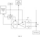
- FIG. 4 is a schematic diagram of a partial structure of a vehicle-mounted drive circuit according to an embodiment of this application.
- a control terminal of this differential amplifier 1051 is further connected to the peripheral interface 104.
- the peripheral interface 104 is further configured to configure a gain of the differential amplifier 1051 in response to a gain configuration instruction sent by the main control circuit 40.
- the gain configuration instruction sent by the main control circuit 40 may carry an initial gain represented by using an 8-bit (bit) binary number.
- the peripheral interface 104 may multiply the initial gain by a prestored target multiple, to obtain a target gain, and further, the gain of the differential amplifier 1051 may be set to the target gain.
- a developer may determine the target gain of the differential amplifier 1051 based on a range that is of the current in the first current channel and that exists when the first load 30 normally operates and a resistance value of the first sampling resistor R1.
- the developer may configure the main control circuit 40 based on the determined target gain, so that the main control circuit 40 can configure the gain of the differential amplifier 1051 through the peripheral interface 104 of the drive chip 100 when the vehicle-mounted drive circuit 10 is initialized. Because the main control circuit can flexibly configure the gain of the differential amplifier 1051 based on the range of the current in the first current channel and the resistance value of the first sampling resistor R1, current collection flexibility and accuracy are effectively improved.
- the driver chip 100 further includes a regulator 108.
- the regulator 108 may be a low dropout regulator (low dropout regulator, LDO).
- the regulator 108 is connected to each of the peripheral interface 104, the analog-to-digital converter 1052, and a drive power supply terminal VDD.
- the peripheral interface 104 may be further configured to configure a reference voltage of the analog-to-digital converter 1052 in response to a reference voltage configuration instruction sent by the main control circuit 40.
- the peripheral interface 104 may send, to the regulator 108, a target reference voltage carried in the reference voltage configuration instruction, and further, the regulator 108 may regulate a voltage of the drive power supply terminal VDD to the target reference voltage and provide the target reference voltage for the analog-to-digital converter 1052.
- the target reference voltage may be 2.5 V, 3.3 V, or 5 V
- a sampling rate of the analog-to-digital converter 1052 may be greater than or equal to 300 kilohertz (kHz), a resolution may be 12 bits, and an error is ⁇ 5 least significant bits (least significant bit, LSB).
- the main control circuit 40 configures a reference voltage of the analog-to-digital converter 1052 through the peripheral interface 104, to improve flexibility and reliability of the analog-to-digital converter 1052 during operation.
- the fault detection circuit 103 may detect a fault. If detection succeeds (in other words, no fault is detected), a notification message indicating that detection succeeds may be sent to the main control circuit 40 through the peripheral interface 104. After receiving the notification message, the main control circuit 40 may configure the reference voltage of the analog-to-digital converter 1052 through the peripheral interface 104, and sets an enabling flag bit of the analog-to-digital converter 1052 (in other words, the analog-to-digital converter 1052 is enabled). Then, the analog-to-digital converter 1052 may start to operate, and a corresponding register may be refreshed in real time by using a latest voltage collection result, so that the main control circuit 40 can read the latest voltage collection result in real time.
- the shut off circuit 102 is further connected to the main control circuit 40 through the peripheral interface 104 of the drive chip 100.
- the first fault signal received by the shut off circuit 102 may further include the second fault sub-signal sent by the main control circuit 40.
- the peripheral interface 104 is further configured to: receive the second fault sub-signal sent by the main control circuit 40, and send the second fault sub-signal to the shut off circuit 102.
- the shut off circuit 102 not only may control, in response to the first fault sub-signal sent by the fault detection circuit 103, the first switching transistor M12 to be cut off, but also may control, in response to the second fault sub-signal sent by the main control circuit 40, the first switching transistor M12 to be cut off. Therefore, reliability of cutting off the first switching transistor M12 in a fault scenario is effectively improved.
- FIG. 5 is a schematic diagram of a structure of still another vehicle-mounted drive circuit according to an embodiment of this application.
- the vehicle-mounted drive circuit may further include a second drive transistor M21, a second switching transistor M22, a second current detection circuit 108, and a second sampling resistor R2.
- the second drive transistor M21, the second switching transistor M22, and the second sampling resistor R2 are connected in series, and the second drive transistor M21, the second switching transistor M22, and the second sampling resistor R2 are connected in series between this power supply 20 and a second load 50.
- the pre-drive circuit 101 is further connected to a gate electrode of the second drive transistor M21, and the pre-drive circuit 101 is further configured to: control, in response to a second power-on instruction, the second drive transistor M21 to be conducted, and control, in response to a second power-off instruction, the second drive transistor M21 to be cut off.
- the shut off circuit 102 is further connected to a gate electrode of the second switching transistor M22, and the shut off circuit 102 is further configured to: control, in response to the second power-on instruction, the second switching transistor M22 to be conducted, and control, in response to the second power-off instruction or a second fault signal, the second switching transistor M22 to be cut off.
- both the second power-on instruction and the second power-off instruction may be sent by a main control circuit 40.
- the main control circuit 40 may send the second power-on instruction to each of the pre-drive circuit 101 and the shut off circuit 102, to conduct the second drive transistor M21 and the second switching transistor M22.
- the main control circuit 40 may further send the second power-off instruction to each of the pre-drive circuit 101 and the shut off circuit 102, to cut off the second drive transistor M21 and the second switching transistor M22.
- the second fault signal may be sent after the main control circuit 40 detects a fault, or may be sent after the fault detection circuit 103 detects a fault.
- the main control circuit 40 or the fault detection circuit 103 sends the second fault signal to the shut off circuit 102, to indicate the shut off circuit 102 to cut off the second switching transistor M22, so as to ensure that a second current channel between the power supply 20 and the second load 50 may be cut off in a timely manner, and avoid a case in which each element in the vehicle-mounted drive circuit 10 and the second load 50 are damaged when continuously operating in the fault scenario.
- Two input terminals of the second current detection circuit 108 are bridged over two terminals of the second sampling resistor R2, a first output terminal of the second current detection circuit 108 is connected to the fault detection circuit 103, and the second current detection circuit 108 is configured to: collect a second voltage between the two terminals of the second sampling resistor R2, and send the collected second voltage to the fault detection circuit 103.
- the second voltage indicates a magnitude of a current in the second current channel between the power supply 20 and the second load 50.
- the second fault signal is sent to the shut off circuit 102 if the fault detection circuit 103 detects any of the following cases:
- the first interrupt instruction is received.
- the second interrupt instruction is received.
- That the second current channel is short-circuited or open-circuited is determined based on the second voltage.
- the junction temperature is greater than the temperature threshold.
- the fault detection circuit 103 may send the first fault sub-signal and the second fault signal to the shut off circuit 102, to indicate the shut off circuit 102 to cut off both the first switching transistor M12 and the second switching transistor M22. However, if the fault detection circuit 103 detects that only the first current channel is short-circuited or open-circuited, the fault detection circuit 103 may send only the first fault sub-signal to the shut off circuit 102, to cut off the first switching transistor M12, and does not need to cut off the second switching transistor M22.
- the second switching transistor M22 may remain in a conducted state.
- the fault detection circuit 103 may indicate the shut off circuit 102 to cut off only the second switching transistor M22, and the first switching transistor M12 may remain in a conducted state.
- the drive chip in the vehicle-mounted drive circuit provided in this embodiment of this application may control a conducted/cutoff state of the two current channels, a degree of integration of the vehicle-mounted drive circuit is effectively improved, and a volume of the vehicle-mounted drive circuit is reduced.
- the vehicle-mounted drive circuit 10 may include a plurality of second drive transistors M21, a plurality of second switching transistors M22, a plurality of second current detection circuits 108, and a plurality of second sampling resistors R2.
- the vehicle-mounted drive circuit 10 may simultaneously drive a plurality of second loads 50.
- the vehicle-mounted drive circuit 10 may also be referred to as a multi-channel drive circuit, and the drive chip 100 in the vehicle-mounted drive circuit 10 may also be referred to as a multi-channel drive chip.
- the pre-drive circuit 101 may be referred to as a multi-channel pre-drive circuit
- the shut off circuit 102 may be referred to as a multi-channel shut off circuit.
- the vehicle-mounted drive circuit 10 can simultaneously drive eight loads.
- the drive chip 100 may be an 8-channel drive chip.
- a multi-channel drive chip 100 provided in this embodiment of this application may communicate with the main control circuit 40 through one peripheral interface 104, to effectively reduce a quantity of interfaces that need to be disposed in the main control circuit 40, so as to effectively simplify a circuit structure of the main control circuit 40 and reduce costs of the main control circuit 40.
- one current detection circuit is configured for each current channel, to independently detect a current in each current channel, and further independently control a conducted/cutoff state of each current channel. Therefore, flexibility of controlling each current channel in a multi-channel scenario is effectively improved.
- both a structure and an operating principle of the second current detection circuit 108 may be the same as those of the first current detection circuit 105. Details are not described herein again.
- FIG. 5 shows only a part of a connection relationship of the second current detection circuit 108.
- the current detection circuit is integrated into the drive chip 100, so that the vehicle-mounted drive circuit 10 can complete current collection by configuring only one sampling resistor for each current channel. This greatly simplifies a circuit design and reduces costs of the vehicle-mounted drive circuit.
- a resistance value of each sampling resistor used in the vehicle-mounted drive circuit 10 may be in a unit of milliohm.
- the resistance value of the sampling resistor may range from 0.1 milliohms to 50 milliohms.
- the second switching transistor M22 is also an N-type transistor.
- the first drive transistor M11 and the second drive transistor M21 each are also an N-type transistor.
- each transistor in the vehicle-mounted drive circuit 10 may be an N-channel enhanced metal-oxide-semiconductor field-effect transistor (metal-oxide-semiconductor field-effect transistor, MOSFET).
- MOSFET metal-oxide-semiconductor field-effect transistor
- a transistor in the vehicle-mounted drive circuit 10 may be an N-type insulated gate bipolar transistor (insulated gate bipolar transistor, IGBT).
- the drive chip 100 further includes a second charge pump 109.
- the second charge pump 109 is connected to the pre-drive circuit 101, and is configured to provide a drive voltage for the pre-drive circuit 101.
- the switching transistor and the drive transistor may be respectively driven by using two charge pumps, a case in which a pump pressure of a charge pump is faulty when the charge pump is shared can be avoided, to ensure drive reliability.
- the drive chip 100 may further include an input/output interface 110, a power supply circuit 111, and a channel diagnostor (channel diagnostics) 112.
- the input/output interface 110 is connected to each of the main control circuit 40 and the pre-drive circuit 101, to implement communication between the main control circuit 40 and the pre-drive circuit 101.
- the input/output interface 110 may be a general-purpose input/output (general-purpose input/output, GPIO) interface.
- the input/output interface 110 may be further connected to the shut off circuit 102.
- the main control circuit 40 may further communicate with the shut off circuit 102 through the input/output interface 110, for example, send a fault signal to the shut off circuit 102 through the input/output interface 110.
- the power supply circuit 111 is connected to each of the power supply 20 and another component in the drive chip 100, and is configured to supply power to each component in the drive chip 100.
- the channel diagnostor 112 is connected to each of the peripheral interface 104, the pre-drive circuit 101, and the fault detection circuit 103.
- the main control circuit 40 may send, to the channel diagnostor 112 through the peripheral interface 104, an identifier of a current channel that needs to be conducted currently.
- the channel diagnostor 112 may further determine, based on the pre-drive circuit 101, whether an actually conducted current channel is the same as the circuit channel indicated by the identifier sent by the main control circuit 40. If the actually conducted current channel is different from the circuit channel indicated by the identifier sent by the main control circuit 40, the channel diagnostor 112 may send a channel fault indication to the fault detection circuit 103, to indicate the fault detection circuit 103 to cut off the wrongly conducted current channel.
- this embodiment of this application provides a vehicle-mounted drive circuit.
- the vehicle-mounted drive circuit includes the drive chip, and the first drive transistor and the first switching transistor that are connected in series between the power supply and the first load. Because the shut off circuit in the drive chip can cut off the first switching transistor in response to the first fault signal, it may be ensured that the current channel between the power supply and the first load is cut off in a timely manner in the fault scenario, to avoid a case in which each element in the vehicle-mounted drive circuit and the first load are damaged when continuously operating in the fault scenario. Because the shut off circuit provides a redundant shut off path for the first current channel, reliability of the vehicle-mounted drive circuit during operation is effectively improved.
- both the pre-drive circuit for controlling the current channel to be conducted or cut off and the shut off circuit for providing the redundant shut off path for the current channel are integrated into the drive chip, to avoid increasing a volume and costs of the vehicle-mounted drive circuit, and improve a degree of integration of the vehicle-mounted drive circuit.
- both the first drive transistor and the first switching transistor are disposed independently of the drive chip and are not integrated into the drive chip, a problem that the drive chip is overheated due to a large drive current does not need to be considered. In other words, the first drive transistor and the first switching transistor may provide a large drive current for the first load.
- An embodiment of this application further provides a vehicle-mounted drive chip.
- the vehicle-mounted drive chip includes a first drive transistor M11, a first switching transistor M12, a pre-drive circuit 101, and a shut off circuit 102.
- the first drive transistor M11 and the first switching transistor M12 are connected in series, and the first drive transistor M11 and the first switching transistor M12 are connected in series between a power supply 20 and a first load 30.
- the pre-drive circuit 101 is connected to a gate electrode of the first drive transistor M11, and the pre-drive circuit 101 controls, in response to a first power-on instruction, the first drive transistor M11 to be conducted, and controls, in response to a first power-off instruction, the first drive transistor M11 to be cut off.
- the shut off circuit 102 is connected to a gate electrode of the first switching transistor M12, and the shut off circuit 102 controls, in response to the first power-on instruction, the first switching transistor M12 to be conducted, and controls, in response to the first power-off instruction or a first fault signal, the first switching transistor M12 to be cut off.
- the vehicle-mounted drive chip integrates both the first drive transistor M11 and the first switching transistor M12 into the chip, to further improve a degree of integration of the drive circuit and reduce a volume of the drive circuit.
- the vehicle-mounted drive chip may be a multi-channel drive chip. In other words, one or more second drive transistors and one or more second switching transistors may be integrated into the vehicle-mounted drive chip.
- the vehicle-mounted drive part includes a drive circuit 10 and a main control circuit 40.
- the drive circuit 10 is a vehicle-mounted drive circuit provided in the foregoing embodiment, for example, may be the vehicle-mounted drive circuit shown in FIG. 1 , FIG. 3 , or FIG. 5 .
- the drive circuit 10 is the vehicle-mounted drive chip provided in the foregoing embodiment, for example, may be the vehicle-mounted drive chip shown in FIG. 6 .
- the main control circuit 40 is connected to the drive circuit 10, and is configured to: send a first power-on instruction to each of a pre-drive circuit 101 and a shut off circuit 102 in the drive circuit 10 in response to a power-on request for a first load 30, and send a first power-off instruction to each of the pre-drive circuit 101 and the shut off circuit 102 in response to a power-off request for the first load 30.
- the main control circuit 40 may be a micro control unit (micro controller unit, MCU), or may be referred to as a single-chip microcomputer.
- MCU microcontrol unit
- the main control circuit 40 may be further configured to: detect whether the vehicle-mounted drive part is faulty, and send a second fault sub-signal to a peripheral interface 104 of the drive circuit 10 if detecting that the vehicle-mounted drive part is faulty.
- the second fault sub-signal is used to indicate the shut off circuit 102 in the drive circuit 10 to cut off a first switching transistor M12, in other words, to cut off a first current channel between a power supply 20 and the first load 30.
- the drive circuit 10 may be a multi-channel drive circuit.
- the main control circuit 40 may alternatively send a second fault signal to the peripheral interface 104, to indicate the shut off circuit 102 to cut off a second switching transistor M22, in other words, to cut off a second current channel between the power supply 20 and a second load 50.
- the vehicle-mounted drive part provided in this embodiment of this application may include a voltage collection circuit connected to the main control circuit 40, and the voltage collection circuit is further configured to be connected to the power supply 20.
- the voltage collection circuit can collect a voltage of the power supply 20 and send the voltage to the main control circuit 40.
- the main control circuit 40 may detect, based on the voltage collected by the voltage collection circuit, whether the power supply 20 is undervoltage or overvoltage. If detecting that the power supply 20 is undervoltage or overvoltage, the main control circuit 40 may send a second fault sub-signal and the second fault signal to the peripheral interface 104.
- the vehicle-mounted drive part may be applied to the vehicle-mounted field, and may be applied to a scenario in which a high current (for example, 5 amperes to 60 amperes) is provided to supply power.
- the vehicle-mounted drive part may be applied to a vehicle-mounted part such as a vehicle controller unit (vehicle controller unit, VCU), a vehicle interface unit (vehicle interface unit, VIU), a power distribution unit (power distribution unit, PDU), or a body controller module (body control module, BCM).
- VCU vehicle controller unit
- VIU vehicle interface unit
- PDU power distribution unit
- BCM body controller module
- the vehicle-mounted drive part may alternatively be applied to another field in which a low voltage (for example, below 24 V or below 40 V) needs to be used to supply power and output power.
- a low voltage for example, below 24 V or below 40 V
- the vehicle-mounted drive part may alternatively be applied to a headlamp or a power adapter of a vehicle.
- this embodiment of this application provides a vehicle-mounted drive part. Because the drive chip in the vehicle-mounted drive part can cut off a first switching transistor in response to the first fault signal, it may be ensured that the current channel between the power supply and the first load is cut off in a timely manner in a fault scenario, to avoid a case in which each element in the vehicle-mounted drive part and the first load are damaged when continuously operating in the fault scenario.
- An embodiment of this application further provides an electronic device.
- the electronic device includes a power supply 20, a first load 30, and the vehicle-mounted drive part provided in the embodiment.
- the vehicle-mounted drive part may be shown in FIG. 7 .
- a first drive transistor M11 and a first switching transistor M12 in the vehicle-mounted drive part are connected in series between a power supply 20 and a first load 30.
- a vehicle-mounted drive circuit 10 in the vehicle-mounted drive part may be a multi-channel drive circuit.
- the electronic device may further include one or more second loads 50, and FIG. 8 schematically shows only one second load 50.
- the vehicle-mounted drive circuit 10 may be further configured to control a conducted/cutoff state of a second current channel between the power supply 20 and each second load 50.
- the electronic device may be a vehicle, for example, may be an electric vehicle.
- a voltage of the power supply 20 may be 12 V or 24 V
- a change is that a power supply region is centralized, leading to an increasingly larger power supply current.
- Another change is that automated driving has a higher requirement for the vehicle-mounted drive circuit. For example, the circuit needs to be miniaturized, a current may be detected, and a redundant cutoff may be performed.
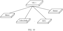
- a power supply system of the vehicle provided in this embodiment of this application may include a plurality of VIUs.
- the power supply system shown in FIG. 9 includes four VIUs: a VIU 1 to a VIU 4.
- Each VIU is integrated with the vehicle-mounted drive part provided in the foregoing embodiment, and each VIU can centrally supply power to a plurality of loads in one region of the vehicle. Therefore, the plurality of VIUs can implement distributed centralized power supply.
- Each VIU may further perform power supply management and drive control on the plurality of loads.
- the VIU 1 in the power supply system may centrally supply power to a motor, a valve body, an ECU, and a sensor in the vehicle.
- the vehicle may further include a cockpit domain controller (cockpit domain controller, CDC), a vehicle dynamic control (vehicle dynamic control, VDC) system, and a mobile data center (mobile data center, MDC).
- CDC cockpit domain controller
- VDC vehicle dynamic control
- MDC mobile data center
- this embodiment of this application provides an electronic device. Because the drive chip in the electronic device can cut off the switching transistor between the power supply and the load in response to a first fault signal, it may be ensured that a current channel between the power supply and the load is cut off in a timely manner in a fault scenario, to avoid a case in which each element in the vehicle-mounted drive part and the load are damaged when continuously operating in the fault scenario.
Landscapes
- Electronic Switches (AREA)
Applications Claiming Priority (1)
| Application Number | Priority Date | Filing Date | Title |
|---|---|---|---|
| PCT/CN2020/096858 WO2021253336A1 (zh) | 2020-06-18 | 2020-06-18 | 车载驱动电路、车载驱动芯片、车载驱动器件及电子设备 |
Publications (2)
| Publication Number | Publication Date |
|---|---|
| EP4159541A1 true EP4159541A1 (de) | 2023-04-05 |
| EP4159541A4 EP4159541A4 (de) | 2023-07-05 |
Family
ID=75699442
Family Applications (1)
| Application Number | Title | Priority Date | Filing Date |
|---|---|---|---|
| EP20940676.8A Pending EP4159541A4 (de) | 2020-06-18 | 2020-06-18 | Fahrzeugmontierte antriebsschaltung, fahrzeugmontierter antriebschip, fahrzeugmontierte antriebsvorrichtung und elektronische vorrichtung |
Country Status (3)
| Country | Link |
|---|---|
| EP (1) | EP4159541A4 (de) |
| CN (1) | CN112771780B (de) |
| WO (1) | WO2021253336A1 (de) |
Families Citing this family (6)
| Publication number | Priority date | Publication date | Assignee | Title |
|---|---|---|---|---|
| CN116409359B (zh) * | 2021-12-30 | 2025-10-17 | 比亚迪股份有限公司 | 具有自诊断功能的信号机驱动装置、方法、电子设备 |
| CN114489026B (zh) * | 2022-02-15 | 2023-08-22 | 摩登汽车有限公司 | 新能源车辆的整车控制器的测试系统 |
| CN116132495A (zh) * | 2023-02-17 | 2023-05-16 | 苏州天准科技股份有限公司 | 一种芯片控制方法、装置和电子设备 |
| CN116317483B (zh) * | 2023-05-15 | 2023-08-22 | 成都市易冲半导体有限公司 | 电荷泵驱动电路及驱动控制系统 |
| CN117707023B (zh) * | 2024-01-02 | 2024-12-10 | 苏州天准星智科技有限公司 | 一种车载域控制器芯片装置、系统及功能安全方法 |
| CN120091072B (zh) * | 2025-04-25 | 2025-07-15 | 昆山兴鸿蒙电子有限公司 | 车载总线用的适配器及其检测装置 |
Family Cites Families (12)
| Publication number | Priority date | Publication date | Assignee | Title |
|---|---|---|---|---|
| FR2701129B1 (fr) * | 1993-01-29 | 1995-03-31 | Merlin Gerin | Interface de puissance de sécurité. |
| WO1998009802A1 (en) * | 1996-09-03 | 1998-03-12 | The Nippon Signal Co., Ltd. | Apparatus for automatically controlling operation of slide of fail-safe press |
| DE102007002334B4 (de) * | 2006-01-20 | 2009-06-25 | Denso Corporation, Kariya | Überstromerkennungsschaltkreis |
| US8208235B2 (en) * | 2009-09-04 | 2012-06-26 | Lutron Electronics Co., Inc. | Method of detecting a fault condition of a load control device |
| CN201571234U (zh) * | 2009-11-27 | 2010-09-01 | 上海晶丰明源半导体有限公司 | 输出电压及电感量变化保持恒流的源级驱动led驱动电路 |
| EP2688208B1 (de) * | 2011-07-07 | 2020-04-22 | Fuji Electric Co., Ltd. | Gateansteuerungsvorrichtung |
| CN103973277B (zh) * | 2013-02-05 | 2017-06-09 | 通用电气公司 | 绝缘栅双极型晶体管的短路保护电路和方法 |
| US9762231B2 (en) * | 2015-03-10 | 2017-09-12 | Qualcomm Incorporated | Transistors configured for gate overbiasing and circuits therefrom |
| CN104837245B (zh) * | 2015-05-05 | 2016-03-30 | 深圳市稳先微电子有限公司 | 一种led驱动芯片及buck型led驱动电路 |
| ITUA20162889A1 (it) * | 2016-04-26 | 2017-10-26 | St Microelectronics Srl | Circuito di commutazione, relativo procedimento e circuito integrato |
| US10756720B2 (en) * | 2016-10-17 | 2020-08-25 | Infineon Technologies Ag | Driver circuit for electronic switch |
| CN210016447U (zh) * | 2019-03-21 | 2020-02-04 | 深圳市理邦精密仪器股份有限公司 | 保护电路和医疗设备 |
-
2020
- 2020-06-18 CN CN202080004488.9A patent/CN112771780B/zh active Active
- 2020-06-18 WO PCT/CN2020/096858 patent/WO2021253336A1/zh not_active Ceased
- 2020-06-18 EP EP20940676.8A patent/EP4159541A4/de active Pending
Also Published As
| Publication number | Publication date |
|---|---|
| WO2021253336A1 (zh) | 2021-12-23 |
| CN112771780A (zh) | 2021-05-07 |
| CN112771780B (zh) | 2022-04-08 |
| EP4159541A4 (de) | 2023-07-05 |
Similar Documents
| Publication | Publication Date | Title |
|---|---|---|
| EP4159541A1 (de) | Fahrzeugmontierte antriebsschaltung, fahrzeugmontierter antriebschip, fahrzeugmontierte antriebsvorrichtung und elektronische vorrichtung | |
| KR20000005044A (ko) | 전자유닛용 반도체 | |
| US20130320991A1 (en) | Voltage monitoring module and voltage monitoring system | |
| US11340297B2 (en) | Relay examination device and battery management system | |
| KR101893246B1 (ko) | 제어라인 진단 장치 | |
| KR102502388B1 (ko) | 차량의 eps 전원 공급 제어 장치 및 방법 | |
| CN111880088A (zh) | 继电器双边控制及诊断电路、方法、电池管理系统 | |
| WO2020120152A1 (en) | A power supply control system and method | |
| KR102851360B1 (ko) | 충전 스위치부 이상 감지 방법 및 이를 적용한 배터리 시스템 | |
| CN110907837A (zh) | 检测电路和检测方法 | |
| CN112701362A (zh) | 涉及电池单元测量的系统和方法 | |
| KR102743073B1 (ko) | 고전압 인터락 장치 및 이의 검출 방법 | |
| CN113358915B (zh) | 电压信号检测电路、供电装置及用电装置 | |
| CN215894733U (zh) | 电压信号检测电路、供电装置及用电装置 | |
| CN114347790B (zh) | 一种高压互锁检测电路及电子设备 | |
| US20210111713A1 (en) | Electronic circuit with two voltage supply circuits | |
| KR20170024818A (ko) | 제어라인 진단 장치 | |
| CN117310476A (zh) | 继电器检测电路、方法以及车辆 | |
| CN111090272A (zh) | 一种故障诊断装置、方法及车辆 | |
| CN112858894A (zh) | 接触器工作状态的检测方法、检测装置、存储介质及车辆 | |
| CN117674343A (zh) | 一种mos单元控制电路、放电控制方法及充电控制方法 | |
| CN115313801A (zh) | 用于域控制器的电源管理系统及方法 | |
| KR102948767B1 (ko) | 배터리 관리 시스템 및 방법 | |
| CN211319019U (zh) | 具有汽车功能安全设计的epb电控单元电路拓扑结构 | |
| CN115152120A (zh) | 电源装置 |
Legal Events
| Date | Code | Title | Description |
|---|---|---|---|
| STAA | Information on the status of an ep patent application or granted ep patent |
Free format text: STATUS: THE INTERNATIONAL PUBLICATION HAS BEEN MADE |
|
| PUAI | Public reference made under article 153(3) epc to a published international application that has entered the european phase |
Free format text: ORIGINAL CODE: 0009012 |
|
| STAA | Information on the status of an ep patent application or granted ep patent |
Free format text: STATUS: REQUEST FOR EXAMINATION WAS MADE |
|
| 17P | Request for examination filed |
Effective date: 20221230 |
|
| AK | Designated contracting states |
Kind code of ref document: A1 Designated state(s): AL AT BE BG CH CY CZ DE DK EE ES FI FR GB GR HR HU IE IS IT LI LT LU LV MC MK MT NL NO PL PT RO RS SE SI SK SM TR |
|
| REG | Reference to a national code |
Ref country code: DE Ref legal event code: R079 Free format text: PREVIOUS MAIN CLASS: B60R0016020000 Ipc: H03K0017100000 |
|
| A4 | Supplementary search report drawn up and despatched |
Effective date: 20230602 |
|
| RIC1 | Information provided on ipc code assigned before grant |
Ipc: B60R 16/02 20060101ALI20230526BHEP Ipc: H03K 17/06 20060101ALI20230526BHEP Ipc: H03K 17/18 20060101ALI20230526BHEP Ipc: H03K 17/082 20060101ALI20230526BHEP Ipc: H03K 17/10 20060101AFI20230526BHEP |
|
| DAV | Request for validation of the european patent (deleted) | ||
| DAX | Request for extension of the european patent (deleted) | ||
| STAA | Information on the status of an ep patent application or granted ep patent |
Free format text: STATUS: EXAMINATION IS IN PROGRESS |
|
| 17Q | First examination report despatched |
Effective date: 20240626 |
|
| RAP1 | Party data changed (applicant data changed or rights of an application transferred) |
Owner name: SHENZHEN YINWANG INTELLIGENTTECHNOLOGIES CO., LTD. |
|
| GRAP | Despatch of communication of intention to grant a patent |
Free format text: ORIGINAL CODE: EPIDOSNIGR1 |
|
| STAA | Information on the status of an ep patent application or granted ep patent |
Free format text: STATUS: GRANT OF PATENT IS INTENDED |
|
| INTG | Intention to grant announced |
Effective date: 20260305 |