EP4157553B1 - Ultraschall-bildgerät mit zeilen- und spaltenadressierung - Google Patents
Ultraschall-bildgerät mit zeilen- und spaltenadressierung Download PDFInfo
- Publication number
- EP4157553B1 EP4157553B1 EP21725780.7A EP21725780A EP4157553B1 EP 4157553 B1 EP4157553 B1 EP 4157553B1 EP 21725780 A EP21725780 A EP 21725780A EP 4157553 B1 EP4157553 B1 EP 4157553B1
- Authority
- EP
- European Patent Office
- Prior art keywords
- transducer
- transducers
- column
- electrodes
- line
- Prior art date
- Legal status (The legal status is an assumption and is not a legal conclusion. Google has not performed a legal analysis and makes no representation as to the accuracy of the status listed.)
- Active
Links
Images


Classifications
-
- B—PERFORMING OPERATIONS; TRANSPORTING
- B06—GENERATING OR TRANSMITTING MECHANICAL VIBRATIONS IN GENERAL
- B06B—METHODS OR APPARATUS FOR GENERATING OR TRANSMITTING MECHANICAL VIBRATIONS OF INFRASONIC, SONIC, OR ULTRASONIC FREQUENCY, e.g. FOR PERFORMING MECHANICAL WORK IN GENERAL
- B06B1/00—Methods or apparatus for generating mechanical vibrations of infrasonic, sonic, or ultrasonic frequency
- B06B1/02—Methods or apparatus for generating mechanical vibrations of infrasonic, sonic, or ultrasonic frequency making use of electrical energy
- B06B1/06—Methods or apparatus for generating mechanical vibrations of infrasonic, sonic, or ultrasonic frequency making use of electrical energy operating with piezoelectric effect or with electrostriction
- B06B1/0607—Methods or apparatus for generating mechanical vibrations of infrasonic, sonic, or ultrasonic frequency making use of electrical energy operating with piezoelectric effect or with electrostriction using multiple elements
- B06B1/0622—Methods or apparatus for generating mechanical vibrations of infrasonic, sonic, or ultrasonic frequency making use of electrical energy operating with piezoelectric effect or with electrostriction using multiple elements on one surface
- B06B1/0629—Square array
-
- B—PERFORMING OPERATIONS; TRANSPORTING
- B06—GENERATING OR TRANSMITTING MECHANICAL VIBRATIONS IN GENERAL
- B06B—METHODS OR APPARATUS FOR GENERATING OR TRANSMITTING MECHANICAL VIBRATIONS OF INFRASONIC, SONIC, OR ULTRASONIC FREQUENCY, e.g. FOR PERFORMING MECHANICAL WORK IN GENERAL
- B06B1/00—Methods or apparatus for generating mechanical vibrations of infrasonic, sonic, or ultrasonic frequency
- B06B1/02—Methods or apparatus for generating mechanical vibrations of infrasonic, sonic, or ultrasonic frequency making use of electrical energy
- B06B1/0292—Electrostatic transducers, e.g. electret-type
-
- B—PERFORMING OPERATIONS; TRANSPORTING
- B06—GENERATING OR TRANSMITTING MECHANICAL VIBRATIONS IN GENERAL
- B06B—METHODS OR APPARATUS FOR GENERATING OR TRANSMITTING MECHANICAL VIBRATIONS OF INFRASONIC, SONIC, OR ULTRASONIC FREQUENCY, e.g. FOR PERFORMING MECHANICAL WORK IN GENERAL
- B06B2201/00—Indexing scheme associated with B06B1/0207 for details covered by B06B1/0207 but not provided for in any of its subgroups
- B06B2201/50—Application to a particular transducer type
- B06B2201/55—Piezoelectric transducer
Definitions
- the present description relates to the field of ultrasonic imaging, and more particularly targets a device comprising a matrix of ultrasonic transducers with line-column addressing.
- An ultrasound imaging device conventionally comprises a plurality of ultrasound transducers, and an electronic control circuit connected to the transducers.
- the electronic control circuit is configured to apply electrical excitation signals to the transducers, so as to cause the emission of ultrasonic waves by the transducers, in the direction of the body or object to be analyzed.
- the ultrasonic waves emitted by the transducers are reflected by the body to be analyzed (by its internal and/or superficial structure), then return to the transducers which convert them again into electrical signals.
- These electrical response signals are read by the electronic control circuit, and can be stored and analyzed to deduce information about the body studied.
- the ultrasonic transducers can be arranged in a strip in the case of two-dimensional image acquisition devices, or in a matrix in the case of three-dimensional image acquisition devices.
- the acquired image is representative of a section of the body studied in a plane defined by the alignment axis of the transducers of the strip on the one hand, and by the direction of emission transducers on the other hand.
- the acquired image is representative of a volume defined by the two directions of alignment of the transducers of the matrix and by the direction of emission of the transducers.
- Fully populated devices provide greater flexibility in shaping transmit and receive ultrasound beams.
- the control electronics of the matrix are however complex, the number of required transmission/reception channels being equal to M*N in the case of a matrix of M lines by N columns.
- the signal-to-noise ratio is generally relatively low since each transducer has a small surface area exposed to ultrasonic waves.
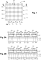
- FIG. 1 is a top view schematically and partially illustrating an example of a matrix ultrasound imaging device with line-column addressing 100.
- Each transducer 101 comprises a cavity 125 formed in a rigid support layer 127, and a flexible membrane 123 suspended above the cavity 125.
- the layer 127 is for example a layer of silicon oxide.
- the layer 127 is placed on the upper surface, for example substantially flat, of the assembly formed by the alternating strips 103 and 121.
- the cavity 125 is located opposite the lower electrode E1 of the transducer.
- each transducer 101 comprises a single cavity 125 facing its lower electrode E1.
- the cavity 125 can be divided into a plurality of elementary cavities, for example arranged, in top view, in a matrix in rows and columns, separated laterally from each other by walls lateral formed by portions of layer 127.
- a dielectric layer 129 covers the lower electrode E1 of the transducer, so as to prevent any electrical contact between the flexible membrane 123 and the electrode. lower E1 of the transducer.
- a dielectric layer (not shown) can cover the lower face of the membrane 123. In this case, layer 129 can be omitted.
- the upper electrode E2 of the transducer is arranged on and in contact with the upper face of the flexible membrane 123 of the transducer, directly above the cavity 125 and the lower electrode E1 of the transducer.
- the upper electrode E2 of each transducer 101 can be formed by the membrane itself, in which case layer 105 can be omitted.
- the device 100 can comprise a transmission circuit, a reception circuit, and a controllable switch for, in a first configuration, connecting the electrodes E1 of the transducers of the column to an output terminal of the column transmission circuit, and, in a second configuration, connect the electrodes E1 of the column transducers to an input terminal of the column reception circuit.
- a limitation of the device of the figure 1 is linked to the fact that the capacitive coupling between the lower electrode strips 103 and the substrate 110 is much greater than the capacitive coupling between the upper electrode strips 105 and the substrate 110. This results in a difference in behavior between the lines L i and the columns C j of the device. More particularly, this results in a difference in reception sensitivity between the lines L i and the columns C j of the device.
- the voltage generated on the upper electrode strip 105 of a line L i during a reading phase of the line L i is significantly greater than the voltage generated on the lower electrode strip 103 of a column C j during a reading phase of column C j . This can lead to unwanted artifacts in the acquired image.
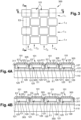
- FIG. 3 is a top view schematically and partially illustrating an example of an embodiment of a matrix ultrasound imaging device with line-column addressing 300.
- FIGS. 4A and 4B are sectional views of the device 300 of the Figure 3 according to respectively plans AA and BB of the Figure 3 .
- the device 300 has elements in common with the device 100 described previously. These common elements will not be detailed again below. In the remainder of the description, only the differences compared to the device 100 will be highlighted.
- the device 300 comprises a plurality of ultrasonic transducers 101 arranged in a matrix along M lines L i and N columns C j .
- each transducer 101 of the device 300 comprises a lower electrode E1 and an upper electrode E2.
- the upper electrodes E2 are represented on the Figure 3 .
- the device 300 differs from the device 100 mainly by the interconnection diagram of the lower electrodes E1 and upper electrodes E2 of the transducers 101 of the device.
- any two neighboring transducers 101 ij and 101 i+1j in the column respectively have their lower electrode E1 and their upper electrode E2 connected to each other, or their upper electrode E2 and their lower electrode E1 connected to each other.
- the upper electrodes E2 of the transducers 101 ij and 101 i+1j are, however, electrically isolated from each other.
- the lower electrodes E1 of the transducers 101 ij and 101 i+1j are electrically isolated from each other.
- connection elements 311 for example made of metal, vertically crossing the portions of the dielectric layer 127 laterally separating the cavities 125 of the transducers. More particularly, in the example of Figures 4A and 4B , each connection element 311 extends vertically from the lower face of the upper electrode E2 of a transducer 101 to the upper face of the lower electrode E1 of a neighboring transducer 101.
- the dielectric regions 121 form, in top view, a continuous grid entirely surrounding each electrode E1 and laterally separating each electrode E1 from the electrodes E1 of neighboring transducers.
- each electrode E2 is entirely surrounded and laterally separated from the electrodes E2 of neighboring transducers by a dielectric region (possibly air or vacuum).
- each flexible membrane 123 is entirely surrounded and separated laterally from the membranes 123 of neighboring transducers by a dielectric region.
- the flexible membranes 123 can be made of a dielectric material, for example silicon oxide.
- the membranes of neighboring transducers can form a continuous layer.
- the device 300 can comprise a transmission circuit, a reception circuit, and a controllable switch for, in a first configuration, connecting the line conductor 305 of the line L i to an output terminal of the transmission circuit of the line, and, in a second configuration, connect the line conductor 305 of the line L i to an input terminal of the reception circuit of the line.
- the device 300 can comprise a transmission circuit, a reception circuit, and a controllable switch for, in a first configuration, connecting the column conductor 303 of the column C j to an output terminal of the column's transmission circuit, and, in a second configuration, connect the column conductor 303 of column C j to an input terminal of the column's reception circuit.
- An advantage of the device 300 is that the capacitive coupling of the line conductors 305 with the substrate 110 and the capacitive coupling of the column conductors 303 with the substrate 110 are substantially identical. This makes it possible to symmetrize the behavior of the lines L i and the columns C j of the device.
- the reception sensitivity is substantially identical in the rows and in the columns of the device, which makes it possible to improve the quality of the images acquired. This also makes it possible to have significantly the same electrical properties, and in particular substantially the same impedance, on the rows and columns.
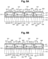
- FIGS. 5A and 5B are sectional views respectively according to planes AA and BB of the Figure 3 , illustrating a variant embodiment of the device 300.
- each electrode E1 of the device differs from what has been described previously in relation to the Figures 3, 4A and 4B mainly in that, in this variant, under each electrode E1 of the device, a portion of metal layer 501 extends, for example made of the same metal as the upper electrodes E2 of the device.
- Layer 501 is in contact, via its upper face, with the lower face of the electrodes E1.
- layer 501 is in contact, via its lower face, with the upper face of dielectric layer 112.
- each connection element 311 extends vertically from the lower face of the upper electrode.
- E2 of a transducer 101 to the upper face of the metal layer portion 501 of a neighboring transducer 101.
- An advantage of this alternative embodiment is that it allows, in the case where the lower electrodes E1 of the transducers are made of a semiconductor material, to increase the electrical conductivity of the conductive elements of row 305 and column 303 at the level of the lower electrodes E1 of transducers.
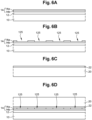
- FIG. 6A illustrates a step of oxidation of part of the thickness of a semiconductor layer of an SOI type structure (from the English "Semiconductor On Insulator” - semiconductor on insulator).
- the initial structure comprises a support substrate 10, for example made of a semiconductor material, for example silicon, a dielectric layer 12, for example silicon oxide, covering the upper face of the substrate 10, and a semiconductor layer 14, for example example a layer of monocrystalline silicon, covering the upper face of the dielectric layer 12.
- the dielectric layer 12 and the upper semiconductor layer 14 each extend, for example, continuously and with a substantially constant thickness, over the entire upper surface of the substrate 10. In this example, the dielectric layer 12 is in contact, via its lower face, with the upper face of the substrate 10, and the semiconductor layer 14 is in contact, via its lower face, with the upper face of the dielectric layer 12 .
- the oxidation of the upper part of layer 14 is carried out by a dry thermal oxidation process.
- the initial thickness of the semiconductor layer 14 is for example between 50 nm and 3 ⁇ m.
- the thickness of the insulating layer 14a after oxidation is for example between 10 and 500 nm, for example of the order of 50 nm.
- the cavities 125 extend vertically from the upper face of the insulating layer 14a, towards the layer 14b. In the example shown, the cavities 125 are through, that is to say they open onto the upper face of the semiconductor layer 14b.
- FIG. 6F illustrates a step of forming insulating trenches 121 filled with a dielectric material, for example silicon oxide, from the upper face of the thinned substrate 20.
- Trenches 121 (in black on the figure 6F ) correspond to the dielectric regions 121 of the Figures 4A and 4B .
- the trenches 121 pass entirely through the substrate 20, over its entire thickness, and open onto the upper face of the insulating layer 22.
- the trenches 121 are for example formed by deep ionic reactive etching of the substrate 20, then filled with a dielectric material.
- the portions of substrate 20 delimited by the trenches correspond to the electrodes E1 of the transducers.
- FIG. 6G illustrates a step of oxidation of the upper face of a third semiconductor substrate 30, for example made of silicon.
- a dielectric layer 32 for example made of silicon oxide
- the oxidation can be carried out by a dry thermal oxidation process.
- the thickness of the dielectric layer 32 formed during this step is for example between 100 nm and 10 ⁇ m, for example of the order of 2 ⁇ m, for example between 2 and 10 ⁇ m.
- the layer 32 can be formed by depositing an insulating material, for example silicon oxide, on the upper face of the substrate 30.
- the substrate 30 can be a substrate made of a dielectric material, for example glass, or a high resistivity semiconductor substrate, for example an undoped or lightly doped silicon substrate.
- FIG. 6H illustrates a step of reporting the structure of the figure 6F on the structure of the figure 6G .
- the structure of the figure 6F is returned relative to the orientation of the figure 6F , and transferred to the structure of the figure 6G so that the lower face of the electrodes E1 and the lower face of the dielectric regions 121 come into contact with the upper face of the dielectric layer 32.
- the two structures are fixed to each other by direct bonding of the lower face of the electrodes E1 and dielectric regions 121 on the upper face of the dielectric layer 32.
- FIG. 6I illustrates a subsequent step of removing the substrate 10 and the dielectric layer 12 from the starting structure.
- the semiconductor layer 14b is kept above the cavities, to form the membranes 123 of the transducers.
Landscapes
- Engineering & Computer Science (AREA)
- Mechanical Engineering (AREA)
- Transducers For Ultrasonic Waves (AREA)
- Ultra Sonic Daignosis Equipment (AREA)
- Investigating Or Analyzing Materials By The Use Of Ultrasonic Waves (AREA)
Claims (9)
- Ultraschallbildgebungsvorrichtung (300), die eine Vielzahl von Ultraschallwandlern (101) aufweist, die in Reihen (Li) und Spalten (Cj) angeordnet sind, wobei jeder Wandler (101) eine untere Elektrode (E1) und eine obere Elektrode (E2) aufweist, wobei:- und zwar in jeder Reihe (Li), zwei beliebige benachbarte Wandler (101) in der Reihe jeweils ihre untere Elektrode (E1) und ihre obere Elektrode (E2) miteinander verbunden haben, oder ihre obere Elektrode (E2) und ihre untere Elektrode (E1) miteinander verbunden haben; und- und zwar in jeder Spalte (Cj), zwei beliebige benachbarte Wandler (101) in der Spalte jeweils ihre untere Elektrode (E1) und ihre obere Elektrode (E2) miteinander verbunden haben, oder ihre obere Elektrode (E2) und ihre untere Elektrode (E1) miteinander verbunden haben.
- Vorrichtung nach Anspruch 1, wobei:- und zwar in jeder Reihe (Li), zwei beliebige benachbarte Wandler (101) in der Reihe ihre jeweiligen unteren Elektroden (E1) elektrisch voneinander isoliert haben und ihre jeweiligen oberen Elektroden (E2) elektrisch voneinander isoliert haben; und- und zwar in jeder Spalte (Cj), zwei beliebige benachbarte Wandler (101) in der Spalte ihre jeweiligen unteren Elektroden (E1) elektrisch voneinander isoliert haben und ihre jeweiligen oberen Elektroden (E2) elektrisch voneinander isoliert haben.
- Vorrichtung nach Anspruch 1 oder 2, wobei jeder Ultraschallwandler (101) ein CMUT-Wandler ist, der eine flexible Membran (123) aufweist, die über einem Hohlraum (125) aufgehängt ist, wobei die untere Elektrode (E1) des Wandlers auf der Seite des Hohlraums (125) angeordnet ist, die der flexiblen Membran (123) gegenüberliegt, und wobei die obere Elektrode (E2) des Wandlers auf der Seite der flexiblen Membran (123) angeordnet ist, die dem Hohlraum (125) gegenüberliegt.
- Vorrichtung nach Anspruch 3, wobei die Hohlräume (125) der Wandler (101) in einer starren Trägerschicht (127) ausgebildet sind und wobei jeder Wandler (101) mit seiner oberen Elektrode (E2) über ein leitendes Element (311), das die starre Trägerschicht (127) überquert, mit einer unteren Elektrode (E1) eines benachbarten Wandlers (101) elektrisch verbunden ist.
- Vorrichtung nach Anspruch 3 oder 4, wobei die untere Elektrode (E1) eines jeden Wandlers (101) aus einem dotierten Halbleitermaterial gefertigt ist.
- Vorrichtung nach Anspruch 5, wobei sich ein Metallschichtteil (501) unter der unteren Elektrode (E1) eines jeden Wandlers (101) erstreckt, und zwar in Kontakt mit der unteren Oberfläche der unteren Elektrode (E1) des Wandlers.
- Vorrichtung nach einem der Ansprüche 3 bis 6, wobei, in jedem Wandler (101), die flexible Membran (123) aus einem Halbleitermaterial gefertigt ist.
- Vorrichtung nach einem der Ansprüche 3 bis 7, wobei, in jedem Wandler (101), eine dielektrische Schicht (129) die obere Oberfläche der unteren Elektrode (E1) des Wandlers bedeckt, und zwar am Boden des Hohlraums (125).
- Vorrichtung nach Anspruch 1 oder 2, wobei jeder Wandler (101) ein PMUT-Wandler ist.
Applications Claiming Priority (2)
| Application Number | Priority Date | Filing Date | Title |
|---|---|---|---|
| FR2005636A FR3110834B1 (fr) | 2020-05-28 | 2020-05-28 | Dispositif d'imagerie ultrasonore à adressage ligne-colonne |
| PCT/EP2021/063218 WO2021239525A1 (fr) | 2020-05-28 | 2021-05-19 | Dispositif d'imagerie ultrasonore a adressage ligne-colonne |
Publications (2)
| Publication Number | Publication Date |
|---|---|
| EP4157553A1 EP4157553A1 (de) | 2023-04-05 |
| EP4157553B1 true EP4157553B1 (de) | 2024-07-10 |
Family
ID=73138881
Family Applications (1)
| Application Number | Title | Priority Date | Filing Date |
|---|---|---|---|
| EP21725780.7A Active EP4157553B1 (de) | 2020-05-28 | 2021-05-19 | Ultraschall-bildgerät mit zeilen- und spaltenadressierung |
Country Status (9)
| Country | Link |
|---|---|
| US (1) | US12233435B2 (de) |
| EP (1) | EP4157553B1 (de) |
| JP (1) | JP2023527436A (de) |
| KR (1) | KR20230017256A (de) |
| CN (1) | CN115666799B (de) |
| CA (1) | CA3181376A1 (de) |
| DK (1) | DK4157553T3 (de) |
| FR (1) | FR3110834B1 (de) |
| WO (1) | WO2021239525A1 (de) |
Families Citing this family (2)
| Publication number | Priority date | Publication date | Assignee | Title |
|---|---|---|---|---|
| CN116493234B (zh) * | 2023-04-26 | 2025-04-15 | 西安交通大学 | 一种基于KNN和应力释放凹槽的TFT-PMUTs、制备方法、应用和超声触觉感知检测设备 |
| TWI897033B (zh) * | 2023-09-14 | 2025-09-11 | 佳世達科技股份有限公司 | 超聲波換能器及其製造方法 |
Family Cites Families (9)
| Publication number | Priority date | Publication date | Assignee | Title |
|---|---|---|---|---|
| US7122398B1 (en) * | 2004-03-25 | 2006-10-17 | Nanosolar, Inc. | Manufacturing of optoelectronic devices |
| JP5578810B2 (ja) * | 2009-06-19 | 2014-08-27 | キヤノン株式会社 | 静電容量型の電気機械変換装置 |
| JP2011056103A (ja) * | 2009-09-11 | 2011-03-24 | Fujifilm Corp | 超音波プローブおよび超音波診断装置 |
| JP6221582B2 (ja) * | 2013-09-30 | 2017-11-01 | セイコーエプソン株式会社 | 超音波デバイスおよびプローブ並びに電子機器および超音波画像装置 |
| WO2015071387A1 (en) * | 2013-11-18 | 2015-05-21 | Koninklijke Philips N.V. | Ultrasound transducer assembly |
| WO2016139103A1 (en) * | 2015-03-03 | 2016-09-09 | Koninklijke Philips N.V. | A cmut array comprising an acoustic window layer |
| US11084062B2 (en) * | 2015-11-02 | 2021-08-10 | Koninklijke Philips N.V. | Ultrasound transducer array, probe and system |
| AU2017281280B2 (en) * | 2016-06-20 | 2022-01-06 | Butterfly Network, Inc. | Electrical contact arrangement for microfabricated ultrasonic transducer |
| JP6782649B2 (ja) * | 2017-02-28 | 2020-11-11 | 株式会社日立製作所 | 超音波撮像装置 |
-
2020
- 2020-05-28 FR FR2005636A patent/FR3110834B1/fr not_active Expired - Fee Related
-
2021
- 2021-05-19 WO PCT/EP2021/063218 patent/WO2021239525A1/fr not_active Ceased
- 2021-05-19 US US17/927,323 patent/US12233435B2/en active Active
- 2021-05-19 EP EP21725780.7A patent/EP4157553B1/de active Active
- 2021-05-19 CN CN202180039130.4A patent/CN115666799B/zh active Active
- 2021-05-19 CA CA3181376A patent/CA3181376A1/fr active Pending
- 2021-05-19 KR KR1020227045304A patent/KR20230017256A/ko not_active Ceased
- 2021-05-19 DK DK21725780.7T patent/DK4157553T3/da active
- 2021-05-19 JP JP2022573396A patent/JP2023527436A/ja active Pending
Also Published As
| Publication number | Publication date |
|---|---|
| DK4157553T3 (da) | 2024-10-14 |
| JP2023527436A (ja) | 2023-06-28 |
| FR3110834A1 (fr) | 2021-12-03 |
| WO2021239525A1 (fr) | 2021-12-02 |
| CN115666799A (zh) | 2023-01-31 |
| CN115666799B (zh) | 2026-02-06 |
| US12233435B2 (en) | 2025-02-25 |
| FR3110834B1 (fr) | 2022-04-22 |
| EP4157553A1 (de) | 2023-04-05 |
| KR20230017256A (ko) | 2023-02-03 |
| CA3181376A1 (fr) | 2021-12-02 |
| US20230201875A1 (en) | 2023-06-29 |
Similar Documents
| Publication | Publication Date | Title |
|---|---|---|
| US7545075B2 (en) | Capacitive micromachined ultrasonic transducer array with through-substrate electrical connection and method of fabricating same | |
| EP4157553B1 (de) | Ultraschall-bildgerät mit zeilen- und spaltenadressierung | |
| FR2917841A1 (fr) | Systeme ultrasonore a structure d'interconnexion par traversees | |
| FR2881913A1 (fr) | Transducteur capacitif tres sensible (a micro-usinage) micro-usine a ultrasons | |
| EP3714544A1 (de) | Verfahren zur herstellung eines volumenwellenresonators mit reduzierter parasitärer kapazität | |
| FR2862161A1 (fr) | Procede de fabrication d'un transducteur acoustique en ceramique multicouche | |
| FR2460085A1 (fr) | Procede pour la realisation de transducteurs ultra-acoustiques a raies ou a matrice de points et transducteurs ainsi obtenus | |
| FR2879022A1 (fr) | Composants electroniques superposes pour capteurs. | |
| EP2306641B1 (de) | Herstellungsverfahren eines BAW-Resonators mit hohem Qualitätsfaktor | |
| FR3060844A1 (fr) | Dispositif microelectronique acoustique | |
| EP4143606B1 (de) | Ultraschallbildgebungsvorrichtung | |
| EP3987663B1 (de) | Ultraschallbildsensor mit matrixstruktur | |
| EP4359784B1 (de) | Verfahren und vorrichtung für ultraschallbildgebung mittels zeile-spalte addressieren | |
| EP1536439B1 (de) | Variablen Kondensator enthaltendes Bauteil | |
| EP1953778B1 (de) | Kondensator in einem Festkörperschaltkreis | |
| FR3155598A1 (fr) | Sonde ultrasonore à transducteurs MUT et méthode de fabrication d’une telle sonde | |
| FR3152939A1 (fr) | Transducteur PMUT | |
| WO2026008205A1 (fr) | Sonde ultrasonore et procédé d'imagerie intravasculaire par ultrasons | |
| EP4705039A1 (de) | Verfahren zur herstellung eines cmut-wandlers | |
| EP4282543A1 (de) | Cmut-wandler und verfahren zur herstellung eines cmut-wandlers | |
| FR3160483A1 (fr) | Dispositif haptique mid-air avec fonction de récupération d’énergie et procédé de fabrication dudit dispositif haptique | |
| WO2024245779A1 (fr) | Procede et dispositif d'imagerie ultrasonore a adressage ligne-colonne | |
| FR3159384A1 (fr) | Méthode de fabrication d’une sonde ultrasonore, et sonde ultrasonore |
Legal Events
| Date | Code | Title | Description |
|---|---|---|---|
| STAA | Information on the status of an ep patent application or granted ep patent |
Free format text: STATUS: UNKNOWN |
|
| STAA | Information on the status of an ep patent application or granted ep patent |
Free format text: STATUS: THE INTERNATIONAL PUBLICATION HAS BEEN MADE |
|
| PUAI | Public reference made under article 153(3) epc to a published international application that has entered the european phase |
Free format text: ORIGINAL CODE: 0009012 |
|
| STAA | Information on the status of an ep patent application or granted ep patent |
Free format text: STATUS: REQUEST FOR EXAMINATION WAS MADE |
|
| 17P | Request for examination filed |
Effective date: 20221205 |
|
| AK | Designated contracting states |
Kind code of ref document: A1 Designated state(s): AL AT BE BG CH CY CZ DE DK EE ES FI FR GB GR HR HU IE IS IT LI LT LU LV MC MK MT NL NO PL PT RO RS SE SI SK SM TR |
|
| DAV | Request for validation of the european patent (deleted) | ||
| DAX | Request for extension of the european patent (deleted) | ||
| GRAP | Despatch of communication of intention to grant a patent |
Free format text: ORIGINAL CODE: EPIDOSNIGR1 |
|
| STAA | Information on the status of an ep patent application or granted ep patent |
Free format text: STATUS: GRANT OF PATENT IS INTENDED |
|
| INTG | Intention to grant announced |
Effective date: 20240318 |
|
| GRAS | Grant fee paid |
Free format text: ORIGINAL CODE: EPIDOSNIGR3 |
|
| P01 | Opt-out of the competence of the unified patent court (upc) registered |
Effective date: 20240405 |
|
| GRAA | (expected) grant |
Free format text: ORIGINAL CODE: 0009210 |
|
| STAA | Information on the status of an ep patent application or granted ep patent |
Free format text: STATUS: THE PATENT HAS BEEN GRANTED |
|
| AK | Designated contracting states |
Kind code of ref document: B1 Designated state(s): AL AT BE BG CH CY CZ DE DK EE ES FI FR GB GR HR HU IE IS IT LI LT LU LV MC MK MT NL NO PL PT RO RS SE SI SK SM TR |
|
| REG | Reference to a national code |
Ref country code: CH Ref legal event code: EP |
|
| REG | Reference to a national code |
Ref country code: DE Ref legal event code: R096 Ref document number: 602021015504 Country of ref document: DE |
|
| REG | Reference to a national code |
Ref country code: NL Ref legal event code: FP |
|
| REG | Reference to a national code |
Ref country code: DK Ref legal event code: T3 Effective date: 20241007 |
|
| REG | Reference to a national code |
Ref country code: LT Ref legal event code: MG9D |
|
| PG25 | Lapsed in a contracting state [announced via postgrant information from national office to epo] |
Ref country code: PT Free format text: LAPSE BECAUSE OF FAILURE TO SUBMIT A TRANSLATION OF THE DESCRIPTION OR TO PAY THE FEE WITHIN THE PRESCRIBED TIME-LIMIT Effective date: 20241111 |
|
| REG | Reference to a national code |
Ref country code: AT Ref legal event code: MK05 Ref document number: 1701605 Country of ref document: AT Kind code of ref document: T Effective date: 20240710 |
|
| PG25 | Lapsed in a contracting state [announced via postgrant information from national office to epo] |
Ref country code: PT Free format text: LAPSE BECAUSE OF FAILURE TO SUBMIT A TRANSLATION OF THE DESCRIPTION OR TO PAY THE FEE WITHIN THE PRESCRIBED TIME-LIMIT Effective date: 20241111 |
|
| PG25 | Lapsed in a contracting state [announced via postgrant information from national office to epo] |
Ref country code: NO Free format text: LAPSE BECAUSE OF FAILURE TO SUBMIT A TRANSLATION OF THE DESCRIPTION OR TO PAY THE FEE WITHIN THE PRESCRIBED TIME-LIMIT Effective date: 20241010 |
|
| PG25 | Lapsed in a contracting state [announced via postgrant information from national office to epo] |
Ref country code: FI Free format text: LAPSE BECAUSE OF FAILURE TO SUBMIT A TRANSLATION OF THE DESCRIPTION OR TO PAY THE FEE WITHIN THE PRESCRIBED TIME-LIMIT Effective date: 20240710 Ref country code: GR Free format text: LAPSE BECAUSE OF FAILURE TO SUBMIT A TRANSLATION OF THE DESCRIPTION OR TO PAY THE FEE WITHIN THE PRESCRIBED TIME-LIMIT Effective date: 20241011 Ref country code: PL Free format text: LAPSE BECAUSE OF FAILURE TO SUBMIT A TRANSLATION OF THE DESCRIPTION OR TO PAY THE FEE WITHIN THE PRESCRIBED TIME-LIMIT Effective date: 20240710 |
|
| PG25 | Lapsed in a contracting state [announced via postgrant information from national office to epo] |
Ref country code: BG Free format text: LAPSE BECAUSE OF FAILURE TO SUBMIT A TRANSLATION OF THE DESCRIPTION OR TO PAY THE FEE WITHIN THE PRESCRIBED TIME-LIMIT Effective date: 20240710 |
|
| PG25 | Lapsed in a contracting state [announced via postgrant information from national office to epo] |
Ref country code: LV Free format text: LAPSE BECAUSE OF FAILURE TO SUBMIT A TRANSLATION OF THE DESCRIPTION OR TO PAY THE FEE WITHIN THE PRESCRIBED TIME-LIMIT Effective date: 20240710 |
|
| PG25 | Lapsed in a contracting state [announced via postgrant information from national office to epo] |
Ref country code: AT Free format text: LAPSE BECAUSE OF FAILURE TO SUBMIT A TRANSLATION OF THE DESCRIPTION OR TO PAY THE FEE WITHIN THE PRESCRIBED TIME-LIMIT Effective date: 20240710 Ref country code: IS Free format text: LAPSE BECAUSE OF FAILURE TO SUBMIT A TRANSLATION OF THE DESCRIPTION OR TO PAY THE FEE WITHIN THE PRESCRIBED TIME-LIMIT Effective date: 20241110 |
|
| PG25 | Lapsed in a contracting state [announced via postgrant information from national office to epo] |
Ref country code: HR Free format text: LAPSE BECAUSE OF FAILURE TO SUBMIT A TRANSLATION OF THE DESCRIPTION OR TO PAY THE FEE WITHIN THE PRESCRIBED TIME-LIMIT Effective date: 20240710 |
|
| PG25 | Lapsed in a contracting state [announced via postgrant information from national office to epo] |
Ref country code: RS Free format text: LAPSE BECAUSE OF FAILURE TO SUBMIT A TRANSLATION OF THE DESCRIPTION OR TO PAY THE FEE WITHIN THE PRESCRIBED TIME-LIMIT Effective date: 20241010 Ref country code: ES Free format text: LAPSE BECAUSE OF FAILURE TO SUBMIT A TRANSLATION OF THE DESCRIPTION OR TO PAY THE FEE WITHIN THE PRESCRIBED TIME-LIMIT Effective date: 20240710 |
|
| PG25 | Lapsed in a contracting state [announced via postgrant information from national office to epo] |
Ref country code: RS Free format text: LAPSE BECAUSE OF FAILURE TO SUBMIT A TRANSLATION OF THE DESCRIPTION OR TO PAY THE FEE WITHIN THE PRESCRIBED TIME-LIMIT Effective date: 20241010 Ref country code: PL Free format text: LAPSE BECAUSE OF FAILURE TO SUBMIT A TRANSLATION OF THE DESCRIPTION OR TO PAY THE FEE WITHIN THE PRESCRIBED TIME-LIMIT Effective date: 20240710 Ref country code: NO Free format text: LAPSE BECAUSE OF FAILURE TO SUBMIT A TRANSLATION OF THE DESCRIPTION OR TO PAY THE FEE WITHIN THE PRESCRIBED TIME-LIMIT Effective date: 20241010 Ref country code: LV Free format text: LAPSE BECAUSE OF FAILURE TO SUBMIT A TRANSLATION OF THE DESCRIPTION OR TO PAY THE FEE WITHIN THE PRESCRIBED TIME-LIMIT Effective date: 20240710 Ref country code: IS Free format text: LAPSE BECAUSE OF FAILURE TO SUBMIT A TRANSLATION OF THE DESCRIPTION OR TO PAY THE FEE WITHIN THE PRESCRIBED TIME-LIMIT Effective date: 20241110 Ref country code: HR Free format text: LAPSE BECAUSE OF FAILURE TO SUBMIT A TRANSLATION OF THE DESCRIPTION OR TO PAY THE FEE WITHIN THE PRESCRIBED TIME-LIMIT Effective date: 20240710 Ref country code: GR Free format text: LAPSE BECAUSE OF FAILURE TO SUBMIT A TRANSLATION OF THE DESCRIPTION OR TO PAY THE FEE WITHIN THE PRESCRIBED TIME-LIMIT Effective date: 20241011 Ref country code: FI Free format text: LAPSE BECAUSE OF FAILURE TO SUBMIT A TRANSLATION OF THE DESCRIPTION OR TO PAY THE FEE WITHIN THE PRESCRIBED TIME-LIMIT Effective date: 20240710 Ref country code: ES Free format text: LAPSE BECAUSE OF FAILURE TO SUBMIT A TRANSLATION OF THE DESCRIPTION OR TO PAY THE FEE WITHIN THE PRESCRIBED TIME-LIMIT Effective date: 20240710 Ref country code: BG Free format text: LAPSE BECAUSE OF FAILURE TO SUBMIT A TRANSLATION OF THE DESCRIPTION OR TO PAY THE FEE WITHIN THE PRESCRIBED TIME-LIMIT Effective date: 20240710 Ref country code: AT Free format text: LAPSE BECAUSE OF FAILURE TO SUBMIT A TRANSLATION OF THE DESCRIPTION OR TO PAY THE FEE WITHIN THE PRESCRIBED TIME-LIMIT Effective date: 20240710 |
|
| REG | Reference to a national code |
Ref country code: DE Ref legal event code: R097 Ref document number: 602021015504 Country of ref document: DE |
|
| PG25 | Lapsed in a contracting state [announced via postgrant information from national office to epo] |
Ref country code: SM Free format text: LAPSE BECAUSE OF FAILURE TO SUBMIT A TRANSLATION OF THE DESCRIPTION OR TO PAY THE FEE WITHIN THE PRESCRIBED TIME-LIMIT Effective date: 20240710 Ref country code: RO Free format text: LAPSE BECAUSE OF FAILURE TO SUBMIT A TRANSLATION OF THE DESCRIPTION OR TO PAY THE FEE WITHIN THE PRESCRIBED TIME-LIMIT Effective date: 20240710 |
|
| PG25 | Lapsed in a contracting state [announced via postgrant information from national office to epo] |
Ref country code: EE Free format text: LAPSE BECAUSE OF FAILURE TO SUBMIT A TRANSLATION OF THE DESCRIPTION OR TO PAY THE FEE WITHIN THE PRESCRIBED TIME-LIMIT Effective date: 20240710 |
|
| PG25 | Lapsed in a contracting state [announced via postgrant information from national office to epo] |
Ref country code: CZ Free format text: LAPSE BECAUSE OF FAILURE TO SUBMIT A TRANSLATION OF THE DESCRIPTION OR TO PAY THE FEE WITHIN THE PRESCRIBED TIME-LIMIT Effective date: 20240710 |
|
| PG25 | Lapsed in a contracting state [announced via postgrant information from national office to epo] |
Ref country code: SK Free format text: LAPSE BECAUSE OF FAILURE TO SUBMIT A TRANSLATION OF THE DESCRIPTION OR TO PAY THE FEE WITHIN THE PRESCRIBED TIME-LIMIT Effective date: 20240710 |
|
| PGFP | Annual fee paid to national office [announced via postgrant information from national office to epo] |
Ref country code: NL Payment date: 20250429 Year of fee payment: 5 |
|
| PLBE | No opposition filed within time limit |
Free format text: ORIGINAL CODE: 0009261 |
|
| STAA | Information on the status of an ep patent application or granted ep patent |
Free format text: STATUS: NO OPPOSITION FILED WITHIN TIME LIMIT |
|
| 26N | No opposition filed |
Effective date: 20250411 |
|
| PGFP | Annual fee paid to national office [announced via postgrant information from national office to epo] |
Ref country code: DE Payment date: 20250513 Year of fee payment: 5 |
|
| PGFP | Annual fee paid to national office [announced via postgrant information from national office to epo] |
Ref country code: GB Payment date: 20250521 Year of fee payment: 5 Ref country code: DK Payment date: 20250428 Year of fee payment: 5 |
|
| PGFP | Annual fee paid to national office [announced via postgrant information from national office to epo] |
Ref country code: IT Payment date: 20250508 Year of fee payment: 5 |
|
| PGFP | Annual fee paid to national office [announced via postgrant information from national office to epo] |
Ref country code: FR Payment date: 20250528 Year of fee payment: 5 |
|
| PG25 | Lapsed in a contracting state [announced via postgrant information from national office to epo] |
Ref country code: SE Free format text: LAPSE BECAUSE OF FAILURE TO SUBMIT A TRANSLATION OF THE DESCRIPTION OR TO PAY THE FEE WITHIN THE PRESCRIBED TIME-LIMIT Effective date: 20240710 |
|
| REG | Reference to a national code |
Ref country code: CH Ref legal event code: H13 Free format text: ST27 STATUS EVENT CODE: U-0-0-H10-H13 (AS PROVIDED BY THE NATIONAL OFFICE) Effective date: 20251223 |
|
| PG25 | Lapsed in a contracting state [announced via postgrant information from national office to epo] |
Ref country code: LU Free format text: LAPSE BECAUSE OF NON-PAYMENT OF DUE FEES Effective date: 20250519 |
|
| PG25 | Lapsed in a contracting state [announced via postgrant information from national office to epo] |
Ref country code: CH Free format text: LAPSE BECAUSE OF NON-PAYMENT OF DUE FEES Effective date: 20250531 |
|
| REG | Reference to a national code |
Ref country code: BE Ref legal event code: MM Effective date: 20250531 |
|
| PG25 | Lapsed in a contracting state [announced via postgrant information from national office to epo] |
Ref country code: MC Free format text: LAPSE BECAUSE OF FAILURE TO SUBMIT A TRANSLATION OF THE DESCRIPTION OR TO PAY THE FEE WITHIN THE PRESCRIBED TIME-LIMIT Effective date: 20240710 |