EP4156252A1 - Semiconductor module - Google Patents
Semiconductor module Download PDFInfo
- Publication number
- EP4156252A1 EP4156252A1 EP20936107.0A EP20936107A EP4156252A1 EP 4156252 A1 EP4156252 A1 EP 4156252A1 EP 20936107 A EP20936107 A EP 20936107A EP 4156252 A1 EP4156252 A1 EP 4156252A1
- Authority
- EP
- European Patent Office
- Prior art keywords
- relay plate
- semiconductor module
- bonding wire
- plate
- relay
- Prior art date
- Legal status (The legal status is an assumption and is not a legal conclusion. Google has not performed a legal analysis and makes no representation as to the accuracy of the status listed.)
- Granted
Links
Images


Classifications
-
- H—ELECTRICITY
- H10—SEMICONDUCTOR DEVICES; ELECTRIC SOLID-STATE DEVICES NOT OTHERWISE PROVIDED FOR
- H10W—GENERIC PACKAGES, INTERCONNECTIONS, CONNECTORS OR OTHER CONSTRUCTIONAL DETAILS OF DEVICES COVERED BY CLASS H10
- H10W70/00—Package substrates; Interposers; Redistribution layers [RDL]
- H10W70/40—Leadframes
- H10W70/464—Additional interconnections in combination with leadframes
- H10W70/465—Bumps or wires
-
- H—ELECTRICITY
- H02—GENERATION; CONVERSION OR DISTRIBUTION OF ELECTRIC POWER
- H02M—APPARATUS FOR CONVERSION BETWEEN AC AND AC, BETWEEN AC AND DC, OR BETWEEN DC AND DC, AND FOR USE WITH MAINS OR SIMILAR POWER SUPPLY SYSTEMS; CONVERSION OF DC OR AC INPUT POWER INTO SURGE OUTPUT POWER; CONTROL OR REGULATION THEREOF
- H02M7/00—Conversion of AC power input into DC power output; Conversion of DC power input into AC power output
- H02M7/003—Constructional details, e.g. physical layout, assembly, wiring or busbar connections
-
- H—ELECTRICITY
- H10—SEMICONDUCTOR DEVICES; ELECTRIC SOLID-STATE DEVICES NOT OTHERWISE PROVIDED FOR
- H10W—GENERIC PACKAGES, INTERCONNECTIONS, CONNECTORS OR OTHER CONSTRUCTIONAL DETAILS OF DEVICES COVERED BY CLASS H10
- H10W70/00—Package substrates; Interposers; Redistribution layers [RDL]
- H10W70/40—Leadframes
- H10W70/421—Shapes or dispositions
-
- H—ELECTRICITY
- H10—SEMICONDUCTOR DEVICES; ELECTRIC SOLID-STATE DEVICES NOT OTHERWISE PROVIDED FOR
- H10W—GENERIC PACKAGES, INTERCONNECTIONS, CONNECTORS OR OTHER CONSTRUCTIONAL DETAILS OF DEVICES COVERED BY CLASS H10
- H10W70/00—Package substrates; Interposers; Redistribution layers [RDL]
- H10W70/40—Leadframes
- H10W70/464—Additional interconnections in combination with leadframes
-
- H—ELECTRICITY
- H10—SEMICONDUCTOR DEVICES; ELECTRIC SOLID-STATE DEVICES NOT OTHERWISE PROVIDED FOR
- H10W—GENERIC PACKAGES, INTERCONNECTIONS, CONNECTORS OR OTHER CONSTRUCTIONAL DETAILS OF DEVICES COVERED BY CLASS H10
- H10W70/00—Package substrates; Interposers; Redistribution layers [RDL]
- H10W70/40—Leadframes
- H10W70/481—Leadframes for devices being provided for in groups H10D8/00 - H10D48/00
-
- H—ELECTRICITY
- H02—GENERATION; CONVERSION OR DISTRIBUTION OF ELECTRIC POWER
- H02M—APPARATUS FOR CONVERSION BETWEEN AC AND AC, BETWEEN AC AND DC, OR BETWEEN DC AND DC, AND FOR USE WITH MAINS OR SIMILAR POWER SUPPLY SYSTEMS; CONVERSION OF DC OR AC INPUT POWER INTO SURGE OUTPUT POWER; CONTROL OR REGULATION THEREOF
- H02M1/00—Details of apparatus for conversion
- H02M1/0003—Details of control, feedback or regulation circuits
- H02M1/0009—Devices or circuits for detecting current in a converter
-
- H—ELECTRICITY
- H02—GENERATION; CONVERSION OR DISTRIBUTION OF ELECTRIC POWER
- H02M—APPARATUS FOR CONVERSION BETWEEN AC AND AC, BETWEEN AC AND DC, OR BETWEEN DC AND DC, AND FOR USE WITH MAINS OR SIMILAR POWER SUPPLY SYSTEMS; CONVERSION OF DC OR AC INPUT POWER INTO SURGE OUTPUT POWER; CONTROL OR REGULATION THEREOF
- H02M7/00—Conversion of AC power input into DC power output; Conversion of DC power input into AC power output
- H02M7/42—Conversion of DC power input into AC power output without possibility of reversal
- H02M7/44—Conversion of DC power input into AC power output without possibility of reversal by static converters
- H02M7/48—Conversion of DC power input into AC power output without possibility of reversal by static converters using discharge tubes with control electrode or semiconductor devices with control electrode
- H02M7/53—Conversion of DC power input into AC power output without possibility of reversal by static converters using discharge tubes with control electrode or semiconductor devices with control electrode using devices of a triode or transistor type requiring continuous application of a control signal
- H02M7/537—Conversion of DC power input into AC power output without possibility of reversal by static converters using discharge tubes with control electrode or semiconductor devices with control electrode using devices of a triode or transistor type requiring continuous application of a control signal using semiconductor devices only, e.g. single switched pulse inverters
- H02M7/5387—Conversion of DC power input into AC power output without possibility of reversal by static converters using discharge tubes with control electrode or semiconductor devices with control electrode using devices of a triode or transistor type requiring continuous application of a control signal using semiconductor devices only, e.g. single switched pulse inverters in a bridge configuration
- H02M7/53871—Conversion of DC power input into AC power output without possibility of reversal by static converters using discharge tubes with control electrode or semiconductor devices with control electrode using devices of a triode or transistor type requiring continuous application of a control signal using semiconductor devices only, e.g. single switched pulse inverters in a bridge configuration with automatic control of output voltage or current
-
- H—ELECTRICITY
- H10—SEMICONDUCTOR DEVICES; ELECTRIC SOLID-STATE DEVICES NOT OTHERWISE PROVIDED FOR
- H10W—GENERIC PACKAGES, INTERCONNECTIONS, CONNECTORS OR OTHER CONSTRUCTIONAL DETAILS OF DEVICES COVERED BY CLASS H10
- H10W42/00—Arrangements for protection of devices
-
- H—ELECTRICITY
- H10—SEMICONDUCTOR DEVICES; ELECTRIC SOLID-STATE DEVICES NOT OTHERWISE PROVIDED FOR
- H10W—GENERIC PACKAGES, INTERCONNECTIONS, CONNECTORS OR OTHER CONSTRUCTIONAL DETAILS OF DEVICES COVERED BY CLASS H10
- H10W42/00—Arrangements for protection of devices
- H10W42/80—Arrangements for protection of devices protecting against overcurrent or overload, e.g. fuses or shunts
-
- H—ELECTRICITY
- H10—SEMICONDUCTOR DEVICES; ELECTRIC SOLID-STATE DEVICES NOT OTHERWISE PROVIDED FOR
- H10W—GENERIC PACKAGES, INTERCONNECTIONS, CONNECTORS OR OTHER CONSTRUCTIONAL DETAILS OF DEVICES COVERED BY CLASS H10
- H10W72/00—Interconnections or connectors in packages
- H10W72/50—Bond wires
- H10W72/531—Shapes of wire connectors
- H10W72/5366—Shapes of wire connectors the bond wires having kinks
-
- H—ELECTRICITY
- H10—SEMICONDUCTOR DEVICES; ELECTRIC SOLID-STATE DEVICES NOT OTHERWISE PROVIDED FOR
- H10W—GENERIC PACKAGES, INTERCONNECTIONS, CONNECTORS OR OTHER CONSTRUCTIONAL DETAILS OF DEVICES COVERED BY CLASS H10
- H10W72/00—Interconnections or connectors in packages
- H10W72/60—Strap connectors, e.g. thick copper clips for grounding of power devices
-
- H—ELECTRICITY
- H10—SEMICONDUCTOR DEVICES; ELECTRIC SOLID-STATE DEVICES NOT OTHERWISE PROVIDED FOR
- H10W—GENERIC PACKAGES, INTERCONNECTIONS, CONNECTORS OR OTHER CONSTRUCTIONAL DETAILS OF DEVICES COVERED BY CLASS H10
- H10W72/00—Interconnections or connectors in packages
- H10W72/60—Strap connectors, e.g. thick copper clips for grounding of power devices
- H10W72/651—Materials of strap connectors
- H10W72/652—Materials of strap connectors comprising metals or metalloids, e.g. silver
-
- H—ELECTRICITY
- H10—SEMICONDUCTOR DEVICES; ELECTRIC SOLID-STATE DEVICES NOT OTHERWISE PROVIDED FOR
- H10W—GENERIC PACKAGES, INTERCONNECTIONS, CONNECTORS OR OTHER CONSTRUCTIONAL DETAILS OF DEVICES COVERED BY CLASS H10
- H10W72/00—Interconnections or connectors in packages
- H10W72/851—Dispositions of multiple connectors or interconnections
- H10W72/853—On the same surface
- H10W72/871—Bond wires and strap connectors
-
- H—ELECTRICITY
- H10—SEMICONDUCTOR DEVICES; ELECTRIC SOLID-STATE DEVICES NOT OTHERWISE PROVIDED FOR
- H10W—GENERIC PACKAGES, INTERCONNECTIONS, CONNECTORS OR OTHER CONSTRUCTIONAL DETAILS OF DEVICES COVERED BY CLASS H10
- H10W72/00—Interconnections or connectors in packages
- H10W72/851—Dispositions of multiple connectors or interconnections
- H10W72/874—On different surfaces
- H10W72/884—Die-attach connectors and bond wires
-
- H—ELECTRICITY
- H10—SEMICONDUCTOR DEVICES; ELECTRIC SOLID-STATE DEVICES NOT OTHERWISE PROVIDED FOR
- H10W—GENERIC PACKAGES, INTERCONNECTIONS, CONNECTORS OR OTHER CONSTRUCTIONAL DETAILS OF DEVICES COVERED BY CLASS H10
- H10W72/00—Interconnections or connectors in packages
- H10W72/90—Bond pads, in general
- H10W72/921—Structures or relative sizes of bond pads
- H10W72/926—Multiple bond pads having different sizes
-
- H—ELECTRICITY
- H10—SEMICONDUCTOR DEVICES; ELECTRIC SOLID-STATE DEVICES NOT OTHERWISE PROVIDED FOR
- H10W—GENERIC PACKAGES, INTERCONNECTIONS, CONNECTORS OR OTHER CONSTRUCTIONAL DETAILS OF DEVICES COVERED BY CLASS H10
- H10W74/00—Encapsulations, e.g. protective coatings
-
- H—ELECTRICITY
- H10—SEMICONDUCTOR DEVICES; ELECTRIC SOLID-STATE DEVICES NOT OTHERWISE PROVIDED FOR
- H10W—GENERIC PACKAGES, INTERCONNECTIONS, CONNECTORS OR OTHER CONSTRUCTIONAL DETAILS OF DEVICES COVERED BY CLASS H10
- H10W90/00—Package configurations
- H10W90/701—Package configurations characterised by the relative positions of pads or connectors relative to package parts
-
- H—ELECTRICITY
- H10—SEMICONDUCTOR DEVICES; ELECTRIC SOLID-STATE DEVICES NOT OTHERWISE PROVIDED FOR
- H10W—GENERIC PACKAGES, INTERCONNECTIONS, CONNECTORS OR OTHER CONSTRUCTIONAL DETAILS OF DEVICES COVERED BY CLASS H10
- H10W90/00—Package configurations
- H10W90/701—Package configurations characterised by the relative positions of pads or connectors relative to package parts
- H10W90/731—Package configurations characterised by the relative positions of pads or connectors relative to package parts of die-attach connectors
- H10W90/736—Package configurations characterised by the relative positions of pads or connectors relative to package parts of die-attach connectors between a chip and a stacked lead frame, conducting package substrate or heat sink
-
- H—ELECTRICITY
- H10—SEMICONDUCTOR DEVICES; ELECTRIC SOLID-STATE DEVICES NOT OTHERWISE PROVIDED FOR
- H10W—GENERIC PACKAGES, INTERCONNECTIONS, CONNECTORS OR OTHER CONSTRUCTIONAL DETAILS OF DEVICES COVERED BY CLASS H10
- H10W90/00—Package configurations
- H10W90/701—Package configurations characterised by the relative positions of pads or connectors relative to package parts
- H10W90/751—Package configurations characterised by the relative positions of pads or connectors relative to package parts of bond wires
- H10W90/756—Package configurations characterised by the relative positions of pads or connectors relative to package parts of bond wires between a chip and a stacked lead frame, conducting package substrate or heat sink
-
- H—ELECTRICITY
- H10—SEMICONDUCTOR DEVICES; ELECTRIC SOLID-STATE DEVICES NOT OTHERWISE PROVIDED FOR
- H10W—GENERIC PACKAGES, INTERCONNECTIONS, CONNECTORS OR OTHER CONSTRUCTIONAL DETAILS OF DEVICES COVERED BY CLASS H10
- H10W90/00—Package configurations
- H10W90/701—Package configurations characterised by the relative positions of pads or connectors relative to package parts
- H10W90/751—Package configurations characterised by the relative positions of pads or connectors relative to package parts of bond wires
- H10W90/758—Package configurations characterised by the relative positions of pads or connectors relative to package parts of bond wires between a chip and a stacked discrete passive device
-
- H—ELECTRICITY
- H10—SEMICONDUCTOR DEVICES; ELECTRIC SOLID-STATE DEVICES NOT OTHERWISE PROVIDED FOR
- H10W—GENERIC PACKAGES, INTERCONNECTIONS, CONNECTORS OR OTHER CONSTRUCTIONAL DETAILS OF DEVICES COVERED BY CLASS H10
- H10W90/00—Package configurations
- H10W90/701—Package configurations characterised by the relative positions of pads or connectors relative to package parts
- H10W90/761—Package configurations characterised by the relative positions of pads or connectors relative to package parts of strap connectors
- H10W90/763—Package configurations characterised by the relative positions of pads or connectors relative to package parts of strap connectors between laterally-adjacent chips
-
- H—ELECTRICITY
- H10—SEMICONDUCTOR DEVICES; ELECTRIC SOLID-STATE DEVICES NOT OTHERWISE PROVIDED FOR
- H10W—GENERIC PACKAGES, INTERCONNECTIONS, CONNECTORS OR OTHER CONSTRUCTIONAL DETAILS OF DEVICES COVERED BY CLASS H10
- H10W90/00—Package configurations
- H10W90/701—Package configurations characterised by the relative positions of pads or connectors relative to package parts
- H10W90/761—Package configurations characterised by the relative positions of pads or connectors relative to package parts of strap connectors
- H10W90/766—Package configurations characterised by the relative positions of pads or connectors relative to package parts of strap connectors between a chip and a stacked lead frame, conducting package substrate or heat sink
Definitions
- the present disclosure relates to a semiconductor module.
- a semiconductor module including therein a semiconductor switching element is used for a power conversion device or the like.
- the semiconductor module is obtained by mounting a plurality of semiconductor switching elements on a base plate serving as an electrically conductive member, connecting, by means of jumper wires or bonding wires, electrode pads provided on the upper surfaces of the semiconductor switching elements, and then sealing these components with a mold resin.
- a plurality of terminal portions such as positive and negative power supply terminals, an output terminal for a load, and a control terminal for controlling each semiconductor switching element are arrayed on side surfaces on the outer periphery of the mold resin.
- a shunt resistor for current detection and the like are also mounted inside the semiconductor module.
- a three-dimensional wiring structure in which a relay wire member is disposed on a base plate, and a structure in which a relay for connection is performed via the relay wire member by means of wire bonding performed at a plurality of positions, have been disclosed to inhibit wire sagging and wire sweep (see, for example, Patent Document 1).
- Patent Document 1 Japanese Laid-Open Patent Publication No. 2018-125424
- an object of the present disclosure is to provide a semiconductor module in which bonding wire sagging and bonding wire sweep are inhibited, and furthermore, the thickness of a mold resin which performs sealing for the semiconductor module is reduced.
- a semiconductor module includes: a base plate having a shape of a sheet; a relay plate having a shape of a sheet; a terminal member; and an electronic component joined to one surface of the base plate.
- the base plate, the relay plate, and the terminal member are electrically conductive members and arranged on a same plane with gaps between the electrically conductive members.
- the electronic component and one surface of the relay plate are connected to each other by a bonding wire.
- the one surface of the relay plate and one surface of the terminal member are connected to each other by a bonding wire.
- the base plate, the relay plate, and the terminal member are electrically conductive members and arranged on the same plane with gaps between the electrically conductive members, the electronic component and the one surface of the relay plate are connected to each other by a bonding wire, and the one surface of the relay plate and the one surface of the terminal member are connected to each other by a bonding wire. Consequently, bonding wire sagging and bonding wire sweep can be inhibited, and furthermore, the thickness of a mold resin which performs sealing for the semiconductor module can be reduced.
- FIG. 1 illustrates a circuit configuration of the entirety of a system of an electric power steering device 200 including a semiconductor module 100 according to embodiment 1.
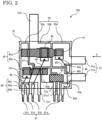
- FIG. 2 is a plan view showing an internal configuration of the semiconductor module 100.
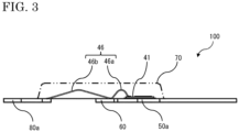
- FIG. 3 is a side view showing a major part of the internal configuration of the semiconductor module 100.
- a mold resin 70 is excluded, and the alternate long and two short dashes line indicates the external shape of the mold resin 70.
- FIG. 3 is a side view as seen in the direction of the arrow A shown in FIG. 2 .
- the semiconductor module 100 is a module that is used for a power conversion device or the like and that includes therein a plurality of semiconductor switching elements 41, 42, and 44 for performing power conversion.
- the electric power steering device 200 will be described as an example of the device including the semiconductor module 100.
- the electric power steering device 200 is a device that converts power supplied from a battery 9 and that outputs power obtained by the conversion to a motor 2.
- the electric power steering device 200 is composed of a control unit 1, the motor 2, the battery 9, an ignition switch 10, and sensors such as a rotation sensor 6.
- the motor 2 is a brushless motor composed of windings for three phases (a U phase, a V phase, and a W phase).
- the rotation sensor 6 is disposed near the motor 2, detects a rotation angle of the motor 2, and outputs the rotation angle to a control circuit 3 of the control unit 1.
- a sensor 8 includes a torque sensor for detecting steering wheel operation force, a vehicle speed sensor, and the like, and outputs an electric signal based on physical quantities detected by the respective sensors to the control circuit 3.
- the control unit 1 is composed of: the control circuit 3 including a CPU 30; an inverter circuit 4 for supplying current to the windings of the motor 2; a power supply relay 5; and other electrical components.
- the control unit 1 is connected to the battery 9 and the ignition switch 10, and power is supplied to the control unit 1 via the battery 9 and the ignition switch 10.
- the control unit 1 is connected to the rotation sensor 6 and the sensor 8, and electric signals outputted from these sensors are inputted to the control circuit 3 of the control unit 1.
- the control circuit 3 is composed of: the CPU 30; a drive circuit 31; an input circuit 32; and a power supply circuit 33 connected to these circuits. Output signals from the rotation sensor 6 and the sensor 8 are inputted to the input circuit 32, and data, obtained from these output signals, such as rotation angle information about the motor 2 are outputted to the CPU 30.
- the CPU 30 calculates, from the inputted data, a current value for rotating the motor 2.
- the CPU 30 outputs a control signal corresponding to the result obtained by the calculation, to the inverter circuit 4 via the drive circuit 31.
- a current detection signal detected by the inverter circuit 4 is inputted to the CPU 30 via the input circuit 32, and the CPU 30 performs feedback control on the inverter circuit 4 on the basis of the current detection signal.
- the inverter circuit 4 is composed of bridge circuits corresponding to respective windings for the three phases, i.e., the U phase, the V phase, and the W phase, of the motor 2. All of the bridge circuits corresponding to the respective phases are identical to one another, and thus a bridge circuit 4a for one phase (U phase) will be described.
- the bridge circuit 4a includes three semiconductor switching elements 41, 42, and 44.
- the semiconductor switching element 41 on a high-potential side and the semiconductor switching element 42 on a low-potential side are connected in series.
- One side of the semiconductor switching element 44 is connected to an intermediate connection portion between the semiconductor switching element 41 and the semiconductor switching element 42, and another side of the semiconductor switching element 44 is connected to a U-phase coil of the motor 2.
- the semiconductor switching element 44 has a relay function of enabling connection or disconnection between the U-phase coil and the inverter circuit 4.
- a shunt resistor 43 for detecting current is connected downstream of the semiconductor switching element 42 on the low-potential side. A potential difference between both ends of the shunt resistor 43 is detected and converted into a current value.
- terminals 48 are provided at both ends of the shunt resistor 43 in order to detect the potential difference between both ends of the shunt resistor 43.
- Monitor signals at various points of the inverter circuit 4 are inputted to the CPU 30 via the input circuit 32.
- Drive of the semiconductor switching elements 41, 42, and 44 is controlled on the basis of a signal outputted from the drive circuit 31 according to a command from the CPU 30.
- the power supply relay 5 is disposed upstream of the inverter circuit 4.
- the power supply relay 5 includes two semiconductor switching elements 5a and 5b connected in series.
- the power supply relay 5 has a relay function of enabling supply or interruption of power to the inverter circuit 4.
- Capacitors 7 for smoothing are connected in parallel between a ground and a power supply supplied to the inverter circuit 4.
- control unit 1 is configured by using a semiconductor module including therein a plurality of semiconductor switching elements
- semiconductor modules include: a semiconductor module including therein a bridge circuit composing the inverter circuit 4; a semiconductor module including therein the power supply relay 5; and a semiconductor module including therein a circuit obtained by eliminating some of the shunt resistors and the semiconductor switching elements.
- the semiconductor module 100 includes: base plates 50 each having the shape of a sheet; a relay plate 60 having the shape of a sheet; terminal members 80; and electronic components each joined to one surface of a corresponding one(s) of the base plates 50.
- the base plates 50, the relay plate 60, and the terminal members 80 are electrically conductive members made from a same material such as copper or a copper alloy.
- the base plates 50, the relay plate 60, and the terminal members 80 are provided side by side on a same plane with gaps between the electrically conductive members.
- five base plates 50 and four terminal members 80 are provided.
- the electronic components of the semiconductor module 100 are the semiconductor switching elements 41, 42, and 44 and the shunt resistor 43.
- the semiconductor switching elements 41, 42, and 44 described herein are field effect transistors (FETs). It is noted that the electronic components joined to the base plates 50 are not limited thereto.
- the semiconductor switching element 41 on the high-potential side is, at a drain portion of the semiconductor switching element 41, joined to one surface of a base plate 50a.
- the semiconductor switching element 42 on the low-potential side is, at a drain portion of the semiconductor switching element 42, joined to one surface of a base plate 50c.
- the semiconductor switching element 44 is, at a drain portion of the semiconductor switching element 44, joined to one surface of a base plate 50b.
- the shunt resistor 43 is joined on and between one surface of a base plate 50d and one surface of a base plate 50e.
- the semiconductor switching elements 41, 42, and 44 and base plates 50 are connected by, for example, jumper wires 45 each formed of a copper sheet and each having the shape of a bridge.
- a jumper wire 45a connects a source portion of the semiconductor switching element 41, a source portion of the semiconductor switching element 44, and the base plate 50c to each other.
- a jumper wire 45b connects a source portion of the semiconductor switching element 42 and the base plate 50d to each other.
- the base plates 50 include terminal portions 51 exposed to outside from side surfaces of the mold resin 70. Directions in which the terminal portions 51 are exposed are directions parallel to the same plane on which the base plates 50 are provided. A terminal portion 51a of the base plate 50a is connected to the battery 9 which is a power supply. A terminal portion 51e of the base plate 50e is connected to the ground. A terminal portion 51b of the base plate 50b is connected to the U phase of the motor 2 which is a load, and power obtained through conversion is outputted from the terminal portion 51b to the U phase of the motor 2.
- the terminal portions 51a, 51b, and 51e are high-current power terminals having large current amounts.
- the terminal portion 51a and the terminal portion 51e are disposed side by side on the right side of the semiconductor module 100.
- the terminal portion 51b is provided to extend in the upward direction from the semiconductor module 100.
- the base plate 50d and the base plate 50e respectively include a terminal portion 51d and a terminal portion 51e1 for detecting a voltage between both ends of the shunt resistor 43.
- the terminal portion 51e and the terminal portion 51e1 are each at the ground potential.
- the base plate 50c includes a terminal portion 51c connected to a connection point between the semiconductor switching elements 41, 42, and 44.
- the terminal portion 51c is a terminal for monitoring the potential of the connection point between the semiconductor switching elements 41, 42, and 44.
- Each terminal member 80 having the shape of a sheet includes a terminal portion 81 exposed to outside from a side surface of the mold resin 70.
- a direction in which the terminal portion 81 is exposed is a direction parallel to a same plane on which the terminal members 80 are provided.
- Each terminal member 80 is a terminal that has a relatively small current amount and that is used for controlling the semiconductor module 100.
- the terminal members 80 are disposed side by side on the lower side of the semiconductor module 100.
- Terminal members 80a, 80b, and 80c are gate control terminals connected to gate portions of the respective semiconductor switching elements 41, 42, and 44.
- Each of the terminal members 80a, 80b, and 80c and the corresponding gate portion are connected to each other by a bonding wire 46 provided in a wire bonding step.
- Each of the terminal members 80b and 80c and the corresponding gate portion are directly connected to each other by a bonding wire 46.
- the gate portion and one surface of the relay plate 60 are connected to each other by a bonding wire 46a
- the one surface of the relay plate 60 and one surface of the terminal member 80a are connected to each other by a bonding wire 46b.
- Wire bonding is performed from a start point which is the gate portion of each of the semiconductor switching elements 41, 42, and 44 to an end point which is a point on the corresponding terminal member 80 side.
- the bonding wires 46 can be cut without damaging the semiconductor switching elements 41, 42, and 44 in a wire bonding step.
- the gate portion of the semiconductor switching element 41 and the terminal member 80a are connected to each other via the relay plate 60, the start point and the end point are unchanged.
- a terminal member 80d and the base plate 50b are connected to each other by a bonding wire 47.
- the terminal member 80d is a terminal for monitoring the potential of the terminal portion 51b from which output to the motor 2 is performed.
- the mold resin 70 seals: the base plates 50; the relay plate 60; the terminal members 80; the semiconductor switching elements 41, 42, and 44 and the shunt resistor 43 which are electronic components; and the bonding wires 46 and 47.
- the mold resin 70 is formed in an external shape that is the shape of a rectangular sheet having a sheet surface parallel to the same plane on which the base plates 50 are provided. Another surface of each base plate 50 may be exposed from the mold resin 70 in order to easily cool the base plate 50.
- FIG. 5 is a diagram for explaining a semiconductor module 101 in the comparative example.
- FIG. 5(a) is a plan view showing a major part of the internal configuration of the semiconductor module 101.
- FIG. 5(b) is a side view showing the major part of the internal configuration of the semiconductor module 101.
- the base plate 50b and a relay plate 60a are connected to each other by a jumper wire 45c which is formed of a copper sheet and which has the shape of a bridge.
- the gate portion of the semiconductor switching element 41 and the terminal member 80a are connected to each other by a bonding wire 46c provided in a wire bonding step.
- Wire bonding between the gate portion and the terminal member 80a cannot be performed such that the bonding wire 46c extends over the jumper wire 45c.
- the bonding wire 46c is provided via, as a relay point, the jumper wire 45c on the relay plate 60a.
- the jumper wire 45c is at a higher position than one surface of each of the base plate 50a and the relay plate 60a, and thus the height of a loop of the bonding wire 46c increases at the positions indicated by the arrows in FIG. 5(b) . Since the height of the loop of the bonding wire 46c increases, the thickness of the mold resin 70 increases, whereby the semiconductor module 101 is upsized.
- the relay plate 60 which is a major part of the present disclosure will be described. As shown in FIG. 2 , the relay plate 60 has the shape of a rectangular sheet. If a direction parallel to a long side of the relay plate 60 is defined as a long side direction, each bonding wire 46 is connected to a one-side portion in the long side direction of the relay plate 60. If the relay plate 60 has the shape of a sheet, the relay plate 60 can be made from a material that is the same as the materials of the base plates 50 and can be disposed side by side with the base plates 50 on a plane that is the same as the plane of the base plates 50.
- the relay plate 60 can be disposed side by side with the base plates 50 on the plane that is the same as the plane of the base plates 50, the height of the loop of the bonding wire 46 connected to the relay plate 60 can be made low as shown in FIG. 3 . Since the height of the loop of the bonding wire 46 can be reduced, the thickness of the mold resin 70 is reduced, whereby the semiconductor module 101 can be downsized. If the relay plate 60 has a rectangular shape, the size thereof can be set such that the relay plate 60 only has an area necessary for wire bonding work. Therefore, the semiconductor module 100 can be downsized.
- the bonding wire 46 may be connected to an other-side portion in the long side direction. If the bonding wire 46 is connected to the one-side portion or the other-side portion in the long side direction of the relay plate 60, the other-side portion or the one-side portion to which the bonding wire 46 is not connected can be held down by using equipment such as a jig at the time of wire bonding work so as to fix the relay plate 60. Since the relay plate 60 can be easily fixed at the time of wire bonding work, productivity for the semiconductor module 100 can be improved.
- the semiconductor switching element 41 which is an electronic component is disposed on one side in the long side direction relative to the relay plate 60, the terminal member 80a is disposed on another side in the long side direction relative to the relay plate 60, and the bonding wire 46 is connected to the one-side portion in the long side direction of the relay plate 60.
- wire bonding work can be performed in the long side direction, and thus the productivity for the semiconductor module 100 can be improved.
- the length of the bonding wire 46 can be shortened.
- the semiconductor switching element 41 can be set as a start point for wire bonding, and the terminal member 80a can be set as an end point for the wire bonding, whereby the bonding wire 46 can be cut without damaging the semiconductor switching element 41.
- the bonding wire 46a connecting the semiconductor switching element 41 and the one surface of the relay plate 60 to each other, and the bonding wire 46b connecting the one surface of the relay plate 60 and the one surface of the terminal member 80a to each other, constitute a single bonding wire 46.
- the bonding wire 46a and the bonding wire 46b constitute a single bonding wire 46
- the semiconductor switching element 41 and the terminal member 80a can be connected to each other through continuous-wire bonding work without cutting the bonding wire 46 at an intermediate portion thereof. Consequently, the productivity for the semiconductor module 100 can be improved.
- the relay plate 60 is disposed such that one long side thereof extends along a side surface of the mold resin 70.
- a gap portion generated between the relay plate 60 and each base plate 50 can be reduced, whereby the semiconductor module 100 can be downsized.
- the degree of freedom in the layout of the base plates 50 can be improved.
- the size of each base plate 50 is ensured in the same manner as in a conventional configuration, and thus the heat dissipation property of the semiconductor module 100 can be maintained.
- the base plates 50, the relay plate 60, and the terminal members 80 are electrically conductive members and arranged on a same plane with gaps between the electrically conductive members, the semiconductor switching element 41 and the one surface of the relay plate 60 are connected to each other by the bonding wire 46a, and the one surface of the relay plate 60 and the one surface of the terminal member 80a are connected to each other by the bonding wire 46b. Consequently, bonding wire sagging and bonding wire sweep are inhibited, and furthermore, the thickness of the mold resin 70 which performs sealing for the semiconductor module 100 can be reduced.
- the size thereof can be set such that the relay plate 60 only has an area necessary for wire bonding work. Therefore, the semiconductor module 100 can be downsized.
- the other-side portion or the one-side portion to which the bonding wire 46 is not connected can be held down by using equipment such as a jig at the time of wire bonding work so as to easily fix the relay plate 60. Therefore, the productivity for the semiconductor module 100 can be improved.
- the semiconductor switching element 41 is disposed on the one side in the long side direction relative to the relay plate 60
- the terminal member 80a is disposed on the other side in the long side direction relative to the relay plate 60
- the bonding wire 46 is connected to the one-side portion in the long side direction of the relay plate 60
- wire bonding work can be performed in the long side direction, whereby the productivity for the semiconductor module 100 can be improved.
- the length of the bonding wire 46 can be shortened.
- the semiconductor switching element 41 can be set as a start point for wire bonding, and the terminal member 80a can be set as an end point for the wire bonding, whereby the bonding wire 46 can be cut without damaging the semiconductor switching element 41.
- the bonding wire 46a connecting the semiconductor switching element 41 and the one surface of the relay plate 60 to each other, and the bonding wire 46b connecting the one surface of the relay plate 60 and the one surface of the terminal member 80a to each other constitute a single bonding wire 46
- the semiconductor switching element 41 and the terminal member 80a can be connected to each other through continuous-wire bonding work without cutting the bonding wire 46 at an intermediate portion thereof. Consequently, the productivity for the semiconductor module 100 can be improved.
- the relay plate 60 is disposed such that one long side thereof extends along a side surface of the mold resin 70, a gap portion generated between the relay plate 60 and each base plate 50 can be reduced, whereby the semiconductor module 100 can be downsized.
- the degree of freedom in the layout of the base plates 50 can be improved.
- the size of each base plate 50 is ensured in the same manner as in a conventional configuration, and thus the heat dissipation property of the semiconductor module 100 can be maintained.
- the base plates 50, the relay plate 60, and the terminal members 80 are made from a same material
- the base plates 50, the relay plate 60, and the terminal members 80 can be made from a single sheet material without adding any separate member. Consequently, the productivity for the semiconductor module 100 can be improved.
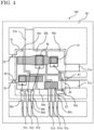
- FIG. 4 is a plan view showing an internal configuration of the semiconductor module 100 according to embodiment 2.
- the mold resin 70 is excluded, and the alternate long and two short dashes line indicates the external shape of the mold resin 70.
- the semiconductor module 100 according to embodiment 2 includes, in addition to the components described in embodiment 1, extending-out portions 52 and 61 exposed to outside from side surfaces of the mold resin 70.
- Each of the base plates 50, the relay plate 60, and the terminal members 80 includes a terminal portion 51, 81 or an extending-out portion 52, 61 exposed to outside from a side surface of the mold resin 70.
- Directions in which the terminal portions 51 and 81 and the extending-out portions 52 and 61 are exposed are directions parallel to the same plane on which the base plates 50 are provided.
- the terminal portions 51 and 81 and the extending-out portions 52 and 61 are connected to an outer frame 90 indicated by the broken lines in FIG. 4 at the time of manufacturing the semiconductor module 100.
- the base plates 50, the relay plate 60, the terminal members 80, and the outer frame 90 are formed of a single sheet material made from copper, a copper alloy, or the like.
- the semiconductor module 100 is manufactured in a state where the base plates 50, the relay plate 60, and the terminal members 80 are connected to the outer frame 90.
- a method for manufacturing the semiconductor module 100 includes: a step of punching an electrically conductive member having the shape of a sheet, to form a member in which the base plates 50, the relay plate 60, and the terminal members 80 are connected to the outer frame 90; a step of joining, to the base plate 50, the semiconductor switching elements 41, 42, and 44 and the shunt resistor 43 which are electronic components; a step of connecting the semiconductor switching elements 41, 42, and 44 and the base plates 50 by the jumper wires 45; a step of connecting the semiconductor switching elements 41, 42, and 44, the relay plate 60, and the terminal members 80 by the bonding wires 46 and 47; a step of sealing the base plates 50, the relay plate 60, the terminal members 80, the semiconductor switching elements 41, 42, and 44, the shunt resistor 43, and the bonding wires 46 and 47 by the mold resin 70; and a step of
- each of the base plates 50, the relay plate 60, and the terminal members 80 includes a terminal portion 51, 81 or an extending-out portion 52, 61 exposed to outside from a side surface of the mold resin 70, the arrangement of the base plates 50, the relay plate 60, and the terminal members 80 can be stabilized at the time of manufacturing the semiconductor module 100, without using another fixation member such as a jig. Since the arrangement of the base plates 50, the relay plate 60, and the terminal members 80 is stabilized, the productivity for the semiconductor module 100 can be improved.
- the extending-out portion 61 of the relay plate 60 will be described.
- the width of the extending-out portion 61 of the relay plate 60 is shorter than the length of the long side of the relay plate 60.
- the extending-out portion 61 can be easily cut off from the outer frame 90. Since the extending-out portion 61 can be easily cut off from the outer frame 90, the productivity for the semiconductor module 100 can be improved.
- the extending-out portion 61 of the relay plate 60 is provided on a side, on which there is the one long side of the relay plate 60, so as to be located at the other-side portion in the long side direction of the relay plate 60.
- the extending-out portion 61 is provided at the other-side portion, of the relay plate 60, to which the bonding wire 46 is not connected.
- the area of the relay plate 60 at a portion thereof on the side on which the bonding wire 46 is not connected is enlarged. Consequently, this portion can be easily held down by using equipment such as a jig at the time of wire bonding work so as to fix the relay plate 60.
- the relay plate 60 can be easily fixed at the time of wire bonding work, the productivity for the semiconductor module 100 can be improved.
- the relay plate 60, inclusive of the extending-out portion 61 can be held down by using equipment such as a jig. Consequently, the area of the relay plate 60 can be reduced, and the relay plate 60 can be downsized. Since the relay plate 60 can be downsized, the semiconductor module 100 can be downsized.
- each of the base plates 50, the relay plate 60, and the terminal members 80 includes a terminal portion 51, 81 or an extending-out portion 52, 61 exposed to outside from a side surface of the mold resin 70, and the directions in which the terminal portions 51 and 81 and the extending-out portions 52 and 61 are exposed are directions parallel to the same plane on which the base plates 50 are provided. Consequently, at the time of manufacturing, the terminal portions 51 and 81 and the extending-out portions 52 and 61 can be easily connected to the outer frame 90 which is to be cut off therefrom. Therefore, the arrangement of the base plates 50, the relay plate 60, and the terminal members 80 at the time of manufacturing the semiconductor module 100 can be stabilized. In addition, since the arrangement of the base plates 50, the relay plate 60, and the terminal members 80 is stabilized, the productivity for the semiconductor module 100 can be improved.
- the width of the extending-out portion 61 is set to be shorter than the length of the long side of the relay plate 60, the extending-out portion 61 can be easily cut off from the outer frame 90. Consequently, the productivity for the semiconductor module 100 can be improved.
- the extending-out portion 61 of the relay plate 60 is provided on a side, on which there is one long side of the relay plate 60, so as to be located at the one-side portion or the other-side portion, in the long side direction of the relay plate 60, which is on the side on which the bonding wire 46 is not connected, the area at the portion on the side on which the bonding wire 46 is not connected is enlarged.
- this portion can be easily held down by using equipment such as a jig at the time of wire bonding work so as to fix the relay plate 60. Since the relay plate 60 can be easily fixed at the time of wire bonding work, the productivity for the semiconductor module 100 can be improved.
- the relay plate 60 inclusive of the extending-out portion 61, can be held down by using equipment such as a jig, the relay plate 60 can be downsized. Since the relay plate 60 can be downsized, the semiconductor module 100 can be downsized.
Landscapes
- Engineering & Computer Science (AREA)
- Power Engineering (AREA)
- Inverter Devices (AREA)
- Structures Or Materials For Encapsulating Or Coating Semiconductor Devices Or Solid State Devices (AREA)
Abstract
Description
- The present disclosure relates to a semiconductor module.
- A semiconductor module including therein a semiconductor switching element is used for a power conversion device or the like. The semiconductor module is obtained by mounting a plurality of semiconductor switching elements on a base plate serving as an electrically conductive member, connecting, by means of jumper wires or bonding wires, electrode pads provided on the upper surfaces of the semiconductor switching elements, and then sealing these components with a mold resin. A plurality of terminal portions such as positive and negative power supply terminals, an output terminal for a load, and a control terminal for controlling each semiconductor switching element are arrayed on side surfaces on the outer periphery of the mold resin. In addition to the plurality of semiconductor switching elements, a shunt resistor for current detection and the like are also mounted inside the semiconductor module.
- If the length of a bonding wire provided inside the semiconductor module is excessively large, wire sagging, or wire sweep due to flow of the mold resin in a mold resin molding step, might occur. The occurrence of the wire sagging or the wire sweep leads to a problem that wire disconnection or short-circuiting due to contact between wires might occur. A three-dimensional wiring structure in which a relay wire member is disposed on a base plate, and a structure in which a relay for connection is performed via the relay wire member by means of wire bonding performed at a plurality of positions, have been disclosed to inhibit wire sagging and wire sweep (see, for example, Patent Document 1).
- Patent Document 1:
Japanese Laid-Open Patent Publication No. 2018-125424 - In an internal structure of a semiconductor module in the above Patent Document 1, bonding wires are connected via the relay wire member, in the three-dimensional wiring structure, which is disposed on the base plate. Consequently, wire sagging and wire sweep can be inhibited. However, since the wiring structure is three-dimensional, the height of a loop of the bonding wires is increased. Thus, the thickness of the mold resin is increased, resulting in a problem that the semiconductor module is upsized.
- Considering this, an object of the present disclosure is to provide a semiconductor module in which bonding wire sagging and bonding wire sweep are inhibited, and furthermore, the thickness of a mold resin which performs sealing for the semiconductor module is reduced.
- A semiconductor module according to the present disclosure includes: a base plate having a shape of a sheet; a relay plate having a shape of a sheet; a terminal member; and an electronic component joined to one surface of the base plate. The base plate, the relay plate, and the terminal member are electrically conductive members and arranged on a same plane with gaps between the electrically conductive members. The electronic component and one surface of the relay plate are connected to each other by a bonding wire. The one surface of the relay plate and one surface of the terminal member are connected to each other by a bonding wire.
- In the semiconductor module according to the present disclosure, the base plate, the relay plate, and the terminal member are electrically conductive members and arranged on the same plane with gaps between the electrically conductive members, the electronic component and the one surface of the relay plate are connected to each other by a bonding wire, and the one surface of the relay plate and the one surface of the terminal member are connected to each other by a bonding wire. Consequently, bonding wire sagging and bonding wire sweep can be inhibited, and furthermore, the thickness of a mold resin which performs sealing for the semiconductor module can be reduced.
-
- [
FIG. 1] FIG. 1 illustrates a circuit configuration of a device including a semiconductor module according to embodiment 1. - [
FIG. 2] FIG. 2 is a plan view showing the semiconductor module according to embodiment 1. - [
FIG. 3] FIG. 3 is a side view showing the semiconductor module according to embodiment 1. - [
FIG. 4] FIG. 4 is a plan view showing a semiconductor module according toembodiment 2. - [
FIG. 5] FIG. 5 is a diagram for explaining a semiconductor module in a comparative example. - Hereinafter, semiconductor modules according to embodiments of the present disclosure will be described with reference to the drawings. Description will be given while the same or corresponding members and parts in the drawings are denoted by the same reference characters.
-
FIG. 1 illustrates a circuit configuration of the entirety of a system of an electricpower steering device 200 including asemiconductor module 100 according to embodiment 1.FIG. 2 is a plan view showing an internal configuration of thesemiconductor module 100.FIG. 3 is a side view showing a major part of the internal configuration of thesemiconductor module 100. In each ofFIG. 2 andFIG. 3 , amold resin 70 is excluded, and the alternate long and two short dashes line indicates the external shape of themold resin 70.FIG. 3 is a side view as seen in the direction of the arrow A shown inFIG. 2 . Thesemiconductor module 100 is a module that is used for a power conversion device or the like and that includes therein a plurality ofsemiconductor switching elements - The electric
power steering device 200 will be described as an example of the device including thesemiconductor module 100. The electricpower steering device 200 is a device that converts power supplied from a battery 9 and that outputs power obtained by the conversion to amotor 2. As shown inFIG. 1 , the electricpower steering device 200 is composed of a control unit 1, themotor 2, the battery 9, anignition switch 10, and sensors such as arotation sensor 6. Themotor 2 is a brushless motor composed of windings for three phases (a U phase, a V phase, and a W phase). Therotation sensor 6 is disposed near themotor 2, detects a rotation angle of themotor 2, and outputs the rotation angle to a control circuit 3 of the control unit 1. Asensor 8 includes a torque sensor for detecting steering wheel operation force, a vehicle speed sensor, and the like, and outputs an electric signal based on physical quantities detected by the respective sensors to the control circuit 3. - The control unit 1 is composed of: the control circuit 3 including a
CPU 30; an inverter circuit 4 for supplying current to the windings of themotor 2; apower supply relay 5; and other electrical components. The control unit 1 is connected to the battery 9 and theignition switch 10, and power is supplied to the control unit 1 via the battery 9 and theignition switch 10. The control unit 1 is connected to therotation sensor 6 and thesensor 8, and electric signals outputted from these sensors are inputted to the control circuit 3 of the control unit 1. - The control circuit 3 is composed of: the
CPU 30; adrive circuit 31; aninput circuit 32; and a power supply circuit 33 connected to these circuits. Output signals from therotation sensor 6 and thesensor 8 are inputted to theinput circuit 32, and data, obtained from these output signals, such as rotation angle information about themotor 2 are outputted to theCPU 30. TheCPU 30 calculates, from the inputted data, a current value for rotating themotor 2. TheCPU 30 outputs a control signal corresponding to the result obtained by the calculation, to the inverter circuit 4 via thedrive circuit 31. In addition, a current detection signal detected by the inverter circuit 4 is inputted to theCPU 30 via theinput circuit 32, and theCPU 30 performs feedback control on the inverter circuit 4 on the basis of the current detection signal. - The inverter circuit 4 is composed of bridge circuits corresponding to respective windings for the three phases, i.e., the U phase, the V phase, and the W phase, of the
motor 2. All of the bridge circuits corresponding to the respective phases are identical to one another, and thus abridge circuit 4a for one phase (U phase) will be described. Thebridge circuit 4a includes threesemiconductor switching elements semiconductor switching element 41 on a high-potential side and thesemiconductor switching element 42 on a low-potential side are connected in series. One side of thesemiconductor switching element 44 is connected to an intermediate connection portion between thesemiconductor switching element 41 and thesemiconductor switching element 42, and another side of thesemiconductor switching element 44 is connected to a U-phase coil of themotor 2. Thesemiconductor switching element 44 has a relay function of enabling connection or disconnection between the U-phase coil and the inverter circuit 4. - A
shunt resistor 43 for detecting current is connected downstream of thesemiconductor switching element 42 on the low-potential side. A potential difference between both ends of theshunt resistor 43 is detected and converted into a current value. In the inverter circuit 4,terminals 48 are provided at both ends of theshunt resistor 43 in order to detect the potential difference between both ends of theshunt resistor 43. Monitor signals at various points of the inverter circuit 4 are inputted to theCPU 30 via theinput circuit 32. Drive of thesemiconductor switching elements drive circuit 31 according to a command from theCPU 30. - The
power supply relay 5 is disposed upstream of the inverter circuit 4. Thepower supply relay 5 includes twosemiconductor switching elements power supply relay 5 has a relay function of enabling supply or interruption of power to the inverter circuit 4.Capacitors 7 for smoothing are connected in parallel between a ground and a power supply supplied to the inverter circuit 4. - In the case where the control unit 1 is configured by using a semiconductor module including therein a plurality of semiconductor switching elements, various types of semiconductor modules are conceived. Examples of the semiconductor modules include: a semiconductor module including therein a bridge circuit composing the inverter circuit 4; a semiconductor module including therein the
power supply relay 5; and a semiconductor module including therein a circuit obtained by eliminating some of the shunt resistors and the semiconductor switching elements. - A case where the
bridge circuit 4a for the one phase is formed as asemiconductor module 100 will be described. As shown inFIG. 2 , thesemiconductor module 100 includes:base plates 50 each having the shape of a sheet; arelay plate 60 having the shape of a sheet;terminal members 80; and electronic components each joined to one surface of a corresponding one(s) of thebase plates 50. Thebase plates 50, therelay plate 60, and theterminal members 80 are electrically conductive members made from a same material such as copper or a copper alloy. Thebase plates 50, therelay plate 60, and theterminal members 80 are provided side by side on a same plane with gaps between the electrically conductive members. Here, fivebase plates 50 and fourterminal members 80 are provided. The electronic components of thesemiconductor module 100 are thesemiconductor switching elements shunt resistor 43. Thesemiconductor switching elements base plates 50 are not limited thereto. - The
semiconductor switching element 41 on the high-potential side is, at a drain portion of thesemiconductor switching element 41, joined to one surface of abase plate 50a. Thesemiconductor switching element 42 on the low-potential side is, at a drain portion of thesemiconductor switching element 42, joined to one surface of abase plate 50c. Thesemiconductor switching element 44 is, at a drain portion of thesemiconductor switching element 44, joined to one surface of abase plate 50b. Theshunt resistor 43 is joined on and between one surface of abase plate 50d and one surface of abase plate 50e. Thesemiconductor switching elements base plates 50 are connected by, for example,jumper wires 45 each formed of a copper sheet and each having the shape of a bridge. Ajumper wire 45a connects a source portion of thesemiconductor switching element 41, a source portion of thesemiconductor switching element 44, and thebase plate 50c to each other. Ajumper wire 45b connects a source portion of thesemiconductor switching element 42 and thebase plate 50d to each other. - The
base plates 50 includeterminal portions 51 exposed to outside from side surfaces of themold resin 70. Directions in which theterminal portions 51 are exposed are directions parallel to the same plane on which thebase plates 50 are provided. Aterminal portion 51a of thebase plate 50a is connected to the battery 9 which is a power supply. Aterminal portion 51e of thebase plate 50e is connected to the ground. Aterminal portion 51b of thebase plate 50b is connected to the U phase of themotor 2 which is a load, and power obtained through conversion is outputted from theterminal portion 51b to the U phase of themotor 2. Theterminal portions FIG. 2 , theterminal portion 51a and theterminal portion 51e are disposed side by side on the right side of thesemiconductor module 100. InFIG. 2 , theterminal portion 51b is provided to extend in the upward direction from thesemiconductor module 100. - The
base plate 50d and thebase plate 50e respectively include aterminal portion 51d and a terminal portion 51e1 for detecting a voltage between both ends of theshunt resistor 43. Theterminal portion 51e and the terminal portion 51e1 are each at the ground potential. Thebase plate 50c includes aterminal portion 51c connected to a connection point between thesemiconductor switching elements terminal portion 51c is a terminal for monitoring the potential of the connection point between thesemiconductor switching elements - Each
terminal member 80 having the shape of a sheet includes aterminal portion 81 exposed to outside from a side surface of themold resin 70. A direction in which theterminal portion 81 is exposed is a direction parallel to a same plane on which theterminal members 80 are provided. Eachterminal member 80 is a terminal that has a relatively small current amount and that is used for controlling thesemiconductor module 100. InFIG. 2 , theterminal members 80 are disposed side by side on the lower side of thesemiconductor module 100.Terminal members semiconductor switching elements terminal members bonding wire 46 provided in a wire bonding step. Each of theterminal members bonding wire 46. Regarding theterminal member 80a and the gate portion of thesemiconductor switching element 41, the gate portion and one surface of therelay plate 60 are connected to each other by abonding wire 46a, and the one surface of therelay plate 60 and one surface of theterminal member 80a are connected to each other by abonding wire 46b. By connecting theterminal member 80a and the gate portion to each other with division into thebonding wire 46a and thebonding wire 46b, the length of each bonding wire is shortened as compared to the case where theterminal member 80a and the gate portion are directly connected to each other by a single bonding wire. Consequently, bonding wire sagging and bonding wire sweep can be inhibited. - Wire bonding is performed from a start point which is the gate portion of each of the
semiconductor switching elements terminal member 80 side. Thus, thebonding wires 46 can be cut without damaging thesemiconductor switching elements semiconductor switching element 41 and theterminal member 80a are connected to each other via therelay plate 60, the start point and the end point are unchanged. Aterminal member 80d and thebase plate 50b are connected to each other by abonding wire 47. Theterminal member 80d is a terminal for monitoring the potential of theterminal portion 51b from which output to themotor 2 is performed. - The
mold resin 70 seals: thebase plates 50; therelay plate 60; theterminal members 80; thesemiconductor switching elements shunt resistor 43 which are electronic components; and thebonding wires mold resin 70 is formed in an external shape that is the shape of a rectangular sheet having a sheet surface parallel to the same plane on which thebase plates 50 are provided. Another surface of eachbase plate 50 may be exposed from themold resin 70 in order to easily cool thebase plate 50. - A comparative example will be described with reference to
FIG. 5 before therelay plate 60 which is a major part of the present disclosure is described.FIG. 5 is a diagram for explaining asemiconductor module 101 in the comparative example.FIG. 5(a) is a plan view showing a major part of the internal configuration of thesemiconductor module 101.FIG. 5(b) is a side view showing the major part of the internal configuration of thesemiconductor module 101. Thebase plate 50b and arelay plate 60a are connected to each other by ajumper wire 45c which is formed of a copper sheet and which has the shape of a bridge. The gate portion of thesemiconductor switching element 41 and theterminal member 80a are connected to each other by abonding wire 46c provided in a wire bonding step. Wire bonding between the gate portion and theterminal member 80a cannot be performed such that thebonding wire 46c extends over thejumper wire 45c. Thus, thebonding wire 46c is provided via, as a relay point, thejumper wire 45c on therelay plate 60a. Thejumper wire 45c is at a higher position than one surface of each of thebase plate 50a and therelay plate 60a, and thus the height of a loop of thebonding wire 46c increases at the positions indicated by the arrows inFIG. 5(b) . Since the height of the loop of thebonding wire 46c increases, the thickness of themold resin 70 increases, whereby thesemiconductor module 101 is upsized. - The
relay plate 60 which is a major part of the present disclosure will be described. As shown inFIG. 2 , therelay plate 60 has the shape of a rectangular sheet. If a direction parallel to a long side of therelay plate 60 is defined as a long side direction, eachbonding wire 46 is connected to a one-side portion in the long side direction of therelay plate 60. If therelay plate 60 has the shape of a sheet, therelay plate 60 can be made from a material that is the same as the materials of thebase plates 50 and can be disposed side by side with thebase plates 50 on a plane that is the same as the plane of thebase plates 50. Since therelay plate 60 can be disposed side by side with thebase plates 50 on the plane that is the same as the plane of thebase plates 50, the height of the loop of thebonding wire 46 connected to therelay plate 60 can be made low as shown inFIG. 3 . Since the height of the loop of thebonding wire 46 can be reduced, the thickness of themold resin 70 is reduced, whereby thesemiconductor module 101 can be downsized. If therelay plate 60 has a rectangular shape, the size thereof can be set such that therelay plate 60 only has an area necessary for wire bonding work. Therefore, thesemiconductor module 100 can be downsized. - Although the
bonding wire 46 is connected to the one-side portion in the long side direction herein, thebonding wire 46 may be connected to an other-side portion in the long side direction. If thebonding wire 46 is connected to the one-side portion or the other-side portion in the long side direction of therelay plate 60, the other-side portion or the one-side portion to which thebonding wire 46 is not connected can be held down by using equipment such as a jig at the time of wire bonding work so as to fix therelay plate 60. Since therelay plate 60 can be easily fixed at the time of wire bonding work, productivity for thesemiconductor module 100 can be improved. - The
semiconductor switching element 41 which is an electronic component is disposed on one side in the long side direction relative to therelay plate 60, theterminal member 80a is disposed on another side in the long side direction relative to therelay plate 60, and thebonding wire 46 is connected to the one-side portion in the long side direction of therelay plate 60. In the case of this arrangement, wire bonding work can be performed in the long side direction, and thus the productivity for thesemiconductor module 100 can be improved. In addition, the length of thebonding wire 46 can be shortened. In addition, thesemiconductor switching element 41 can be set as a start point for wire bonding, and theterminal member 80a can be set as an end point for the wire bonding, whereby thebonding wire 46 can be cut without damaging thesemiconductor switching element 41. - The
bonding wire 46a connecting thesemiconductor switching element 41 and the one surface of therelay plate 60 to each other, and thebonding wire 46b connecting the one surface of therelay plate 60 and the one surface of theterminal member 80a to each other, constitute asingle bonding wire 46. In the case where thebonding wire 46a and thebonding wire 46b constitute asingle bonding wire 46, thesemiconductor switching element 41 and theterminal member 80a can be connected to each other through continuous-wire bonding work without cutting thebonding wire 46 at an intermediate portion thereof. Consequently, the productivity for thesemiconductor module 100 can be improved. - The
relay plate 60 is disposed such that one long side thereof extends along a side surface of themold resin 70. In the case where therelay plate 60 is disposed along the side surface of themold resin 70 instead of being disposed at a position enclosed by thebase plates 50, a gap portion generated between therelay plate 60 and eachbase plate 50 can be reduced, whereby thesemiconductor module 100 can be downsized. In addition, the degree of freedom in the layout of thebase plates 50 can be improved. In addition, even though therelay plate 60 is provided, the size of eachbase plate 50 is ensured in the same manner as in a conventional configuration, and thus the heat dissipation property of thesemiconductor module 100 can be maintained. - As described above, in the
semiconductor module 100 according to embodiment 1, thebase plates 50, therelay plate 60, and theterminal members 80 are electrically conductive members and arranged on a same plane with gaps between the electrically conductive members, thesemiconductor switching element 41 and the one surface of therelay plate 60 are connected to each other by thebonding wire 46a, and the one surface of therelay plate 60 and the one surface of theterminal member 80a are connected to each other by thebonding wire 46b. Consequently, bonding wire sagging and bonding wire sweep are inhibited, and furthermore, the thickness of themold resin 70 which performs sealing for thesemiconductor module 100 can be reduced. In the case where therelay plate 60 has a rectangular shape, the size thereof can be set such that therelay plate 60 only has an area necessary for wire bonding work. Therefore, thesemiconductor module 100 can be downsized. - In the case where the
bonding wire 46 is connected to the one-side portion or the other-side portion in the long side direction of therelay plate 60, the other-side portion or the one-side portion to which thebonding wire 46 is not connected can be held down by using equipment such as a jig at the time of wire bonding work so as to easily fix therelay plate 60. Therefore, the productivity for thesemiconductor module 100 can be improved. In the case where thesemiconductor switching element 41 is disposed on the one side in the long side direction relative to therelay plate 60, theterminal member 80a is disposed on the other side in the long side direction relative to therelay plate 60, and thebonding wire 46 is connected to the one-side portion in the long side direction of therelay plate 60, wire bonding work can be performed in the long side direction, whereby the productivity for thesemiconductor module 100 can be improved. In addition, the length of thebonding wire 46 can be shortened. In addition, thesemiconductor switching element 41 can be set as a start point for wire bonding, and theterminal member 80a can be set as an end point for the wire bonding, whereby thebonding wire 46 can be cut without damaging thesemiconductor switching element 41. - In the case where the
bonding wire 46a connecting thesemiconductor switching element 41 and the one surface of therelay plate 60 to each other, and thebonding wire 46b connecting the one surface of therelay plate 60 and the one surface of theterminal member 80a to each other, constitute asingle bonding wire 46, thesemiconductor switching element 41 and theterminal member 80a can be connected to each other through continuous-wire bonding work without cutting thebonding wire 46 at an intermediate portion thereof. Consequently, the productivity for thesemiconductor module 100 can be improved. In the case where therelay plate 60 is disposed such that one long side thereof extends along a side surface of themold resin 70, a gap portion generated between therelay plate 60 and eachbase plate 50 can be reduced, whereby thesemiconductor module 100 can be downsized. In addition, the degree of freedom in the layout of thebase plates 50 can be improved. In addition, even though therelay plate 60 is provided, the size of eachbase plate 50 is ensured in the same manner as in a conventional configuration, and thus the heat dissipation property of thesemiconductor module 100 can be maintained. - In the case where the
base plates 50, therelay plate 60, and theterminal members 80 are made from a same material, thebase plates 50, therelay plate 60, and theterminal members 80 can be made from a single sheet material without adding any separate member. Consequently, the productivity for thesemiconductor module 100 can be improved. - A
semiconductor module 100 according toembodiment 2 will be described.FIG. 4 is a plan view showing an internal configuration of thesemiconductor module 100 according toembodiment 2. InFIG. 4 , themold resin 70 is excluded, and the alternate long and two short dashes line indicates the external shape of themold resin 70. Thesemiconductor module 100 according toembodiment 2 includes, in addition to the components described in embodiment 1, extending-outportions mold resin 70. - Each of the
base plates 50, therelay plate 60, and theterminal members 80 includes aterminal portion portion mold resin 70. Directions in which theterminal portions portions base plates 50 are provided. Theterminal portions portions outer frame 90 indicated by the broken lines inFIG. 4 at the time of manufacturing thesemiconductor module 100. Thebase plates 50, therelay plate 60, theterminal members 80, and theouter frame 90 are formed of a single sheet material made from copper, a copper alloy, or the like. - The
semiconductor module 100 is manufactured in a state where thebase plates 50, therelay plate 60, and theterminal members 80 are connected to theouter frame 90. A method for manufacturing thesemiconductor module 100 includes: a step of punching an electrically conductive member having the shape of a sheet, to form a member in which thebase plates 50, therelay plate 60, and theterminal members 80 are connected to theouter frame 90; a step of joining, to thebase plate 50, thesemiconductor switching elements shunt resistor 43 which are electronic components; a step of connecting thesemiconductor switching elements base plates 50 by thejumper wires 45; a step of connecting thesemiconductor switching elements relay plate 60, and theterminal members 80 by thebonding wires base plates 50, therelay plate 60, theterminal members 80, thesemiconductor switching elements shunt resistor 43, and thebonding wires mold resin 70; and a step of cutting off theouter frame 90 from theterminal portions portions - By cutting off the
outer frame 90 from theterminal portions portions semiconductor module 100 is completed. Since each of thebase plates 50, therelay plate 60, and theterminal members 80 includes aterminal portion portion mold resin 70, the arrangement of thebase plates 50, therelay plate 60, and theterminal members 80 can be stabilized at the time of manufacturing thesemiconductor module 100, without using another fixation member such as a jig. Since the arrangement of thebase plates 50, therelay plate 60, and theterminal members 80 is stabilized, the productivity for thesemiconductor module 100 can be improved. - The extending-out
portion 61 of therelay plate 60 will be described. The width of the extending-outportion 61 of therelay plate 60 is shorter than the length of the long side of therelay plate 60. In the case where the width of the extending-outportion 61 is set to be shorter than the length of the long side of therelay plate 60, the extending-outportion 61 can be easily cut off from theouter frame 90. Since the extending-outportion 61 can be easily cut off from theouter frame 90, the productivity for thesemiconductor module 100 can be improved. - The extending-out
portion 61 of therelay plate 60 is provided on a side, on which there is the one long side of therelay plate 60, so as to be located at the other-side portion in the long side direction of therelay plate 60. InFIG. 4 , the extending-outportion 61 is provided at the other-side portion, of therelay plate 60, to which thebonding wire 46 is not connected. In the case where the extending-outportion 61 is provided on the side on which thebonding wire 46 is not connected, the area of therelay plate 60 at a portion thereof on the side on which thebonding wire 46 is not connected is enlarged. Consequently, this portion can be easily held down by using equipment such as a jig at the time of wire bonding work so as to fix therelay plate 60. Since therelay plate 60 can be easily fixed at the time of wire bonding work, the productivity for thesemiconductor module 100 can be improved. In addition, therelay plate 60, inclusive of the extending-outportion 61, can be held down by using equipment such as a jig. Consequently, the area of therelay plate 60 can be reduced, and therelay plate 60 can be downsized. Since therelay plate 60 can be downsized, thesemiconductor module 100 can be downsized. - As described above, in the
semiconductor module 100 according toembodiment 2, each of thebase plates 50, therelay plate 60, and theterminal members 80 includes aterminal portion portion mold resin 70, and the directions in which theterminal portions portions base plates 50 are provided. Consequently, at the time of manufacturing, theterminal portions portions outer frame 90 which is to be cut off therefrom. Therefore, the arrangement of thebase plates 50, therelay plate 60, and theterminal members 80 at the time of manufacturing thesemiconductor module 100 can be stabilized. In addition, since the arrangement of thebase plates 50, therelay plate 60, and theterminal members 80 is stabilized, the productivity for thesemiconductor module 100 can be improved. - In the case where the width of the extending-out
portion 61 is set to be shorter than the length of the long side of therelay plate 60, the extending-outportion 61 can be easily cut off from theouter frame 90. Consequently, the productivity for thesemiconductor module 100 can be improved. In the case where the extending-outportion 61 of therelay plate 60 is provided on a side, on which there is one long side of therelay plate 60, so as to be located at the one-side portion or the other-side portion, in the long side direction of therelay plate 60, which is on the side on which thebonding wire 46 is not connected, the area at the portion on the side on which thebonding wire 46 is not connected is enlarged. Consequently, this portion can be easily held down by using equipment such as a jig at the time of wire bonding work so as to fix therelay plate 60. Since therelay plate 60 can be easily fixed at the time of wire bonding work, the productivity for thesemiconductor module 100 can be improved. In addition, since therelay plate 60, inclusive of the extending-outportion 61, can be held down by using equipment such as a jig, therelay plate 60 can be downsized. Since therelay plate 60 can be downsized, thesemiconductor module 100 can be downsized. - Although the disclosure is described above in terms of various exemplary embodiments and implementations, it should be understood that the various features, aspects, and functionality described in one or more of the individual embodiments are not limited in their applicability to the particular embodiment with which they are described, but instead can be applied, alone or in various combinations to one or more of the embodiments of the disclosure.
- It is therefore understood that numerous modifications which have not been exemplified can be devised without departing from the scope of the specification of the present disclosure. For example, at least one of the constituent components may be modified, added, or eliminated. At least one of the constituent components mentioned in at least one of the preferred embodiments may be selected and combined with the constituent components mentioned in another preferred embodiment.
-
- 1
- control unit
- 2
- motor
- 3
- control circuit
- 4
- inverter circuit
- 4a
- bridge circuit
- 5
- power supply relay
- 5a
- semiconductor switching element
- 5b
- semiconductor switching element
- 6
- rotation sensor
- 7
- capacitor
- 8
- sensor
- 9
- battery
- 10
- ignition switch
- 30
- CPU
- 31
- drive circuit
- 32
- input circuit
- 33
- power supply circuit
- 41
- semiconductor switching element
- 42
- semiconductor switching element
- 43
- shunt resistor
- 44
- semiconductor switching element
- 45
- jumper wire
- 46
- bonding wire
- 47
- bonding wire
- 48
- terminal
- 50
- base plate
- 51
- terminal portion
- 52
- extending-out portion
- 60
- relay plate
- 60a
- relay plate
- 61
- extending-out portion
- 70
- mold resin
- 80
- terminal member
- 81
- terminal portion
- 90
- outer frame
- 100
- semiconductor module
- 101
- semiconductor module
- 200
- electric power steering device
Claims (8)
- A semiconductor module comprising:a base plate having a shape of a sheet;a relay plate having a shape of a sheet;a terminal member; andan electronic component joined to one surface of the base plate, whereinthe base plate, the relay plate, and the terminal member are electrically conductive members and arranged on a same plane with gaps between the electrically conductive members,the electronic component and one surface of the relay plate are connected to each other by a bonding wire, andthe one surface of the relay plate and one surface of the terminal member are connected to each other by a bonding wire.
- The semiconductor module according to claim 1, whereinthe relay plate has a shape of a rectangular sheet, and,if a direction parallel to a long side of the relay plate is defined as a long side direction, each bonding wire is connected to a one-side portion or an other-side portion in the long side direction of the relay plate.
- The semiconductor module according to claim 2, whereinthe electronic component is disposed on one side in the long side direction relative to the relay plate,the terminal member is disposed on another side in the long side direction relative to the relay plate, andthe bonding wire is connected to the one-side portion in the long side direction of the relay plate.
- The semiconductor module according to claim 3, wherein the bonding wire connecting the electronic component and the one surface of the relay plate to each other, and the bonding wire connecting the one surface of the relay plate and the one surface of the terminal member to each other, constitute a single bonding wire.
- The semiconductor module according to claim 2, further comprisinga mold resin sealing the base plate, the relay plate, the terminal member, the electronic component, and the bonding wire, whereinthe mold resin is formed in an external shape that is a shape of a rectangular sheet having a sheet surface parallel to the same plane, andthe relay plate is disposed such that one long side thereof extends along a side surface of the mold resin.
- The semiconductor module according to claim 2, wherein the base plate, the relay plate, and the terminal member are made from a same material.
- The semiconductor module according to claim 5, whereineach of the base plate, the relay plate, and the terminal member includes a terminal portion or an extending-out portion exposed to outside from a side surface of the mold resin, anddirections in which the terminal portion and the extending-out portion are exposed are directions parallel to the same plane.
- The semiconductor module according to claim 7, whereina width of the extending-out portion of the relay plate is shorter than a length of the long side of the relay plate, andthe extending-out portion of the relay plate is provided on a side, on which there is one long side of the relay plate, so as to be located at the one-side portion or the other-side portion in the long side direction of the relay plate.
Applications Claiming Priority (1)
| Application Number | Priority Date | Filing Date | Title |
|---|---|---|---|
| PCT/JP2020/019718 WO2021234803A1 (en) | 2020-05-19 | 2020-05-19 | Semiconductor module |
Publications (3)
| Publication Number | Publication Date |
|---|---|
| EP4156252A1 true EP4156252A1 (en) | 2023-03-29 |
| EP4156252A4 EP4156252A4 (en) | 2023-08-09 |
| EP4156252B1 EP4156252B1 (en) | 2026-01-28 |
Family
ID=78708417
Family Applications (1)
| Application Number | Title | Priority Date | Filing Date |
|---|---|---|---|
| EP20936107.0A Active EP4156252B1 (en) | 2020-05-19 | 2020-05-19 | Semiconductor module and method of manufacturing semiconductor module |
Country Status (5)
| Country | Link |
|---|---|
| US (1) | US12412813B2 (en) |
| EP (1) | EP4156252B1 (en) |
| JP (1) | JP7214050B2 (en) |
| CN (1) | CN115552597A (en) |
| WO (1) | WO2021234803A1 (en) |
Families Citing this family (1)
| Publication number | Priority date | Publication date | Assignee | Title |
|---|---|---|---|---|
| US20250286492A1 (en) * | 2024-03-07 | 2025-09-11 | BorgWarner US Technologies LLC | Systems for power module assembly for inverter |
Family Cites Families (12)
| Publication number | Priority date | Publication date | Assignee | Title |
|---|---|---|---|---|
| JPH07101726B2 (en) * | 1985-08-13 | 1995-11-01 | 松下電子工業株式会社 | Lead frame |
| JPH02177354A (en) * | 1988-12-27 | 1990-07-10 | Matsushita Electric Ind Co Ltd | Semiconductor element |
| CN102254839B (en) * | 2010-05-21 | 2015-09-02 | 刘圣平 | The outer simple and easy integrated approach of a kind of ic core and framework |
| US10211134B2 (en) | 2011-09-30 | 2019-02-19 | Mediatek Inc. | Semiconductor package |
| CN102790513B (en) * | 2012-07-30 | 2014-12-10 | 华为技术有限公司 | Power supply module and packaging method thereof |
| JP6094420B2 (en) * | 2013-08-09 | 2017-03-15 | 三菱電機株式会社 | Semiconductor device |
| EP4220708A1 (en) * | 2013-11-20 | 2023-08-02 | Rohm Co., Ltd. | Switching device and electronic circuit |
| JP2015228447A (en) * | 2014-06-02 | 2015-12-17 | 株式会社デンソー | Semiconductor device manufacturing method |
| JP2016174055A (en) * | 2015-03-16 | 2016-09-29 | 株式会社東芝 | Semiconductor device |
| JP6520437B2 (en) * | 2015-06-12 | 2019-05-29 | 富士電機株式会社 | Semiconductor device |
| JP2018125424A (en) | 2017-02-01 | 2018-08-09 | 日本精工株式会社 | Semiconductor module, control unit equipped with the module, and electric power steering system |
| JP6729474B2 (en) | 2017-04-24 | 2020-07-22 | 三菱電機株式会社 | Semiconductor device |
-
2020
- 2020-05-19 US US17/794,870 patent/US12412813B2/en active Active
- 2020-05-19 CN CN202080100643.7A patent/CN115552597A/en not_active Withdrawn
- 2020-05-19 EP EP20936107.0A patent/EP4156252B1/en active Active
- 2020-05-19 JP JP2022523782A patent/JP7214050B2/en active Active
- 2020-05-19 WO PCT/JP2020/019718 patent/WO2021234803A1/en not_active Ceased
Also Published As
| Publication number | Publication date |
|---|---|
| CN115552597A (en) | 2022-12-30 |
| US20230096581A1 (en) | 2023-03-30 |
| EP4156252B1 (en) | 2026-01-28 |
| WO2021234803A1 (en) | 2021-11-25 |
| JP7214050B2 (en) | 2023-01-27 |
| JPWO2021234803A1 (en) | 2021-11-25 |
| US12412813B2 (en) | 2025-09-09 |
| EP4156252A4 (en) | 2023-08-09 |
Similar Documents
| Publication | Publication Date | Title |
|---|---|---|
| US10556618B2 (en) | Drive apparatus and electric power steering apparatus using the same | |
| US10897219B2 (en) | Drive apparatus and electric power steering apparatus using the same | |
| US10479398B2 (en) | Integrated electric power steering apparatus and manufacturing method therefor | |
| US8564996B2 (en) | Semiconductor module and driving apparatus including semiconductor module | |
| CN102810532B (en) | Semiconductor device and the driving equipment including semiconductor device | |
| CN105406652A (en) | Power Conversion Device | |
| JP2020009865A (en) | Power module | |
| EP4156252B1 (en) | Semiconductor module and method of manufacturing semiconductor module | |
| US11626347B2 (en) | Shared base plate and semiconductor module provided with same | |
| JP6794841B2 (en) | Power converter and its manufacturing method | |
| EP4415040A1 (en) | Semiconductor module and method for manufacturing same | |
| JP5407244B2 (en) | Motor drive device | |
| JP2006197735A (en) | Inverter | |
| EP4227987A1 (en) | Semiconductor module | |
| JP2013140889A (en) | Power module | |
| CN106415831B (en) | Semiconductor module |
Legal Events
| Date | Code | Title | Description |
|---|---|---|---|
| STAA | Information on the status of an ep patent application or granted ep patent |
Free format text: STATUS: THE INTERNATIONAL PUBLICATION HAS BEEN MADE |
|
| PUAI | Public reference made under article 153(3) epc to a published international application that has entered the european phase |
Free format text: ORIGINAL CODE: 0009012 |
|
| STAA | Information on the status of an ep patent application or granted ep patent |
Free format text: STATUS: REQUEST FOR EXAMINATION WAS MADE |
|
| 17P | Request for examination filed |
Effective date: 20220714 |
|
| AK | Designated contracting states |
Kind code of ref document: A1 Designated state(s): AL AT BE BG CH CY CZ DE DK EE ES FI FR GB GR HR HU IE IS IT LI LT LU LV MC MK MT NL NO PL PT RO RS SE SI SK SM TR |
|
| A4 | Supplementary search report drawn up and despatched |
Effective date: 20230710 |
|
| RIC1 | Information provided on ipc code assigned before grant |
Ipc: H02M 7/00 20060101ALI20230704BHEP Ipc: H01L 23/495 20060101ALI20230704BHEP Ipc: H01L 25/18 20230101ALI20230704BHEP Ipc: H01L 25/07 20060101ALI20230704BHEP Ipc: H01L 23/48 20060101AFI20230704BHEP |
|
| DAV | Request for validation of the european patent (deleted) | ||
| DAX | Request for extension of the european patent (deleted) | ||
| GRAJ | Information related to disapproval of communication of intention to grant by the applicant or resumption of examination proceedings by the epo deleted |
Free format text: ORIGINAL CODE: EPIDOSDIGR1 |
|
| GRAP | Despatch of communication of intention to grant a patent |
Free format text: ORIGINAL CODE: EPIDOSNIGR1 |
|
| GRAP | Despatch of communication of intention to grant a patent |
Free format text: ORIGINAL CODE: EPIDOSNIGR1 |
|
| STAA | Information on the status of an ep patent application or granted ep patent |
Free format text: STATUS: GRANT OF PATENT IS INTENDED |
|
| INTG | Intention to grant announced |
Effective date: 20251017 |
|
| GRAS | Grant fee paid |
Free format text: ORIGINAL CODE: EPIDOSNIGR3 |
|
| GRAA | (expected) grant |
Free format text: ORIGINAL CODE: 0009210 |
|
| STAA | Information on the status of an ep patent application or granted ep patent |
Free format text: STATUS: THE PATENT HAS BEEN GRANTED |
|
| AK | Designated contracting states |
Kind code of ref document: B1 Designated state(s): AL AT BE BG CH CY CZ DE DK EE ES FI FR GB GR HR HU IE IS IT LI LT LU LV MC MK MT NL NO PL PT RO RS SE SI SK SM TR |
|
| REG | Reference to a national code |
Ref country code: CH Ref legal event code: F10 Free format text: ST27 STATUS EVENT CODE: U-0-0-F10-F00 (AS PROVIDED BY THE NATIONAL OFFICE) Effective date: 20260128 Ref country code: GB Ref legal event code: FG4D |
|
| REG | Reference to a national code |
Ref country code: DE Ref legal event code: R096 Ref document number: 602020066397 Country of ref document: DE |
|
| REG | Reference to a national code |
Ref country code: IE Ref legal event code: FG4D |