EP4155663A1 - Electronic device - Google Patents
Electronic device Download PDFInfo
- Publication number
- EP4155663A1 EP4155663A1 EP21808067.9A EP21808067A EP4155663A1 EP 4155663 A1 EP4155663 A1 EP 4155663A1 EP 21808067 A EP21808067 A EP 21808067A EP 4155663 A1 EP4155663 A1 EP 4155663A1
- Authority
- EP
- European Patent Office
- Prior art keywords
- light
- substrate
- shielding
- electronic device
- drive circuit
- Prior art date
- Legal status (The legal status is an assumption and is not a legal conclusion. Google has not performed a legal analysis and makes no representation as to the accuracy of the status listed.)
- Pending
Links
- 239000000758 substrate Substances 0.000 claims abstract description 172
- 230000002093 peripheral effect Effects 0.000 claims description 38
- 230000001681 protective effect Effects 0.000 claims description 27
- 239000000463 material Substances 0.000 claims description 17
- 230000007257 malfunction Effects 0.000 abstract description 21
- 239000010410 layer Substances 0.000 description 71
- 229920005989 resin Polymers 0.000 description 35
- 239000011347 resin Substances 0.000 description 35
- 238000012986 modification Methods 0.000 description 32
- 230000004048 modification Effects 0.000 description 32
- VYPSYNLAJGMNEJ-UHFFFAOYSA-N Silicium dioxide Chemical compound O=[Si]=O VYPSYNLAJGMNEJ-UHFFFAOYSA-N 0.000 description 20
- 238000012937 correction Methods 0.000 description 17
- 230000000694 effects Effects 0.000 description 15
- 230000003287 optical effect Effects 0.000 description 12
- 229910052751 metal Inorganic materials 0.000 description 11
- 239000002184 metal Substances 0.000 description 11
- 238000012545 processing Methods 0.000 description 11
- 239000010949 copper Substances 0.000 description 10
- 229910052681 coesite Inorganic materials 0.000 description 9
- 229910052906 cristobalite Inorganic materials 0.000 description 9
- 239000000377 silicon dioxide Substances 0.000 description 9
- 229910052682 stishovite Inorganic materials 0.000 description 9
- 229910052905 tridymite Inorganic materials 0.000 description 9
- 238000003384 imaging method Methods 0.000 description 8
- 229910052782 aluminium Inorganic materials 0.000 description 7
- XAGFODPZIPBFFR-UHFFFAOYSA-N aluminium Chemical compound [Al] XAGFODPZIPBFFR-UHFFFAOYSA-N 0.000 description 7
- 238000010586 diagram Methods 0.000 description 7
- 230000017525 heat dissipation Effects 0.000 description 6
- RYGMFSIKBFXOCR-UHFFFAOYSA-N Copper Chemical compound [Cu] RYGMFSIKBFXOCR-UHFFFAOYSA-N 0.000 description 5
- 229910052802 copper Inorganic materials 0.000 description 5
- 238000002955 isolation Methods 0.000 description 5
- PCHJSUWPFVWCPO-UHFFFAOYSA-N gold Chemical compound [Au] PCHJSUWPFVWCPO-UHFFFAOYSA-N 0.000 description 4
- 239000010931 gold Substances 0.000 description 4
- 238000004519 manufacturing process Methods 0.000 description 4
- 238000000034 method Methods 0.000 description 4
- 239000004065 semiconductor Substances 0.000 description 4
- PXHVJJICTQNCMI-UHFFFAOYSA-N Nickel Chemical compound [Ni] PXHVJJICTQNCMI-UHFFFAOYSA-N 0.000 description 3
- 238000005229 chemical vapour deposition Methods 0.000 description 3
- 239000011229 interlayer Substances 0.000 description 3
- 230000001902 propagating effect Effects 0.000 description 3
- 239000010936 titanium Substances 0.000 description 3
- 229910052581 Si3N4 Inorganic materials 0.000 description 2
- NRTOMJZYCJJWKI-UHFFFAOYSA-N Titanium nitride Chemical compound [Ti]#N NRTOMJZYCJJWKI-UHFFFAOYSA-N 0.000 description 2
- 230000002238 attenuated effect Effects 0.000 description 2
- 238000006243 chemical reaction Methods 0.000 description 2
- 230000006870 function Effects 0.000 description 2
- 229910052737 gold Inorganic materials 0.000 description 2
- 239000011159 matrix material Substances 0.000 description 2
- 238000000059 patterning Methods 0.000 description 2
- 238000000206 photolithography Methods 0.000 description 2
- HQVNEWCFYHHQES-UHFFFAOYSA-N silicon nitride Chemical compound N12[Si]34N5[Si]62N3[Si]51N64 HQVNEWCFYHHQES-UHFFFAOYSA-N 0.000 description 2
- 229910052814 silicon oxide Inorganic materials 0.000 description 2
- 238000004544 sputter deposition Methods 0.000 description 2
- 229910000838 Al alloy Inorganic materials 0.000 description 1
- PIGFYZPCRLYGLF-UHFFFAOYSA-N Aluminum nitride Chemical compound [Al]#N PIGFYZPCRLYGLF-UHFFFAOYSA-N 0.000 description 1
- RTAQQCXQSZGOHL-UHFFFAOYSA-N Titanium Chemical compound [Ti] RTAQQCXQSZGOHL-UHFFFAOYSA-N 0.000 description 1
- 239000000919 ceramic Substances 0.000 description 1
- 230000000295 complement effect Effects 0.000 description 1
- 230000001276 controlling effect Effects 0.000 description 1
- 230000002596 correlated effect Effects 0.000 description 1
- 230000000875 corresponding effect Effects 0.000 description 1
- 238000005520 cutting process Methods 0.000 description 1
- 238000005516 engineering process Methods 0.000 description 1
- 239000003822 epoxy resin Substances 0.000 description 1
- 238000005530 etching Methods 0.000 description 1
- 239000012535 impurity Substances 0.000 description 1
- 230000001678 irradiating effect Effects 0.000 description 1
- 239000007769 metal material Substances 0.000 description 1
- 239000000203 mixture Substances 0.000 description 1
- 238000000465 moulding Methods 0.000 description 1
- 229910052759 nickel Inorganic materials 0.000 description 1
- 230000001151 other effect Effects 0.000 description 1
- 230000000149 penetrating effect Effects 0.000 description 1
- 229920002120 photoresistant polymer Polymers 0.000 description 1
- 238000005498 polishing Methods 0.000 description 1
- 229910021420 polycrystalline silicon Inorganic materials 0.000 description 1
- 229920000647 polyepoxide Polymers 0.000 description 1
- 229920005591 polysilicon Polymers 0.000 description 1
- 230000035945 sensitivity Effects 0.000 description 1
- 239000000126 substance Substances 0.000 description 1
- 238000006467 substitution reaction Methods 0.000 description 1
- 229910052719 titanium Inorganic materials 0.000 description 1
- 238000013519 translation Methods 0.000 description 1
Images










Classifications
-
- H—ELECTRICITY
- H01—ELECTRIC ELEMENTS
- H01S—DEVICES USING THE PROCESS OF LIGHT AMPLIFICATION BY STIMULATED EMISSION OF RADIATION [LASER] TO AMPLIFY OR GENERATE LIGHT; DEVICES USING STIMULATED EMISSION OF ELECTROMAGNETIC RADIATION IN WAVE RANGES OTHER THAN OPTICAL
- H01S5/00—Semiconductor lasers
- H01S5/02—Structural details or components not essential to laser action
- H01S5/028—Coatings ; Treatment of the laser facets, e.g. etching, passivation layers or reflecting layers
-
- H—ELECTRICITY
- H01—ELECTRIC ELEMENTS
- H01S—DEVICES USING THE PROCESS OF LIGHT AMPLIFICATION BY STIMULATED EMISSION OF RADIATION [LASER] TO AMPLIFY OR GENERATE LIGHT; DEVICES USING STIMULATED EMISSION OF ELECTROMAGNETIC RADIATION IN WAVE RANGES OTHER THAN OPTICAL
- H01S5/00—Semiconductor lasers
- H01S5/02—Structural details or components not essential to laser action
- H01S5/022—Mountings; Housings
- H01S5/0239—Combinations of electrical or optical elements
-
- H—ELECTRICITY
- H01—ELECTRIC ELEMENTS
- H01S—DEVICES USING THE PROCESS OF LIGHT AMPLIFICATION BY STIMULATED EMISSION OF RADIATION [LASER] TO AMPLIFY OR GENERATE LIGHT; DEVICES USING STIMULATED EMISSION OF ELECTROMAGNETIC RADIATION IN WAVE RANGES OTHER THAN OPTICAL
- H01S5/00—Semiconductor lasers
- H01S5/04—Processes or apparatus for excitation, e.g. pumping, e.g. by electron beams
- H01S5/042—Electrical excitation ; Circuits therefor
-
- H—ELECTRICITY
- H01—ELECTRIC ELEMENTS
- H01S—DEVICES USING THE PROCESS OF LIGHT AMPLIFICATION BY STIMULATED EMISSION OF RADIATION [LASER] TO AMPLIFY OR GENERATE LIGHT; DEVICES USING STIMULATED EMISSION OF ELECTROMAGNETIC RADIATION IN WAVE RANGES OTHER THAN OPTICAL
- H01S5/00—Semiconductor lasers
- H01S5/40—Arrangement of two or more semiconductor lasers, not provided for in groups H01S5/02 - H01S5/30
- H01S5/42—Arrays of surface emitting lasers
- H01S5/423—Arrays of surface emitting lasers having a vertical cavity
-
- H—ELECTRICITY
- H01—ELECTRIC ELEMENTS
- H01S—DEVICES USING THE PROCESS OF LIGHT AMPLIFICATION BY STIMULATED EMISSION OF RADIATION [LASER] TO AMPLIFY OR GENERATE LIGHT; DEVICES USING STIMULATED EMISSION OF ELECTROMAGNETIC RADIATION IN WAVE RANGES OTHER THAN OPTICAL
- H01S5/00—Semiconductor lasers
- H01S5/02—Structural details or components not essential to laser action
- H01S5/022—Mountings; Housings
- H01S5/0225—Out-coupling of light
- H01S5/02253—Out-coupling of light using lenses
-
- H—ELECTRICITY
- H01—ELECTRIC ELEMENTS
- H01S—DEVICES USING THE PROCESS OF LIGHT AMPLIFICATION BY STIMULATED EMISSION OF RADIATION [LASER] TO AMPLIFY OR GENERATE LIGHT; DEVICES USING STIMULATED EMISSION OF ELECTROMAGNETIC RADIATION IN WAVE RANGES OTHER THAN OPTICAL
- H01S5/00—Semiconductor lasers
- H01S5/02—Structural details or components not essential to laser action
- H01S5/022—Mountings; Housings
- H01S5/0233—Mounting configuration of laser chips
- H01S5/0234—Up-side down mountings, e.g. Flip-chip, epi-side down mountings or junction down mountings
-
- H—ELECTRICITY
- H01—ELECTRIC ELEMENTS
- H01S—DEVICES USING THE PROCESS OF LIGHT AMPLIFICATION BY STIMULATED EMISSION OF RADIATION [LASER] TO AMPLIFY OR GENERATE LIGHT; DEVICES USING STIMULATED EMISSION OF ELECTROMAGNETIC RADIATION IN WAVE RANGES OTHER THAN OPTICAL
- H01S5/00—Semiconductor lasers
- H01S5/06—Arrangements for controlling the laser output parameters, e.g. by operating on the active medium
- H01S5/068—Stabilisation of laser output parameters
- H01S5/06804—Stabilisation of laser output parameters by monitoring an external parameter, e.g. temperature
-
- H—ELECTRICITY
- H01—ELECTRIC ELEMENTS
- H01S—DEVICES USING THE PROCESS OF LIGHT AMPLIFICATION BY STIMULATED EMISSION OF RADIATION [LASER] TO AMPLIFY OR GENERATE LIGHT; DEVICES USING STIMULATED EMISSION OF ELECTROMAGNETIC RADIATION IN WAVE RANGES OTHER THAN OPTICAL
- H01S5/00—Semiconductor lasers
- H01S5/10—Construction or shape of the optical resonator, e.g. extended or external cavity, coupled cavities, bent-guide, varying width, thickness or composition of the active region
- H01S5/18—Surface-emitting [SE] lasers, e.g. having both horizontal and vertical cavities
- H01S5/183—Surface-emitting [SE] lasers, e.g. having both horizontal and vertical cavities having only vertical cavities, e.g. vertical cavity surface-emitting lasers [VCSEL]
Definitions
- the present disclosure relates to an electronic device.
- a surface-emitting laser such as a vertical-cavity surface-emitting laser (VCSEL) is known (e.g., see Patent Documents 1 and 2.).
- VCSEL vertical-cavity surface-emitting laser
- a plurality of light-emitting elements is provided in a two-dimensional array on the front surface or back surface of a substrate, and a lens is disposed thereon. The light emitted from the plurality of light-emitting elements is emitted to the outside of the light-emitting device through the lens.
- Fig. 7A of Patent Document 2 discloses a configuration in which a chip having a circuit as a light-emitting unit formed therein is flip chip-mounted on a chip in which a circuit as a drive unit is formed.
- the drive unit has elements (e.g., bipolar transistors) each including a p-n junction surface. When light strikes these elements, a photovoltaic effect occurs, the characteristics of the elements change, and there is a possibility that the drive unit malfunctions.
- the present disclosure has been made in view of such circumstances, and an object of the present disclosure is to provide an electronic device capable of reducing the possibility of malfunction.
- An electronic device is provided with: a first substrate including a drive circuit; a second substrate including a light-emitting unit driven by the drive circuit and mounted on one surface side of the first substrate; and a light-shielding unit provided on the first substrate and configured to shield at least a part of the drive circuit from light emitted by the light-emitting unit.
- the light-shielding unit can reduce the occurrence of a photovoltaic effect on a p-n junction surface of an element (e.g., bipolar transistor, etc.) included in the bias circuit and can reduce a change in characteristics of the element due to the photovoltaic effect.
- the light-shielding unit can reduce the possibility that the drive circuit malfunctions.
- An electronic device is provided with: a first substrate including a drive circuit; a second substrate including a light-emitting unit driven by the drive circuit and mounted on one surface side of the first substrate; and a peripheral light-shielding unit having a light-shielding property against light emitted by the light-emitting unit.
- the first substrate includes a wire bonding pad electrode provided on one surface side of the first substrate, and a protective film provided on one surface side of the first substrate and provided with an opening that exposes the surface of the wire bonding pad electrode.
- the peripheral light-shielding unit is disposed around the wire bonding pad electrode.
- the peripheral light-shielding unit can reduce the entry of light into the first substrate from the periphery of the wire bonding electrode.
- the peripheral light-shielding unit can reduce the possibility that the drive circuit malfunctions.
- the direction is described using words in the X-axis direction, the Y-axis direction, and the Z-axis direction.
- the X-axis direction and the Y-axis direction are directions parallel to an upper surface 42a of a laser diode driver (LDD) substrate 42.
- the X-axis direction and the Y-axis direction are also referred to as horizontal directions.
- the Z-axis direction is a direction vertical to the upper surface 42a.
- the X-axis direction, the Y-axis direction, and the Z-axis direction are orthogonal to each other.
- Fig. 1 is a block diagram illustrating a configuration example of a distance measuring device 100 according to a first embodiment of the present disclosure.
- the distance measuring device 100 according to a first embodiment of the present disclosure includes a light-emitting device 1, an imaging device 2, and a control device 3.
- the distance measuring device 100 irradiates a subject with light emitted from the light-emitting device 1, receives the light reflected by the subject by the imaging device 2 to image the subject, and measures (calculates) a distance to the subject by the control device 3 using an image signal output from the imaging device 2.
- the light-emitting device 1 functions as a light source for the imaging device 2 to image the subject.
- the light-emitting device 1 includes a light-emitting unit 11, a drive circuit 12, a power supply circuit 13, and a light-emitting-side optical system 14.
- the imaging device 2 includes an image sensor 21, an image processing unit 22, and an imaging-side optical system 23.
- the control device 3 includes a distance measuring unit 31.
- the light-emitting unit 11 emits laser light for irradiating the subject.
- the light-emitting unit 11 includes a VCSEL.
- the light-emitting unit 11 includes a plurality of light-emitting elements arranged in a two-dimensional array, and each light-emitting element has a VCSEL structure.
- the subject is irradiated with light emitted from these light-emitting elements.
- the light emitted from the light-emitting element is, for example, infrared light.
- the light-emitting unit 11 is provided in a chip called a laser diode (LD) chip 41.
- LD laser diode
- the drive circuit 12 is an electric circuit that drives the light-emitting unit 11.
- the power supply circuit 13 is an electric circuit that generates the power supply voltage of the drive circuit 12.
- the distance measuring device 100 generates a power supply voltage from an input voltage supplied from a battery (not illustrated) by the power supply circuit 13, supplies the generated power supply voltage to the drive circuit 12, and drives the light-emitting unit 11 by the drive circuit 12.
- the battery may be provided inside the distance measuring device 100 or may be provided outside the distance measuring device 100.
- the drive circuit 12 is provided in a substrate called a laser diode driver (LDD) substrate 42.
- LDD laser diode driver
- the light-emitting-side optical system 14 includes various optical elements and irradiates the subject with light from the light-emitting unit 11 via these optical elements.
- the imaging-side optical system 23 includes various optical elements and receives light from the subject via these optical elements.
- the image sensor 21 receives light from the subject via the imaging-side optical system 23 and converts the light into an electric signal by photoelectric conversion.
- the image sensor 21 is, for example, a charge-coupled device (CCD) sensor or a complementary metal-oxide-semiconductor (CMOS) sensor.
- CMOS complementary metal-oxide-semiconductor
- the image sensor 21 converts the electronic signal described above from an analog signal to a digital signal by analog-to-digital (A/D) conversion and outputs an image signal as a digital signal to the image processing unit 22. Further, the image sensor 21 outputs a frame synchronization signal to the drive circuit 12, and on the basis of the frame synchronization signal, the drive circuit 12 causes the light-emitting unit 11 to emit light at a timing corresponding to a frame period in the image sensor 21.
- the image processing unit 22 performs various types of image processing on the image signal output from the image sensor 21.
- the image processing unit 22 includes, for example, an image processing processor such as a digital signal processor (DSP).
- DSP digital signal processor
- the control device 3 controls various operations of the distance measuring device 100 and controls, for example, a light-emitting operation of the light-emitting device 1 and an imaging operation of the imaging device 2.
- the control device 3 includes, for example, a central processing unit (CPU), a read-only memory (ROM), a random-access memory (RAM), and the like.
- the distance measuring unit 31 measures the distance to the subject on the basis of the image signal output from the image sensor 21 and subjected to the image processing by the image processing unit 22.
- the distance measuring unit 31 adopts, for example, a structured light (STL) system or a time of flight (ToF) system as a distance measuring system.
- the distance measuring unit 31 may further measure the distance between the distance measuring device 100 and the subject for each portion of the subject on the basis of the image signal described above to specify the three-dimensional shape of the subject.
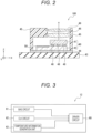
- Fig. 2 is a cross-sectional view illustrating a structural example of the distance measuring device 100 according to the first embodiment of the present disclosure.
- the distance measuring device 100 includes the LD chip 41 (an example of a "second substrate” of the present disclosure) and the LDD substrate 42 (an example of a "first substrate” of the present disclosure) described above, a mounting substrate 43, a heat dissipation substrate 44, a correction lens holder 45, one or more correction lenses 46 (an example of a "lens" of the present disclosure), and a plurality of bump electrodes 48.
- the LD chip 41 an example of a "second substrate” of the present disclosure
- the LDD substrate 42 an example of a "first substrate” of the present disclosure
- the X-axis direction and the Y-axis direction correspond to the horizontal direction
- the Z-axis direction corresponds to the vertical direction
- the arrow direction of the Z axis corresponds to the upward direction
- the opposite of the arrow direction corresponds to the downward direction.
- the LDD substrate 42 is disposed on the mounting substrate 43 via the heat dissipation substrate 44.
- an LD chip 41 is disposed on the LDD substrate 42.
- the LD chip 41 is flip chip-mounted on the LDD substrate 42.
- the mounting substrate 43 is, for example, a printed board.
- the mounting substrate 43 is provided with the image sensor 21 and the image processing unit 22 illustrated in Fig. 1 .
- the heat dissipation substrate 44 is, for example, a ceramic substrate such as an aluminum nitride (AlN) substrate.
- the correction lens holder 45 is disposed on the heat dissipation substrate 44 so as to surround the LD chip 41, and holds one or more correction lenses 46 above the LD chip 41. These correction lenses 46 are included in the light-emitting-side optical system 14 described above (cf. Fig. 1 ). The correction lenses 46 are disposed at a position facing the LDD substrate 42 across the LD chip 41. Light emitted from the light-emitting unit 11 (cf. Fig. 1 ) in the LD chip 41 is incident on and corrected by these correction lenses 46, and the subject is then irradiated with the light (cf. Fig. 1 ).
- Fig. 2 illustrates two correction lenses 46 held by correction lens holder 45 as an example of the first embodiment.
- the plurality of bump electrodes 48 is provided on at least one of the upper surface of the LDD substrate 42 or the lower surface of the LD chip 41 and electrically connects the LDD substrate 42 and the LD chip 41.
- the bump electrode 48 is made of an arbitrary metal material such as gold (Au), nickel (Ni), or aluminum (Al).
- the LDD substrate 42 is provided with a light-shielding film 50 (an example of a "light-shielding unit” of the present disclosure) that shields at least a part of the drive circuit 12 from light emitted by the light-emitting unit 11 provided in the LD chip 41.
- the light-shielding film 50 may be provided on the upper surface 42a of the LDD substrate 42 or may be provided inside the LDD substrate 42.
- a structural body in which the LD chip 41 including the VCSEL is flip chip-mounted on the LDD substrate 42 is referred to as a VCSEL mounted body 40.
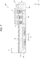
- Fig. 3 is a block diagram illustrating a configuration example of the drive circuit 12 according to the first embodiment of the present disclosure.
- the drive circuit 12 includes a driver circuit 60 that drives the light-emitting unit 11 (cf. Fig. 1 ), a bias circuit 61, a clock (CLK) circuit 62, and a temperature information generation unit 63.
- the bias circuit 61 generates a reference current from the power supply voltage supplied from the power supply circuit 13 and supplies the generated reference current to the driver circuit 60.
- the CLK circuit 62 generates a clock signal for controlling the light emission timing of the light-emitting unit 11 and supplies the generated clock signal to the driver circuit 60.
- the temperature information generation unit 63 measures the temperature of the LDD substrate 42, generates a signal including temperature information, and supplies the generated signal to the driver circuit 60. As illustrated in Fig. 2 , since the LD chip 41 is flip chip-mounted on the LDD substrate 42, the temperature of the LDD substrate 42 is correlated with the temperature of the LD chip 41.
- the driver circuit 60 controls the light emission timing of the light-emitting unit 11 on the basis of the supplied clock signal. In addition, the driver circuit 60 corrects a current value to be applied to the light-emitting unit 11 on the basis of the signal supplied from the temperature information generation unit 63. As a result, the driver circuit 60 can reduce the fluctuation of the intensity of the light emitted from the light-emitting unit 11 due to the temperature.
- Fig. 4 is a cross-sectional view illustrating a structural example of the VCSEL mounted body 40 according to the first embodiment of the present disclosure.
- the VCSEL mounted body 40 includes the LDD substrate 42, the LD chip 41, and the bump electrode 48 electrically connecting the LDD substrate 42 and the LD chip 41.
- the LDD substrate 42 has the upper surface 42a (an example of "one surface” of the present disclosure) and a lower surface 42b, and the LD chip 41 is flip chip-mounted on the upper surface 42a side via the bump electrode 48.
- the LDD substrate 42 has a substrate body 421 made of Si, for example.
- the upper surface 42a of the LDD substrate 42 is an upper surface of the substrate body 421, and a lower surface 42b of the LDD substrate 42 is a lower surface of the substrate body 421.
- the substrate body 421 includes the driver circuit 60, the bias circuit 61, the CLK circuit 62 (cf. Fig. 3 ), and the temperature information generation unit 63 (cf. Fig. 3 ).
- the driver circuit 60 and the bias circuit 61 are provided on the lower surface 42b side of the substrate body 421.
- the driver circuit 60 and the bias circuit 61 are electrically connected to each other via a wiring layer (or at least a part of wiring layers 71 to 73 to be described later) (not illustrated).
- the bias circuit 61 includes a well layer 611, an npn bipolar transistor 612 provided in the well layer 611, and a pnp bipolar transistor 613 provided in the well layer 611.
- the substrate body 421 is provided with the light-shielding film 50, a pad electrode 70, and a plurality of wiring layers 71 to 73.
- the light-shielding film 50 and the pad electrode 70 are provided on the upper surface 42a of the substrate body 421.
- the wiring layers 71 to 73 are provided inside the substrate body 421.
- the pad electrode 70 is located above the driver circuit 60, and the plurality of wiring layers 71 to 73 is provided between the driver circuit 60 and the pad electrode 70.
- the driver circuit 60 and the pad electrode 70 are electrically connected to each other via the plurality of wiring layers 71 to 73 and a through electrode (not illustrated) that connects the wiring layers 71 to 73 in the vertical direction (Z-axis direction).
- the light-shielding film 50 is made of a metal having a light-shielding property against infrared light, such as aluminum (Al) or copper (Cu).
- the light-shielding film 50 covers the entire region of the bias circuit 61 from the upper surface 42a side of the substrate body 421.
- the light-shielding film 50 may be provided on the same layer as the pad electrode 70 as illustrated in Fig. 4 or may be provided on a layer different from the pad electrode 70. In a case where the light-shielding film 50 is provided on the same layer as the pad electrode 70, the light-shielding film 50 and the pad electrode 70 may be simultaneously formed in the same process.
- the bump electrode 48 is provided on the pad electrode 70.
- the driver circuit 60 is electrically connected to the LD chip 41 via the plurality of wiring layers 71 to 73, the pad electrode 70, and the bump electrode 48.
- the correction lens 46 (cf. Fig. 2 ) is disposed above the LD chip 41.
- the distance measuring device 100 includes the LDD substrate 42 having the drive circuit 12, the LD chip 41 having the light-emitting unit 11 driven by the drive circuit 12, and the light-shielding film 50.
- the LD chip 41 is flip chip-mounted on the upper surface 42a side of the LDD substrate 42.
- the light-shielding film 50 is provided on the LDD substrate 42 and shields at least a part of the drive circuit 12 (e.g., bias circuit 61) from light (e.g., infrared light) emitted by the light-emitting unit 10.
- the light-shielding film 50 prevents the incidence of infrared light on the bias circuit 61.
- the light-shielding film 50 can reduce the occurrence of a photovoltaic effect on the p-n junction surface of the element, such as the bipolar transistors 612, 613, included in the bias circuit 61 and can reduce a change in characteristics of the element due to the photovoltaic effect. Thus, the light-shielding film 50 can reduce the possibility that the drive circuit 12 malfunctions.
- the bias circuit 61 has the highest sensitivity to light and the largest area. Therefore, in the first embodiment of the present disclosure, it is particularly preferable to shield the bias circuit 61 from light.
- the bias circuit 61 generates a reference current, but when the bias circuit 61 is irradiated with infrared light, the characteristics of the elements, such as the bipolar transistors 612, 613, change due to the photovoltaic effect, and the reference current fluctuates. When the fluctuation of the reference current is large, the drive circuit 12 is likely to malfunction. By shielding the bias circuit 61 from light, it is possible to reduce the fluctuation of the reference current and to reduce the possibility that the drive circuit 12 malfunctions.
- the light-shielding film 50 is disposed in the region overlapping with the bias circuit 61 in the thickness direction (e.g., in the Z-axis direction) of the LDD substrate 42, and the bias circuit 61 is not disposed in the other regions.
- the first embodiment of the present disclosure is not limited thereto.
- the light-shielding film 50 in the Z-axis direction, may be disposed in a region overlapping with the driver circuit 60 (cf. Fig. 3 ), the light-shielding film 50 may be disposed in a region overlapping with the CLK circuit 62 (cf. Fig.
- the light-shielding film 50 may be disposed in a region overlapping with the temperature information generation unit 63 (cf. Fig. 3 ). Hence the light-shielding film 50 can prevent the incidence of infrared light on the driver circuit 60, the CLK circuit 62, and the temperature information generation unit 63.
- any of the driver circuit 60, the CLK circuit 62, and the temperature information generation unit 63 includes an element including a p-n junction surface, such as a bipolar transistor or a MOS transistor, but the light-shielding film 50 can reduce the generation of the photovoltaic effect on the p-n junction surface by preventing the incidence of infrared light. As a result, the light-shielding film 50 can reduce a change in the characteristics of the element due to the photovoltaic effect in any of the driver circuit 60, the CLK circuit 62, and the temperature information generation unit 63 and can reduce the possibility that the drive circuit 12 malfunctions.
- the coverage by the light-shielding film 50 is preferably high.
- the coverage per unit area by the light-shielding film 50 is preferably 50% or more, more preferably 65% or more, and still more preferably 80% or more, except for a region where the LD chip 41 is mounted.
- the light-shielding film 50 may be provided to cover the entire upper surface 42a of the LDD substrate 42 except for the region where the LD chip 41 is mounted (i.e., so as to make the coverage 1000.).
- An example in which the coverage per unit area is 100% except for the region where the LD chip 41 is mounted is illustrated in Fig. 5 below.
- Fig. 5 is a cross-sectional view illustrating a configuration example of a VCSEL mounted body 40A according to Modification 1 of the first embodiment of the present disclosure.
- the light-shielding film 50 is provided to cover the entire upper surface 42a of the LDD substrate 42 except for the region where the LD chip 41 is mounted.
- the light-shielding film 50 can prevent the incidence of infrared light not only on the bias circuit 61 but also on the driver circuit 60, the CLK circuit 62, and the temperature information generation unit 63.
- the light-shielding film 50 can further reduce a change in the characteristics of each element provided on the LDD substrate 42 due to the photovoltaic effect and can further reduce the possibility that the drive circuit 12 malfunctions.
- some of the wiring layers 71 to 73 may function as a light-shielding unit.
- the wiring layer functioning as the light-shielding unit is made of a metal having a light-shielding property against infrared light, such as aluminum (Al) or copper (Cu).
- Fig. 6 is a cross-sectional view illustrating a configuration example of a VCSEL mounted body 40B according to Modification 2 of the first embodiment of the present disclosure.
- a part of the wiring layer 71 extends to above the bias circuit 61.
- the bias circuit 61 includes a first region R1 overlapping with the light-shielding film 50 in the thickness direction (e.g., in the Z-axis direction) of the LDD substrate 42 and a second region R2 not overlapping with the light-shielding film 50 in the Z-axis direction.
- the wiring layer 71 covers at least a part of the second region R2.
- the wiring layer 71 is made of a metal having a light-shielding property against infrared light, such as aluminum (Al) or copper (Cu).
- the positions of the light-shielding film 50 and the wiring layer 71 in the horizontal direction are shifted from each other.
- the light-shielding film 50 and the wiring layer 71 in such a positional relationship prevent the incidence of infrared light on the bias circuit 61. Therefore, similarly to the first embodiment described above, it is possible to reduce a change in characteristics of the element due to the photovoltaic effect, and it is possible to reduce the possibility that the drive circuit 12 malfunctions.
- the bias circuit 61 is preferably disposed at a position away from a side surface 42c of the outer periphery of the LDD substrate 42.
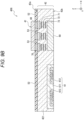
- Fig. 7 is a cross-sectional view illustrating a configuration example of a VCSEL mounted body 40C according to Modification 3 of the first embodiment of the present disclosure. As illustrated in Fig. 7 , in the VCSEL mounted body 40C according to Modification 3, the bias circuit 61 is disposed at a position sufficiently away from the side surface 42c of the outer periphery of the LDD substrate 42. For example, a distance d from the side surface 42c of the outer periphery of the LDD substrate to the bias circuit 61 is 500 ⁇ m or more.
- the bias circuit 61 is disposed at a position sufficiently away from the side surface 42c of the outer periphery of the LDD substrate 42, so that it is possible to reduce the possibility that the light incident from the side surface 42c reaches the bias circuit 61. It is thereby possible to further reduce a change in the characteristics of the bias circuit 61 due to the photovoltaic effect.
- a through layer made of a light-shielding material may be provided between the side surface 42c of the outer periphery of the LDD substrate 42 and the drive circuit 12 (cf. Fig. 1 ).
- Fig. 8A is a cross-sectional view illustrating a configuration example of a VCSEL mounted body 40D according to Modification 4A of the first embodiment of the present disclosure.
- the LDD substrate 42 has a through layer 51 penetrating the LDD substrate 42 in the thickness direction (e.g., in the Z-axis direction) of the LDD substrate 42.
- the through layer 51 is made of a metal having a light-shielding property against infrared light, such as aluminum (Al) or copper (Cu).
- the through layer 51 is provided between the side surface 42c of the outer periphery of the LDD substrate 42 and the bias circuit 61 and is provided in a ring shape along the side surface 42c of the outer periphery, for example.
- the bias circuit 61 is shielded by the through layer 51 provided along the side surface 42c of the outer periphery, so that it is possible to reduce the possibility that the light incident from the side surface 42c reaches the bias circuit 61 It is thereby possible to further reduce a change in the characteristics of the bias circuit 61 due to the photovoltaic effect.
- Fig. 8B is a cross-sectional view illustrating a configuration example of a VCSEL mounted body 40E according to Modification 4B of the first embodiment of the present disclosure.
- a plurality of through layers 51 may be provided instead of one through layer.
- two through layers 51, or three or more through layers 51 may be provided along the side surface 42c of the outer periphery. With such a configuration, it is possible to further reduce the possibility that the light incident from the side surface 42c reaches the bias circuit 61.
- the light-shielding film 50 is made of a metal such as aluminum (Al) or copper (Cu).
- the first embodiment of the present disclosure is not limited thereto.
- the light-shielding film 50 may be made of, for example, resin.
- Fig. 9A is a cross-sectional view illustrating a configuration example of a VCSEL mounted body 40F according to Modification 5A of the first embodiment of the present disclosure.
- the VCSEL mounted body 40F according to Modification 5A includes a light-shielding film 52 instead of the light-shielding film 50 made of metal.
- the light-shielding film 52 is made of a resin having a light-shielding property against infrared light. Even with such a configuration, the light-shielding film 52 can prevent the incidence of infrared light on the bias circuit 61 and can reduce a change in characteristics of the element due to the photovoltaic effect. Hence the light-shielding film 52 can reduce the possibility that the drive circuit 12 malfunctions.
- a gap between the LDD substrate 42 and the LD chip 41 may be filled with an insulating resin 53.
- the resin 53 may be referred to as an underfill material.
- the resin 53 can enhance reliability of the connection between the LDD substrate 42 and the LD chip 41.
- an epoxy resin can be used as the resin 53.
- the resin 53 and the light-shielding film 52 described above may have the same composition.
- the resin 53 and the light-shielding film 52 described above may be formed simultaneously in the same step. Accordingly, there is a possibility that the number of steps can be reduced at the time of manufacturing the VCSEL mounted body 40F, and there is a possibility that the manufacturing cost can be reduced.
- Fig. 9B is a cross-sectional view illustrating a configuration example of a VCSEL mounted body 40G according to Modification 5B of the first embodiment of the present disclosure.
- the light-shielding film 52 may be provided on the entire upper surface 42a of the LDD substrate 42 except for the region where the LD chip 41 is mounted. With such a configuration, the light-shielding film 52 can prevent the incidence of infrared light not only on the bias circuit 61 but also on the CLK circuit 62 and the temperature information generation unit 63, so that it is possible to further reduce the possibility that the drive circuit 12 malfunctions.
- the LDD substrate 42 may have a wire bonding pad electrode (WB pad electrode) to which a wire such as a gold wire is connected.
- WB pad electrode wire bonding pad electrode
- An opening that exposes the surface of the WB pad electrode is provided on the WB pad electrode, and a wire is connected to the surface of the WB pad electrode through the opening.
- the light-shielding film 50 may cover not only the upper portion of the drive circuit 12 but also the periphery of the wire bonding pad electrode.
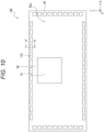
- Fig. 10 is a plan view illustrating a structural example of a VCSEL mounted body 140 according to a second embodiment of the present disclosure.
- a VCSEL mounted body 140 according to the second embodiment is a structural body in which a laser diode (LD) chip 41 including a VCSEL is flip chip-mounted on an LDD substrate 42, similarly to the VCSEL mounted body 40 illustrated in Fig. 4 .
- the VCSEL mounted body 140 is disposed on the mounting substrate 43 via the heat dissipation substrate 44 instead of the VCSEL mounted body 40.
- the LDD substrate 42 has a plurality of WB pad electrodes 110 (an example of a "wire bonding pad electrode" of the present disclosure) provided on the upper surface 42a side of the LDD substrate 42, and a protective film 120 provided on the upper surface 42a side of the LDD substrate 42.
- the WB pad electrode 110 is a pad electrode for connecting a wire such as a gold wire (not illustrated).
- the plurality of WB pad electrodes 110 is provided on the outer peripheral portion of the LDD substrate 42 in a plan view from the normal direction (e.g., Z-axis direction) of the upper surface 42a of the LDD substrate 42 and is arranged at regular intervals so as to draw a rectangular frame along the outer periphery of the LDD substrate 42.
- Fig. 11 is an enlarged plan view illustrating the WB pad electrode 110 and its peripheral portion illustrated in Fig. 10 .
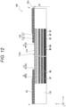
- Fig. 12 is a cross-sectional view illustrating a configuration example of the VCSEL mounted body 40 according to the second embodiment of the present disclosure.
- Fig. 12 illustrates the cross-section of the plan view illustrated in Figs. 10 and 11 taken along line A-A'. Note that the cross-section of the plan view illustrated in Fig. 11 taken along line B-B' has a similar configuration to the cross-section of the plan view illustrated in Fig. 11 taken along line A-A'.
- the protective film 120 includes an opening H120 that exposes the surface of the WB pad electrode 110.
- the opening H120 is located inside the WB pad electrode 110, and the bottom surface of the opening H120 is the surface of the WB pad electrode 110.
- the light-shielding film 50 is provided on the protective film 120.
- the light-shielding film 50 is also provided with an opening H50.
- the opening H50 provided in the light-shielding film 50 is located above the WB pad electrode 110 and communicates with the opening H120 provided in the protective film 120.
- the WB pad electrode 110 is made of, for example, aluminum (Al) or an Al alloy containing Al.
- the protective film 120 includes, for example, a silicon oxide film (SiO 2 film) 121 and a silicon nitride film (SiN) 122 provided on the SiO 2 film 121.
- the light-shielding film 50 includes, for example, titanium (Ti) and gold (Au) provided on Ti.
- a plurality of (e.g., seven) wires M1 to M7 stacked in the Z-axis direction via the interlayer insulating film 130 is provided below the WB pad electrode 110.
- the wires M6, M7 are power supply lines.
- the wires M1 to M5 are signal lines. At least some of the wires M1 to M7 located below the WB pad electrode 110 may be dummy wires that are not electrically connected to an element such as a transistor.
- the light-shielding film 50 can reduce the entry of light into the LDD substrate 42 from the periphery of the WB pad electrode 110 and can further reduce the possibility that the drive circuit 12 malfunctions.
- a portion of the light-shielding film 50 disposed around the WB pad electrode 110 is an example of a "peripheral light-shielding unit" of the present disclosure.
- the opening H120 for exposing the surface of the WB pad electrode 110 is provided on the WB pad electrode 110, and a wire is connected to the surface of the WB pad electrode 110 through the opening H120.
- the side surface of the opening H120 being exposed from the light-shielding film 50, there is a possibility that the side surface becomes an entrance of light into the LDD substrate 42.
- the side surface of the opening H120 may be covered with a peripheral light-shielding unit. As such an aspect, Configuration Examples 1 to 3 of the third embodiment will be described.
- Fig. 13 is a cross-sectional view illustrating a configuration example (Configuration Example 1) of a VCSEL mounted body 140A according to a third embodiment of the present disclosure.
- a light-shielding resin 210 is applied around the opening H120.
- the light-shielding resin 210 is an insulating resin.
- the light-shielding resin 210 has a light-shielding property against light emitted from the light-emitting unit 11.
- the light-shielding resin 210 is a dark or black insulating resin and has a shielding property against infrared light emitted from the light-emitting unit 11.
- the light-shielding resin 210 may be a resin called a black matrix.
- the light-shielding resin 210 continuously covers the light-shielding film 50, a side surface s2 of the opening H50 provided in the light-shielding film 50, the top of the protective film 120 exposed from below the light-shielding film 50, a side surface s1 of the opening H120 provided in the protective film 120, and the top of the WB pad electrode 110 located in the vicinity of the side surface s1 of the opening H120.
- An interface end between the WB pad electrode 110 and the protective film 120 and the side surface s1 of the opening H120 can be cited as an entrance of light (ambient light) from the opening H120 to the LDD substrate 42.
- an interface end between the protective film 120 and the light-shielding film 50 can be cited as an entrance of the ambient light from the opening H50 into the LDD substrate 42.
- the light-shielding resin 210 covers and closes these entrances.
- the light-shielding resin 210 covers the side surfaces s1, s2 of the openings H120, H50.
- the light-shielding resin 210 can prevent ambient light from entering the LDD substrate 42 through the openings H120, H50 and can shield at least some (e.g., the bias circuit 61) of the drive circuit 12 from the ambient light. Therefore, the light-shielding resin 210 can further reduce the possibility that the drive circuit 12 malfunctions.
- the light-shielding resin 210 preferably covers the entire side surface s1 of the opening H120. Hence the light-shielding resin 210 easily shields the entrance of the ambient light present on the side surface s1 of the opening H120 and the like.
- the light-shielding resin 210 may be disposed to cover not the entire side surface s1 of the opening H120 but a part of the side surface s1.
- the light-shielding resin 210 may be applied so as to cover the side surface on the side closer to the drive circuit 12 and so as not to cover the side surface on the side farther from the drive circuit 12 among the side surfaces s1 of the opening H120.
- there is a possibility that the entry of the ambient light into the drive circuit 12 can be reduced as compared with a case where the side surface on the side close to the drive circuit 12 is not covered with the light-shielding resin 210.
- Fig. 14 is a cross-sectional view illustrating a configuration example (Configuration Example 2) of a VCSEL mounted body 140B according to the third embodiment of the present disclosure.
- the WB pad electrode 110 has a thick film portion 111 (an example of the "peripheral light-shielding unit" of the present disclosure) having an increased thickness inside the opening H120.
- the WB pad electrode 110 includes a thick film portion 111 located inside the opening H120 and the other portion 112 located outside the opening H120.
- the thick film portion 111 and the other portion 112 are made of the same material and are integrally formed.
- the thick film portion 111 of the WB pad electrode 110 covers and closes the side surface s1 of the opening H120 serving as the entrance of the ambient light and the interface end between the WB pad electrode 110 and the protective film 120.
- the thick film portion 111 of the WB pad electrode 110 can prevent ambient light from entering the LDD substrate 42 through the opening H120 and can shield at least a part (e.g., the bias circuit 61) of the drive circuit 12 from the ambient light. Therefore, the thick film portion 111 can further reduce the possibility that the drive circuit 12 malfunctions.
- the thick film portion 111 preferably covers the entire side surface s1 of the opening H120. Hence the thick film portion 111 easily shields the entrance of the ambient light existing on the side surface s1 of the opening H120 and the like.
- the thick film portion 111 may be disposed to cover not the entire side surface s1 of the opening H120 but a part of the side surface s1.
- the thick film portion 111 may be formed so as to cover the side surface on the side closer to the drive circuit 12 and so as not to cover the side surface on the side farther from the drive circuit 12 among the side surfaces s1 of the opening H120. In this case, there is a possibility that the entry of the ambient light into the drive circuit 12 can be reduced as compared with a case where the side surface on the side close to the drive circuit 12 is not covered with the thick film portion 111.
- FIG. 15 is a cross-sectional view illustrating a configuration example (Configuration Example 3) of a VCSEL mounted body 140C according to the third embodiment of the present disclosure.
- a VCSEL mounted body 140C illustrated in Fig. 15 includes a sidewall 211 disposed on the side surface s1 of the opening H120 provided in the protective film 120, and a sidewall 212 disposed on the side surface s2 of the opening H50 provided in the light-shielding film 50.
- Each of the sidewalls 211, 212 is an example of the "peripheral light-shielding unit" of the present disclosure.
- the sidewalls 211, 212 are made of an insulating resin.
- the sidewalls 211, 212 have a light-shielding property against light emitted from the light-emitting unit 11.
- the sidewalls 211, 212 are made of a dark or black resin and have a shielding property against infrared light emitted from the light-emitting unit 11.
- the resin constituting the sidewalls 211, 212 may be made of a resin called a black matrix.
- the sidewalls 211, 212 are formed, for example, by applying an insulating dark or black resin to the upper surface 42a of the LDD substrate 42 in which the openings H120, H50 are formed, and etching back the applied resin.
- the sidewall 211 covers and closes the side surface s1 of the opening H120 serving as an entrance for the ambient light, and the interface end between the WB pad electrode 110 and the protective film 120.
- the sidewall 212 covers and closes the interface end between the protective film 120 and the light-shielding film 50 serving as the entrance of the ambient light.
- the sidewalls 211, 212 can prevent the entry of ambient light from the openings H120, H50 into the LDD substrate 42 and can shield at least a part (e.g., the bias circuit 61) of the drive circuit 12 from the ambient light. Therefore, the sidewalls 211, 212 can further reduce the possibility that the drive circuit 12 malfunctions.
- the sidewall 211 preferably covers the entire side surface s1 of the opening H120. Hence the sidewall 211 easily shields the entrance of the ambient light existing on the side surface s1 of the opening H120 and the like.
- the sidewall 212 preferably covers the entire side surface s2 of the opening H50. Hence the sidewall 211 easily shields the entrance of the ambient light existing in the vicinity of the side surface s2 of the opening H50.
- Configuration Example 3 of the third embodiment is not limited to the above.
- only one of the sidewalls 211, 212 may be provided.
- the sidewall 211 may be disposed to cover not the entire side surface s1 of the opening H120 but a part of the side surface s1.
- the sidewall 211 may be formed so as to cover the side surface on the side closer to the drive circuit 12 and so as not to cover the side surface on the side farther from the drive circuit 12 among the side surfaces s1 of the opening H120. In this case, there is a possibility that the entry of the ambient light into the drive circuit 12 can be reduced as compared with a case where the side surface on the side close to the drive circuit 12 is not covered with the sidewall 211.
- the sidewall 212 may be disposed to cover not the entire side surface s2 of the opening H50 but a part of the side surface s2.
- the sidewall 212 may be formed so as to cover the side surface on the side closer to the drive circuit 12 and so as not to cover the side surface on the side farther from the drive circuit 12 among the side surfaces s2 of the opening H50.
- the peripheral light-shielding unit may be disposed to shield the propagation path of the ambient light having entered from the opening H120 or the like.
- Configuration Examples 1 to 4 of the fourth embodiment will be described.
- Fig. 16 is a cross-sectional view illustrating a configuration example (Configuration Example 1) of a VCSEL mounted body 140D according to a fourth embodiment of the present disclosure.
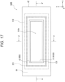
- Fig. 17 is an enlarged plan view illustrating the WB pad electrode 110 and its peripheral portion illustrated in Fig. 16 .
- the cross-section illustrated in Fig. 16 is a cross-section obtained by cutting the plan view illustrated in Fig. 17 along line A-A'. Note that the cross-section of the plan view illustrated in Fig. 17 taken along line B-B' has a similar configuration to the cross-section of the plan view illustrated in Fig. 17 taken along line A-A'.
- an opaque member 221 (an example of the "peripheral light-shielding unit" of the present disclosure) is disposed between the WB pad electrode 110 and the protective film 120 and blocks the propagation path of the ambient light.
- the opaque member 221 absorbs and attenuates the ambient light propagating along the propagation path.
- the opaque member 221 is made of, for example, titanium nitride (TiN).
- TiN is formed by forming a film by a semiconductor manufacturing process, such as chemical vapor deposition (CVD) or sputtering, and using a photolithography technique to perform patterning.
- the opaque member 221 is preferably in contact with the SiN film 122.
- the opaque member 221 can divide the SiO 2 film 121 on the WB pad electrode 110 and can absorb and attenuate ambient light propagating in the SiO 2 film 121.
- the SiO 2 film 121 is formed on the LDD substrate 42, the surface of the SiO 2 film 121 is subjected to chemical mechanical polishing (CMP) treatment to expose the surface of the opaque member 221, and then the SiN film 122 is formed, whereby the opaque member 221 can be brought into contact with the SiN film 122.
- CMP chemical mechanical polishing
- the opaque member 221 shields the propagation path of the ambient light, so that at least a part (e.g., the bias circuit 61) of the drive circuit 12 can be shielded from the ambient light. Therefore, the opaque member 221 can further reduce the possibility that the drive circuit 12 malfunctions.
- the opaque member 221 is preferably provided continuously so as to surround the opening H120 from the outside in a plan view from the Z-axis direction. Hence the opaque member 221 can easily shield the propagation path of the ambient light.
- Configuration Example 1 of the fourth embodiment is not limited to the above.
- the opaque member 221 may be intermittently provided to surround the opening H120 from the outside in cross-sectional view from the axial direction.
- the opaque member 221 may not necessarily surround the opening H120.
- Fig. 18 is a plan view illustrating a modification of the placement of the opaque member 221.
- the opaque member 221 may be disposed inside and outside a rectangular frame formed by a plurality of WB pad electrodes 110 arranged in a plan view from the Z-axis direction. Even with such a configuration, the opaque member 221 can shield the propagation path of the ambient light.
- the opaque member 221 may be disposed only on one of the inside or the outside of the rectangular frame formed by the plurality of WB pad electrodes 110 arranged in the plan view from the Z-axis direction.
- the opaque member 221 may be disposed only inside the rectangular frame, which is the side closer to the drive circuit 12. In this case, there is a possibility that the propagation of the ambient light to the drive circuit 12 can be reduced as compared with a case where the opaque member 221 is disposed only outside the rectangular frame.
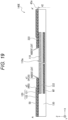
- Fig. 19 is a cross-sectional view illustrating a configuration example (Configuration Example 2) of a VCSEL mounted body 140E according to the fourth embodiment of the present disclosure.
- an antireflection film 222 (an example of the "peripheral light-shielding unit" of the present disclosure) is provided between the WB pad electrodes 110 and the protective film 120 and blocks the propagation path of the ambient light.
- the antireflection film 222 absorbs and attenuates ambient light propagating while being reflected between the WB pad electrode 110 and the SiN film 122 and reduces the propagation of the ambient light.
- the antireflection film 222 is made of, for example, a photoresist.
- the antireflection film 222 is formed by forming a film by a semiconductor manufacturing process, such as CVD or sputtering, and using a photolithography technique to perform patterning.
- the antireflection film 222 shields the propagation path of the ambient light, so that at least a part (e.g., the bias circuit 61) of the drive circuit 12 can be shielded from the ambient light. Therefore, the antireflection film 222 can further reduce the possibility that the drive circuit 12 malfunctions.
- the antireflection film 222 is preferably provided continuously to surround the opening H120 from the outside in a plan view from the Z-axis direction as in the opaque member 221 illustrated in Fig. 17 . Hence the antireflection film 222 can easily shield the propagation path of the ambient light.
- Configuration Example 1 of the fourth embodiment is not limited to the above.
- the antireflection film 222 may be intermittently provided to surround the opening H120 from the outside in cross-sectional view from the axial direction. In addition, the antireflection film 222 may not necessarily surround the opening H120.
- the modification illustrated in Fig. 18 may also be applied to Configuration Example 2 of the fourth embodiment.
- the opaque member 221 may be replaced with the antireflection film 222.
- the antireflection film 222 may be disposed on at least one of the inside or the outside of the rectangular frame formed by the plurality of WB pad electrodes 110 arranged in the plan view from the Z-axis direction. Even in this case, the antireflection film 222 can shield the propagation path of the ambient light.
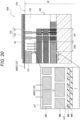
- Fig. 20 is a cross-sectional view illustrating a configuration example (Configuration Example 3) of a VCSEL mounted body 140F according to the fourth embodiment of the present disclosure.
- the right end of the right diagram in Fig. 20 is the outer peripheral end of the LDD substrate 42.
- the diagram on the left side of Fig. 20 is an enlarged cross-sectional view illustrating a light-shielding dummy wiring layer DML (an example of the "peripheral light-shielding unit" of the present disclosure) provided on the LDD substrate 42.
- DML an example of the "peripheral light-shielding unit" of the present disclosure
- a guard ring GR exists between the WB pad electrode 110 and the outer peripheral end 42E of the LDD substrate 42 in order to prevent the entry of moisture, impurities, and the like.
- the guard ring GR is formed of a metal layer formed in the same layer as the wires M1 to M7 and the WB pad electrode 110.
- the metal layer constituting the guard ring GR is a dummy wire or a dummy electrode that is not electrically connected to an element such as a transistor.
- the light-shielding dummy wiring layer DML is disposed on the outer periphery of the WB pad electrode 110 and a region immediately below the WB pad electrode.
- the dummy wiring layer DML is disposed between the WB pad electrode / the region immediately below the WB pad electrode 110 and the guard ring GR.
- the dummy wiring layer DML may be disposed on the entire outer periphery of the WB pad electrode 110 and the region immediately below the WB pad electrode or may be disposed on a part of the outer periphery of the WB pad electrode 110.
- a plurality of dummy wires is arranged to overlap with each other in order to shield ambient light.
- a dummy wire DM7 and a dummy wire DM6 are metal wiring layers formed in the same layer as the power supply wires M7, M6 (cf. Fig. 12 ).
- Dummy wires DM5, DM4 are metal wiring layers formed in the same layer as the signal wires M5, M4 (cf. Fig. 12 ).
- the dummy wires DM7, DM6, DM5, DM4 are not electrically connected to elements such as transistors.
- the dummy wire DM7 (an example of a "(n + m)th layer dummy wire” of the present disclosure) and the dummy wire DM6 (an example of an "nth layer dummy wire” of the present disclosure) overlap with each other such that the dummy wire DM6 overlaps with an inter-wire space sp7 of the dummy wire DM7.
- the ambient light is transmitted through the inter-wire space sp7 of the dummy wire DM7
- the light transmitted through the inter-wire space sp7 is reflected by the dummy wire DM6 located ahead of the inter-wire space sp7 and is attenuated.
- the dummy wire DM5 (an example of the "(n + m)th layer dummy wire” of the present disclosure) and the dummy wire DM4 (an example of the "nth layer dummy wire” of the present disclosure) overlap with each other such that the dummy wire DM4 overlaps with an inter-wire space sp5 of the dummy wire DM5.
- the ambient light is transmitted through the inter-wire space sp5 of the dummy wire DM5
- the light transmitted through the inter-wire space sp5 is reflected by the dummy wire DM4 located ahead of the inter-wire space sp5 and is attenuated.
- the dummy wiring layer DML can shield the propagation path of the ambient light.
- the dummy wiring layer DML can reduce the propagation of the ambient light and can shield at least a part (e.g., the bias circuit 61) of the drive circuit 12 from the ambient light. Therefore, the dummy wiring layer DML can further reduce the possibility that the drive circuit 12 malfunctions.
- the dummy wires to be overlapped are preferably adjacent wires in the thickness direction of the LDD substrate 42, such as the dummy wire DM7 and the dummy wire DM6 or the dummy wire DM5 and the dummy wire DM4. That is, m in the n + m layer described above is preferably 1. Hence it is possible to reduce the diffraction of the ambient light transmitted through the inter-wire space to a small degree, and it is possible to more effectively reduce the propagation of the ambient light.
- the modification illustrated in Fig. 18 may also be applied to Configuration Example 3 of the fourth embodiment.
- the opaque member 221 may be replaced with a dummy wiring layer DML.
- the dummy wiring layer DML may be disposed on at least one of the inside or the outside of the rectangular frame formed by the plurality of WB pad electrodes 110 arranged in the plan view from the Z-axis direction. Even in this case, the dummy wiring layer DML can shield the propagation path of the ambient light.
- Fig. 21 is a cross-sectional view illustrating a configuration example (Configuration Example 4) of a VCSEL mounted body 140G according to the fourth embodiment of the present disclosure.
- a light-shielding trench isolation 230 is disposed on the outer periphery of the WB pad electrode 110 and a region immediately below the WB pad electrode.
- the trench isolation 230 includes a trench 231 provided in the interlayer insulating film 130 and an embedded material 232 provided in the trench 231.
- the embedded material 232 is made of a material capable of absorbing or reflecting ambient light, such as polysilicon, metal, or a low-dielectric constant material (low-K material).
- the trench isolation 230 can shield the propagation path of the ambient light and reduce the propagation of the ambient light.
- the trench isolation 230 can shield at least a part (e.g., the bias circuit 61) of the drive circuit 12 from ambient light, so that it is possible to further reduce the possibility that the drive circuit 12 malfunctions.
- the light emitted by the light-emitting unit 11 is not limited to infrared light.
- the light emitted from the light-emitting unit 11 may be visible light or ultraviolet light.
- the light-shielding unit of the present disclosure may include both the light-shielding film 50 and the through layer 51.
- the present technology includes various embodiments and the like not described herein. At least one of various omissions, substitutions, or changes of the components can be made without departing from the gist of the embodiments and modifications described above.
- the effects described in the present specification are merely examples, are not limited, and may have other effects.
Landscapes
- Physics & Mathematics (AREA)
- Condensed Matter Physics & Semiconductors (AREA)
- General Physics & Mathematics (AREA)
- Electromagnetism (AREA)
- Optics & Photonics (AREA)
- Semiconductor Lasers (AREA)
Abstract
Description
- The present disclosure relates to an electronic device.
- As a type of semiconductor laser, a surface-emitting laser such as a vertical-cavity surface-emitting laser (VCSEL) is known (e.g., see
Patent Documents -
- Patent Document 1:
Japanese Unexamined Patent Application Publication (Translation of PCT Application) No. 2004-526194 - Patent Document 2:
Japanese Patent Application Laid-Open No. 2020-20680 -
Fig. 7A ofPatent Document 2 discloses a configuration in which a chip having a circuit as a light-emitting unit formed therein is flip chip-mounted on a chip in which a circuit as a drive unit is formed. In the device having this configuration, there is a possibility that a part of the light emitted from the light-emitting unit is reflected by the surface of the lens and incident on the drive unit. The drive unit has elements (e.g., bipolar transistors) each including a p-n junction surface. When light strikes these elements, a photovoltaic effect occurs, the characteristics of the elements change, and there is a possibility that the drive unit malfunctions. - The present disclosure has been made in view of such circumstances, and an object of the present disclosure is to provide an electronic device capable of reducing the possibility of malfunction.
- An electronic device according to one aspect of the present disclosure is provided with: a first substrate including a drive circuit; a second substrate including a light-emitting unit driven by the drive circuit and mounted on one surface side of the first substrate; and a light-shielding unit provided on the first substrate and configured to shield at least a part of the drive circuit from light emitted by the light-emitting unit.
- Accordingly, even in a case where a part of the light (e.g., infrared light) emitted from the light-emitting unit is reflected by the surface of the lens and directed to a part of the drive circuit (e.g., a bias circuit), this infrared ray is shielded by the light-shielding unit. The light-shielding unit can reduce the occurrence of a photovoltaic effect on a p-n junction surface of an element (e.g., bipolar transistor, etc.) included in the bias circuit and can reduce a change in characteristics of the element due to the photovoltaic effect. Thus, the light-shielding unit can reduce the possibility that the drive circuit malfunctions.
- An electronic device according to another aspect of the present disclosure is provided with: a first substrate including a drive circuit; a second substrate including a light-emitting unit driven by the drive circuit and mounted on one surface side of the first substrate; and a peripheral light-shielding unit having a light-shielding property against light emitted by the light-emitting unit. The first substrate includes a wire bonding pad electrode provided on one surface side of the first substrate, and a protective film provided on one surface side of the first substrate and provided with an opening that exposes the surface of the wire bonding pad electrode. The peripheral light-shielding unit is disposed around the wire bonding pad electrode.
- Accordingly, even in a case where a part of light (e.g., infrared light) emitted from the light-emitting unit is reflected by the surface of the lens and directed to the periphery of the wire bonding electrode, this infrared ray is shielded by the peripheral light-shielding unit. As a result, the peripheral light-shielding unit can reduce the entry of light into the first substrate from the periphery of the wire bonding electrode. Thus, the peripheral light-shielding unit can reduce the possibility that the drive circuit malfunctions.
-
-
Fig. 1 is a block diagram illustrating a configuration example of a distance measuring device according to a first embodiment of the present disclosure. -
Fig. 2 is a cross-sectional view illustrating a structural example of the distance measuring device according to the first embodiment of the present disclosure. -
Fig. 3 is a block diagram illustrating a configuration example of a drive circuit according to the first embodiment of the present disclosure. -
Fig. 4 is a cross-sectional view illustrating a structural example of a VCSEL mounted body according to the first embodiment of the present disclosure. -
Fig. 5 is a cross-sectional view illustrating a configuration example of a VCSEL mounted body according toModification 1 of the first embodiment of the present disclosure. -
Fig. 6 is a cross-sectional view illustrating a configuration example of a VCSEL mounted body according toModification 2 of the first embodiment of the present disclosure. -
Fig. 7 is a cross-sectional view illustrating a configuration example of a VCSEL mounted body according toModification 3 of the first embodiment of the present disclosure. -
Fig. 8A is a cross-sectional view illustrating a configuration example of a VCSEL mounted body according to Modification 4A of the first embodiment of the present disclosure. -
Fig. 8B is a cross-sectional view illustrating a configuration example of a VCSEL mounted body according to Modification 4B of the first embodiment of the present disclosure. -
Fig. 9A is a cross-sectional view illustrating a configuration example of a VCSEL mounted body according to Modification 5A of the first embodiment of the present disclosure. -
Fig. 9B is a cross-sectional view illustrating a configuration example of a VCSEL mounted body according to Modification 5B of the first embodiment of the present disclosure. -
Fig. 10 is a plan view illustrating a structural example of a VCSEL mounted body according to a second embodiment of the present disclosure. -
Fig. 11 is an enlarged plan view illustrating a wire bonding (WB) pad electrode and its peripheral portion illustrated inFig. 10 . -
Fig. 12 is a cross-sectional view illustrating a configuration example of a VCSEL mounted body according to the second embodiment of the present disclosure. -
Fig. 13 is a cross-sectional view illustrating Configuration Example 1 of the VCSEL mounted body according to a third embodiment of the present disclosure. -
Fig. 14 is a cross-sectional view illustrating Configuration Example 2 of the VCSEL mounted body according to the third embodiment of the present disclosure. -
Fig. 15 is a cross-sectional view illustrating Configuration Example 3 of the VCSEL mounted body according to the third embodiment of the present disclosure. -
Fig. 16 is a cross-sectional view illustrating Configuration Example 1 of the VCSEL mounted body according to a fourth embodiment of the present disclosure. -
Fig. 17 is an enlarged plan view illustrating a WB pad electrode and its peripheral portion illustrated inFig. 16 . -
Fig. 18 is a plan view illustrating a modification of the placement of an opaque member. -
Fig. 19 is a cross-sectional view illustrating Configuration Example 2 of the VCSEL mounted body according to the fourth embodiment of the present disclosure. -
Fig. 20 is a cross-sectional view illustrating Configuration Example 3 of the VCSEL mounted body according to the fourth embodiment of the present disclosure. -
Fig. 21 is a cross-sectional view illustrating Configuration Example 4 of the VCSEL mounted body according to the fourth embodiment of the present disclosure. - Hereinafter, a first embodiment of the present disclosure will be described with reference to the drawings. In the description of the drawings referred to in the following description, the same or similar parts are denoted by the same or similar reference numerals. However, it should be noted that the drawings are schematic, and the relationship between the thickness and the plane dimension, the ratio of the thickness of each layer, and the like are different from actual ones. Therefore, specific thicknesses and dimensions should be determined in consideration of the following description. In addition, it is needless to say that portions having different dimensional relationships and ratios are included between the drawings.
- The definition of directions, such as upper and lower, in the following description is merely a definition for convenience of description and does not limit the technical idea of the present disclosure. For example, it is a matter of course that when an object is rotated by 90 ° and observed, the upper and lower sides are converted to the left and right and read, and when the object is rotated by 180 ° and observed, the upper and lower parts are inverted and read.
- In the following description, there are cases where the direction is described using words in the X-axis direction, the Y-axis direction, and the Z-axis direction. For example, the X-axis direction and the Y-axis direction are directions parallel to an
upper surface 42a of a laser diode driver (LDD)substrate 42. The X-axis direction and the Y-axis direction are also referred to as horizontal directions. The Z-axis direction is a direction vertical to theupper surface 42a. The X-axis direction, the Y-axis direction, and the Z-axis direction are orthogonal to each other. -
Fig. 1 is a block diagram illustrating a configuration example of adistance measuring device 100 according to a first embodiment of the present disclosure. As illustrated inFig. 1 , thedistance measuring device 100 according to a first embodiment of the present disclosure (an example of an "electronic device" of the present disclosure) includes a light-emittingdevice 1, animaging device 2, and acontrol device 3. Thedistance measuring device 100 irradiates a subject with light emitted from the light-emittingdevice 1, receives the light reflected by the subject by theimaging device 2 to image the subject, and measures (calculates) a distance to the subject by thecontrol device 3 using an image signal output from theimaging device 2. The light-emittingdevice 1 functions as a light source for theimaging device 2 to image the subject. - The light-emitting
device 1 includes a light-emittingunit 11, adrive circuit 12, apower supply circuit 13, and a light-emitting-sideoptical system 14. Theimaging device 2 includes animage sensor 21, animage processing unit 22, and an imaging-sideoptical system 23. Thecontrol device 3 includes adistance measuring unit 31. - The light-emitting
unit 11 emits laser light for irradiating the subject. The light-emittingunit 11 includes a VCSEL. For example, the light-emittingunit 11 includes a plurality of light-emitting elements arranged in a two-dimensional array, and each light-emitting element has a VCSEL structure. The subject is irradiated with light emitted from these light-emitting elements. The light emitted from the light-emitting element is, for example, infrared light. The light-emittingunit 11 is provided in a chip called a laser diode (LD)chip 41. - The
drive circuit 12 is an electric circuit that drives the light-emittingunit 11. Thepower supply circuit 13 is an electric circuit that generates the power supply voltage of thedrive circuit 12. For example, thedistance measuring device 100 generates a power supply voltage from an input voltage supplied from a battery (not illustrated) by thepower supply circuit 13, supplies the generated power supply voltage to thedrive circuit 12, and drives the light-emittingunit 11 by thedrive circuit 12. The battery may be provided inside thedistance measuring device 100 or may be provided outside thedistance measuring device 100. Further, thedrive circuit 12 is provided in a substrate called a laser diode driver (LDD)substrate 42. - The light-emitting-side
optical system 14 includes various optical elements and irradiates the subject with light from the light-emittingunit 11 via these optical elements. Similarly, the imaging-sideoptical system 23 includes various optical elements and receives light from the subject via these optical elements. - The
image sensor 21 receives light from the subject via the imaging-sideoptical system 23 and converts the light into an electric signal by photoelectric conversion. Theimage sensor 21 is, for example, a charge-coupled device (CCD) sensor or a complementary metal-oxide-semiconductor (CMOS) sensor. Theimage sensor 21 converts the electronic signal described above from an analog signal to a digital signal by analog-to-digital (A/D) conversion and outputs an image signal as a digital signal to theimage processing unit 22. Further, theimage sensor 21 outputs a frame synchronization signal to thedrive circuit 12, and on the basis of the frame synchronization signal, thedrive circuit 12 causes the light-emittingunit 11 to emit light at a timing corresponding to a frame period in theimage sensor 21. - The
image processing unit 22 performs various types of image processing on the image signal output from theimage sensor 21. Theimage processing unit 22 includes, for example, an image processing processor such as a digital signal processor (DSP). - The
control device 3 controls various operations of thedistance measuring device 100 and controls, for example, a light-emitting operation of the light-emittingdevice 1 and an imaging operation of theimaging device 2. Thecontrol device 3 includes, for example, a central processing unit (CPU), a read-only memory (ROM), a random-access memory (RAM), and the like. - The
distance measuring unit 31 measures the distance to the subject on the basis of the image signal output from theimage sensor 21 and subjected to the image processing by theimage processing unit 22. Thedistance measuring unit 31 adopts, for example, a structured light (STL) system or a time of flight (ToF) system as a distance measuring system. Moreover, thedistance measuring unit 31 may further measure the distance between thedistance measuring device 100 and the subject for each portion of the subject on the basis of the image signal described above to specify the three-dimensional shape of the subject. -
Fig. 2 is a cross-sectional view illustrating a structural example of thedistance measuring device 100 according to the first embodiment of the present disclosure. As illustrated inFig. 2 , thedistance measuring device 100 includes the LD chip 41 (an example of a "second substrate" of the present disclosure) and the LDD substrate 42 (an example of a "first substrate" of the present disclosure) described above, a mountingsubstrate 43, aheat dissipation substrate 44, acorrection lens holder 45, one or more correction lenses 46 (an example of a "lens" of the present disclosure), and a plurality ofbump electrodes 48. Note that inFig. 2 , the X-axis direction and the Y-axis direction correspond to the horizontal direction, and the Z-axis direction corresponds to the vertical direction. Further, the arrow direction of the Z axis corresponds to the upward direction, and the opposite of the arrow direction corresponds to the downward direction. - As illustrated in
Fig. 2 , theLDD substrate 42 is disposed on the mountingsubstrate 43 via theheat dissipation substrate 44. Further, anLD chip 41 is disposed on theLDD substrate 42. For example, theLD chip 41 is flip chip-mounted on theLDD substrate 42. The mountingsubstrate 43 is, for example, a printed board. The mountingsubstrate 43 is provided with theimage sensor 21 and theimage processing unit 22 illustrated inFig. 1 . Theheat dissipation substrate 44 is, for example, a ceramic substrate such as an aluminum nitride (AlN) substrate. - The
correction lens holder 45 is disposed on theheat dissipation substrate 44 so as to surround theLD chip 41, and holds one ormore correction lenses 46 above theLD chip 41. Thesecorrection lenses 46 are included in the light-emitting-sideoptical system 14 described above (cf.Fig. 1 ). Thecorrection lenses 46 are disposed at a position facing theLDD substrate 42 across theLD chip 41. Light emitted from the light-emitting unit 11 (cf.Fig. 1 ) in theLD chip 41 is incident on and corrected by thesecorrection lenses 46, and the subject is then irradiated with the light (cf.Fig. 1 ).Fig. 2 illustrates twocorrection lenses 46 held bycorrection lens holder 45 as an example of the first embodiment. - The plurality of
bump electrodes 48 is provided on at least one of the upper surface of theLDD substrate 42 or the lower surface of theLD chip 41 and electrically connects theLDD substrate 42 and theLD chip 41. Thebump electrode 48 is made of an arbitrary metal material such as gold (Au), nickel (Ni), or aluminum (Al). - Furthermore, the
LDD substrate 42 is provided with a light-shielding film 50 (an example of a "light-shielding unit" of the present disclosure) that shields at least a part of thedrive circuit 12 from light emitted by the light-emittingunit 11 provided in theLD chip 41. The light-shieldingfilm 50 may be provided on theupper surface 42a of theLDD substrate 42 or may be provided inside theLDD substrate 42. - In the first embodiment of the present disclosure, a structural body in which the
LD chip 41 including the VCSEL is flip chip-mounted on theLDD substrate 42 is referred to as a VCSEL mountedbody 40. -
Fig. 3 is a block diagram illustrating a configuration example of thedrive circuit 12 according to the first embodiment of the present disclosure. As illustrated inFig. 3 , thedrive circuit 12 includes adriver circuit 60 that drives the light-emitting unit 11 (cf.Fig. 1 ), abias circuit 61, a clock (CLK)circuit 62, and a temperatureinformation generation unit 63. Thebias circuit 61 generates a reference current from the power supply voltage supplied from thepower supply circuit 13 and supplies the generated reference current to thedriver circuit 60. TheCLK circuit 62 generates a clock signal for controlling the light emission timing of the light-emittingunit 11 and supplies the generated clock signal to thedriver circuit 60. The temperatureinformation generation unit 63 measures the temperature of theLDD substrate 42, generates a signal including temperature information, and supplies the generated signal to thedriver circuit 60. As illustrated inFig. 2 , since theLD chip 41 is flip chip-mounted on theLDD substrate 42, the temperature of theLDD substrate 42 is correlated with the temperature of theLD chip 41. - The
driver circuit 60 controls the light emission timing of the light-emittingunit 11 on the basis of the supplied clock signal. In addition, thedriver circuit 60 corrects a current value to be applied to the light-emittingunit 11 on the basis of the signal supplied from the temperatureinformation generation unit 63. As a result, thedriver circuit 60 can reduce the fluctuation of the intensity of the light emitted from the light-emittingunit 11 due to the temperature. - Next, the structure of the VCSEL mounted
body 40 in which theLD chip 41 is flip chip-mounted on theLDD substrate 42 will be described more specifically. -
Fig. 4 is a cross-sectional view illustrating a structural example of the VCSEL mountedbody 40 according to the first embodiment of the present disclosure. As illustrated inFig. 4 , the VCSEL mountedbody 40 includes theLDD substrate 42, theLD chip 41, and thebump electrode 48 electrically connecting theLDD substrate 42 and theLD chip 41. TheLDD substrate 42 has theupper surface 42a (an example of "one surface" of the present disclosure) and alower surface 42b, and theLD chip 41 is flip chip-mounted on theupper surface 42a side via thebump electrode 48. - The
LDD substrate 42 has asubstrate body 421 made of Si, for example. Theupper surface 42a of theLDD substrate 42 is an upper surface of thesubstrate body 421, and alower surface 42b of theLDD substrate 42 is a lower surface of thesubstrate body 421. Thesubstrate body 421 includes thedriver circuit 60, thebias circuit 61, the CLK circuit 62 (cf.Fig. 3 ), and the temperature information generation unit 63 (cf.Fig. 3 ). For example, thedriver circuit 60 and thebias circuit 61 are provided on thelower surface 42b side of thesubstrate body 421. Thedriver circuit 60 and thebias circuit 61 are electrically connected to each other via a wiring layer (or at least a part of wiring layers 71 to 73 to be described later) (not illustrated). - The
bias circuit 61 includes awell layer 611, an npnbipolar transistor 612 provided in thewell layer 611, and a pnpbipolar transistor 613 provided in thewell layer 611. - Further, the
substrate body 421 is provided with the light-shieldingfilm 50, apad electrode 70, and a plurality of wiring layers 71 to 73. For example, the light-shieldingfilm 50 and thepad electrode 70 are provided on theupper surface 42a of thesubstrate body 421. The wiring layers 71 to 73 are provided inside thesubstrate body 421. Thepad electrode 70 is located above thedriver circuit 60, and the plurality of wiring layers 71 to 73 is provided between thedriver circuit 60 and thepad electrode 70. Thedriver circuit 60 and thepad electrode 70 are electrically connected to each other via the plurality of wiring layers 71 to 73 and a through electrode (not illustrated) that connects the wiring layers 71 to 73 in the vertical direction (Z-axis direction). - The light-shielding
film 50 is made of a metal having a light-shielding property against infrared light, such as aluminum (Al) or copper (Cu). The light-shieldingfilm 50 covers the entire region of thebias circuit 61 from theupper surface 42a side of thesubstrate body 421. The light-shieldingfilm 50 may be provided on the same layer as thepad electrode 70 as illustrated inFig. 4 or may be provided on a layer different from thepad electrode 70. In a case where the light-shieldingfilm 50 is provided on the same layer as thepad electrode 70, the light-shieldingfilm 50 and thepad electrode 70 may be simultaneously formed in the same process. - The
bump electrode 48 is provided on thepad electrode 70. Thedriver circuit 60 is electrically connected to theLD chip 41 via the plurality of wiring layers 71 to 73, thepad electrode 70, and thebump electrode 48. The correction lens 46 (cf.Fig. 2 ) is disposed above theLD chip 41. - As described above, the
distance measuring device 100 according to the first embodiment of the present disclosure includes theLDD substrate 42 having thedrive circuit 12, theLD chip 41 having the light-emittingunit 11 driven by thedrive circuit 12, and the light-shieldingfilm 50. TheLD chip 41 is flip chip-mounted on theupper surface 42a side of theLDD substrate 42. The light-shieldingfilm 50 is provided on theLDD substrate 42 and shields at least a part of the drive circuit 12 (e.g., bias circuit 61) from light (e.g., infrared light) emitted by the light-emitting unit 10. - Accordingly, even in a case where a part of the infrared light emitted from the light-emitting unit 10 is reflected by the surface of the
correction lens 46 and directed to thebias circuit 61, this infrared light is shielded by the light-shieldingfilm 50. Even in a state where theLD chip 41 is flip chip-mounted on theupper surface 42a of theLDD substrate 42 and the upper portion of thebias circuit 61 is not sealed with a molding resin or the like (i.e., a bare state), the light-shieldingfilm 50 prevents the incidence of infrared light on thebias circuit 61. The light-shieldingfilm 50 can reduce the occurrence of a photovoltaic effect on the p-n junction surface of the element, such as thebipolar transistors bias circuit 61 and can reduce a change in characteristics of the element due to the photovoltaic effect. Thus, the light-shieldingfilm 50 can reduce the possibility that thedrive circuit 12 malfunctions. - Among the circuits in the
drive circuit 12, thebias circuit 61 has the highest sensitivity to light and the largest area. Therefore, in the first embodiment of the present disclosure, it is particularly preferable to shield thebias circuit 61 from light. As described above, thebias circuit 61 generates a reference current, but when thebias circuit 61 is irradiated with infrared light, the characteristics of the elements, such as thebipolar transistors drive circuit 12 is likely to malfunction. By shielding thebias circuit 61 from light, it is possible to reduce the fluctuation of the reference current and to reduce the possibility that thedrive circuit 12 malfunctions. - In the first embodiment described above, an aspect has been described in which the light-shielding
film 50 is disposed in the region overlapping with thebias circuit 61 in the thickness direction (e.g., in the Z-axis direction) of theLDD substrate 42, and thebias circuit 61 is not disposed in the other regions. However, the first embodiment of the present disclosure is not limited thereto. In the first embodiment of the present disclosure, in the Z-axis direction, the light-shieldingfilm 50 may be disposed in a region overlapping with the driver circuit 60 (cf.Fig. 3 ), the light-shieldingfilm 50 may be disposed in a region overlapping with the CLK circuit 62 (cf.Fig. 3 ), or the light-shieldingfilm 50 may be disposed in a region overlapping with the temperature information generation unit 63 (cf.Fig. 3 ). Hence the light-shieldingfilm 50 can prevent the incidence of infrared light on thedriver circuit 60, theCLK circuit 62, and the temperatureinformation generation unit 63. - Any of the
driver circuit 60, theCLK circuit 62, and the temperatureinformation generation unit 63 includes an element including a p-n junction surface, such as a bipolar transistor or a MOS transistor, but the light-shieldingfilm 50 can reduce the generation of the photovoltaic effect on the p-n junction surface by preventing the incidence of infrared light. As a result, the light-shieldingfilm 50 can reduce a change in the characteristics of the element due to the photovoltaic effect in any of thedriver circuit 60, theCLK circuit 62, and the temperatureinformation generation unit 63 and can reduce the possibility that thedrive circuit 12 malfunctions. - On the
upper surface 42a of theLDD substrate 42, the coverage by the light-shieldingfilm 50 is preferably high. For example, on theupper surface 42a of theLDD substrate 42, the coverage per unit area by the light-shieldingfilm 50 is preferably 50% or more, more preferably 65% or more, and still more preferably 80% or more, except for a region where theLD chip 41 is mounted. The light-shieldingfilm 50 may be provided to cover the entireupper surface 42a of theLDD substrate 42 except for the region where theLD chip 41 is mounted (i.e., so as to make the coverage 1000.). An example in which the coverage per unit area is 100% except for the region where theLD chip 41 is mounted is illustrated inFig. 5 below. -
Fig. 5 is a cross-sectional view illustrating a configuration example of a VCSEL mountedbody 40A according toModification 1 of the first embodiment of the present disclosure. As illustrated inFig. 5 , in the VCSEL mountedbody 40A according toModification 1, the light-shieldingfilm 50 is provided to cover the entireupper surface 42a of theLDD substrate 42 except for the region where theLD chip 41 is mounted. With such a configuration, the light-shieldingfilm 50 can prevent the incidence of infrared light not only on thebias circuit 61 but also on thedriver circuit 60, theCLK circuit 62, and the temperatureinformation generation unit 63. As a result, the light-shieldingfilm 50 can further reduce a change in the characteristics of each element provided on theLDD substrate 42 due to the photovoltaic effect and can further reduce the possibility that thedrive circuit 12 malfunctions. - In the first embodiment of the present disclosure, in addition to the light-shielding
film 50, some of the wiring layers 71 to 73 may function as a light-shielding unit. The wiring layer functioning as the light-shielding unit is made of a metal having a light-shielding property against infrared light, such as aluminum (Al) or copper (Cu). -
Fig. 6 is a cross-sectional view illustrating a configuration example of a VCSEL mountedbody 40B according toModification 2 of the first embodiment of the present disclosure. As illustrated inFig. 6 , in the VCSEL mountedbody 40B according toModification 2, for example, a part of thewiring layer 71 extends to above thebias circuit 61. Thebias circuit 61 includes a first region R1 overlapping with the light-shieldingfilm 50 in the thickness direction (e.g., in the Z-axis direction) of theLDD substrate 42 and a second region R2 not overlapping with the light-shieldingfilm 50 in the Z-axis direction. Thewiring layer 71 covers at least a part of the second region R2. Thewiring layer 71 is made of a metal having a light-shielding property against infrared light, such as aluminum (Al) or copper (Cu). - In the VCSEL mounted
body 40B according toModification 2, the positions of the light-shieldingfilm 50 and thewiring layer 71 in the horizontal direction are shifted from each other. The light-shieldingfilm 50 and thewiring layer 71 in such a positional relationship prevent the incidence of infrared light on thebias circuit 61. Therefore, similarly to the first embodiment described above, it is possible to reduce a change in characteristics of the element due to the photovoltaic effect, and it is possible to reduce the possibility that thedrive circuit 12 malfunctions. - In the first embodiment of the present disclosure, the
bias circuit 61 is preferably disposed at a position away from aside surface 42c of the outer periphery of theLDD substrate 42.Fig. 7 is a cross-sectional view illustrating a configuration example of a VCSEL mountedbody 40C according toModification 3 of the first embodiment of the present disclosure. As illustrated inFig. 7 , in the VCSEL mountedbody 40C according toModification 3, thebias circuit 61 is disposed at a position sufficiently away from theside surface 42c of the outer periphery of theLDD substrate 42. For example, a distance d from theside surface 42c of the outer periphery of the LDD substrate to thebias circuit 61 is 500 µm or more. - There is a possibility that a part of the light reflected by the surface of the
correction lens 46 is re-reflected by the inner side surface of the correction lens holder 45 (cf.Fig. 2 ) or the like and incident on theside surface 42c of the outer periphery of theLDD substrate 42. However, in the VCSEL mountedbody 40C, thebias circuit 61 is disposed at a position sufficiently away from theside surface 42c of the outer periphery of theLDD substrate 42, so that it is possible to reduce the possibility that the light incident from theside surface 42c reaches thebias circuit 61. It is thereby possible to further reduce a change in the characteristics of thebias circuit 61 due to the photovoltaic effect. - In the first embodiment of the present disclosure, a through layer made of a light-shielding material may be provided between the
side surface 42c of the outer periphery of theLDD substrate 42 and the drive circuit 12 (cf.Fig. 1 ). -
Fig. 8A is a cross-sectional view illustrating a configuration example of a VCSEL mountedbody 40D according to Modification 4A of the first embodiment of the present disclosure. As illustrated inFig. 8A , in the VCSEL mountedbody 40D according to Modification 4A, theLDD substrate 42 has a throughlayer 51 penetrating theLDD substrate 42 in the thickness direction (e.g., in the Z-axis direction) of theLDD substrate 42. The throughlayer 51 is made of a metal having a light-shielding property against infrared light, such as aluminum (Al) or copper (Cu). The throughlayer 51 is provided between theside surface 42c of the outer periphery of theLDD substrate 42 and thebias circuit 61 and is provided in a ring shape along theside surface 42c of the outer periphery, for example. - As described above, there is a possibility that a part of the light reflected by the surface of the
correction lens 46 is re-reflected by the inner side surface of the correction lens holder 45 (cf.Fig. 2 ) or the like and incident on theside surface 42c of the outer periphery of theLDD substrate 42. However, in the VCSEL mountedbody 40D, thebias circuit 61 is shielded by the throughlayer 51 provided along theside surface 42c of the outer periphery, so that it is possible to reduce the possibility that the light incident from theside surface 42c reaches thebias circuit 61 It is thereby possible to further reduce a change in the characteristics of thebias circuit 61 due to the photovoltaic effect. -
Fig. 8B is a cross-sectional view illustrating a configuration example of a VCSEL mountedbody 40E according to Modification 4B of the first embodiment of the present disclosure. As illustrated inFig. 8B , a plurality of throughlayers 51 may be provided instead of one through layer. For example, two throughlayers 51, or three or more throughlayers 51, may be provided along theside surface 42c of the outer periphery. With such a configuration, it is possible to further reduce the possibility that the light incident from theside surface 42c reaches thebias circuit 61. - In the first embodiment described above, it has been described that the light-shielding
film 50 is made of a metal such as aluminum (Al) or copper (Cu). However, the first embodiment of the present disclosure is not limited thereto. The light-shieldingfilm 50 may be made of, for example, resin. -
Fig. 9A is a cross-sectional view illustrating a configuration example of a VCSEL mountedbody 40F according to Modification 5A of the first embodiment of the present disclosure. As illustrated inFig. 9A , the VCSEL mountedbody 40F according to Modification 5A includes a light-shieldingfilm 52 instead of the light-shieldingfilm 50 made of metal. The light-shieldingfilm 52 is made of a resin having a light-shielding property against infrared light. Even with such a configuration, the light-shieldingfilm 52 can prevent the incidence of infrared light on thebias circuit 61 and can reduce a change in characteristics of the element due to the photovoltaic effect. Hence the light-shieldingfilm 52 can reduce the possibility that thedrive circuit 12 malfunctions. - Furthermore, in the first embodiment of the present disclosure, as illustrated in
Fig. 9A , a gap between theLDD substrate 42 and theLD chip 41 may be filled with an insulatingresin 53. Theresin 53 may be referred to as an underfill material. Theresin 53 can enhance reliability of the connection between theLDD substrate 42 and theLD chip 41. As theresin 53, for example, an epoxy resin can be used. - In the VCSEL mounted
body 40F according to Modification 5A, theresin 53 and the light-shieldingfilm 52 described above may have the same composition. In addition, theresin 53 and the light-shieldingfilm 52 described above may be formed simultaneously in the same step. Accordingly, there is a possibility that the number of steps can be reduced at the time of manufacturing the VCSEL mountedbody 40F, and there is a possibility that the manufacturing cost can be reduced. -
Fig. 9B is a cross-sectional view illustrating a configuration example of a VCSEL mountedbody 40G according to Modification 5B of the first embodiment of the present disclosure. As illustrated inFig. 9B , the light-shieldingfilm 52 may be provided on the entireupper surface 42a of theLDD substrate 42 except for the region where theLD chip 41 is mounted. With such a configuration, the light-shieldingfilm 52 can prevent the incidence of infrared light not only on thebias circuit 61 but also on theCLK circuit 62 and the temperatureinformation generation unit 63, so that it is possible to further reduce the possibility that thedrive circuit 12 malfunctions. - In an embodiment of the present disclosure, the
LDD substrate 42 may have a wire bonding pad electrode (WB pad electrode) to which a wire such as a gold wire is connected. An opening that exposes the surface of the WB pad electrode is provided on the WB pad electrode, and a wire is connected to the surface of the WB pad electrode through the opening. In an embodiment of the present disclosure, the light-shieldingfilm 50 may cover not only the upper portion of thedrive circuit 12 but also the periphery of the wire bonding pad electrode. -
Fig. 10 is a plan view illustrating a structural example of a VCSEL mountedbody 140 according to a second embodiment of the present disclosure. As illustrated inFig. 10 , a VCSEL mountedbody 140 according to the second embodiment is a structural body in which a laser diode (LD)chip 41 including a VCSEL is flip chip-mounted on anLDD substrate 42, similarly to the VCSEL mountedbody 40 illustrated inFig. 4 . For example, in thedistance measuring device 100 illustrated inFig. 1 , the VCSEL mountedbody 140 is disposed on the mountingsubstrate 43 via theheat dissipation substrate 44 instead of the VCSEL mountedbody 40. - As illustrated in
Fig. 10 , theLDD substrate 42 has a plurality of WB pad electrodes 110 (an example of a "wire bonding pad electrode" of the present disclosure) provided on theupper surface 42a side of theLDD substrate 42, and aprotective film 120 provided on theupper surface 42a side of theLDD substrate 42. TheWB pad electrode 110 is a pad electrode for connecting a wire such as a gold wire (not illustrated). The plurality ofWB pad electrodes 110 is provided on the outer peripheral portion of theLDD substrate 42 in a plan view from the normal direction (e.g., Z-axis direction) of theupper surface 42a of theLDD substrate 42 and is arranged at regular intervals so as to draw a rectangular frame along the outer periphery of theLDD substrate 42. -
Fig. 11 is an enlarged plan view illustrating theWB pad electrode 110 and its peripheral portion illustrated inFig. 10 .Fig. 12 is a cross-sectional view illustrating a configuration example of the VCSEL mountedbody 40 according to the second embodiment of the present disclosure.Fig. 12 illustrates the cross-section of the plan view illustrated inFigs. 10 and11 taken along line A-A'. Note that the cross-section of the plan view illustrated inFig. 11 taken along line B-B' has a similar configuration to the cross-section of the plan view illustrated inFig. 11 taken along line A-A'. - As illustrated in
Figs. 11 and12 , theprotective film 120 includes an opening H120 that exposes the surface of theWB pad electrode 110. As illustrated inFig. 11 , in a plan view from the Z-axis direction, the opening H120 is located inside theWB pad electrode 110, and the bottom surface of the opening H120 is the surface of theWB pad electrode 110. - As illustrated in
Figs. 11 and12 , the light-shieldingfilm 50 is provided on theprotective film 120. The light-shieldingfilm 50 is also provided with an opening H50. The opening H50 provided in the light-shieldingfilm 50 is located above theWB pad electrode 110 and communicates with the opening H120 provided in theprotective film 120. - The
WB pad electrode 110 is made of, for example, aluminum (Al) or an Al alloy containing Al. Theprotective film 120 includes, for example, a silicon oxide film (SiO2 film) 121 and a silicon nitride film (SiN) 122 provided on the SiO2 film 121. The light-shieldingfilm 50 includes, for example, titanium (Ti) and gold (Au) provided on Ti. - As illustrated in
Fig. 12 , a plurality of (e.g., seven) wires M1 to M7 stacked in the Z-axis direction via theinterlayer insulating film 130 is provided below theWB pad electrode 110. For example, the wires M6, M7 are power supply lines. The wires M1 to M5 are signal lines. At least some of the wires M1 to M7 located below theWB pad electrode 110 may be dummy wires that are not electrically connected to an element such as a transistor. - In the VCSEL mounted
body 140 according to the second embodiment, not only the upper portion thedrive circuit 12 but also the periphery of theWB pad electrode 110 is covered with the light-shieldingfilm 50. Even in a case where a part of the light (e.g., infrared light) emitted from the light-emitting unit is reflected by the surface of the lens and directed to the periphery of theWB pad electrode 110, this light (ambient light) is shielded by the light-shieldingfilm 50. Therefore, the light-shieldingfilm 50 can reduce the entry of light into theLDD substrate 42 from the periphery of theWB pad electrode 110 and can further reduce the possibility that thedrive circuit 12 malfunctions. - In the second embodiment, a portion of the light-shielding
film 50 disposed around theWB pad electrode 110 is an example of a "peripheral light-shielding unit" of the present disclosure. - As described in the second embodiment, the opening H120 for exposing the surface of the
WB pad electrode 110 is provided on theWB pad electrode 110, and a wire is connected to the surface of theWB pad electrode 110 through the opening H120. With the side surface of the opening H120 being exposed from the light-shieldingfilm 50, there is a possibility that the side surface becomes an entrance of light into theLDD substrate 42. In order to reduce this possibility, in the embodiment of the present disclosure, the side surface of the opening H120 may be covered with a peripheral light-shielding unit. As such an aspect, Configuration Examples 1 to 3 of the third embodiment will be described. -
Fig. 13 is a cross-sectional view illustrating a configuration example (Configuration Example 1) of a VCSEL mountedbody 140A according to a third embodiment of the present disclosure. As illustrated inFig. 13 , in the VCSEL mountedbody 140A, a light-shielding resin 210 (an example of the "peripheral light-shielding unit" of the present disclosure) is applied around the opening H120. - The light-shielding
resin 210 is an insulating resin. In addition, the light-shieldingresin 210 has a light-shielding property against light emitted from the light-emittingunit 11. For example, the light-shieldingresin 210 is a dark or black insulating resin and has a shielding property against infrared light emitted from the light-emittingunit 11. The light-shieldingresin 210 may be a resin called a black matrix. - As illustrated in
Fig. 13 , the light-shieldingresin 210 continuously covers the light-shieldingfilm 50, a side surface s2 of the opening H50 provided in the light-shieldingfilm 50, the top of theprotective film 120 exposed from below the light-shieldingfilm 50, a side surface s1 of the opening H120 provided in theprotective film 120, and the top of theWB pad electrode 110 located in the vicinity of the side surface s1 of the opening H120. - An interface end between the
WB pad electrode 110 and theprotective film 120 and the side surface s1 of the opening H120 can be cited as an entrance of light (ambient light) from the opening H120 to theLDD substrate 42. In addition, an interface end between theprotective film 120 and the light-shieldingfilm 50 can be cited as an entrance of the ambient light from the opening H50 into theLDD substrate 42. The light-shieldingresin 210 covers and closes these entrances. - In the VCSEL mounted
body 140A according to Configuration Example 1 of the third embodiment, the light-shieldingresin 210 covers the side surfaces s1, s2 of the openings H120, H50. Thus, the light-shieldingresin 210 can prevent ambient light from entering theLDD substrate 42 through the openings H120, H50 and can shield at least some (e.g., the bias circuit 61) of thedrive circuit 12 from the ambient light. Therefore, the light-shieldingresin 210 can further reduce the possibility that thedrive circuit 12 malfunctions. - The light-shielding
resin 210 preferably covers the entire side surface s1 of the opening H120. Hence the light-shieldingresin 210 easily shields the entrance of the ambient light present on the side surface s1 of the opening H120 and the like. - Note that Configuration Example 1 of the third embodiment is not limited to the above. The light-shielding
resin 210 may be disposed to cover not the entire side surface s1 of the opening H120 but a part of the side surface s1. For example, the light-shieldingresin 210 may be applied so as to cover the side surface on the side closer to thedrive circuit 12 and so as not to cover the side surface on the side farther from thedrive circuit 12 among the side surfaces s1 of the opening H120. In this case, there is a possibility that the entry of the ambient light into thedrive circuit 12 can be reduced as compared with a case where the side surface on the side close to thedrive circuit 12 is not covered with the light-shieldingresin 210. -
Fig. 14 is a cross-sectional view illustrating a configuration example (Configuration Example 2) of a VCSEL mountedbody 140B according to the third embodiment of the present disclosure. In the VCSEL mountedbody 140B illustrated inFig. 14 , theWB pad electrode 110 has a thick film portion 111 (an example of the "peripheral light-shielding unit" of the present disclosure) having an increased thickness inside the opening H120. For example, theWB pad electrode 110 includes athick film portion 111 located inside the opening H120 and theother portion 112 located outside the opening H120. Thethick film portion 111 and theother portion 112 are made of the same material and are integrally formed. In the VCSEL mountedbody 140B, thethick film portion 111 of theWB pad electrode 110 covers and closes the side surface s1 of the opening H120 serving as the entrance of the ambient light and the interface end between theWB pad electrode 110 and theprotective film 120. - As a result, the
thick film portion 111 of theWB pad electrode 110 can prevent ambient light from entering theLDD substrate 42 through the opening H120 and can shield at least a part (e.g., the bias circuit 61) of thedrive circuit 12 from the ambient light. Therefore, thethick film portion 111 can further reduce the possibility that thedrive circuit 12 malfunctions. - The
thick film portion 111 preferably covers the entire side surface s1 of the opening H120. Hence thethick film portion 111 easily shields the entrance of the ambient light existing on the side surface s1 of the opening H120 and the like. - Note that Configuration Example 2 of the third embodiment is not limited to the above. The
thick film portion 111 may be disposed to cover not the entire side surface s1 of the opening H120 but a part of the side surface s1. For example, thethick film portion 111 may be formed so as to cover the side surface on the side closer to thedrive circuit 12 and so as not to cover the side surface on the side farther from thedrive circuit 12 among the side surfaces s1 of the opening H120. In this case, there is a possibility that the entry of the ambient light into thedrive circuit 12 can be reduced as compared with a case where the side surface on the side close to thedrive circuit 12 is not covered with thethick film portion 111. -
Fig. 15 is a cross-sectional view illustrating a configuration example (Configuration Example 3) of a VCSEL mountedbody 140C according to the third embodiment of the present disclosure. A VCSEL mountedbody 140C illustrated inFig. 15 includes asidewall 211 disposed on the side surface s1 of the opening H120 provided in theprotective film 120, and asidewall 212 disposed on the side surface s2 of the opening H50 provided in the light-shieldingfilm 50. Each of thesidewalls - The
sidewalls sidewalls unit 11. For example, thesidewalls unit 11. The resin constituting thesidewalls - The
sidewalls upper surface 42a of theLDD substrate 42 in which the openings H120, H50 are formed, and etching back the applied resin. - In the VCSEL mounted
body 140C, thesidewall 211 covers and closes the side surface s1 of the opening H120 serving as an entrance for the ambient light, and the interface end between theWB pad electrode 110 and theprotective film 120. Similarly, in the VCSEL mountedbody 140C, thesidewall 212 covers and closes the interface end between theprotective film 120 and the light-shieldingfilm 50 serving as the entrance of the ambient light. As a result, thesidewalls LDD substrate 42 and can shield at least a part (e.g., the bias circuit 61) of thedrive circuit 12 from the ambient light. Therefore, thesidewalls drive circuit 12 malfunctions. - The
sidewall 211 preferably covers the entire side surface s1 of the opening H120. Hence thesidewall 211 easily shields the entrance of the ambient light existing on the side surface s1 of the opening H120 and the like. Similarly, thesidewall 212 preferably covers the entire side surface s2 of the opening H50. Hence thesidewall 211 easily shields the entrance of the ambient light existing in the vicinity of the side surface s2 of the opening H50. - Note that Configuration Example 3 of the third embodiment is not limited to the above. For example, only one of the
sidewalls - Further, the
sidewall 211 may be disposed to cover not the entire side surface s1 of the opening H120 but a part of the side surface s1. For example, thesidewall 211 may be formed so as to cover the side surface on the side closer to thedrive circuit 12 and so as not to cover the side surface on the side farther from thedrive circuit 12 among the side surfaces s1 of the opening H120. In this case, there is a possibility that the entry of the ambient light into thedrive circuit 12 can be reduced as compared with a case where the side surface on the side close to thedrive circuit 12 is not covered with thesidewall 211. - Similarly, the
sidewall 212 may be disposed to cover not the entire side surface s2 of the opening H50 but a part of the side surface s2. In this case, thesidewall 212 may be formed so as to cover the side surface on the side closer to thedrive circuit 12 and so as not to cover the side surface on the side farther from thedrive circuit 12 among the side surfaces s2 of the opening H50. In this case, there is a possibility that the entry of the ambient light into thedrive circuit 12 can be reduced as compared with a case where the side surface on the side close to thedrive circuit 12 is not covered with thesidewall 212. - In the embodiment of the present disclosure, the peripheral light-shielding unit may be disposed to shield the propagation path of the ambient light having entered from the opening H120 or the like. As such an aspect, Configuration Examples 1 to 4 of the fourth embodiment will be described.
-
Fig. 16 is a cross-sectional view illustrating a configuration example (Configuration Example 1) of a VCSEL mountedbody 140D according to a fourth embodiment of the present disclosure.Fig. 17 is an enlarged plan view illustrating theWB pad electrode 110 and its peripheral portion illustrated inFig. 16 . The cross-section illustrated inFig. 16 is a cross-section obtained by cutting the plan view illustrated inFig. 17 along line A-A'. Note that the cross-section of the plan view illustrated inFig. 17 taken along line B-B' has a similar configuration to the cross-section of the plan view illustrated inFig. 17 taken along line A-A'. - As illustrated in
Fig. 16 , at least a part of the ambient light having entered from the opening H120 propagates through the interface between theWB pad electrode 110 and theprotective film 120 and through the SiO2 film 121 constituting theprotective film 120. In the VCSEL mountedbody 140D, an opaque member 221 (an example of the "peripheral light-shielding unit" of the present disclosure) is disposed between theWB pad electrode 110 and theprotective film 120 and blocks the propagation path of the ambient light. Theopaque member 221 absorbs and attenuates the ambient light propagating along the propagation path. - The
opaque member 221 is made of, for example, titanium nitride (TiN). TiN is formed by forming a film by a semiconductor manufacturing process, such as chemical vapor deposition (CVD) or sputtering, and using a photolithography technique to perform patterning. - The
opaque member 221 is preferably in contact with theSiN film 122. As a result, theopaque member 221 can divide the SiO2 film 121 on theWB pad electrode 110 and can absorb and attenuate ambient light propagating in the SiO2 film 121. For example, after theopaque member 221 is formed on theWB pad electrode 110, the SiO2 film 121 is formed on theLDD substrate 42, the surface of the SiO2 film 121 is subjected to chemical mechanical polishing (CMP) treatment to expose the surface of theopaque member 221, and then theSiN film 122 is formed, whereby theopaque member 221 can be brought into contact with theSiN film 122. - In the VCSEL mounted
body 140D according to the fourth embodiment, theopaque member 221 shields the propagation path of the ambient light, so that at least a part (e.g., the bias circuit 61) of thedrive circuit 12 can be shielded from the ambient light. Therefore, theopaque member 221 can further reduce the possibility that thedrive circuit 12 malfunctions. - Further, as illustrated in
Fig. 17 , theopaque member 221 is preferably provided continuously so as to surround the opening H120 from the outside in a plan view from the Z-axis direction. Hence theopaque member 221 can easily shield the propagation path of the ambient light. - Note that Configuration Example 1 of the fourth embodiment is not limited to the above. The
opaque member 221 may be intermittently provided to surround the opening H120 from the outside in cross-sectional view from the axial direction. In addition, theopaque member 221 may not necessarily surround the opening H120. -
Fig. 18 is a plan view illustrating a modification of the placement of theopaque member 221. As illustrated inFig. 18 , theopaque member 221 may be disposed inside and outside a rectangular frame formed by a plurality ofWB pad electrodes 110 arranged in a plan view from the Z-axis direction. Even with such a configuration, theopaque member 221 can shield the propagation path of the ambient light. - Note that Configuration Example 1 of the fourth embodiment is not limited to the above. The
opaque member 221 may be disposed only on one of the inside or the outside of the rectangular frame formed by the plurality ofWB pad electrodes 110 arranged in the plan view from the Z-axis direction. For example, theopaque member 221 may be disposed only inside the rectangular frame, which is the side closer to thedrive circuit 12. In this case, there is a possibility that the propagation of the ambient light to thedrive circuit 12 can be reduced as compared with a case where theopaque member 221 is disposed only outside the rectangular frame. -
Fig. 19 is a cross-sectional view illustrating a configuration example (Configuration Example 2) of a VCSEL mountedbody 140E according to the fourth embodiment of the present disclosure. In the VCSEL mountedbody 140E illustrated inFig. 19 , an antireflection film 222 (an example of the "peripheral light-shielding unit" of the present disclosure) is provided between theWB pad electrodes 110 and theprotective film 120 and blocks the propagation path of the ambient light. Theantireflection film 222 absorbs and attenuates ambient light propagating while being reflected between theWB pad electrode 110 and theSiN film 122 and reduces the propagation of the ambient light. - The
antireflection film 222 is made of, for example, a photoresist. Theantireflection film 222 is formed by forming a film by a semiconductor manufacturing process, such as CVD or sputtering, and using a photolithography technique to perform patterning. - In the VCSEL mounted
body 140E according to Configuration Example 2 of the fourth embodiment, theantireflection film 222 shields the propagation path of the ambient light, so that at least a part (e.g., the bias circuit 61) of thedrive circuit 12 can be shielded from the ambient light. Therefore, theantireflection film 222 can further reduce the possibility that thedrive circuit 12 malfunctions. - Further, the
antireflection film 222 is preferably provided continuously to surround the opening H120 from the outside in a plan view from the Z-axis direction as in theopaque member 221 illustrated inFig. 17 . Hence theantireflection film 222 can easily shield the propagation path of the ambient light. - Note that Configuration Example 1 of the fourth embodiment is not limited to the above. The
antireflection film 222 may be intermittently provided to surround the opening H120 from the outside in cross-sectional view from the axial direction. In addition, theantireflection film 222 may not necessarily surround the opening H120. - Furthermore, the modification illustrated in
Fig. 18 may also be applied to Configuration Example 2 of the fourth embodiment. InFig. 18 , theopaque member 221 may be replaced with theantireflection film 222. Theantireflection film 222 may be disposed on at least one of the inside or the outside of the rectangular frame formed by the plurality ofWB pad electrodes 110 arranged in the plan view from the Z-axis direction. Even in this case, theantireflection film 222 can shield the propagation path of the ambient light. -
Fig. 20 is a cross-sectional view illustrating a configuration example (Configuration Example 3) of a VCSEL mountedbody 140F according to the fourth embodiment of the present disclosure. The right end of the right diagram inFig. 20 is the outer peripheral end of theLDD substrate 42. The diagram on the left side ofFig. 20 is an enlarged cross-sectional view illustrating a light-shielding dummy wiring layer DML (an example of the "peripheral light-shielding unit" of the present disclosure) provided on theLDD substrate 42. - As illustrated in
Fig. 20 , a guard ring GR exists between theWB pad electrode 110 and the outerperipheral end 42E of theLDD substrate 42 in order to prevent the entry of moisture, impurities, and the like. The guard ring GR is formed of a metal layer formed in the same layer as the wires M1 to M7 and theWB pad electrode 110. The metal layer constituting the guard ring GR is a dummy wire or a dummy electrode that is not electrically connected to an element such as a transistor. - In a case where the ambient light propagates through the interface between the
WB pad electrode 110 and theprotective film 120 or through the SiO2 film 121 constituting theprotective film 120, there is a possibility that at least a part of the ambient light further propagates into theLDD substrate 42 through the periphery of theWB pad electrode 110. In consideration of this possibility, in the VCSEL mountedbody 140F, the light-shielding dummy wiring layer DML is disposed on the outer periphery of theWB pad electrode 110 and a region immediately below the WB pad electrode. For example, the dummy wiring layer DML is disposed between the WB pad electrode / the region immediately below theWB pad electrode 110 and the guard ring GR. The dummy wiring layer DML may be disposed on the entire outer periphery of theWB pad electrode 110 and the region immediately below the WB pad electrode or may be disposed on a part of the outer periphery of theWB pad electrode 110. - Further, in the light-shielding dummy wiring layer DML, a plurality of dummy wires is arranged to overlap with each other in order to shield ambient light. For example, in the left diagram of
Fig. 20 , a dummy wire DM7 and a dummy wire DM6 are metal wiring layers formed in the same layer as the power supply wires M7, M6 (cf.Fig. 12 ). Dummy wires DM5, DM4 are metal wiring layers formed in the same layer as the signal wires M5, M4 (cf.Fig. 12 ). The dummy wires DM7, DM6, DM5, DM4 are not electrically connected to elements such as transistors. - In the Z-axis direction, the dummy wire DM7 (an example of a "(n + m)th layer dummy wire" of the present disclosure) and the dummy wire DM6 (an example of an "nth layer dummy wire" of the present disclosure) overlap with each other such that the dummy wire DM6 overlaps with an inter-wire space sp7 of the dummy wire DM7. Thus, even in a case where the ambient light is transmitted through the inter-wire space sp7 of the dummy wire DM7, the light transmitted through the inter-wire space sp7 is reflected by the dummy wire DM6 located ahead of the inter-wire space sp7 and is attenuated.
- Similarly, the dummy wire DM5 (an example of the "(n + m)th layer dummy wire" of the present disclosure) and the dummy wire DM4 (an example of the "nth layer dummy wire" of the present disclosure) overlap with each other such that the dummy wire DM4 overlaps with an inter-wire space sp5 of the dummy wire DM5. Thus, even in a case where the ambient light is transmitted through the inter-wire space sp5 of the dummy wire DM5, the light transmitted through the inter-wire space sp5 is reflected by the dummy wire DM4 located ahead of the inter-wire space sp5 and is attenuated.
- As a result, the dummy wiring layer DML can shield the propagation path of the ambient light. The dummy wiring layer DML can reduce the propagation of the ambient light and can shield at least a part (e.g., the bias circuit 61) of the
drive circuit 12 from the ambient light. Therefore, the dummy wiring layer DML can further reduce the possibility that thedrive circuit 12 malfunctions. - Note that as described above, the dummy wires to be overlapped are preferably adjacent wires in the thickness direction of the
LDD substrate 42, such as the dummy wire DM7 and the dummy wire DM6 or the dummy wire DM5 and the dummy wire DM4. That is, m in the n + m layer described above is preferably 1. Hence it is possible to reduce the diffraction of the ambient light transmitted through the inter-wire space to a small degree, and it is possible to more effectively reduce the propagation of the ambient light. - Furthermore, the modification illustrated in
Fig. 18 may also be applied to Configuration Example 3 of the fourth embodiment. InFig. 18 , theopaque member 221 may be replaced with a dummy wiring layer DML. The dummy wiring layer DML may be disposed on at least one of the inside or the outside of the rectangular frame formed by the plurality ofWB pad electrodes 110 arranged in the plan view from the Z-axis direction. Even in this case, the dummy wiring layer DML can shield the propagation path of the ambient light. -
Fig. 21 is a cross-sectional view illustrating a configuration example (Configuration Example 4) of a VCSEL mountedbody 140G according to the fourth embodiment of the present disclosure. As illustrated inFig. 21 , in the VCSEL mountedbody 140F, a light-shielding trench isolation 230 (an example of the "peripheral light-shielding unit" of the present disclosure) is disposed on the outer periphery of theWB pad electrode 110 and a region immediately below the WB pad electrode. - The
trench isolation 230 includes atrench 231 provided in theinterlayer insulating film 130 and an embeddedmaterial 232 provided in thetrench 231. The embeddedmaterial 232 is made of a material capable of absorbing or reflecting ambient light, such as polysilicon, metal, or a low-dielectric constant material (low-K material). - Therefore, the
trench isolation 230 can shield the propagation path of the ambient light and reduce the propagation of the ambient light. Thetrench isolation 230 can shield at least a part (e.g., the bias circuit 61) of thedrive circuit 12 from ambient light, so that it is possible to further reduce the possibility that thedrive circuit 12 malfunctions. - As described above, the present disclosure has been described with reference to the embodiments and the modifications, but it should not be understood that the description and the drawings constituting a part of this disclosure limit the present disclosure. Various alternative embodiments, examples, and operation techniques will be apparent to those skilled in the art from this disclosure. For example, the light emitted by the light-emitting
unit 11 is not limited to infrared light. The light emitted from the light-emittingunit 11 may be visible light or ultraviolet light. Further, the light-shielding unit of the present disclosure may include both the light-shieldingfilm 50 and the throughlayer 51. As described above, it is a matter of course that the present technology includes various embodiments and the like not described herein. At least one of various omissions, substitutions, or changes of the components can be made without departing from the gist of the embodiments and modifications described above. Furthermore, the effects described in the present specification are merely examples, are not limited, and may have other effects. - Note that the present disclosure can also be configured as follows:
- (1) An electronic device provided with:
- a first substrate including a drive circuit;
- a second substrate including a light-emitting unit driven by the drive circuit and mounted on one surface side of the first substrate; and
- a light-shielding unit provided on the first substrate and configured to shield at least a part of the drive circuit from light emitted by the light-emitting unit.
- (2) The electronic device according to (1) above, in which
- the drive circuit includes a bias circuit that applies a current to the light-emitting unit, and
- the light-shielding unit shields the bias circuit from the light.
- (3) The electronic device according to (1) or (2) above, in which
- the light-shielding unit includes a light-shielding film made of a material having a light-shielding property against the light and provided on one surface of the first substrate, and
- the light-shielding film covers at least a part of the drive circuit.
- (4) The electronic device according to (3) above, in which the light-shielding film is provided to cover a whole of the one surface of the first substrate except for a region where the second substrate is mounted.
- (5) The electronic device according to (3) above, in which
- the first substrate includes a wiring layer provided in a layer different from the light-shielding film in a thickness direction of the first substrate and made of a material having a light-shielding property against the light,
- the drive circuit includes
- a first region overlapping with the light-shielding film in the thickness direction of the first substrate, and
- a second region not overlapping with the light-shielding film in the thickness direction of the first substrate, and
- the wiring layer covers at least a part of the second region.
- (6) The electronic device according to any one of (1) to (5) above, in which a distance from a side surface of an outer periphery of the first substrate to the drive circuit is 500 µm or more.
- (7) The electronic device according to any one of (1) to (6) above, in which the light-shielding unit further includes a through layer that is made of a material having a light-shielding property against the light and penetrates the first substrate in a thickness direction of the first substrate.
- (8) The electronic device according to (7) above, in which the through layer is provided in a ring shape along an outer periphery of the first substrate.
- (9) The electronic device according to any one of (1) to (8) above, in which the light-emitting unit includes a vertical-cavity surface-emitting laser (VCSEL).
- (10) The electronic device according to any one of (1) to (9) above, in which the light includes infrared light.
- (11) The electronic device according to any one of (1) to (10) above, further including a lens that is disposed at a position facing the first substrate across the second substrate and on which the light is incident.
- (12) The electronic device according to any one of (1) to (11) above, in which
- the first substrate includes
- a wire bonding pad electrode provided on one surface side of the first substrate, and
- a protective film provided on one surface side of the first substrate and provided with an opening that exposes a surface of the wire bonding pad electrode, and
- the light-shielding unit includes a peripheral light-shielding unit having a light-shielding property against the light and disposed around the wire bonding pad electrode.
- (13) The electronic device according to (12) above, in which the peripheral light-shielding unit covers a side surface of the opening.
- (14) The electronic device according to (12) above, in which the peripheral light-shielding unit is disposed between the wire bonding pad electrode and the protective film.
- (15) The electronic device according to (12) above, in which the peripheral light-shielding unit is disposed on an outer periphery of the wire bonding pad electrode.
- (16) The electronic device according to (15) above, in which
- the peripheral light-shielding unit includes a dummy wiring layer in which a plurality of wires is stacked in a thickness direction of the first substrate via an insulating film, and
- a dummy wire of an nth layer (n is an integer of 1 or more) included in the dummy wiring layer and a dummy wire of the (n + m)th layer (m is an integer of 1 or more) included in the dummy wiring layer overlap with each other such that an inter-wire space of the dummy wire of the nth layer and the dummy wire of the (n + m)th layer overlap with each other in a thickness direction of the first substrate.
- (17) The electronic device according to (15) above, in which
- the peripheral light-shielding unit includes
- a trench provided in the first substrate, and an embedded material embedded in the trench.
- (18) An electronic device provided with:
- a first substrate including a drive circuit;
- a second substrate including a light-emitting unit driven by the drive circuit and mounted on one surface side of the first substrate; and
- a peripheral light-shielding unit having a light-shielding property against light emitted by the light-emitting unit, in which the first substrate includes
- a wire bonding pad electrode provided on one surface side of the first substrate, and
- a protective film provided on one surface side of the first substrate and provided with an opening that exposes a surface of the wire bonding pad electrode, and
- the peripheral light-shielding unit is disposed around the wire bonding pad electrode.
-
- 1 Light-emitting device
- 2 Imaging device
- 3 Control device
- 11 Light-emitting unit
- 12 Drive circuit
- 13 Power supply circuit
- 14 Light-emitting-side optical system
- 21 Image sensor
- 22 Image processing unit
- 23 Imaging-side optical system
- 31 distance measuring unit
- 40, 40A, 40B, 40C, 40D, 40E, 40F, 40G, 140A, 140B, 140C, 140D, 140E, 140F, 140G VCSEL mounted body (structural body)
- 41 LD chip
- 42 LDD substrate
- 42a Upper surface
- 42b Lower surface
- 43 Mounting substrate
- 44 Heat dissipation substrate
- 45 Correction lens holder
- 46 Correction lens
- 48 Bump electrode
- 50, 52 Light-shielding film
- 51 Through layer
- 53 Resin
- 60 Driver circuit
- 61 Bias circuit
- 62 CLK circuit
- 63 Temperature information generation unit
- 70 Pad electrode
- 71, 72, 73 Wiring layer
- 100 Distance measuring device
- 110 WB pad electrode
- 111 Thick film portion
- 112 Other portion
- 120 Protective film
- 121 Silicon oxide film (SiO2 film)
- 122 Silicon nitride film (SiN)
- 130 interlayer insulating film
- 210 Light-shielding resin
- 211, 212 Sidewall
- 221 Opaque member
- 222 Antireflection film
- 230 Trench isolation
- 231 Trench
- 232 Embedded material
- 421 Substrate body
- 611 Well layer
- 612, 613 Bipolar transistor
- DM4, DM5, DM64, DM7 Dummy wire
- DML Dummy wiring layer
- GR Guard ring
- H50, H120 Opening
- M1, M2, M3, M4, M5, M6, M7 Wire
- s1, s2 Side surface
- sp5, sp7 Inter-wire space
Claims (18)
- An electronic device comprising:a first substrate including a drive circuit;a second substrate including a light-emitting unit driven by the drive circuit and mounted on one surface side of the first substrate; anda light-shielding unit provided on the first substrate and configured to shield at least a part of the drive circuit from light emitted by the light-emitting unit.
- The electronic device according to claim 1, whereinthe drive circuit includes a bias circuit that applies a current to the light-emitting unit, andthe light-shielding unit shields the bias circuit from the light.
- The electronic device according to claim 1, whereinthe light-shielding unit includes a light-shielding film made of a material having a light-shielding property against the light and provided on one surface of the first substrate, andthe light-shielding film covers at least a part of the drive circuit.
- The electronic device according to claim 3, wherein the light-shielding film is provided to cover a whole of the one surface of the first substrate except for a region where the second substrate is mounted.
- The electronic device according to claim 3, whereinthe first substrate includes a wiring layer provided in a layer different from the light-shielding film in a thickness direction of the first substrate and made of a material having a light-shielding property against the light,the drive circuit includesa first region overlapping with the light-shielding film in the thickness direction of the first substrate, anda second region not overlapping with the light-shielding film in the thickness direction of the first substrate, andthe wiring layer covers at least a part of the second region.
- The electronic device according to claim 1, wherein a distance from a side surface of an outer periphery of the first substrate to the drive circuit is 500 µm or more.
- The electronic device according to claim 1, wherein the light-shielding unit further includes a through layer that is made of a material having a light-shielding property against the light and penetrates the first substrate in a thickness direction of the first substrate.
- The electronic device according to claim 7, wherein the through layer is provided in a ring shape along an outer periphery of the first substrate.
- The electronic device according to claim 1, wherein the light-emitting unit includes a vertical-cavity surface-emitting laser (VCSEL).
- The electronic device according to claim 1, wherein the light includes infrared light.
- The electronic device according to claim 1, further comprising a lens that is disposed at a position facing the first substrate across the second substrate and on which the light is incident.
- The electronic device according to claim 1, whereinthe first substrate includesa wire bonding pad electrode provided on one surface side of the first substrate, anda protective film provided on one surface side of the first substrate and provided with an opening that exposes a surface of the wire bonding pad electrode, andthe light-shielding unit includes a peripheral light-shielding unit having a light-shielding property against the light and disposed around the wire bonding pad electrode.
- The electronic device according to claim 12, wherein the peripheral light-shielding unit covers a side surface of the opening.
- The electronic device according to claim 12, wherein the peripheral light-shielding unit is disposed between the wire bonding pad electrode and the protective film.
- The electronic device according to claim 12, wherein the peripheral light-shielding unit is disposed on an outer periphery of the wire bonding pad electrode.
- The electronic device according to claim 15, whereinthe peripheral light-shielding unit includes a dummy wiring layer in which a plurality of wires is stacked in a thickness direction of the first substrate via an insulating film, anda dummy wire of an nth layer (n is an integer of 1 or more) included in the dummy wiring layer and a dummy wire of the (n + m)th layer (m is an integer of 1 or more) included in the dummy wiring layer overlap with each other such that an inter-wire space of the dummy wire of the nth layer and the dummy wire of the (n + m)th layer overlap with each other in a thickness direction of the first substrate.
- The electronic device according to claim 15, whereinthe peripheral light-shielding unit includesa trench provided in the first substrate, andan embedded material embedded in the trench.
- An electronic device comprising:a first substrate including a drive circuit;a second substrate including a light-emitting unit driven by the drive circuit and mounted on one surface side of the first substrate; anda peripheral light-shielding unit having a light-shielding property against light emitted by the light-emitting unit, whereinthe first substrate includesa wire bonding pad electrode provided on one surface side of the first substrate, anda protective film provided on one surface side of the first substrate and provided with an opening that exposes a surface of the wire bonding pad electrode, andthe peripheral light-shielding unit is disposed around the wire bonding pad electrode.
Applications Claiming Priority (2)
| Application Number | Priority Date | Filing Date | Title |
|---|---|---|---|
| JP2020088857 | 2020-05-21 | ||
| PCT/JP2021/015492 WO2021235143A1 (en) | 2020-05-21 | 2021-04-14 | Electronic device |
Publications (2)
| Publication Number | Publication Date |
|---|---|
| EP4155663A1 true EP4155663A1 (en) | 2023-03-29 |
| EP4155663A4 EP4155663A4 (en) | 2023-11-08 |
Family
ID=78707796
Family Applications (1)
| Application Number | Title | Priority Date | Filing Date |
|---|---|---|---|
| EP21808067.9A Pending EP4155663A4 (en) | 2020-05-21 | 2021-04-14 | Electronic device |
Country Status (5)
| Country | Link |
|---|---|
| US (1) | US20230238771A1 (en) |
| EP (1) | EP4155663A4 (en) |
| JP (1) | JP7675713B2 (en) |
| CN (1) | CN115552745B (en) |
| WO (1) | WO2021235143A1 (en) |
Families Citing this family (1)
| Publication number | Priority date | Publication date | Assignee | Title |
|---|---|---|---|---|
| CN116487997A (en) * | 2023-03-22 | 2023-07-25 | 宁波飞芯电子科技有限公司 | Vertical cavity surface emitting laser, detection equipment and detection system |
Family Cites Families (30)
| Publication number | Priority date | Publication date | Assignee | Title |
|---|---|---|---|---|
| JPS5893390A (en) * | 1981-11-30 | 1983-06-03 | Fujitsu Ltd | Semiconductor laser device |
| US6229503B1 (en) * | 1998-08-25 | 2001-05-08 | Robert Mays, Jr. | Miniature personal display |
| WO2002071104A2 (en) | 2001-03-02 | 2002-09-12 | Innovative Solutions & Support, Inc. | Image display generator for a head-up display |
| JP5078205B2 (en) * | 2001-08-10 | 2012-11-21 | 株式会社半導体エネルギー研究所 | Laser irradiation device |
| US7502392B2 (en) * | 2003-09-12 | 2009-03-10 | Semiconductor Energy Laboratory Co., Ltd. | Laser oscillator |
| JP2005116583A (en) * | 2003-10-03 | 2005-04-28 | Pentax Corp | Optical semiconductor device |
| JP4871344B2 (en) * | 2008-11-25 | 2012-02-08 | 株式会社東芝 | Light emitting device and manufacturing method thereof |
| JP5640630B2 (en) * | 2010-10-12 | 2014-12-17 | ソニー株式会社 | Solid-state imaging device, method for manufacturing solid-state imaging device, and electronic apparatus |
| JP5966412B2 (en) * | 2011-04-08 | 2016-08-10 | ソニー株式会社 | Pixel chip, display panel, lighting panel, display device and lighting device |
| JP2012238648A (en) * | 2011-05-10 | 2012-12-06 | Sony Corp | Solid state image pickup device and electronic apparatus |
| JP2014141415A (en) * | 2011-05-19 | 2014-08-07 | Sharp Corp | Transition metal complex, and organic light-emitting element, color conversion light-emitting element, phototransformation light-emitting element, organic laser diode light-emitting element, dye laser, display device, lighting device and electronic equipment using the same |
| JP2014231477A (en) * | 2011-09-21 | 2014-12-11 | シャープ株式会社 | Transition metal complex having alkoxy group, and organic light-emitting element, color conversion light emitting element, photoconversion light emitting element, organic laser diode light emitting element, dye laser, display device, illumination device and electronic apparatus including the same |
| TWI577001B (en) * | 2011-10-04 | 2017-04-01 | 新力股份有限公司 | Solid-state imaging device, method of manufacturing solid-state imaging device, and electronic device |
| US8675706B2 (en) * | 2011-12-24 | 2014-03-18 | Princeton Optronics Inc. | Optical illuminator |
| US9456201B2 (en) * | 2014-02-10 | 2016-09-27 | Microsoft Technology Licensing, Llc | VCSEL array for a depth camera |
| CN111477592B (en) * | 2015-01-29 | 2023-10-10 | 索尼半导体解决方案公司 | display device |
| US10177127B2 (en) * | 2015-09-04 | 2019-01-08 | Hong Kong Beida Jade Bird Display Limited | Semiconductor apparatus and method of manufacturing the same |
| US10374002B2 (en) * | 2017-02-13 | 2019-08-06 | Fuji Xerox Co., Ltd. | Layered structure including thyristor and light-emitting element, light-emitting component, light-emitting device, and image forming apparatus |
| US10921447B2 (en) * | 2018-01-29 | 2021-02-16 | Rohm Co., Ltd. | Control circuit of light emitting and receiving device |
| CN118472790A (en) * | 2018-04-19 | 2024-08-09 | 索尼半导体解决方案公司 | Semiconductor laser driving device, method of manufacturing the same, and electronic apparatus |
| JP7105612B2 (en) * | 2018-05-21 | 2022-07-25 | シャープ株式会社 | IMAGE DISPLAY DEVICE AND METHOD OF FORMING THE SAME |
| JP7087703B2 (en) * | 2018-06-13 | 2022-06-21 | 富士通株式会社 | Drive circuit and optical module |
| JP2020020680A (en) | 2018-08-01 | 2020-02-06 | ソニーセミコンダクタソリューションズ株式会社 | Light source device, imaging device, and sensing module |
| JP2020043229A (en) * | 2018-09-11 | 2020-03-19 | ソニーセミコンダクタソリューションズ株式会社 | Light source device, sensing module |
| US12148743B2 (en) * | 2018-12-11 | 2024-11-19 | Sony Semiconductor Solutions Corporation | Semiconductor device and electronic equipment |
| KR102634784B1 (en) * | 2019-04-26 | 2024-02-07 | 주식회사 아모센스 | Semiconductor Package Assembly having Thermal Blocking member and Electronic Equipment having the Same |
| JP2021057440A (en) * | 2019-09-30 | 2021-04-08 | ソニーセミコンダクタソリューションズ株式会社 | Semiconductor laser drive device, electronic device, and manufacturing method of semiconductor laser drive device |
| JP7404929B2 (en) * | 2020-02-26 | 2023-12-26 | 富士フイルムビジネスイノベーション株式会社 | Light emitting device, optical device and measuring device |
| WO2021256113A1 (en) * | 2020-06-16 | 2021-12-23 | ソニーセミコンダクタソリューションズ株式会社 | Light-emitting device and display device |
| US12055633B2 (en) * | 2020-08-25 | 2024-08-06 | Lumentum Operations Llc | Package for a time of flight device |
-
2021
- 2021-04-14 JP JP2022524332A patent/JP7675713B2/en active Active
- 2021-04-14 CN CN202180030821.8A patent/CN115552745B/en active Active
- 2021-04-14 WO PCT/JP2021/015492 patent/WO2021235143A1/en not_active Ceased
- 2021-04-14 US US17/998,700 patent/US20230238771A1/en active Pending
- 2021-04-14 EP EP21808067.9A patent/EP4155663A4/en active Pending
Also Published As
| Publication number | Publication date |
|---|---|
| TW202209929A (en) | 2022-03-01 |
| US20230238771A1 (en) | 2023-07-27 |
| JP7675713B2 (en) | 2025-05-13 |
| JPWO2021235143A1 (en) | 2021-11-25 |
| EP4155663A4 (en) | 2023-11-08 |
| CN115552745B (en) | 2026-03-17 |
| CN115552745A (en) | 2022-12-30 |
| WO2021235143A1 (en) | 2021-11-25 |
Similar Documents
| Publication | Publication Date | Title |
|---|---|---|
| TWI442553B (en) | Solid-state imaging device and electronic device | |
| KR101711007B1 (en) | Image sensor module having image sensor package | |
| US8547471B2 (en) | Camera module and method of manufacturing the camera module | |
| US9082685B2 (en) | Optical-coupling semiconductor device | |
| CN101271913B (en) | Optical device, camera module, mobile phone, digital still camera, and medical endoscope | |
| US7986021B2 (en) | Semiconductor device | |
| EP4481817A1 (en) | Sensor and tof camera using same | |
| CN104396026B (en) | Light source integrated optical sensor | |
| US11502119B2 (en) | Radiation-resistant image sensor package | |
| US6285084B1 (en) | Semiconductor device | |
| CN215955279U (en) | Optical sensing package | |
| JP7675713B2 (en) | electronic equipment | |
| US12376389B2 (en) | Imaging element and imaging device | |
| TWI924666B (en) | Electronic machines | |
| EP1622367B1 (en) | Solid-state imaging device | |
| JP5044319B2 (en) | Semiconductor device | |
| CN100502022C (en) | Semiconductor device | |
| JP4970845B2 (en) | Solid-state imaging device | |
| JP7782303B2 (en) | Detection and measurement devices | |
| US20250022901A1 (en) | Optical semiconductor package and method for producing optical semiconductor package | |
| JPH07335932A (en) | Optical device | |
| CN121003039A (en) | Semiconductor devices and electronic equipment | |
| CN118841410A (en) | Optical sensor devices | |
| KR20110077936A (en) | Wafer Level Chip Scale Package of Image Sensor and Manufacturing Method Thereof | |
| WO2011117947A1 (en) | Optical semiconductor device |
Legal Events
| Date | Code | Title | Description |
|---|---|---|---|
| STAA | Information on the status of an ep patent application or granted ep patent |
Free format text: STATUS: THE INTERNATIONAL PUBLICATION HAS BEEN MADE |
|
| PUAI | Public reference made under article 153(3) epc to a published international application that has entered the european phase |
Free format text: ORIGINAL CODE: 0009012 |
|
| STAA | Information on the status of an ep patent application or granted ep patent |
Free format text: STATUS: REQUEST FOR EXAMINATION WAS MADE |
|
| 17P | Request for examination filed |
Effective date: 20221214 |
|
| AK | Designated contracting states |
Kind code of ref document: A1 Designated state(s): AL AT BE BG CH CY CZ DE DK EE ES FI FR GB GR HR HU IE IS IT LI LT LU LV MC MK MT NL NO PL PT RO RS SE SI SK SM TR |
|
| DAV | Request for validation of the european patent (deleted) | ||
| DAX | Request for extension of the european patent (deleted) | ||
| REG | Reference to a national code |
Ref country code: DE Ref legal event code: R079 Free format text: PREVIOUS MAIN CLASS: G01C0003060000 Ipc: H01S0005023900 |
|
| A4 | Supplementary search report drawn up and despatched |
Effective date: 20231010 |
|
| RIC1 | Information provided on ipc code assigned before grant |
Ipc: H01S 5/068 20060101ALN20231004BHEP Ipc: H01S 5/42 20060101ALI20231004BHEP Ipc: H01S 5/183 20060101ALI20231004BHEP Ipc: H01S 5/0239 20210101AFI20231004BHEP |
|
| STAA | Information on the status of an ep patent application or granted ep patent |
Free format text: STATUS: EXAMINATION IS IN PROGRESS |
|
| 17Q | First examination report despatched |
Effective date: 20250114 |