EP4152162A1 - Sofortiger offset eines ladespeichers und atomaren befehlen - Google Patents
Sofortiger offset eines ladespeichers und atomaren befehlen Download PDFInfo
- Publication number
- EP4152162A1 EP4152162A1 EP22184309.7A EP22184309A EP4152162A1 EP 4152162 A1 EP4152162 A1 EP 4152162A1 EP 22184309 A EP22184309 A EP 22184309A EP 4152162 A1 EP4152162 A1 EP 4152162A1
- Authority
- EP
- European Patent Office
- Prior art keywords
- memory
- graphics
- data
- processor
- processing
- Prior art date
- Legal status (The legal status is an assumption and is not a legal conclusion. Google has not performed a legal analysis and makes no representation as to the accuracy of the status listed.)
- Granted
Links
Images




















Classifications
-
- G—PHYSICS
- G06—COMPUTING OR CALCULATING; COUNTING
- G06F—ELECTRIC DIGITAL DATA PROCESSING
- G06F12/00—Accessing, addressing or allocating within memory systems or architectures
- G06F12/02—Addressing or allocation; Relocation
- G06F12/0207—Addressing or allocation; Relocation with multidimensional access, e.g. row/column, matrix
-
- G—PHYSICS
- G06—COMPUTING OR CALCULATING; COUNTING
- G06F—ELECTRIC DIGITAL DATA PROCESSING
- G06F9/00—Arrangements for program control, e.g. control units
- G06F9/06—Arrangements for program control, e.g. control units using stored programs, i.e. using an internal store of processing equipment to receive or retain programs
- G06F9/30—Arrangements for executing machine instructions, e.g. instruction decode
- G06F9/30003—Arrangements for executing specific machine instructions
- G06F9/3004—Arrangements for executing specific machine instructions to perform operations on memory
- G06F9/30047—Prefetch instructions; cache control instructions
-
- G—PHYSICS
- G06—COMPUTING OR CALCULATING; COUNTING
- G06F—ELECTRIC DIGITAL DATA PROCESSING
- G06F12/00—Accessing, addressing or allocating within memory systems or architectures
- G06F12/02—Addressing or allocation; Relocation
- G06F12/0223—User address space allocation, e.g. contiguous or non contiguous base addressing
- G06F12/023—Free address space management
- G06F12/0238—Memory management in non-volatile memory, e.g. resistive RAM or ferroelectric memory
-
- G—PHYSICS
- G06—COMPUTING OR CALCULATING; COUNTING
- G06F—ELECTRIC DIGITAL DATA PROCESSING
- G06F13/00—Interconnection of, or transfer of information or other signals between, memories, input/output devices or central processing units
- G06F13/14—Handling requests for interconnection or transfer
- G06F13/16—Handling requests for interconnection or transfer for access to memory bus
- G06F13/1605—Handling requests for interconnection or transfer for access to memory bus based on arbitration
- G06F13/161—Handling requests for interconnection or transfer for access to memory bus based on arbitration with latency improvement
- G06F13/1621—Handling requests for interconnection or transfer for access to memory bus based on arbitration with latency improvement by maintaining request order
-
- G—PHYSICS
- G06—COMPUTING OR CALCULATING; COUNTING
- G06F—ELECTRIC DIGITAL DATA PROCESSING
- G06F13/00—Interconnection of, or transfer of information or other signals between, memories, input/output devices or central processing units
- G06F13/14—Handling requests for interconnection or transfer
- G06F13/16—Handling requests for interconnection or transfer for access to memory bus
- G06F13/1668—Details of memory controller
-
- G—PHYSICS
- G06—COMPUTING OR CALCULATING; COUNTING
- G06F—ELECTRIC DIGITAL DATA PROCESSING
- G06F9/00—Arrangements for program control, e.g. control units
- G06F9/06—Arrangements for program control, e.g. control units using stored programs, i.e. using an internal store of processing equipment to receive or retain programs
- G06F9/30—Arrangements for executing machine instructions, e.g. instruction decode
- G06F9/30003—Arrangements for executing specific machine instructions
- G06F9/3004—Arrangements for executing specific machine instructions to perform operations on memory
- G06F9/30043—LOAD or STORE instructions; Clear instruction
-
- G—PHYSICS
- G06—COMPUTING OR CALCULATING; COUNTING
- G06F—ELECTRIC DIGITAL DATA PROCESSING
- G06F9/00—Arrangements for program control, e.g. control units
- G06F9/06—Arrangements for program control, e.g. control units using stored programs, i.e. using an internal store of processing equipment to receive or retain programs
- G06F9/30—Arrangements for executing machine instructions, e.g. instruction decode
- G06F9/30098—Register arrangements
- G06F9/30105—Register structure
-
- G—PHYSICS
- G06—COMPUTING OR CALCULATING; COUNTING
- G06F—ELECTRIC DIGITAL DATA PROCESSING
- G06F9/00—Arrangements for program control, e.g. control units
- G06F9/06—Arrangements for program control, e.g. control units using stored programs, i.e. using an internal store of processing equipment to receive or retain programs
- G06F9/30—Arrangements for executing machine instructions, e.g. instruction decode
- G06F9/34—Addressing or accessing the instruction operand or the result ; Formation of operand address; Addressing modes
- G06F9/355—Indexed addressing
-
- G—PHYSICS
- G06—COMPUTING OR CALCULATING; COUNTING
- G06F—ELECTRIC DIGITAL DATA PROCESSING
- G06F2212/00—Indexing scheme relating to accessing, addressing or allocation within memory systems or architectures
- G06F2212/10—Providing a specific technical effect
- G06F2212/1016—Performance improvement
-
- G—PHYSICS
- G06—COMPUTING OR CALCULATING; COUNTING
- G06F—ELECTRIC DIGITAL DATA PROCESSING
- G06F2212/00—Indexing scheme relating to accessing, addressing or allocation within memory systems or architectures
- G06F2212/30—Providing cache or TLB in specific location of a processing system
- G06F2212/302—In image processor or graphics adapter
Definitions
- This disclosure relates generally to data processing and more particularly to data processing via a general-purpose graphics processing unit.
- the operands for arithmetic and logic operations performed by a graphics processor are contained in registers.
- To operate on data in main memory the data is first copied into registers.
- a load operation copies data from main memory into a register.
- a store operation copies data from a register into main memory.
- Modern 3D game applications can make use of structured buffers to store information used to render a scene. For example, structured buffers can be used to store lighting, material, and related information for compute shaders, or vertex attributes for vertex shaders.
- the use of a global offset to access structured buffer members has become common in 3D game applications. To perform a load operation to store structured buffer member data into a register, an add operation is performed to add the global offset to the structure address.
- a graphics processing unit is communicatively coupled to host/processor cores to accelerate, for example, graphics operations, machine-learning operations, pattern analysis operations, and/or various general-purpose GPU (GPGPU) functions.
- the GPU may be communicatively coupled to the host processor/cores over a bus or another interconnect (e.g., a high-speed interconnect such as PCIe or NVLink).
- the GPU may be integrated on the same package or chip as the cores and communicatively coupled to the cores over an internal processor bus/interconnect (i.e., internal to the package or chip).
- the processor cores may allocate work to the GPU in the form of sequences of commands/instructions contained in a work descriptor.
- the GPU then uses dedicated circuitry/logic for efficiently processing these commands/instructions.
- graphics processors typically implement processing techniques such as pipelining that attempt to process, in parallel, as much graphics data as possible throughout the different parts of the graphics pipeline.
- graphics processors with single instruction, multiple thread (SIMT) architectures are designed to maximize the amount of parallel processing in the graphics pipeline.
- SIMT single instruction, multiple thread
- groups of parallel threads attempt to execute program instructions synchronously together as often as possible to increase processing efficiency.
- a general overview of software and hardware for SIMT architectures can be found in Shane Cook, CUDA Programming Chapter 3, pages 37-51 (2013 ).
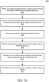
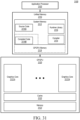
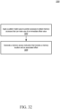
- Graphics processors described herein include support for the use of a global address offset in immediate form in send messages transmitted by a graphics core. Support for an immediate global offset provides a way to encode address increments without requiring the use of add/mov instructions.
- numerous specific details are set forth to provide a more thorough understanding. However, it will be apparent to one of skill in the art that the embodiments described herein may be practiced without one or more of these specific details. In other instances, well-known features have not been described to avoid obscuring the details of the present embodiments.
- FIG. 1 is a block diagram illustrating a computing system 100 configured to implement one or more aspects of the embodiments described herein.
- the computing system 100 includes a processing subsystem 101 having one or more processor(s) 102 and a system memory 104 communicating via an interconnection path that may include a memory hub 105.
- the memory hub 105 may be a separate component within a chipset component or may be integrated within the one or more processor(s) 102.
- the memory hub 105 couples with an I/O subsystem 111 via a communication link 106.
- the I/O subsystem 111 includes an I/O hub 107 that can enable the computing system 100 to receive input from one or more input device(s) 108.
- the processing subsystem 101 includes one or more parallel processor(s) 112 coupled to memory hub 105 via a bus or other communication link 113.
- the communication link 113 may be one of any number of standards-based communication link technologies or protocols, such as, but not limited to PCI Express, or may be a vendor specific communications interface or communications fabric.
- the one or more parallel processor(s) 112 may form a computationally focused parallel or vector processing system that can include a large number of processing cores and/or processing clusters, such as a many integrated core (MIC) processor.
- the one or more parallel processor(s) 112 form a graphics processing subsystem that can output pixels to one of the one or more display device(s) 110A coupled via the I/O hub 107.
- the one or more parallel processor(s) 112 can also include a display controller and display interface (not shown) to enable a direct connection to one or more display device(s) 110B.
- a system storage unit 114 can connect to the I/O hub 107 to provide a storage mechanism for the computing system 100.
- An I/O switch 116 can be used to provide an interface mechanism to enable connections between the I/O hub 107 and other components, such as a network adapter 118 and/or wireless network adapter 119 that may be integrated into the platform, and various other devices that can be added via one or more add-in device(s) 120.
- the add-in device(s) 120 may also include, for example, one or more external graphics processor devices, graphics cards, and/or compute accelerators.
- the network adapter 118 can be an Ethernet adapter or another wired network adapter.
- the wireless network adapter 119 can include one or more of a Wi-Fi, Bluetooth, near field communication (NFC), or other network device that includes one or more wireless radios.
- the computing system 100 can include other components not explicitly shown, including USB or other port connections, optical storage drives, video capture devices, and the like, which may also be connected to the I/O hub 107.
- Communication paths interconnecting the various components in FIG. 1 may be implemented using any suitable protocols, such as PCI (Peripheral Component Interconnect) based protocols (e.g., PCI-Express), or any other bus or point-to-point communication interfaces and/or protocol(s), such as the NVLink high-speed interconnect, Compute Express Link TM (CXL TM ) (e.g., CXL.mem), Infinity Fabric (IF), Ethernet (IEEE 802.3), remote direct memory access (RDMA), InfiniBand, Internet Wide Area RDMA Protocol (iWARP), Transmission Control Protocol (TCP), User Datagram Protocol (UDP), quick UDP Internet Connections (QUIC), RDMA over Converged Ethernet (RoCE), Intel QuickPath Interconnect (QPI), Intel Ultra Path Interconnect (UPI), Intel On
- the one or more parallel processor(s) 112 may incorporate circuitry optimized for graphics and video processing, including, for example, video output circuitry, and constitutes a graphics processing unit (GPU). Alternatively, or additionally, the one or more parallel processor(s) 112 can incorporate circuitry optimized for general purpose processing, while preserving the underlying computational architecture, described in greater detail herein.
- Components of the computing system 100 may be integrated with one or more other system elements on a single integrated circuit.
- the one or more parallel processor(s) 112, memory hub 105, processor(s) 102, and I/O hub 107 can be integrated into a system on chip (SoC) integrated circuit.
- SoC system on chip
- the components of the computing system 100 can be integrated into a single package to form a system in package (SIP) configuration.
- SIP system in package
- at least a portion of the components of the computing system 100 can be integrated into a multi-chip module (MCM), which can be interconnected with other multi-chip modules into a modular computing system.
- connection topology including the number and arrangement of bridges, the number of processor(s) 102, and the number of parallel processor(s) 112, may be modified as desired.
- system memory 104 can be connected to the processor(s) 102 directly rather than through a bridge, while other devices communicate with system memory 104 via the memory hub 105 and the processor(s) 102.
- the parallel processor(s) 112 are connected to the I/O hub 107 or directly to one of the one or more processor(s) 102, rather than to the memory hub 105.
- the I/O hub 107 and memory hub 105 may be integrated into a single chip. It is also possible that two or more sets of processor(s) 102 are attached via multiple sockets, which can couple with two or more instances of the parallel processor(s) 112.
- the memory hub 105 may be referred to as a Northbridge in some architectures, while the I/O hub 107 may be referred to as a Southbridge.
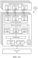
- FIG. 2A illustrates a parallel processor 200.
- the parallel processor 200 may be a GPU, GPGPU or the like as described herein.
- the various components of the parallel processor 200 may be implemented using one or more integrated circuit devices, such as programmable processors, application specific integrated circuits (ASICs), or field programmable gate arrays (FPGA).
- the illustrated parallel processor 200 may be one or more of the parallel processor(s) 112 shown in FIG. 1 .
- the host interface 206 can direct work operations to perform those commands to a front end 208.
- the front end 208 couples with a scheduler 210, which is configured to distribute commands or other work items to a processing cluster array 212.
- the scheduler 210 ensures that the processing cluster array 212 is properly configured and in a valid state before tasks are distributed to the processing clusters of the processing cluster array 212.
- the scheduler 210 may be implemented via firmware logic executing on a microcontroller.
- the microcontroller implemented scheduler 210 is configurable to perform complex scheduling and work distribution operations at coarse and fine granularity, enabling rapid preemption and context switching of threads executing on the processing cluster array 212.
- the host software can prove workloads for scheduling on the processing cluster array 212 via one of multiple graphics processing doorbells.
- polling for new workloads or interrupts can be used to identify or indicate availability of work to perform.
- the workloads can then be automatically distributed across the processing cluster array 212 by the scheduler 210 logic within the scheduler microcontroller.
- the processing cluster array 212 can include up to "N" processing clusters (e.g., cluster 214A, cluster 214B, through cluster 214N). Each cluster 214A-214N of the processing cluster array 212 can execute a large number of concurrent threads.
- the scheduler 210 can allocate work to the clusters 214A-214N of the processing cluster array 212 using various scheduling and/or work distribution algorithms, which may vary depending on the workload arising for each type of program or computation. The scheduling can be handled dynamically by the scheduler 210 or can be assisted in part by compiler logic during compilation of program logic configured for execution by the processing cluster array 212.
- different clusters 214A-214N of the processing cluster array 212 can be allocated for processing different types of programs or for performing different types of computations.
- the processing cluster array 212 can be configured to perform various types of parallel processing operations.
- the processing cluster array 212 is configured to perform general-purpose parallel compute operations.
- the processing cluster array 212 can include logic to execute processing tasks including filtering of video and/or audio data, performing modeling operations, including physics operations, and performing data transformations.
- the processing cluster array 212 is configured to perform parallel graphics processing operations.
- the processing cluster array 212 can include additional logic to support the execution of such graphics processing operations, including, but not limited to texture sampling logic to perform texture operations, as well as tessellation logic and other vertex processing logic.
- the processing cluster array 212 can be configured to execute graphics processing related shader programs such as, but not limited to vertex shaders, tessellation shaders, geometry shaders, and pixel shaders.
- the parallel processing unit 202 can transfer data from system memory via the I/O unit 204 for processing. During processing the transferred data can be stored to on-chip memory (e.g., parallel processor memory 222) during processing, then written back to system memory.
- the processing cluster array 212 can receive processing tasks to be executed via the scheduler 210, which receives commands defining processing tasks from front end 208.
- processing tasks can include indices of data to be processed, e.g., surface (patch) data, primitive data, vertex data, and/or pixel data, as well as state parameters and commands defining how the data is to be processed (e.g., what program is to be executed).
- the scheduler 210 may be configured to fetch the indices corresponding to the tasks or may receive the indices from the front end 208.
- the front end 208 can be configured to ensure the processing cluster array 212 is configured to a valid state before the workload specified by incoming command buffers (e.g., batch-buffers, push buffers, etc.) is initiated.
- incoming command buffers e.g., batch-buffers, push buffers, etc.
- Each of the one or more instances of the parallel processing unit 202 can couple with parallel processor memory 222.
- the parallel processor memory 222 can be accessed via the memory crossbar 216, which can receive memory requests from the processing cluster array 212 as well as the I/O unit 204.
- the memory crossbar 216 can access the parallel processor memory 222 via a memory interface 218.
- the memory interface 218 can include multiple partition units (e.g., partition unit 220A, partition unit 220B, through partition unit 220N) that can each couple to a portion (e.g., memory unit) of parallel processor memory 222.
- the memory units 224A-224N can include various types of memory devices, including dynamic random-access memory (DRAM) or graphics random access memory, such as synchronous graphics random access memory (SGRAM), including graphics double data rate (GDDR) memory.
- DRAM dynamic random-access memory
- SGRAM synchronous graphics random access memory
- GDDR graphics double data rate
- the memory units 224A-224N may also include 3D stacked memory, including but not limited to high bandwidth memory (HBM).
- Render targets such as frame buffers or texture maps may be stored across the memory units 224A-224N, allowing partition units 220A-220N to write portions of each render target in parallel to efficiently use the available bandwidth of parallel processor memory 222.
- a local instance of the parallel processor memory 222 may be excluded in favor of a unified memory design that utilizes system memory in conjunction with local cache memory.
- any one of the clusters 214A-214N of the processing cluster array 212 has the ability to process data that will be written to any of the memory units 224A-224N within parallel processor memory 222.
- the memory crossbar 216 can be configured to transfer the output of each cluster 214A-214N to any partition unit 220A-220N or to another cluster 214A-214N, which can perform additional processing operations on the output.
- Each cluster 214A-214N can communicate with the memory interface 218 through the memory crossbar 216 to read from or write to various external memory devices.
- the memory crossbar 216 has a connection to the memory interface 218 to communicate with the I/O unit 204, as well as a connection to a local instance of the parallel processor memory 222, enabling the processing units within the different processing clusters 214A-214N to communicate with system memory or other memory that is not local to the parallel processing unit 202.
- the memory crossbar 216 may, for example, be able to use virtual channels to separate traffic streams between the clusters 214A-214N and the partition units 220A-220N.
- the parallel processor 200 can be an add-in device, such as add-in device 120 of FIG. 1 , which may be a graphics card such as a discrete graphics card that includes one or more GPUs, one or more memory devices, and device-to-device or network or fabric interfaces.
- the different instances of the parallel processing unit 202 can be configured to inter-operate even if the different instances have different numbers of processing cores, different amounts of local parallel processor memory, and/or other configuration differences.
- some instances of the parallel processing unit 202 can include higher precision floating point units relative to other instances.
- Systems incorporating one or more instances of the parallel processing unit 202 or the parallel processor 200 can be implemented in a variety of configurations and form factors, including but not limited to desktop, laptop, or handheld personal computers, servers, workstations, game consoles, and/or embedded systems.
- An orchestrator can form composite nodes for workload performance using one or more of: disaggregated processor resources, cache resources, memory resources, storage resources, and networking resources.
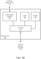
- FIG. 2B is a block diagram of a partition unit 220.
- the partition unit 220 may be an instance of one of the partition units 220A-220N of FIG. 2A .
- the partition unit 220 includes an L2 cache 221, a frame buffer interface 225, and a ROP 226 (raster operations unit).
- the L2 cache 221 is a read/write cache that is configured to perform load and store operations received from the memory crossbar 216 and ROP 226. Read misses and urgent write-back requests are output by L2 cache 221 to frame buffer interface 225 for processing. Updates can also be sent to the frame buffer via the frame buffer interface 225 for processing.
- the frame buffer interface 225 interfaces with one of the memory units in parallel processor memory, such as the memory units 224A-224N of FIG. 2A (e.g., within parallel processor memory 222).
- the partition unit 220 may additionally or alternatively also interface with one of the memory units in parallel processor memory via a memory controller (not shown).
- the ROP 226 is a processing unit that performs raster operations such as stencil, z test, blending, and the like.
- the ROP 226 then outputs processed graphics data that is stored in graphics memory.
- the ROP 226 includes or couples with a CODEC 227 that includes compression logic to compress depth or color data that is written to memory or the L2 cache 221 and decompress depth or color data that is read from memory or the L2 cache 221.
- the compression logic can be lossless compression logic that makes use of one or more of multiple compression algorithms.
- the type of compression that is performed by the CODEC 227 can vary based on the statistical characteristics of the data to be compressed. For example, in one embodiment, delta color compression is performed on depth and color data on a per-tile basis.
- the ROP 226 may be included within each processing cluster (e.g., cluster 214A-214N of FIG. 2A ) instead of within the partition unit 220. In such embodiment, read and write requests for pixel data are transmitted over the memory crossbar 216 instead of pixel fragment data.
- the processed graphics data may be displayed on a display device, such as one of the one or more display device(s) 110A-110B of FIG. 1 , routed for further processing by the processor(s) 102, or routed for further processing by one of the processing entities within the parallel processor 200 of FIG. 2A .
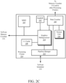
- FIG. 2C is a block diagram of a processing cluster 214 within a parallel processing unit.
- the processing cluster is an instance of one of the processing clusters 214A-214N of FIG. 2A .
- the processing cluster 214 can be configured to execute many threads in parallel, where the term "thread” refers to an instance of a particular program executing on a particular set of input data.
- SIMD single-instruction, multiple-data
- SIMT single-instruction, multiple-thread
- Operation of the processing cluster 214 can be controlled via a pipeline manager 232 that distributes processing tasks to SIMT parallel processors.
- the pipeline manager 232 receives instructions from the scheduler 210 of FIG. 2A and manages execution of those instructions via a graphics multiprocessor 234 and/or a texture unit 236.
- the illustrated graphics multiprocessor 234 is an exemplary instance of a SIMT parallel processor. However, various types of SIMT parallel processors of differing architectures may be included within the processing cluster 214.
- One or more instances of the graphics multiprocessor 234 can be included within a processing cluster 214.
- the graphics multiprocessor 234 can process data and a data crossbar 240 can be used to distribute the processed data to one of multiple possible destinations, including other shader units.
- the pipeline manager 232 can facilitate the distribution of processed data by specifying destinations for processed data to be distributed via the data crossbar 240.
- the graphics multiprocessor 234 may include an internal cache memory to perform load and store operations.
- the graphics multiprocessor 234 can forego an internal cache and use a cache memory (e.g., level 1 (LI) cache 248) within the processing cluster 214.
- Each graphics multiprocessor 234 also has access to level 2 (L2) caches within the partition units (e.g., partition units 220A-220N of FIG. 2A ) that are shared among all processing clusters 214 and may be used to transfer data between threads.
- L2 (L2) caches within the partition units (e.g., partition units 220A-220N of FIG. 2A ) that are shared among all processing clusters 214 and may be used to transfer data between threads.
- the graphics multiprocessor 234 may also access off-chip global memory, which can include one or more of local parallel processor memory and/or system memory. Any memory external to the parallel processing unit 202 may be used as global memory.
- the processing cluster 214 includes multiple instances of the graphics multiprocessor 234 can
- Each processing cluster 214 may include an MMU 245 (memory management unit) that is configured to map virtual addresses into physical addresses.
- MMU 245 memory management unit
- the MMU 245 includes a set of page table entries (PTEs) used to map a virtual address to a physical address of a tile and optionally a cache line index.
- PTEs page table entries
- the MMU 245 may include address translation lookaside buffers (TLB) or caches that may reside within the graphics multiprocessor 234 or the L1 cache 248 of processing cluster 214.
- TLB address translation lookaside buffers
- the physical address is processed to distribute surface data access locality to allow efficient request interleaving among partition units.
- the cache line index may be used to determine whether a request for a cache line is a hit or miss.
- a processing cluster 214 may be configured such that each graphics multiprocessor 234 is coupled to a texture unit 236 for performing texture mapping operations, e.g., determining texture sample positions, reading texture data, and filtering the texture data.
- Texture data is read from an internal texture L1 cache (not shown) or in some embodiments from the L1 cache within graphics multiprocessor 234 and is fetched from an L2 cache, local parallel processor memory, or system memory, as needed.
- Each graphics multiprocessor 234 outputs processed tasks to the data crossbar 240 to provide the processed task to another processing cluster 214 for further processing or to store the processed task in an L2 cache, local parallel processor memory, or system memory via the memory crossbar 216.
- the instruction cache 252 may receive a stream of instructions to execute from the pipeline manager 232.
- the instructions are cached in the instruction cache 252 and dispatched for execution by the instruction unit 254.
- the instruction unit 254 can dispatch instructions as thread groups (e.g., warps), with each thread of the thread group assigned to a different execution unit within GPGPU core 262.
- An instruction can access any of a local, shared, or global address space by specifying an address within a unified address space.
- the address mapping unit 256 can be used to translate addresses in the unified address space into a distinct memory address that can be accessed by the load/store units 266.
- the register file 258 provides a set of registers for the functional units of the graphics multiprocessor 234.
- the register file 258 provides temporary storage for operands connected to the data paths of the functional units (e.g., GPGPU cores 262, load/store units 266) of the graphics multiprocessor 234.
- the register file 258 may be divided between each of the functional units such that each functional unit is allocated a dedicated portion of the register file 258. For example, the register file 258 may be divided between the different warps being executed by the graphics multiprocessor 234.
- the GPGPU cores 262 can each include floating point units (FPUs) and/or integer arithmetic logic units (ALUs) that are used to execute instructions of the graphics multiprocessor 234.
- the GPGPU cores 262 can include hardware logic that may otherwise reside within the tensor and/or ray-tracing cores 263.
- the GPGPU cores 262 can be similar in architecture or can differ in architecture. For example, and in one embodiment, a first portion of the GPGPU cores 262 include a single precision FPU and an integer ALU while a second portion of the GPGPU cores include a double precision FPU.
- the FPUs can implement the IEEE 754-2008 standard for floating point arithmetic or enable variable precision floating point arithmetic.
- the graphics multiprocessor 234 can additionally include one or more fixed function or special function units to perform specific functions such as copy rectangle or pixel blending operations.
- One or more of the GPGPU cores can also include fixed or special function logic.
- the GPGPU cores 262 may include SIMD logic capable of performing a single instruction on multiple sets of data.
- GPGPU cores 262 can physically execute SIMD4, SIMD8, and SIMD16 instructions and logically execute SIMD1, SIMD2, and SIMD32 instructions.
- the SIMD instructions for the GPGPU cores can be generated at compile time by a shader compiler or automatically generated when executing programs written and compiled for single program multiple data (SPMD) or SIMT architectures. Multiple threads of a program configured for the SIMT execution model can be executed via a single SIMD instruction. For example, and in one embodiment, eight SIMT threads that perform the same or similar operations can be executed in parallel via a single SIMD8 logic unit.
- the cache memory 272 can be used as a data cache for example, to cache texture data communicated between the functional units and the texture unit 236.
- the shared memory 270 can also be used as a program managed cached.
- the shared memory 270 and the cache memory 272 can couple with the data crossbar 240 to enable communication with other components of the processing cluster. Threads executing on the GPGPU cores 262 can programmatically store data within the shared memory in addition to the automatically cached data that is stored within the cache memory 272.
- the graphics multiprocessor 325 of FIG. 3A includes multiple additional instances of execution resource units relative to the graphics multiprocessor 234 of FIG. 2D .
- the graphics multiprocessor 325 can include multiple instances of the instruction unit 332A-332B, register file 334A-334B, and texture unit(s) 344A-344B.
- the graphics multiprocessor 325 also includes multiple sets of graphics or compute execution units (e.g., GPGPU core 336A-336B, tensor core 337A-337B, ray-tracing core 338A-338B) and multiple sets of load/store units 340A-340B.
- the execution resource units have a common instruction cache 330, texture and/or data cache memory 342, and shared memory 346.
- the parallel processor or GPGPU as described herein may be communicatively coupled to host/processor cores to accelerate graphics operations, machine-learning operations, pattern analysis operations, and various general-purpose GPU (GPGPU) functions.
- the GPU may be communicatively coupled to the host processor/cores over a bus or other interconnect (e.g., a high-speed interconnect such as PCIe, NVLink, or other known protocols, standardized protocols, or proprietary protocols).
- the GPU may be integrated on the same package or chip as the cores and communicatively coupled to the cores over an internal processor bus/interconnect (i.e., internal to the package or chip).
- the processor cores may allocate work to the GPU in the form of sequences of commands/instructions contained in a work descriptor.
- the GPU then uses dedicated circuitry/logic for efficiently processing these commands/instructions.
- a multi-core group 365A may include a set of graphics cores 370, a set of tensor cores 371, and a set of ray tracing cores 372.
- a scheduler/dispatcher 368 schedules and dispatches the graphics threads for execution on the various cores 370, 371, 372.
- a set of register files 369 store operand values used by the cores 370, 371, 372 when executing the graphics threads. These may include, for example, integer registers for storing integer values, floating point registers for storing floating point values, vector registers for storing packed data elements (integer and/or floating-point data elements) and tile registers for storing tensor/matrix values.
- the tile registers may be implemented as combined sets of vector registers.
- One or more combined level 1 (LI) caches and shared memory units 373 store graphics data such as texture data, vertex data, pixel data, ray data, bounding volume data, etc., locally within each multi-core group 365A.
- One or more texture units 374 can also be used to perform texturing operations, such as texture mapping and sampling.
- a Level 2 (L2) cache 375 shared by all or a subset of the multi-core groups 365A-365N stores graphics data and/or instructions for multiple concurrent graphics threads. As illustrated, the L2 cache 375 may be shared across a plurality of multi-core groups 365A-365N.
- One or more memory controllers 367 couple the GPU 380 to a memory 366 which may be a system memory (e.g., DRAM) and/or a dedicated graphics memory (e.g., GDDR6 memory).
- I/O circuitry 363 couples the GPU 380 to one or more I/O devices 362 such as digital signal processors (DSPs), network controllers, or user input devices.
- I/O devices 362 such as digital signal processors (DSPs), network controllers, or user input devices.
- An on-chip interconnect may be used to couple the I/O devices 362 to the GPU 380 and memory 366.
- IOMMUs I/O memory management units
- the IOMMU 364 manages multiple sets of page tables to map virtual addresses to physical addresses in system memory 366.
- the I/O devices 362, CPU(s) 361, and GPU(s) 380 may then share the same virtual address space.
- each of the cores 370, 371, 372 and/or multi-core groups 365A-365N may include translation lookaside buffers (TLBs) to cache guest virtual to guest physical translations, guest physical to host physical translations, and guest virtual to host physical translations.
- TLBs translation lookaside buffers
- the tensor cores 371 may include a plurality of execution units specifically designed to perform matrix operations, which are the fundamental compute operation used to perform deep learning operations. For example, simultaneous matrix multiplication operations may be used for neural network training and inferencing.
- the tensor cores 371 may perform matrix processing using a variety of operand precisions including single precision floating-point (e.g., 32 bits), half-precision floating point (e.g., 16 bits), integer words (16 bits), bytes (8 bits), and half-bytes (4 bits).
- a neural network implementation extracts features of each rendered scene, potentially combining details from multiple frames, to construct a high-quality final image.
- parallel matrix multiplication work may be scheduled for execution on the tensor cores 371.
- the training of neural networks requires a significant number of matrix dot product operations.
- the tensor cores 371 may include at least N dot-product processing elements. Before the matrix multiply begins, one entire matrix is loaded into tile registers and at least one column of a second matrix is loaded each cycle for N cycles. Each cycle, there are N dot products that are processed.
- a non-zero value can be loaded from the compressed and/or encoded representation of at least a portion of matrix A. Based on the location in matrix A for the non-zero value, which may be determined from index or coordinate metadata associated with the non-zero value, a corresponding value in input matrix B may be loaded. Depending on the operation to be performed (e.g., multiply), the load of the value from input matrix B may be bypassed if the corresponding value is a zero value.
- the pairings of values for certain operations, such as multiply operations may be pre-scanned by scheduler logic and only operations between non-zero inputs are scheduled.
- the ray tracing cores 372 perform traversal and intersection operations in concert with the image denoising techniques described herein, at least a portion of which may be executed on the tensor cores 371.
- the tensor cores 371 may implement a deep learning neural network to perform denoising of frames generated by the ray tracing cores 372.
- the CPU(s) 361, graphics cores 370, and/or ray tracing cores 372 may also implement all or a portion of the denoising and/or deep learning algorithms.
- the ray tracing cores 372 may process all BVH traversal and/or ray-primitive intersections, saving the graphics cores 370 from being overloaded with thousands of instructions per ray.
- each ray tracing core 372 includes a first set of specialized circuitry for performing bounding box tests (e.g., for traversal operations) and/or a second set of specialized circuitry for performing the ray-triangle intersection tests (e.g., intersecting rays which have been traversed).
- a hybrid rasterization/ray tracing approach is used in which work is distributed between the graphics cores 370 and ray tracing cores 372.
- the ray tracing cores 372 may include hardware support for a ray tracing instruction set such as Microsoft's DirectX Ray Tracing (DXR) which includes a DispatchRays command, as well as ray-generation, closest-hit, any-hit, and miss shaders, which enable the assignment of unique sets of shaders and textures for each object.
- DXR DirectX Ray Tracing
- Another ray tracing platform which may be supported by the ray tracing cores 372, graphics cores 370 and tensor cores 371 is Vulkan 1.1.85. Note, however, that the underlying principles described herein are not limited to any particular ray tracing ISA.
- processor 407 includes 24 cores, each with its own L1 cache, twelve shared L2 caches, and twelve shared L3 caches. In this embodiment, one of the L2 and L3 caches are shared by two adjacent cores.
- the processor 407 and the graphics accelerator integration module 446 connect with system memory 441, which may include processor memories 401-402.
- proxy circuit 425 which takes part in the cache coherency mechanism on behalf of cache 438 and memories 433-434, M (e.g., sending updates to the cache 438 related to modifications/accesses of cache lines on processor caches 462A-462D, 456 and receiving updates from the cache 438).
- any host processor can address these resources directly using an effective address value.
- One optional function of the accelerator integration circuit 436 is the physical separation of the graphics processing engines 431-432, N so that they appear to the system as independent units.
- the graphics acceleration module 446 and/or the individual graphics processing engines 431-432, N can be shared by all or a subset of the processes in the system.
- the technologies described herein may include an infrastructure for setting up the process state and sending a WD 484 to a graphics acceleration module 446 to start a job in a virtualized environment.
- the dedicated-process programming model is implementation-specific.
- a single process owns the graphics acceleration module 446 or an individual graphics processing engine 431. Because the graphics acceleration module 446 is owned by a single process, the hypervisor initializes the accelerator integration circuit 436 for the owning partition and the operating system initializes the accelerator integration circuit 436 for the owning process at the time when the graphics acceleration module 446 is assigned.
- Each WD 484 may be specific to a particular graphics acceleration module 446 and/or graphics processing engine 431-432, N. It contains all the information a graphics processing engine 431-432, N requires to do its work, or it can be a pointer to a memory location where the application has set up a command queue of work to be completed.
- the shared programming models allow for all or a subset of processes from all or a subset of partitions in the system to use a graphics acceleration module 446.
- the system hypervisor 496 owns the graphics acceleration module 446 and makes its function available to all operating systems 495.
- the graphics acceleration module 446 may adhere to the following requirements: 1) An application's job request must be autonomous (that is, the state does not need to be maintained between jobs), or the graphics acceleration module 446 must provide a context save and restore mechanism. 2) An application's job request is guaranteed by the graphics acceleration module 446 to complete in a specified amount of time, including any translation faults, or the graphics acceleration module 446 provides the ability to preempt the processing of the job. 3) The graphics acceleration module 446 must be guaranteed fairness between processes when operating in the directed shared programming model.
- the AMR value is the AMR state to use for the current process.
- the value passed to the operating system is similar to an application setting the AMR. If the accelerator integration circuit 436 and graphics acceleration module 446 implementations do not support a User Authority Mask Override Register (UAMOR), the operating system may apply the current UAMOR value to the AMR value before passing the AMR in the hypervisor call.
- the hypervisor 496 may optionally apply the current Authority Mask Override Register (AMOR) value before placing the AMR into the process element 483.
- the CSRP may be one of the registers 445 containing the effective address of an area in the application's address space 482 for the graphics acceleration module 446 to save and restore the context state. This pointer is optional if no state is required to be saved between jobs or when a job is preempted.
- the context save/restore area may be pinned system memory.
- the hypervisor may initialize a plurality of accelerator integration slice 490 registers 445.
- the GPU-attached memory 420-423 may be mapped as part of system memory and accessed using shared virtual memory (SVM) technology, but without suffering the typical performance drawbacks associated with full system cache coherence.
- SVM shared virtual memory
- the ability to GPU-attached memory 420-423 to be accessed as system memory without onerous cache coherence overhead provides a beneficial operating environment for GPU offload.
- This arrangement allows the host processor 405 software to setup operands and access computation results, without the overhead of tradition I/O DMA data copies. Such traditional copies involve driver calls, interrupts and memory mapped I/O (MMIO) accesses that are all inefficient relative to simple memory accesses.
- MMIO memory mapped I/O
- the ability to access GPU attached memory 420-423 without cache coherence overheads can be critical to the execution time of an offloaded computation.
- cache coherence overhead can significantly reduce the effective write bandwidth seen by a GPU 410-413.
- the efficiency of operand setup, the efficiency of results access, and the efficiency of GPU computation all play a role in determining the effectiveness of GPU offload.
- the bias table entry associated with each access to the GPU-attached memory 420-423 is accessed prior the actual access to the GPU memory, causing the following operations.
- First, local requests from the GPU 410-413 that find their page in GPU bias are forwarded directly to a corresponding GPU memory 420-423.
- Local requests from the GPU that find their page in host bias are forwarded to the processor 405 (e.g., over a high-speed link as discussed above).
- requests from the processor 405 that find the requested page in host processor bias complete the request like a normal memory read.
- requests directed to a GPU-biased page may be forwarded to the GPU 410-413. The GPU may then transition the page to a host processor bias if it is not currently using the page.
- One mechanism for changing the bias state employs an API call (e.g., OpenCL), which, in turn, calls the GPU's device driver which, in turn, sends a message (or enqueues a command descriptor) to the GPU directing it to change the bias state and, for some transitions, perform a cache flushing operation in the host.
- the cache flushing operation is required for a transition from host processor 405 bias to GPU bias but is not required for the opposite transition.
- the graphics processing pipeline 500 may also be implemented using dedicated processing units for one or more functions. It is also possible that one or more portions of the graphics processing pipeline 500 are performed by parallel processing logic within a general-purpose processor (e.g., CPU). Optionally, one or more portions of the graphics processing pipeline 500 can access on-chip memory (e.g., parallel processor memory 222 as in FIG. 2A ) via a memory interface 528, which may be an instance of the memory interface 218 of FIG. 2A .
- the graphics processor pipeline 500 may also be implemented via a multi-core group 365A as in FIG. 3C .
- a first instance of a primitive assembler 506 receives vertex attributes from the vertex processing unit 504.
- the primitive assembler 506 readings stored vertex attributes as needed and constructs graphics primitives for processing by tessellation control processing unit 508.
- the graphics primitives include triangles, line segments, points, patches, and so forth, as supported by various graphics processing application programming interfaces (APIs).
- a tessellation unit 510 is configured to receive the tessellation factors for edges of a patch and to tessellate the patch into multiple geometric primitives such as line, triangle, or quadrilateral primitives, which are transmitted to a tessellation evaluation processing unit 512.
- the tessellation evaluation processing unit 512 operates on parameterized coordinates of the subdivided patch to generate a surface representation and vertex attributes for each vertex associated with the geometric primitives.
- a second instance of a primitive assembler 514 receives vertex attributes from the tessellation evaluation processing unit 512, reading stored vertex attributes as needed, and constructs graphics primitives for processing by the geometry processing unit 516.
- the geometry processing unit 516 is a programmable execution unit that executes geometry shader programs to transform graphics primitives received from primitive assembler 514 as specified by the geometry shader programs.
- the geometry processing unit 516 may be programmed to subdivide the graphics primitives into one or more new graphics primitives and calculate parameters used to rasterize the new graphics primitives.
- the rasterizer 522 can perform depth culling and other depth-based optimizations.
- the rasterizer 522 also performs scan conversion on the new graphics primitives to generate fragments and output those fragments and associated coverage data to the fragment/pixel processing unit 524.
- the fragment/pixel processing unit 524 is a programmable execution unit that is configured to execute fragment shader programs or pixel shader programs.
- the fragment/pixel processing unit 524 transforming fragments or pixels received from rasterizer 522, as specified by the fragment or pixel shader programs.
- the fragment/pixel processing unit 524 may be programmed to perform operations included but not limited to texture mapping, shading, blending, texture correction and perspective correction to produce shaded fragments or pixels that are output to a raster operations unit 526.
- the fragment/pixel processing unit 524 can read data that is stored in either the parallel processor memory or the system memory for use when processing the fragment data.
- Fragment or pixel shader programs may be configured to shade at sample, pixel, tile, or other granularities depending on the sampling rate configured for the processing units.
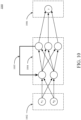
- An exemplary type of machine learning algorithm is a neural network.
- a simple type of neural network is a feedforward network.
- a feedforward network may be implemented as an acyclic graph in which the nodes are arranged in layers.
- a feedforward network topology includes an input layer and an output layer that are separated by at least one hidden layer.
- the hidden layer transforms input received by the input layer into a representation that is useful for generating output in the output layer.
- the network nodes are fully connected via edges to the nodes in adjacent layers, but there are no edges between nodes within each layer.
- the GPGPU 700 includes memory 714A-714B coupled with the processing clusters 706A-706H via a set of memory controllers 712A-712B.
- the memory 714A-714B can include various types of memory devices including dynamic random-access memory (DRAM) or graphics random access memory, such as synchronous graphics random access memory (SGRAM), including graphics double data rate (GDDR) memory.
- DRAM dynamic random-access memory
- SGRAM synchronous graphics random access memory
- GDDR graphics double data rate
- the memory 714A-714B may also include 3D stacked memory, including but not limited to high bandwidth memory (HBM).
- HBM high bandwidth memory
- Multiple instances of the GPGPU 700 can be configured to operate as a compute cluster.
- the communication mechanism used by the compute cluster for synchronization and data exchange varies across embodiments.
- the multiple instances of the GPGPU 700 communicate over the host interface 702.
- the GPGPU 700 includes an I/O hub 709 that couples the GPGPU 700 with a GPU link 710 that enables a direct connection to other instances of the GPGPU.
- the GPU link 710 may be coupled to a dedicated GPU-to-GPU bridge that enables communication and synchronization between multiple instances of the GPGPU 700.
- the GPU link 710 couples with a high-speed interconnect to transmit and receive data to other GPGPUs or parallel processors.
- the GPGPUs 806A-806D connect to the processor 802 via the host interface switch 804, the processor 802 may alternatively include direct support for the P2P GPU links 816 and connect directly to the GPGPUs 806A-806D.
- the P2P GPU link 816 enable the multi-GPU computing system 800 to operate as a single logical GPU.
- the computing architecture described herein can be configured to perform the types of parallel processing that is particularly suited for training and deploying neural networks for machine learning.
- a neural network can be generalized as a network of functions having a graph relationship. As is well-known in the art, there are a variety of types of neural network implementations used in machine learning.
- One exemplary type of neural network is the feedforward network, as previously described.
- Convolution is a specialized kind of mathematical operation performed by two functions to produce a third function that is a modified version of one of the two original functions.
- the first function to the convolution can be referred to as the input, while the second function can be referred to as the convolution kernel.
- the output may be referred to as the feature map.
- the input to a convolution layer can be a multidimensional array of data that defines the various color components of an input image.
- the convolution kernel can be a multidimensional array of parameters, where the parameters are adapted by the training process for the neural network.
- the convolutional layers are sparsely connected, which differs from traditional neural network configuration found in the fully connected layers 908.
- Traditional neural network layers are fully connected, such that every output unit interacts with every input unit.
- the convolutional layers are sparsely connected because the output of the convolution of a field is input (instead of the respective state value of each of the nodes in the field) to the nodes of the subsequent layer, as illustrated.
- the kernels associated with the convolutional layers perform convolution operations, the output of which is sent to the next layer.
- the dimensionality reduction performed within the convolutional layers is one aspect that enables the CNN to scale to process large images.
- FIG. 11 illustrates training and deployment of a deep neural network.
- the neural network is trained using a training dataset 1102.
- Various training frameworks 1104 have been developed to enable hardware acceleration of the training process.
- the machine learning framework 604 of FIG. 6 may be configured as a training framework 1104.
- the training framework 1104 can hook into an untrained neural network 1106 and enable the untrained neural net to be trained using the parallel processing resources described herein to generate a trained neural network 1108.
- model parallelism 1202 different computational nodes in a distributed system can perform training computations for different parts of a single network. For example, each layer of a neural network can be trained by a different processing node of the distributed system.
- the benefits of model parallelism include the ability to scale to particularly large models. Splitting the computations associated with different layers of the neural network enables the training of very large neural networks in which the weights of all layers would not fit into the memory of a single computational node. In some instances, model parallelism can be particularly useful in performing unsupervised training of large neural networks.
- Distributed training has increased overhead relative to training on a single machine.
- the parallel processors and GPGPUs described herein can each implement various techniques to reduce the overhead of distributed training, including techniques to enable high bandwidth GPU-to-GPU data transfer and accelerated remote data synchronization.
- FIG. 12B is a block diagram illustrating a programmable network interface 1210 and data processing unit.
- the programmable network interface 1210 is a programmable network engine that can be used to accelerate network-based compute tasks within a distributed environment.
- the programmable network interface 1210 can couple with a host system via host interface 1270.
- the programmable network interface 1210 can be used to accelerate network or storage operations for CPUs or GPUs of the host system.
- the host system can be, for example, a node of a distributed learning system used to perform distributed training, for example, as shown in FIG. 12A .
- the host system can also be a data center node within a data center.
- access to remote storage containing model data can be accelerated by the programmable network interface 1210.
- the programmable network interface 1210 can be configured to present remote storage devices as local storage devices to the host system.
- the programmable network interface 1210 can also accelerate remote direct memory access (RDMA) operations performed between GPUs of the host system with GPUs of remote systems.
- RDMA remote direct memory access
- the programmable network interface 1210 can enable storage functionality such as, but not limited to NVME-oF.
- the programmable network interface 1210 can also accelerate encryption, data integrity, compression, and other operations for remote storage on behalf of the host system, allowing remote storage to approach the latencies of storage devices that are directly attached to the host system.
- Training platforms are generally highly parallel and include optimizations to accelerate multi-GPU single node training and multi-node, multi-GPU training.
- Exemplary parallel processors suited for training include the general-purpose graphics processing unit 700 of FIG. 7 and the multi-GPU computing system 800 of FIG. 8 .
- deployed machine learning platforms generally include lower power parallel processors suitable for use in products such as cameras, autonomous robots, and autonomous vehicles.
- the media processor 1302 and vision processor 1304 can work in concert to accelerate computer vision operations.
- the media processor 1302 can enable low latency decode of multiple high-resolution (e.g., 4K, 8K) video streams.
- the decoded video streams can be written to a buffer in the on-chip memory 1305.
- the vision processor 1304 can then parse the decoded video and perform preliminary processing operations on the frames of the decoded video in preparation of processing the frames using a trained image recognition model.
- the vision processor 1304 can accelerate convolution operations for a CNN that is used to perform image recognition on the high-resolution video data, while back-end model computations are performed by the GPGPU 1306.
- the multi-core processor 1308 can include control logic to assist with sequencing and synchronization of data transfers and shared memory operations performed by the media processor 1302 and the vision processor 1304.
- the multi-core processor 1308 can also function as an application processor to execute software applications that can make use of the inferencing compute capability of the GPGPU 1306. For example, at least a portion of the navigation and driving logic can be implemented in software executing on the multi-core processor 1308. Such software can directly issue computational workloads to the GPGPU 1306, or the computational workloads can be issued to the multi-core processor 1308, which can offload at least a portion of those operations to the GPGPU 1306.
- the GPGPU 1306 can include compute clusters such as a low power configuration of the processing clusters 706A-706H within general-purpose graphics processing unit 700.
- the compute clusters within the GPGPU 1306 can support instruction that are specifically optimized to perform inferencing computations on a trained neural network.
- the GPGPU 1306 can support instructions to perform low precision computations such as 8-bit and 4-bit integer vector operations.
- the system 1400 may be a processing platform incorporated within a system-on-a-chip (SoC) integrated circuit for use in mobile, handheld, or embedded devices such as within Internet-of-things (IoT) devices with wired or wireless connectivity to a local or wide area network.
- SoC system-on-a-chip
- the memory device 1420 can be a dynamic random-access memory (DRAM) device, a static random-access memory (SRAM) device, flash memory device, phase-change memory device, or some other memory device having suitable performance to serve as process memory.
- the memory device 1420 can, for example, operate as system memory for the system 1400, to store data 1422 and instructions 1421 for use when the one or more processors 1402 executes an application or process.
- Memory controller 1416 also couples with an optional external graphics processor 1418, which may communicate with the one or more graphics processors 1408 in processors 1402 to perform graphics and media operations.
- graphics, media, and or compute operations may be assisted by an accelerator 1412 which is a coprocessor that can be configured to perform a specialized set of graphics, media, or compute operations.
- the accelerator 1412 may be a matrix multiplication accelerator used to optimize machine learning or compute operations.
- the accelerator 1412 can be a ray-tracing accelerator that can be used to perform ray-tracing operations in concert with the graphics processor 1408.
- an external accelerator 1419 may be used in place of or in concert with the accelerator 1412.
- Each of processor cores 1502A-1502N includes one or more internal cache units 1504A-1504N.
- each processor core 1502A-1502N also has access to one or more shared cache units 1506.
- the internal cache units 1504A-1504N and shared cache units 1506 represent a cache memory hierarchy within the processor 1500.
- the cache memory hierarchy may include at least one level of instruction and data cache within each processor core and one or more levels of shared mid-level cache, such as a Level 2 (L2), Level 3 (L3), Level 4 (L4), or other levels of cache, where the highest level of cache before external memory is classified as the LLC.
- cache coherency logic maintains coherency between the various cache units 1506 and 1504A-1504N.
- FIG. 15B is a block diagram of hardware logic of a graphics processor core 1519, according to some embodiments described herein.
- the graphics processor core 1519 sometimes referred to as a core slice, can be one or multiple graphics cores within a modular graphics processor.
- the graphics processor core 1519 is exemplary of one graphics core slice, and a graphics processor as described herein may include multiple graphics core slices based on target power and performance envelopes.
- Each graphics processor core 1519 can include a fixed function block 1530 coupled with multiple sub-cores 1521A-1521F, also referred to as sub-slices, that include modular blocks of general-purpose and fixed function logic.
- the fixed function block 1530 may include a geometry/fixed function pipeline 1531 that can be shared by all sub-cores in the graphics processor core 1519, for example, in lower performance and/or lower power graphics processor implementations.
- the geometry/fixed function pipeline 1531 may include a 3D fixed function pipeline (e.g., 3D pipeline 1612 as in FIG. 16A described below) a video front-end unit, a thread spawner and thread dispatcher, and a unified return buffer manager, which manages unified return buffers (e.g., unified return buffer 1718 in FIG. 17 , as described below).
- the graphics processor core 1519 may have more than or fewer than the illustrated sub-cores 1521A-1521F, up to N modular sub-cores.
- the graphics processor core 1519 can also include shared function logic 1535, shared and/or cache memory 1536, a geometry/fixed function pipeline 1537, as well as additional fixed function logic 1538 to accelerate various graphics and compute processing operations.
- the shared function logic 1535 can include logic units associated with the shared function logic 1720 of FIG. 17 (e.g., sampler, math, and/or inter-thread communication logic) that can be shared by each N sub-cores within the graphics processor core 1519.
- the one or more CPU(s) 1546 can write commands into registers or memory in the GPGPU 1570 that has been mapped into an accessible address space.
- the command processors 1557 can read the commands from registers or memory and determine how those commands will be processed within the GPGPU 1570.
- a thread dispatcher 1558 can then be used to dispatch threads to the compute units 1560A-1560N to perform those commands.
- Each compute unit 1560A-1560N can execute threads independently of the other compute units. Additionally, each compute unit 1560A-1560N can be independently configured for conditional computation and can conditionally output the results of computation to memory.
- the command processors 1557 can interrupt the one or more CPU(s) 1546 when the submitted commands are complete.
- the 3D/Media subsystem 1615 may include logic for executing threads spawned by 3D pipeline 1612 and media pipeline 1616.
- the pipelines may send thread execution requests to 3D/Media subsystem 1615, which includes thread dispatch logic for arbitrating and dispatching the various requests to available thread execution resources.
- the execution resources include an array of graphics execution units to process the 3D and media threads.
- the 3D/Media subsystem 1615 may include one or more internal caches for thread instructions and data. Additionally, the 3D/Media subsystem 1615 may also include shared memory, including registers and addressable memory, to share data between threads and to store output data.
- the graphics processing engine cluster 1622 can connect with an on-chip or on-package fabric interconnect 1624.
- the fabric interconnect 1624 includes a network processor, network on a chip (NoC), or another switching processor to enable the fabric interconnect 1624 to act as a packet switched fabric interconnect that switches data packets between components of the graphics processor 1620.
- the fabric interconnect 1624 can enable communication between graphics engine tiles 1610A-1610D and components such as the video codec engine 1606 and one or more copy engines 1604.
- the copy engines 1604 can be used to move data out of, into, and between the memory devices 1626A-1626D and memory that is external to the graphics processor 1620 (e.g., system memory).
- FIG. 16C illustrates a compute accelerator 1630, according to embodiments described herein.
- the compute accelerator 1630 can include architectural similarities with the graphics processor 1620 of FIG. 16B and is optimized for compute acceleration.
- a compute engine cluster 1632 can include a set of compute engine tiles 1640A-1640D that include execution logic that is optimized for parallel or vector-based general-purpose compute operations.
- the compute engine tiles 1640A-1640D may not include fixed function graphics processing logic, although in some embodiments one or more of the compute engine tiles 1640A-1640D can include logic to perform media acceleration.
- the compute engine tiles 1640A-1640D can connect to memory 1626A-1626D via memory interconnects 1625A-1625D.
- the memory 1626A-1626D and memory interconnects 1625A-1625D may be similar technology as in graphics processor 1620 or can be different.
- the graphics compute engine tiles 1640A-1640D can also be interconnected via a set of tile interconnects 1623A-1623F and may be connected with and/or interconnected by a fabric interconnect 1624.
- the compute accelerator 1630 includes a large L3 cache 1636 that can be configured as a device-wide cache.
- the compute accelerator 1630 can also connect to a host processor and memory via a host interface 1628 in a similar manner as the graphics processor 1620 of FIG. 16B .
- the graphics core array 1714 may include execution logic to perform media functions, such as video and/or image processing.
- the execution units may include general-purpose logic that is programmable to perform parallel general-purpose computational operations, in addition to graphics processing operations.
- the general-purpose logic can perform processing operations in parallel or in conjunction with general-purpose logic within the processor core(s) 1407 of FIG. 14 or core 1502A-1502N as in FIG. 15A .
- the graphics core array 1714 may be scalable, such that the array includes a variable number of graphics cores, each having a variable number of execution units based on the target power and performance level of GPE 1710.
- the execution resources may be dynamically scalable, such that execution resources may be enabled or disabled as needed.
- Each execution unit in graphics execution units 1808A-1808N operates on arrays of data elements.
- the number of data elements is the "execution size," or the number of channels for the instruction.
- An execution channel is a logical unit of execution for data element access, masking, and flow control within instructions.
- the number of channels may be independent of the number of physical Arithmetic Logic Units (ALUs), Floating-Point Units (FPUs), or other logic units (e.g., tensor cores, ray tracing cores, etc.) for a particular graphics processor.
- ALUs Arithmetic Logic Units
- FPUs Floating-Point Units
- other logic units e.g., tensor cores, ray tracing cores, etc.
- the graphics execution units 1808A-1808N may support integer and floating-point data types.
- FIG. 18B illustrates exemplary internal details of an execution unit 1808.
- a graphics execution unit 1808 can include an instruction fetch unit 1837, a general register file array (GRF) 1824, an architectural register file array (ARF) 1826, a thread arbiter 1822, a send unit 1830, a branch unit 1832, a set of SIMD floating point units (FPUs) 1834, and optionally a set of dedicated integer SIMD ALUs 1835.
- the GRF 1824 and ARF 1826 includes the set of general register files and architecture register files associated with each simultaneous hardware thread that may be active in the graphics execution unit 1808. Per thread architectural state may be maintained in the ARF 1826, while data used during thread execution is stored in the GRF 1824. The execution state of each thread, including the instruction pointers for each thread, can be held in thread-specific registers in the ARF 1826.
- the graphics execution unit 1808 can co-issue multiple instructions, which may each be different instructions.
- the thread arbiter 1822 of the graphics execution unit 1808 can dispatch the instructions to one of the send unit 1830, branch unit 1832, or SIMD FPU(s) 1834 for execution.
- Each execution thread can access 128 general-purpose registers within the GRF 1824, where each register can store 32 bytes, accessible as a SIMD 8-element vector of 32-bit data elements.
- Each execution unit thread may have access to 4 Kbytes within the GRF 1824, although embodiments are not so limited, and greater or fewer register resources may be provided in other embodiments.
- the graphics execution unit 1808 may include one or more SIMD floating point units (FPU(s)) 1834 to perform floating-point operations.
- the FPU(s) 1834 may also support integer computation.
- the FPU(s) 1834 can SIMD execute up to M number of 32-bit floating-point (or integer) operations, or SIMD execute up to 2M 16-bit integer or 16-bit floating-point operations.
- at least one of the FPU(s) provides extended math capability to support high-throughput transcendental math functions and double precision 64-bit floating-point.
- a set of 8-bit integer SIMD ALUs 1835 may also be present and may be specifically optimized to perform operations associated with machine learning computations.
- the systolic array 1912 includes hardware to accelerate sparse matrix operations. Multiplication operations for sparse regions of input data can be bypassed without sacrificing throughput. Block sparsity within input matrices can be detected and operations having known output values can be bypassed.
- the systolic array 1912 includes hardware to enable operations on sparse data having a compressed representation.
- a compressed representation of a sparse matrix stores non-zero values and metadata that defines the position of the non-zero values within the matrix.
- Exemplary compressed representations include but are not limited to compressed tensor representations such as compressed sparse row (CSR), compressed sparse column (CSC), compressed sparse fiber (CSF) representations.
- the graphics processor execution units as described herein may natively support instructions in a 128-bit instruction format 2010.
- a 64-bit compacted instruction format 2030 is available for some instructions based on the selected instruction, instruction options, and number of operands.
- the native 128-bit instruction format 2010 provides access to all instruction options, while some options and operations are restricted in the 64-bit format 2030.
- the native instructions available in the 64-bit format 2030 vary by embodiment.
- the instruction is compacted in part using a set of index values in an index field 2013.
- the execution unit hardware references a set of compaction tables based on the index values and uses the compaction table outputs to reconstruct a native instruction in the 128-bit instruction format 2010. Other sizes and formats of instruction can be used.
- the address mode portion of the access/address mode field 2026 may determine whether the instruction is to use direct or indirect addressing. When direct register addressing mode is used bits in the instruction directly provide the register address of one or more operands. When indirect register addressing mode is used, the register address of one or more operands may be computed based on an address register value and an address immediate field in the instruction.
- a geometry pipeline 2120 may include tessellation components to perform hardware-accelerated tessellation of 3D objects.
- a programmable hull shader 2111 may configure the tessellation operations.
- a programmable domain shader 2117 may provide back-end evaluation of tessellation output.
- a tessellator 2113 may operate at the direction of hull shader 2111 and contain special purpose logic to generate a set of detailed geometric objects based on a coarse geometric model that is provided as input to geometry pipeline 2120.
- tessellation components e.g., hull shader 2111, tessellator 2113, and domain shader 2117
- the tessellation components can operate based on data received from the vertex shader 2107.
- the graphics processor 2100 has an interconnect bus, interconnect fabric, or some other interconnect mechanism that allows data and message passing amongst the major components of the processor.
- execution units 2152A-2152B and associated logic units e.g., L1 cache 2151, sampler 2154, texture cache 2158, etc.
- a sampler 2154, caches 2151, 2158 and execution units 2152A-2152B each may have separate memory access paths.
- the texture cache 2158 can also be configured as a sampler cache.
- the geometry pipeline 2120 and media pipeline 2130 maybe configurable to perform operations based on multiple graphics and media programming interfaces and are not specific to any one application programming interface (API).
- a driver software for the graphics processor may translate API calls that are specific to a particular graphics or media library into commands that can be processed by the graphics processor.
- Support may be provided for the Open Graphics Library (OpenGL), Open Computing Language (OpenCL), and/or Vulkan graphics and compute API, all from the Khronos Group.
- Support may also be provided for the Direct3D library from the Microsoft Corporation. A combination of these libraries may be supported.
- Support may also be provided for the Open Source Computer Vision Library (OpenCV).
- OpenCV Open Source Computer Vision Library
- a future API with a compatible 3D pipeline would also be supported if a mapping can be made from the pipeline of the future API to the pipeline of the graphics processor.
- the graphics processor command sequence 2210 may begin with a pipeline flush command 2212 to cause any active graphics pipeline to complete the currently pending commands for the pipeline.
- a pipeline flush command 2212 is performed to cause the active graphics pipeline to complete any pending commands.
- the command parser for the graphics processor will pause command processing until the active drawing engines complete pending operations and the relevant read caches are invalidated.
- any data in the render cache that is marked 'dirty' can be flushed to memory.
- Pipeline flush command 2212 can be used for pipeline synchronization or before placing the graphics processor into a low power state.
- the commands to configure the 3D pipeline state 2230 include 3D state setting commands for vertex buffer state, vertex element state, constant color state, depth buffer state, and other state variables that are to be configured before 3D primitive commands are processed. The values of these commands are determined at least in part based on the particular 3D API in use.
- the 3D pipeline state 2230 commands may also be able to selectively disable or bypass certain pipeline elements if those elements will not be used.
- the graphics processor command sequence 2210 may follow the media pipeline 2224 path when performing media operations.
- the specific use and manner of programming for the media pipeline 2224 depends on the media or compute operations to be performed.
- Specific media decode operations may be offloaded to the media pipeline during media decode.
- the media pipeline can also be bypassed and media decode can be performed in whole or in part using resources provided by one or more general-purpose processing cores.
- the media pipeline may also include elements for general-purpose graphics processor unit (GPGPU) operations, where the graphics processor is used to perform SIMD vector operations using computational shader programs that are not explicitly related to the rendering of graphics primitives.
- GPGPU general-purpose graphics processor unit
- FIG. 23 illustrates an exemplary graphics software architecture for a data processing system 2300.
- a software architecture may include a 3D graphics application 2310, an operating system 2320, and at least one processor 2330.
- Processor 2330 may include a graphics processor 2332 and one or more general-purpose processor core(s) 2334.
- the processor 2330 may be a variant of the processor 1402 or any other of the processors described herein.
- the processor 2330 may be used in place of the processor 1402 or any other of the processors described herein. Therefore, the disclosure of any features in combination with the processor 1402 or any other of the processors described herein also discloses a corresponding combination with the graphics processor 2332 but is not limited to such.
- One or more aspects may be implemented by representative code stored on a machine-readable medium which represents and/or defines logic within an integrated circuit such as a processor.
- the machine-readable medium may include instructions which represent various logic within the processor. When read by a machine, the instructions may cause the machine to fabricate the logic to perform the techniques described herein.
- Such representations known as "IP cores," are reusable units of logic for an integrated circuit that may be stored on a tangible, machine-readable medium as a hardware model that describes the structure of the integrated circuit.
- the hardware model may be supplied to various customers or manufacturing facilities, which load the hardware model on fabrication machines that manufacture the integrated circuit.
- the integrated circuit may be fabricated such that the circuit performs operations described in association with any of the embodiments described herein.
- FIG. 24C illustrates a package assembly 2490 that includes multiple units of hardware logic chiplets connected to a substrate 2480 (e.g., base die).
- a graphics processing unit, parallel processor, and/or compute accelerator as described herein can be composed from diverse silicon chiplets that are separately manufactured.
- a chiplet is an at least partially packaged integrated circuit that includes distinct units of logic that can be assembled with other chiplets into a larger package.
- a diverse set of chiplets with different IP core logic can be assembled into a single device.
- the chiplets can be integrated into a base die or base chiplet using active interposer technology. The concepts described herein enable the interconnection and communication between the different forms of IP within the GPU.
- silicon interposer is an active interposer 2489 that includes embedded logic in addition to TSVs.
- the chiplets within the package assembly 2490 are arranged using 3D face to face die stacking on top of the active interposer 2489.
- the active interposer 2489 can include hardware logic for I/O 2491, cache memory 2492, and other hardware logic 2493, in addition to interconnect fabric 2485 and a silicon bridge 2487.
- the fabric 2485 enables communication between the various logic chiplets 2472, 2474 and the logic 2491, 2493 within the active interposer 2489.
- the fabric 2485 may be an NoC interconnect or another form of packet switched fabric that switches data packets between components of the package assembly. For complex assemblies, the fabric 2485 may be a dedicated chiplet enables communication between the various hardware logic of the package assembly 2490.
- the substrate 2480 may be an epoxy-based laminate substrate, however, it is not limited to that and the substrate 2480 may also include other suitable types of substrates.
- the package assembly 2490 can be connected to other electrical devices via a package interconnect 2483.
- the package interconnect 2483 may be coupled to a surface of the substrate 2480 to route electrical signals to other electrical devices, such as a motherboard, other chipset, or multi-chip module.
- logic chiplets with a different number of type of functional units can be selected at time of assembly based on the power, and/or performance targeted for the product. Additionally, chiplets containing IP logic cores of differing types can be inserted into the interchangeable chiplet slots, enabling hybrid processor designs that can mix and match different technology IP blocks.
- the fragment processor(s) 2615A-2615N use the primitive and vertex data generated by the vertex processor 2605 to produce a framebuffer that is displayed on a display device.
- the fragment processor(s) 2615A-2615N may be optimized to execute fragment shader programs as provided for in the OpenGL API, which may be used to perform similar operations as a pixel shader program as provided for in the Direct 3D API.
- memory accesses requests via the store unit 2722 will be serviced from the cache 2714, last level cache 2730, or another element of the cache memory hierarchy of the graphics processor.
- a cache miss operation will be performed to transfer requested data from the memory 2713 or system memory 2740 if the data is not found within the cache memory hierarchy.
- a load instruction can also be performed as a prefetch instruction to load data into a specified cache without returning data to the register file.
- a store message is used to store data that is in the register file to memory.
- Atomic operation messages cause atomic read-modify-write operations on the destination locations addressed. Atomic operations guarantee that no read or write to the same memory location from the executing thread, or any other thread, can occur between the read and the write.
- the load/store circuitry is updated to use the global offset when calculating addresses to use for cache and memory access requests.
- the compiler for graphics programs is updated to generate load, store, and atomic instructions that use an immediate offset instead of adjusting the address associated with the instruction via the insertion of add instructions into the generated assembly.
- a send message is transmitted to the memory load/store unit 2920 via the send unit 2916.
- the extend message descriptor field ⁇ ex_desc> contains the target function ID, the extended message length (the number of consecutive GRF registers corresponding to src1) and the extended function control signals.
- the ⁇ ex_desc> field can be a register or immediate value.
- WrEn write enable
- Enabled channels can be determined based on the execution size, which specifies the number of channels operating in parallel and predication mask that is used to enable or disable execution on a per-channel basis.
- a global offset 2925 for an I/O operation is encoded into the ⁇ ex_desc> immediate field (ExDesc_Immediate) for the associated message.
- the global offset 2925 is either dword aligned or aligned to the size of a data element, whichever is larger.
- the global offset 2925 is decoded from an incoming message via the message decoder 2922 and provided to the sequencer 2924.
- the lane offset calculator 2926 and bounds checker 2927 then add the global offset 2925 when performing the lane offset and bounds checking operations.
- an additional adder circuit is included in the sequencer 2924 to add the immediate offset to the per-lane values when performing bounds checking and address calculation.
- Global offset support for multiple types of memory accesses is shown in Table 6.
- Table 6 Message Global Offset Support Message Opcode Addressing Mode Surface Type
- Global offset support load, store, load block, store block, load_cmask, store _cmask, all atomic opcodes, store_uncompressed, load_status Flat and Stateless Flat
- Signed global byte offset applied to all per-lane offsets load, store, load block, store block, load_cmask, store_cmask, all atomic opcodes Stateful BSSO/SSO SCRATCH, Buffer, Null
- Signed global byte offset is applied to per-lane v_offsets (for scratch), or per-lane offset (Buffer) load, store, load block, store block, load_cmask, store_cmask, all atomic opcodes Stateful BTI+BTP SCRATCH, Buffer, Null, Signed global byte offset is applied to per-lane v_offsets (for scratch
- Method 3000 additionally includes for sequencer logic within the load/store circuitry to generate one or more memory access requests including the memory address as modified or adjusted using the immediate offset value (block 3010).
- the sequencer logic can generate a memory request for each active parallel processing lane that is to access an in-bound memory address, with the immediate offset value being applied to the per-lane offsets.
- the active parallel processing lanes can be determined based on a write enable mask.
- the write enable mask can be determined based on the execution width and predication mask associated with the message.
- a request is generated for each cache line associated with an in-bound memory access.
- the compiler that compiles program code for execution by the processing resources is adjusted to enable the use of an immediate offset in load, store, and atomic instructions and the associated messages that are used during execution of those instructions.
- the GPGPU engine 3444 can also include and one or more special tiles 3446 that include, for example, a non-volatile memory tile 3456, a network processor tile 3457, and/or a general-purpose compute tile 3458.
- the GPGPU engine 3444 also includes a matrix multiply accelerator 3460.
- the general-purpose compute tile 3458 may also include logic to accelerate matrix multiplication operations.
- the non-volatile memory tile 3456 can include non-volatile memory cells and controller logic.
- the controller logic of the non-volatile memory tile 3456 may be managed by one of device management logic 3417 or driver logic 3418.
- the network processor tile 3457 can include network processing resources that are coupled to a physical interface within the I/O sources 3410 of the computing device 3400.
- the network processor tile 3457 may be managed by one or more of device management logic 3417or driver logic 3418.
- the graphics processor 3404 may exist as part of the application processor 3406 (such as part of a physical CPU package) in which case, at least a portion of the memory 3408 may be shared by the application processor 3406 and graphics processor 3404, although at least a portion of the memory 3408 may be exclusive to the graphics processor 3404.
- the graphics processor 3404 may have a separate store of memory.
- the memory 3408 may comprise a pre-allocated region of a buffer (e.g., framebuffer); however, it should be understood by one of ordinary skill in the art that the embodiments are not so limited, and that any memory accessible to the lower graphics pipeline may be used.
- cursor control such as a mouse, a trackball, a touchscreen, a touchpad, or cursor direction keys to communicate direction information and command selections to GPU and to control cursor movement on the display device.
- Camera and microphone arrays of the computing device 3400 may be employed to observe gestures, record audio and video and to receive and transmit visual and audio commands.
Landscapes
- Engineering & Computer Science (AREA)
- Theoretical Computer Science (AREA)
- Physics & Mathematics (AREA)
- General Engineering & Computer Science (AREA)
- General Physics & Mathematics (AREA)
- Software Systems (AREA)
- Mathematical Physics (AREA)
- Image Processing (AREA)
- Image Generation (AREA)
Applications Claiming Priority (1)
| Application Number | Priority Date | Filing Date | Title |
|---|---|---|---|
| US17/480,528 US12487824B2 (en) | 2021-09-21 | 2021-09-21 | Immediate offset of load store and atomic instructions |
Publications (2)
| Publication Number | Publication Date |
|---|---|
| EP4152162A1 true EP4152162A1 (de) | 2023-03-22 |
| EP4152162B1 EP4152162B1 (de) | 2024-12-25 |
Family
ID=82458496
Family Applications (1)
| Application Number | Title | Priority Date | Filing Date |
|---|---|---|---|
| EP22184309.7A Active EP4152162B1 (de) | 2021-09-21 | 2022-07-12 | Sofortiger offset eines ladespeichers und atomaren befehlen |
Country Status (3)
| Country | Link |
|---|---|
| US (1) | US12487824B2 (de) |
| EP (1) | EP4152162B1 (de) |
| CN (1) | CN115841417A (de) |
Cited By (1)
| Publication number | Priority date | Publication date | Assignee | Title |
|---|---|---|---|---|
| US12487824B2 (en) | 2021-09-21 | 2025-12-02 | Intel Corporation | Immediate offset of load store and atomic instructions |
Families Citing this family (6)
| Publication number | Priority date | Publication date | Assignee | Title |
|---|---|---|---|---|
| EP4127940B1 (de) * | 2020-05-08 | 2024-10-09 | Huawei Technologies Co., Ltd. | Direkter fernspeicherzugriff mit offsetwerten |
| US12572474B2 (en) * | 2022-12-28 | 2026-03-10 | Advanced Micro Devices, Inc. | Sparsity compression for increased cache capacity |
| GB2630328B (en) | 2023-05-24 | 2025-09-03 | Advanced Risc Mach Ltd | Methods and systems for data transfer |
| CN118133326B (zh) * | 2024-05-07 | 2024-07-05 | 沐曦科技(北京)有限公司 | 一种基于芯片的数据加密传输系统 |
| CN119988268A (zh) * | 2025-01-06 | 2025-05-13 | 山东云海国创云计算装备产业创新中心有限公司 | Dma传输方法和装置 |
| CN120128404A (zh) * | 2025-03-24 | 2025-06-10 | 新华三技术有限公司 | 一种入侵检测方法及装置 |
Citations (2)
| Publication number | Priority date | Publication date | Assignee | Title |
|---|---|---|---|---|
| JP2001265651A (ja) * | 2000-03-23 | 2001-09-28 | Matsushita Electric Ind Co Ltd | データ処理装置 |
| GB2592069A (en) * | 2020-02-17 | 2021-08-18 | Advanced Risc Mach Ltd | Address calculating instruction |
Family Cites Families (3)
| Publication number | Priority date | Publication date | Assignee | Title |
|---|---|---|---|---|
| DE10101552A1 (de) * | 2001-01-15 | 2002-07-25 | Infineon Technologies Ag | Cache-Speicher und Verfahren zur Adressierung |
| US8533695B2 (en) * | 2010-09-28 | 2013-09-10 | Microsoft Corporation | Compile-time bounds checking for user-defined types |
| US12487824B2 (en) | 2021-09-21 | 2025-12-02 | Intel Corporation | Immediate offset of load store and atomic instructions |
-
2021
- 2021-09-21 US US17/480,528 patent/US12487824B2/en active Active
-
2022
- 2022-07-12 EP EP22184309.7A patent/EP4152162B1/de active Active
- 2022-08-19 CN CN202210997868.8A patent/CN115841417A/zh active Pending
Patent Citations (2)
| Publication number | Priority date | Publication date | Assignee | Title |
|---|---|---|---|---|
| JP2001265651A (ja) * | 2000-03-23 | 2001-09-28 | Matsushita Electric Ind Co Ltd | データ処理装置 |
| GB2592069A (en) * | 2020-02-17 | 2021-08-18 | Advanced Risc Mach Ltd | Address calculating instruction |
Non-Patent Citations (2)
| Title |
|---|
| ROBERT N M WATSON ET AL: "Capability Hardware Enhanced RISC Instructions: CHERI Instruction-Set Architecture (Version 6)", 30 April 2017 (2017-04-30), XP055577448, Retrieved from the Internet <URL:https://www.cl.cam.ac.uk/techreports/UCAM-CL-TR-907.pdf> [retrieved on 20190404] * |
| SHANE COOK: "CUDA Programming Chapter", vol. 3, 2013, pages: 37 - 51 |
Cited By (1)
| Publication number | Priority date | Publication date | Assignee | Title |
|---|---|---|---|---|
| US12487824B2 (en) | 2021-09-21 | 2025-12-02 | Intel Corporation | Immediate offset of load store and atomic instructions |
Also Published As
| Publication number | Publication date |
|---|---|
| EP4152162B1 (de) | 2024-12-25 |
| US12487824B2 (en) | 2025-12-02 |
| CN115841417A (zh) | 2023-03-24 |
| US20230090973A1 (en) | 2023-03-23 |
Similar Documents
| Publication | Publication Date | Title |
|---|---|---|
| US12536607B2 (en) | Modular GPU architecture for clients and servers | |
| EP4152162B1 (de) | Sofortiger offset eines ladespeichers und atomaren befehlen | |
| US12346694B2 (en) | Register file for systolic array | |
| EP4109303A1 (de) | Verwendung von seltenheitsmetadaten zur verringerung des stromverbrauchs eines systolischen arrays | |
| EP4156077B1 (de) | Dynamisches routing von texturlasten in der graphischen verarbeitung | |
| EP4359919A1 (de) | Parallele systolische matrix mit doppelpipeline | |
| US20240069914A1 (en) | Hardware enhancements for matrix load/store instructions | |
| US20240169021A1 (en) | Enhancements for accumulator usage and instruction forwarding in matrix multiply pipeline in graphics environment | |
| EP4418134A1 (de) | Mikroarchitektur für einen ladespeicher-cache | |
| EP4109243A1 (de) | Mehrregister-zuteilungsgrössen für threads | |
| US12174783B2 (en) | Systolic array of arbitrary physical and logical depth | |
| US20240134527A1 (en) | Virtual address access to gpu surface and sampler states | |
| WO2024065860A1 (en) | Hardware support for n-dimensional matrix load and store instructions | |
| US20250348321A1 (en) | Base plus offset addressing for load/store messages | |
| US20240054595A1 (en) | Concurrent compute context | |
| US20250231769A1 (en) | Bindless thread dispatch mid-thread preemption on a graphics processor | |
| WO2022271226A1 (en) | Systolic array having support for output sparsity | |
| EP4478197A1 (de) | Grob- und feinfilterung für gpu-hardwarebasierte leistungsüberwachung | |
| US12585590B2 (en) | Broadcast asynchronous loads to shared local memory | |
| US20240134719A1 (en) | Named and cluster barriers | |
| US20240111590A1 (en) | Ordered thread dispatch for thread teams | |
| US20240112295A1 (en) | Shared local registers for thread team processing | |
| US20240086064A1 (en) | Offset scaling in load/store messages | |
| EP4498237A1 (de) | 32-bit kanalausgerichtete ganzzahlige multiplikation mittels mehrerer multiplizierer pro kanal | |
| US20240111825A1 (en) | Single precision support for systolic pipeline in a graphics environment |
Legal Events
| Date | Code | Title | Description |
|---|---|---|---|
| PUAI | Public reference made under article 153(3) epc to a published international application that has entered the european phase |
Free format text: ORIGINAL CODE: 0009012 |
|
| STAA | Information on the status of an ep patent application or granted ep patent |
Free format text: STATUS: THE APPLICATION HAS BEEN PUBLISHED |
|
| AK | Designated contracting states |
Kind code of ref document: A1 Designated state(s): AL AT BE BG CH CY CZ DE DK EE ES FI FR GB GR HR HU IE IS IT LI LT LU LV MC MK MT NL NO PL PT RO RS SE SI SK SM TR |
|
| STAA | Information on the status of an ep patent application or granted ep patent |
Free format text: STATUS: REQUEST FOR EXAMINATION WAS MADE |
|
| 17P | Request for examination filed |
Effective date: 20230918 |
|
| RBV | Designated contracting states (corrected) |
Designated state(s): AL AT BE BG CH CY CZ DE DK EE ES FI FR GB GR HR HU IE IS IT LI LT LU LV MC MK MT NL NO PL PT RO RS SE SI SK SM TR |
|
| GRAP | Despatch of communication of intention to grant a patent |
Free format text: ORIGINAL CODE: EPIDOSNIGR1 |
|
| STAA | Information on the status of an ep patent application or granted ep patent |
Free format text: STATUS: GRANT OF PATENT IS INTENDED |
|
| RIC1 | Information provided on ipc code assigned before grant |
Ipc: G06F 9/355 20180101ALI20240717BHEP Ipc: G06F 12/02 20060101AFI20240717BHEP |
|
| INTG | Intention to grant announced |
Effective date: 20240801 |
|
| GRAS | Grant fee paid |
Free format text: ORIGINAL CODE: EPIDOSNIGR3 |
|
| GRAA | (expected) grant |
Free format text: ORIGINAL CODE: 0009210 |
|
| STAA | Information on the status of an ep patent application or granted ep patent |
Free format text: STATUS: THE PATENT HAS BEEN GRANTED |
|
| AK | Designated contracting states |
Kind code of ref document: B1 Designated state(s): AL AT BE BG CH CY CZ DE DK EE ES FI FR GB GR HR HU IE IS IT LI LT LU LV MC MK MT NL NO PL PT RO RS SE SI SK SM TR |
|
| REG | Reference to a national code |
Ref country code: GB Ref legal event code: FG4D |
|
| REG | Reference to a national code |
Ref country code: CH Ref legal event code: EP |
|
| REG | Reference to a national code |
Ref country code: DE Ref legal event code: R096 Ref document number: 602022009028 Country of ref document: DE |
|
| REG | Reference to a national code |
Ref country code: IE Ref legal event code: FG4D |
|
| P01 | Opt-out of the competence of the unified patent court (upc) registered |
Free format text: CASE NUMBER: APP_68243/2024 Effective date: 20241225 |
|
| REG | Reference to a national code |
Ref country code: NL Ref legal event code: FP |
|
| REG | Reference to a national code |
Ref country code: LT Ref legal event code: MG9D |
|
| PG25 | Lapsed in a contracting state [announced via postgrant information from national office to epo] |
Ref country code: HR Free format text: LAPSE BECAUSE OF FAILURE TO SUBMIT A TRANSLATION OF THE DESCRIPTION OR TO PAY THE FEE WITHIN THE PRESCRIBED TIME-LIMIT Effective date: 20241225 |
|
| PG25 | Lapsed in a contracting state [announced via postgrant information from national office to epo] |
Ref country code: FI Free format text: LAPSE BECAUSE OF FAILURE TO SUBMIT A TRANSLATION OF THE DESCRIPTION OR TO PAY THE FEE WITHIN THE PRESCRIBED TIME-LIMIT Effective date: 20241225 |
|
| PG25 | Lapsed in a contracting state [announced via postgrant information from national office to epo] |
Ref country code: BG Free format text: LAPSE BECAUSE OF FAILURE TO SUBMIT A TRANSLATION OF THE DESCRIPTION OR TO PAY THE FEE WITHIN THE PRESCRIBED TIME-LIMIT Effective date: 20241225 |
|
| PG25 | Lapsed in a contracting state [announced via postgrant information from national office to epo] |
Ref country code: NO Free format text: LAPSE BECAUSE OF FAILURE TO SUBMIT A TRANSLATION OF THE DESCRIPTION OR TO PAY THE FEE WITHIN THE PRESCRIBED TIME-LIMIT Effective date: 20250325 |
|
| PG25 | Lapsed in a contracting state [announced via postgrant information from national office to epo] |
Ref country code: GR Free format text: LAPSE BECAUSE OF FAILURE TO SUBMIT A TRANSLATION OF THE DESCRIPTION OR TO PAY THE FEE WITHIN THE PRESCRIBED TIME-LIMIT Effective date: 20250326 Ref country code: LV Free format text: LAPSE BECAUSE OF FAILURE TO SUBMIT A TRANSLATION OF THE DESCRIPTION OR TO PAY THE FEE WITHIN THE PRESCRIBED TIME-LIMIT Effective date: 20241225 |
|
| PG25 | Lapsed in a contracting state [announced via postgrant information from national office to epo] |
Ref country code: RS Free format text: LAPSE BECAUSE OF FAILURE TO SUBMIT A TRANSLATION OF THE DESCRIPTION OR TO PAY THE FEE WITHIN THE PRESCRIBED TIME-LIMIT Effective date: 20250325 |
|
| REG | Reference to a national code |
Ref country code: AT Ref legal event code: MK05 Ref document number: 1754766 Country of ref document: AT Kind code of ref document: T Effective date: 20241225 |
|
| PG25 | Lapsed in a contracting state [announced via postgrant information from national office to epo] |
Ref country code: SM Free format text: LAPSE BECAUSE OF FAILURE TO SUBMIT A TRANSLATION OF THE DESCRIPTION OR TO PAY THE FEE WITHIN THE PRESCRIBED TIME-LIMIT Effective date: 20241225 |
|
| PG25 | Lapsed in a contracting state [announced via postgrant information from national office to epo] |
Ref country code: PL Free format text: LAPSE BECAUSE OF FAILURE TO SUBMIT A TRANSLATION OF THE DESCRIPTION OR TO PAY THE FEE WITHIN THE PRESCRIBED TIME-LIMIT Effective date: 20241225 |
|
| PG25 | Lapsed in a contracting state [announced via postgrant information from national office to epo] |
Ref country code: ES Free format text: LAPSE BECAUSE OF FAILURE TO SUBMIT A TRANSLATION OF THE DESCRIPTION OR TO PAY THE FEE WITHIN THE PRESCRIBED TIME-LIMIT Effective date: 20241225 |
|
| PG25 | Lapsed in a contracting state [announced via postgrant information from national office to epo] |
Ref country code: IS Free format text: LAPSE BECAUSE OF FAILURE TO SUBMIT A TRANSLATION OF THE DESCRIPTION OR TO PAY THE FEE WITHIN THE PRESCRIBED TIME-LIMIT Effective date: 20250425 |
|
| PGFP | Annual fee paid to national office [announced via postgrant information from national office to epo] |
Ref country code: NL Payment date: 20250627 Year of fee payment: 4 |
|
| PG25 | Lapsed in a contracting state [announced via postgrant information from national office to epo] |
Ref country code: PT Free format text: LAPSE BECAUSE OF FAILURE TO SUBMIT A TRANSLATION OF THE DESCRIPTION OR TO PAY THE FEE WITHIN THE PRESCRIBED TIME-LIMIT Effective date: 20250428 |
|
| PG25 | Lapsed in a contracting state [announced via postgrant information from national office to epo] |
Ref country code: EE Free format text: LAPSE BECAUSE OF FAILURE TO SUBMIT A TRANSLATION OF THE DESCRIPTION OR TO PAY THE FEE WITHIN THE PRESCRIBED TIME-LIMIT Effective date: 20241225 |
|
| PGFP | Annual fee paid to national office [announced via postgrant information from national office to epo] |
Ref country code: FR Payment date: 20250623 Year of fee payment: 4 |
|
| PG25 | Lapsed in a contracting state [announced via postgrant information from national office to epo] |
Ref country code: AT Free format text: LAPSE BECAUSE OF FAILURE TO SUBMIT A TRANSLATION OF THE DESCRIPTION OR TO PAY THE FEE WITHIN THE PRESCRIBED TIME-LIMIT Effective date: 20241225 Ref country code: RO Free format text: LAPSE BECAUSE OF FAILURE TO SUBMIT A TRANSLATION OF THE DESCRIPTION OR TO PAY THE FEE WITHIN THE PRESCRIBED TIME-LIMIT Effective date: 20241225 |
|
| PG25 | Lapsed in a contracting state [announced via postgrant information from national office to epo] |
Ref country code: SK Free format text: LAPSE BECAUSE OF FAILURE TO SUBMIT A TRANSLATION OF THE DESCRIPTION OR TO PAY THE FEE WITHIN THE PRESCRIBED TIME-LIMIT Effective date: 20241225 |
|
| PG25 | Lapsed in a contracting state [announced via postgrant information from national office to epo] |
Ref country code: CZ Free format text: LAPSE BECAUSE OF FAILURE TO SUBMIT A TRANSLATION OF THE DESCRIPTION OR TO PAY THE FEE WITHIN THE PRESCRIBED TIME-LIMIT Effective date: 20241225 |
|
| PG25 | Lapsed in a contracting state [announced via postgrant information from national office to epo] |
Ref country code: IT Free format text: LAPSE BECAUSE OF FAILURE TO SUBMIT A TRANSLATION OF THE DESCRIPTION OR TO PAY THE FEE WITHIN THE PRESCRIBED TIME-LIMIT Effective date: 20241225 |
|
| PG25 | Lapsed in a contracting state [announced via postgrant information from national office to epo] |
Ref country code: SE Free format text: LAPSE BECAUSE OF FAILURE TO SUBMIT A TRANSLATION OF THE DESCRIPTION OR TO PAY THE FEE WITHIN THE PRESCRIBED TIME-LIMIT Effective date: 20241225 |
|
| REG | Reference to a national code |
Ref country code: DE Ref legal event code: R097 Ref document number: 602022009028 Country of ref document: DE |
|
| PG25 | Lapsed in a contracting state [announced via postgrant information from national office to epo] |
Ref country code: DK Free format text: LAPSE BECAUSE OF FAILURE TO SUBMIT A TRANSLATION OF THE DESCRIPTION OR TO PAY THE FEE WITHIN THE PRESCRIBED TIME-LIMIT Effective date: 20241225 |
|
| PGFP | Annual fee paid to national office [announced via postgrant information from national office to epo] |
Ref country code: DE Payment date: 20250618 Year of fee payment: 4 |
|
| PLBE | No opposition filed within time limit |
Free format text: ORIGINAL CODE: 0009261 |
|
| STAA | Information on the status of an ep patent application or granted ep patent |
Free format text: STATUS: NO OPPOSITION FILED WITHIN TIME LIMIT |
|
| REG | Reference to a national code |
Ref country code: CH Ref legal event code: L10 Free format text: ST27 STATUS EVENT CODE: U-0-0-L10-L00 (AS PROVIDED BY THE NATIONAL OFFICE) Effective date: 20251105 |
|
| 26N | No opposition filed |
Effective date: 20250926 |
|
| REG | Reference to a national code |
Ref country code: CH Ref legal event code: H13 Free format text: ST27 STATUS EVENT CODE: U-0-0-H10-H13 (AS PROVIDED BY THE NATIONAL OFFICE) Effective date: 20260224 |
|
| PG25 | Lapsed in a contracting state [announced via postgrant information from national office to epo] |
Ref country code: LU Free format text: LAPSE BECAUSE OF NON-PAYMENT OF DUE FEES Effective date: 20250712 |
|
| REG | Reference to a national code |
Ref country code: BE Ref legal event code: MM Effective date: 20250731 |
|
| PG25 | Lapsed in a contracting state [announced via postgrant information from national office to epo] |
Ref country code: BE Free format text: LAPSE BECAUSE OF NON-PAYMENT OF DUE FEES Effective date: 20250731 |
|
| PG25 | Lapsed in a contracting state [announced via postgrant information from national office to epo] |
Ref country code: CH Free format text: LAPSE BECAUSE OF NON-PAYMENT OF DUE FEES Effective date: 20250731 |