EP4127940B1 - Direkter fernspeicherzugriff mit offsetwerten - Google Patents
Direkter fernspeicherzugriff mit offsetwerten Download PDFInfo
- Publication number
- EP4127940B1 EP4127940B1 EP20726319.5A EP20726319A EP4127940B1 EP 4127940 B1 EP4127940 B1 EP 4127940B1 EP 20726319 A EP20726319 A EP 20726319A EP 4127940 B1 EP4127940 B1 EP 4127940B1
- Authority
- EP
- European Patent Office
- Prior art keywords
- offset
- memory
- rdma
- destination
- addresses
- Prior art date
- Legal status (The legal status is an assumption and is not a legal conclusion. Google has not performed a legal analysis and makes no representation as to the accuracy of the status listed.)
- Active
Links
Images




Classifications
-
- G—PHYSICS
- G06—COMPUTING OR CALCULATING; COUNTING
- G06F—ELECTRIC DIGITAL DATA PROCESSING
- G06F12/00—Accessing, addressing or allocating within memory systems or architectures
- G06F12/02—Addressing or allocation; Relocation
- G06F12/08—Addressing or allocation; Relocation in hierarchically structured memory systems, e.g. virtual memory systems
- G06F12/10—Address translation
- G06F12/1081—Address translation for peripheral access to main memory, e.g. direct memory access [DMA]
-
- H—ELECTRICITY
- H04—ELECTRIC COMMUNICATION TECHNIQUE
- H04L—TRANSMISSION OF DIGITAL INFORMATION, e.g. TELEGRAPHIC COMMUNICATION
- H04L67/00—Network arrangements or protocols for supporting network services or applications
- H04L67/01—Protocols
- H04L67/10—Protocols in which an application is distributed across nodes in the network
- H04L67/1097—Protocols in which an application is distributed across nodes in the network for distributed storage of data in networks, e.g. transport arrangements for network file system [NFS], storage area networks [SAN] or network attached storage [NAS]
-
- G—PHYSICS
- G06—COMPUTING OR CALCULATING; COUNTING
- G06F—ELECTRIC DIGITAL DATA PROCESSING
- G06F15/00—Digital computers in general; Data processing equipment in general
- G06F15/16—Combinations of two or more digital computers each having at least an arithmetic unit, a program unit and a register, e.g. for a simultaneous processing of several programs
- G06F15/163—Interprocessor communication
- G06F15/173—Interprocessor communication using an interconnection network, e.g. matrix, shuffle, pyramid, star, snowflake
- G06F15/17306—Intercommunication techniques
- G06F15/17331—Distributed shared memory [DSM], e.g. remote direct memory access [RDMA]
Definitions
- the present disclosure relates to Remote Direct Memory Access (RDMA).
- RDMA Remote Direct Memory Access
- the present disclosure provides devices and corresponding methods for RDMA, which may initiate one or more RDMA operations in a memory, in particular a memory of a remote host.
- the present disclosure is concerned with enabling zero-copy on a target.
- RDMA is a method for communication between hosts in a computer network. It typically requires special hardware support in at least one Network Interface Card (NIC). Most conventional devices and methods conform to the widely accepted "Infiniband” standard by the Infiniband Trade Association (IBTA), which covers hardware specifications, protocol formats, and how applications may use them. Notably, some NIC vendors extend their implementations with additional, non-standard functionality.
- IBTA Infiniband Trade Association
- RDMA is, for example, widely used in data centers and clusters, particularly for low-latency and high-bandwidth networking.
- RDMA operations include the following types (wherein (1) indicates a "one-sided operation", and (2) indicates a "two-sided operation”):
- a conventional device for RDMA performs any of the above-described operations based on a packet including at least the memory location (e.g., a virtual or physical address of the memory).
- FIG. 6 shows exemplarily a conventional target device 600 (also referred to as physical target host) including a virtual memory 607, a NIC 609, and a (physical) memory 605, wherein the target device 600 executes an RDMA write operation in the memory 605.
- the RDMA operation is based on a RDMA packet 601 including a destination virtual address (VA) 602, a memory key 603, the data 604 to be written, and a data length 606 of the data 604.
- VA destination virtual address
- the packet 601 is provided by an initiator device (not shown) of the RDMA operation.
- the target device 600 does not control the location of the destination memory defined by the destination VA 602.
- the following steps may take place at the target device 600:
- zero-copy on the target is harder than on the initiator side, since it is hard for the target device to control/anticipate incoming packets/data and sizes thereof.
- zero-copy denotes a method, wherein each message (e.g. the packet including the data) is passed only once (a) from the initiator's region to its NIC (zero-copy send) and (b) from the target's NIC to the destination region (zero-copy receive). Zero-copy is desired, since it reduces the communication latency.
- a conventional custom, ad hoc approach such as "tag-matching” does not completely solve the above problem.
- the target device informs the NIC of expected messages (and regions for them). Incoming messages are then identified by some fixed-size prefix ("tag"), against a list of expected tags. If the incoming message matches a tag, the respective memory region (zero-copy) is used. If it does not match, it is written to some temporary buffer pool (to be copied later, so not zero-copy).
- Disadvantages of this approach are that it is not “transparent" to the application, since it requires code modification to use (specify tags). Further, it is slower than the alternatives, due to costly software (SW) - hardware (HW) synchronization. In addition, it requires non-standard hardware.
- SW software
- HW hardware
- KONOSUKE WATANABE ET AL "Martini: A Network Interface Controller Chip for High Performance Computing with Distributed PCs", IEEE TRANSACTIONS ON PARALLEL AND DISTRIBUTED SYSTEMS, IEEE SERVICE CENTER, LOS ALAMITOS, CA, US, 1 September 2007, vol. 18, no. 9 , discloses "Martini,” a network interface controller chip for a network called RHiNET. Martini is designed to provide high-bandwidth and low-latency communication with small overhead. To obtain high performance communication, protected user-level zero-copy RDMA communication functions are completely implemented by a hardwired logic, and to reduce the communication latency efficiently, PIO-based communication mechanisms called “On-the-fly (OTF)" are implemented on Martini.
- OTF On-the-fly
- embodiments of the present invention aim to improve the conventional devices, methods and approaches.
- An objective is to provide devices and methods for RDMA, which enable efficient zero-copy on the target.
- Embodiments of the invention are based on a combination of any of the above-described RDMA operations (RDMA read/write/atomic operation) with atomic access to one or more offset values (wherein access may include incrementing the one or more offset values according to a size of a RDMA read/write operation, but other types of access are possible).
- the combination may be "atomic", meaning that it may be guaranteed to happen without interruptions (which is beneficial for cases of multiple concurrent operations).
- a first aspect of this disclosure provides a device for RDMA, wherein for executing an RDMA operation on a memory, the device is configured to: receive a packet including a first destination address and a destination key; obtain one or more offset values; obtain a second destination address based on the first destination address, the destination key, and the one or more offset values; and initiate the RDMA operation on the memory based on the second destination address.
- the device of the first aspect may be the target device of that RDMA operation.
- This new RDMA operation enables zero-copy on the target as discussed above.
- the packet further comprises one or more first offset addresses and one or more offset keys
- the device is configured to obtain the one or more offset values based on the one or more first offset addresses and the one or more offset keys.
- the device is further configured to initiate a modification of at least one offset value, after the RDMA operation is performed on the memory.
- the modification of the at least one offset value comprises an increase or a decrease of the at least one offset value.
- the packet further comprises a data length
- the device is configured to initiate the modification of the at least one offset value based on the data length
- the first destination address is a virtual address of a virtual memory of the device
- the second destination address is a physical address of the memory
- the device is configured to translate the first destination address into the second destination address based on a base virtual address, a base physical address of the memory, and the one or more offset values.
- the device is further configured to obtain one or more second offset addresses based on the one or more first offset addresses; and obtain the one or more offset values using the one or more second offset addresses.
- the one or more first offset addresses are virtual addresses of a virtual memory of the device, and the one or more second offset addresses are physical addresses of the memory, and the device is configured to translate the one or more first offset addresses into the one or more second offset addresses based on one or more offset base virtual addresses and an offset base physical address of the memory.
- the device is configured to obtain the one or more offset base virtual addresses and the offset base physical address based on the one or more offset keys.
- the one or more offset values are stored in the device, and/or the one or more offset values are stored on the memory, wherein the device comprises the memory, or the memory is a remote memory the device is configured to communicate with.
- the "remote memory” is a memory of a remote host or device, i.e., a memory that is neither comprised by nor located at the device of the first aspect. For instance, it may be the memory of a third device.
- a second aspect of this disclosure provides a device for RDMA, wherein for initiating an RDMA operation on a remote memory, the device is configured to provide a packet including a destination address, a destination key, one or more offset addresses, and one or more offset keys, to another device, wherein the destination address indicates a location for the RDMA operation on the remote memory, and wherein the one or more offset addresses indicate a location of one or more offset values at the other device or on the remote memory.
- a new RDMA operation particularly a RDMA operation with offset is introduced.
- the device of the second aspect may be the initiator device of that RDMA operation. This new RDMA operation enables zero-copy on the target as discussed above.
- the "remote memory” is a memory of a remote host or device, i.e., a memory that is neither comprised by nor located at the device of the second aspect.
- it may be a memory comprised by or located at the device of the first aspect.
- the RDMA operation is an RDMA write operation, or an RDMA read operation, or an RDMA atomic operation.
- the RDMA operation may be determined or indicated by an opcode in the packet.
- a third aspect of this disclosure provides a method for RDMA, wherein for executing an RDMA operation on a memory, the method comprises: receiving a packet including a first destination address and a destination key; obtaining one or more offset values; obtaining a second destination address based on the first destination address and the one or more offset values; and initiating the RDMA operation on the memory based on the second destination address
- the packet further comprises one or more first offset addresses and one or more offset keys
- the method further comprises obtaining the one or more offset values based on the one or more first offset addresses and the one or more offset keys.
- the method further comprises initiating a modification of at least one offset value, after the RDMA operation is performed on the memory.
- the modification of the at least one offset value comprises an increase or a decrease of the at least one offset value.
- the packet further comprises a data length
- the method further comprises initiating the modification of the at least one offset value based on the data length
- the first destination address is a virtual address of a virtual memory
- the second destination address is a physical address of the memory
- the method further comprises translating the first destination address into the second destination address based on a base virtual address, a base physical address of the memory, and the one or more offset values.
- the method further comprises obtaining one or more second offset addresses based on the one or more first offset addresses, and obtaining the one or more offset values using the one or more second offset addresses.
- the one or more first offset addresses are virtual addresses of a virtual memory
- the one or more second offset addresses are physical addresses of the memory
- the method further comprises translating the one or more first offset addresses into the one or more second offset addresses based on one or more offset base virtual addresses and an offset base physical address of the memory.
- the method further comprises obtaining the one or more offset base virtual addresses and the offset base physical address based on the one or more offset keys.
- the one or more offset values are stored in the device, and/or the one or more offset values are stored on the memory, wherein the device comprises the memory, or the memory is a remote memory the device is configured to communicate with.
- the method of the third aspect provides the same advantages as the device of the first aspect.
- a fourth aspect of this disclosure provides a method for RDMA, wherein for initiating an RDMA operation on a remote memory, the method comprises providing a packet including a destination address, a destination key, one or more offset addresses, and one or more offset keys, wherein the destination address indicates a location for the RDMA operation on the remote memory, and wherein the one or more offset addresses indicate a location of one or more offset values at a device maintaining the one or more offset values or on the remote memory.
- the RDMA operation is an RDMA write operation, or an RDMA read operation, or an RDMA atomic operation.
- the method of the fourth aspect provides the same advantages as the device of the second aspect.
- a fifth aspect of this disclosure provides a computer program comprising a program code for performing the method according to the third aspect or fourth aspect or any implementation form thereof, when executed on a computer.
- a sixth aspect of this disclosure provides a non-transitory storage medium storing executable program code, which, when executed by a processor, causes the method according to the third aspect or fourth aspect or any of their implementation forms to be performed.
- the aspects and implementation forms define a new class of RDMA operations (RDMA operations with offset), all of which employ one or more offset values, extending the list of the currently available RDMA operation types, which do not employ such offset values (e.g. RDMA Write is extended to RDMA Write-with-offset).
- RDMA Write is extended to RDMA Write-with-offset.
- Adding the one or more offset values at the side of the target device, to be used and updated during/after any new RDMA operation solves the aforementioned issues.
- the actual memory destination in the target memory depends on the value of said one or more offset values (which are, e.g., maintained in an offset register at the target device or memory).
- the new mechanism for calculating the destination memory for these RDMA operations can be used in applications to allow zero-copy on the target, without any per-data software actions (it may only need one-time establishment).
- FIG. 1 shows a device 100 and a device 110, according to embodiments of the invention.
- the devices 100 and 110 are both suitable for RDMA.
- the device 100 is a target device 100 of an RDMA operation, i.e. for executing the RDMA operation
- the device 110 is an initiator device 110 of the RDMA operation, i.e. for initiating the RDMA operation.
- the target device 100 may execute the RDMA operation in a (physical) memory 105.
- the target device 100 may comprise the memory 105.
- the memory 105 may also be a "remote memory” for the target device 100, e.g. it may belong to a further device.
- the memory 105 is in any case a "remote memory", whether it is comprised by the target device 100 or by a further device. In the following, reference is made only to the "memory 105".
- the target device 100 For executing the RDMA operation in the memory 105, the target device 100 is configured to receive a packet 101, wherein the packet 101 includes at least a first destination address 102 and a destination key 103.
- the target device 100 may receive the packet 101 from the initiator device 110.
- the initiator device 110 is configured to provide the packet 101, in order to initiate the RDMA operation in the memory 105.
- the destination address 102 indicates a location for the RDMA operation in the memory 105.
- the target device 100 is configured to obtain one or more offset values 104. There are different ways to obtain the one or more offset values 104, which are described further below. Then, the target device 100 is configured to obtain a second destination address 106 based on the first destination address 102, based on the destination key 103, and based on the one or more offset values 104. Then, the target device 100 is configured to initiate and/or execute the RDMA operation in the memory 105 based on the second destination address 106.
- the RDMA operation may thereby be an RDMA Write operation, or an RDMA Read operation, or an RDMA Atomic operation, i.e., more precisely it may be an RDMA Write-with-offset operation, or an RDMA Read-with-offset operation, or an RDMA Atomic-with-offset operation.
- the target device 100 and/or the initiator device 110 may comprise a processor or processing circuitry (not shown) configured to perform, conduct or initiate the various operations of the target device 100 and/or the initiator device 110 described herein.
- the processing circuitry may comprise hardware and/or the processing circuitry may be controlled by software.
- the hardware may comprise analog circuitry or digital circuitry, or both analog and digital circuitry.
- the digital circuitry may comprise components such as application-specific integrated circuits (ASICs), field-programmable arrays (FPGAs), digital signal processors (DSPs), or multi-purpose processors.
- the target device 100 and/or the initiator device 110 may further comprise memory circuitry, which stores one or more instruction(s) that can be executed by the processor or by the processing circuitry, in particular under control of the software.
- the memory circuitry may comprise a non-transitory storage medium storing executable software code which, when executed by the processor or the processing circuitry, causes the various operations of the target device 100 and/or the initiator device 110 to be performed.
- the processing circuitry comprises one or more processors and a non-transitory memory connected to the one or more processors.
- the non-transitory memory may carry executable program code which, when executed by the one or more processors, causes the target device 100 and/or the initiator device 110 to perform, conduct or initiate the operations or methods described herein.
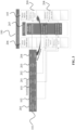
- FIG. 2 shows an example of an "explicit" RDMA Write-with-offset operation (wherein the type of the RDMA operation may be determined or indicated by an opcode 205 in the packet 101), which may be executed by the target device 100 (also referred to as "Physical target host for the RDMA operation") and initiated by the initiator device 110, respectively.
- the packet 101 is shown as provided by the initiator device 110 (not shown).
- the target device 100 can execute the RDMA Write-with-offset operation in the memory 105.
- the memory 105 is comprised by the target device 100.
- the target device 100 also comprises a virtual memory 206, and a NIC 207.
- the RDMA operation is referred to as "explicit", because the one or more offset values 104 to be used in this RDMA operation are indicated (explicitly) by the packet 101.
- the packet 101 includes the first destination address 102 and the destination key 103.
- the destination key 103 is a memory key of the memory 105
- the first destination address 102 is a destination VA.
- the destination VA 102 is an address of the virtual memory 206 and is associated with a buffer of the target device 100.
- the packet 101 further comprises a first offset address 201 and an offset key 202.
- the first offset address 201 is an offset VA.
- the offset VA 201 is an address of the virtual memory 206 and is associated with a location of storage of the offset value 104.
- the offset VA 201 may indicate a physical location 208 of the offset value 104 in the memory 105 of the target device 100 (or alternatively on a remote memory of a further device that the target device 100 is configured to communicate with (alternative not shown)).
- the packet 101 may further comprise data 204 (to be written). The packet 101 would not comprise such data 204 if the RDMA operation was a RDMA Read-with-offset operation.
- the packet 101 may further comprise a data length 203 of the data 204.
- the packet 101 may further comprise the opcode 205, which determines or indicates the RDMA operation to be executed.
- the data 204 may particularly be written by the target device 100 to a physical location 209 in the memory 105 (e.g., a physical location 209 in a certain memory region of the memory 105, wherein the memory region may be indicated by the memory key 103).
- the physical location 209 corresponds to the second destination address 106 (in the example of FIG. 2 , the second destination address 106 is a destination physical address (PA) of the memory 105), which may be derived by the target device 100 based on the destination VA 102 - as provided by the initiator device 110 - and further based on the offset value 104. That is, the data 204 may be written to the destination PA 106.
- PA destination physical address
- the data 204 may thereby be first written using the destination VA 102 of the virtual memory 206, i.e. into the buffer of the target device 100, and then by the target device 100 into the memory 105 using the destination PA 106, i.e., to the physical location 209.
- both sides i.e. the initiator device 110 and the target device 100
- both sides can contribute to generating the second destination address 106.
- the target device 100 is allowed to control the write destination, and thus the operation nature is changed from one-sided (control only at the initiator device 110) to two-sided (control at both devices).
- the destination PA 106 of the memory 105 may be obtained by the target device 100 by translating the destination VA 102 into the destination PA 106 based on a base VA, a base PA of the memory 105, and based on the one or more offset values 104.
- the offset PA identifies the physical location 208 in the memory 105, at which the offset value 104 is stored, and from which it can be obtained by the NIC 207.
- the data length 204 is added to the current offset value 104, and the thus obtained new offset value 104 is stored in the physical location 208 in the memory 105.
- the offset value(s) 104 could also be selected by the initiator device 110 (particularly for the "explicit" RDMA Write-with-offset operation shown in FIG. 2 ), or the offset value(s) 104 may be chosen by the target device 100, for instance, upon arrival of the packet 101. However, the offset value(s) 104 may be located on the target device 100, and may affect the calculation of the second destination address 106 in either way.
- the offset value(s) 104 may generally be modified after any RDMA operation, e.g. the offset value(s) 104 may be increased or decreased. As already mentioned above, the offset value(s) 104 may be increased by the size of the incoming data 204 (included in the packet 101, e.g., as indicated by the data length 203), so that a subsequent, identical RDMA Write-with-offset operation (same destination address 102 given in the packet 101, e.g. same destination VA 102) would not overwrite the previously written data 204, but the new data 204 would rather be written right after the previously written data 204 in the memory 105 at a different physical location.
- a subsequent, identical RDMA Write-with-offset operation (same destination address 102 given in the packet 101, e.g. same destination VA 102) would not overwrite the previously written data 204, but the new data 204 would rather be written right after the previously written data 204 in the memory 105 at a different physical location.
- Destination PA Destination VA ⁇ Base VA + Base PA + Offset Value if the offset value 104 changes (e.g., is increased by the target device 100), the same destination VA 102 in the next packet 101 will result in a different destination PA 106, i.e. a different physical location 208 in the memory 105 to which the data 204 is written.
- the further data 204 may be logically appended to the previously written data 204, when an identical further packet 101 arrives, i.e., the further data 204 included in that identical further packet 101 may be placed right after the previously written data 204 of the previous packet 101, as is shown in FIG. 3 .
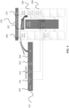
- FIG. 3 shows an example of an RDMA Write-with-offset operation (see opcode 205), in which the destination VA 102 has a value of 0x2111, the memory key 103 has a value of 0x1, the destination VA 102 has a value of 0x3010, the memory key 202 has a value of 0x3, the data length has a value of 0x5, and the data 204 is "ABCDE".
- the base VA has a value of 0x2000
- the base PA has a value of 0x0
- the offset base VA has a value of 0x3000
- the offset base PA has a value of 0x2000.
- the given values are hexadecimal values, wherein 0x denotes the hexadecimal value.
- the offset VA 201 refers to the virtual memory 206 of the target device 100, and the NIC 207 translates the offset VA 201 into the offset PA.
- the offset value 104 that can be obtained from the physical location 208 of the memory 105 corresponding to the offset PA has exemplarily a value of 0x123 in FIG. 3 .
- the data "ABCDE” is then written by the target device 100, particularly the NIC 207, into the physical location 209 in the memory 105 corresponding to the destination PA 106.
- the data 204 may first be written to the buffer of the target device 100 using the destination VA 102, and then from the buffer to the physical location 209 using the destination PA 106.
- the data 204 of the further packet 101 will not overwrite the previously written data 204, since the (new) offset value 104 is now different, namely has now a value of 0x128 and not anymore of 0x123.
- the data 204 of the further packet 101 will thus be logically appended to the previously written data 204.
- the changes (compared to conventional systems and a conventional RDMA Write operation) to the packet 101 and calculation of the second destination address 106, which are described above for the RDMA Write-with-offset operation, can also be applied to the other RDMA operation types. That is, the initiator device 110 and target device 100 may also perform a RDMA Read-with-offset operation, and/or a RDMA Atomic-with-offset operation (not shown in the figures).
- FIG. 4 shows an alternative example to the "explicit" RDMA Write-with-offset operation shown as example in FIG. 2 and FIG. 3 .
- FIG. 4 shows an "implicit" RDMA Write-with-offset operation.
- the operation is referred to as "implicit”, because the one or more offset values 104 are not indicated by the packet 101, but are implicitly derived by the target device 100.
- same elements in FIG. 2 and FIG. 4 share the same reference signs and function likewise.
- the packet 101 remains unchanged compared to the packet 601 of the conventional RDMA Write operation, as shown in FIG. 6 . That is, the packet 101 includes the opcode 205, the destination VA 102, the memory key 103, the data 204 and the data length 203. However, the packet 101 does not include the destination offset VA 201 and the offset key 202 as the packet 101 shown in FIG. 2 .
- the target device 100 nevertheless uses the offset value 104 when translating the destination VA 102 to the destination PA 106 (in the same manner as described with respect to FIG. 2 ).
- the offset value 104 may be controlled by the target device 100 as described for the "explicit" RDMA Write-with-offset operation of FIG. 2 .
- the offset value 104 may, as in the previous "explicit" variant shown in FIG. 2 , be stored at the target device 100, e.g., in the memory 105, in particular the physical location 208.
- the target device 100 obtains the offset value 104 on its own motion, without being given any information in this respect via the packet 101.
- the RDMA operations with offset may further be based on the following principles:
- each packet 101 resp. data 204 is passed only once (a) from the region of the initiator device 110 to its NIC (zero-copy send) and (b) from the NIC 207 of the target device 100 to the destination region (zero-copy receive). This significantly reduces the communication latency.
- FIG. 5 shows a method 500 for executing an RDMA operation according to an embodiment of the invention.
- the method 500 can be performed by the target device 100.
- the method 500 comprises: a step 501 of receiving a packet 101 including a first destination address 102 and a destination key 103; a step 502 of obtaining one or more offset values 104; a step 503 of obtaining a second destination address 106 based on the first destination address 102 and the one or more offset values 104; and a step 504 of initiating the RDMA operation in the memory 105 based on the second destination address 106.
Landscapes
- Engineering & Computer Science (AREA)
- Theoretical Computer Science (AREA)
- Physics & Mathematics (AREA)
- Computer Hardware Design (AREA)
- General Engineering & Computer Science (AREA)
- General Physics & Mathematics (AREA)
- Mathematical Physics (AREA)
- Software Systems (AREA)
- Computer Networks & Wireless Communication (AREA)
- Signal Processing (AREA)
- Bus Control (AREA)
- Memory System Of A Hierarchy Structure (AREA)
Claims (14)
- Vorrichtung (100) zum Ausführen eines direkten Fernspeicherzugriff-Vorgangs, RDMA-Vorgangs, in einem Speicher (105), wobei die Vorrichtung (100) zu Folgendem konfiguriert ist:Empfangen eines Pakets (101), das eine erste Zieladresse (102), einen Zielschlüssel (103), eine oder mehrere erste Offset-Adressen (201) und einen oder mehrere Offset-Schlüssel (202) beinhaltet, wobei die erste Zieladresse eine virtuelle Adresse eines virtuellen Speichers der Vorrichtung ist;Erlangen eines oder mehrerer Offset-Werte (104) basierend auf der einen oder den mehreren ersten Offset-Adressen (201) und dem einen oder den mehreren Offset-Schlüsseln (202);Erlangen einer zweiten Zieladresse (106) basierend auf der ersten Zieladresse (102), dem Zielschlüssel (103) und dem einen oder den mehreren Offset-Werten (104); undInitiieren des RDMA-Vorgangs in dem Speicher (105) basierend auf der zweiten Zieladresse (106).
- Vorrichtung (100) nach Anspruch 1, die ferner zu Folgendem konfiguriert ist:
Initiieren einer Modifikation von mindestens einem Offset-Wert (104), nachdem der RDMA-Vorgang in dem Speicher (105) ausgeführt wurde. - Vorrichtung (100) nach Anspruch 2, wobei:
die Modifikation des mindestens einen Offset-Wertes (104) eine Erhöhung oder eine Verringerung des mindestens einen Offset-Wertes (104) umfasst. - Vorrichtung (100) nach Anspruch 2 oder 3, wobei:das Paket (101) ferner eine Datenlänge (203) umfasst; unddie Vorrichtung (100) ferner dazu konfiguriert ist, die Modifikation des mindestens einen Offset-Wertes (104) basierend auf der Datenlänge (203) zu initiieren.
- Vorrichtung (100) nach einem der Ansprüche 1 bis 4, wobei:die erste Zieladresse (102) eine virtuelle Adresse eines virtuellen Speichers (206) der Vorrichtung (100) ist und die zweite Zieladresse (106) eine physische Adresse des Speichers (105) ist; unddie Vorrichtung (100) ferner dazu konfiguriert ist, die erste Zieladresse (102) basierend auf einer virtuellen Basisadresse, einer physischen Basisadresse des Speichers (105) und dem einen oder den mehreren Offset-Werten (104) in die zweite Zieladresse (106) zu übersetzen.
- Vorrichtung (100) nach einem der Ansprüche 1 bis 5, die ferner zu Folgendem konfiguriert ist:Erlangen einer oder mehrerer zweiter Offset-Adressen basierend auf der einen oder den mehreren ersten Offset-Adressen (201); undErlangen des einen oder der mehreren Offset-Werte (104) unter Verwendung der einen oder der mehreren zweiten Offset-Adressen.
- Vorrichtung (100) nach Anspruch 6, wobei:die eine oder die mehreren ersten Offset-Adressen (201) virtuelle Adressen eines virtuellen Speichers (206) der Vorrichtung (100) sind und die eine oder die mehreren zweiten Offset-Adressen physische Adressen des Speichers (105) sind; unddie Vorrichtung (100) ferner dazu konfiguriert ist, die eine oder die mehreren ersten Offset-Adressen (201) basierend auf einer oder mehreren virtuellen Offset-Basisadressen und einer physischen Offset-Basisadresse des Speichers (105) in die eine oder die mehreren zweiten Offset-Adressen zu übersetzen.
- Vorrichtung (100) nach Anspruch 7, die ferner zu Folgendem konfiguriert ist:
Erlangen der einen oder der mehreren virtuellen Offset-Basisadressen und der physischen Offset-Basisadresse basierend auf dem einen oder den mehreren Offset-Schlüsseln (202). - Vorrichtung (100) nach einem der Ansprüche 1 bis 8, die ferner zu Folgendem konfiguriert ist:Speichern des einen oder der mehreren Offset-Werte (104) in der Vorrichtung (100); und/oderSpeichern des einen oder der mehreren Offset-Werte (104) in dem Speicher (105),wobei die Vorrichtung (100) den Speicher (105) umfasst oder der Speicher (105) ein Fernspeicher ist, zum Kommunizieren mit dem die Vorrichtung (100) konfiguriert ist.
- Vorrichtung (110) zum Initiieren eines direkten Fernspeicherzugriff-Vorgangs, RDMA-Vorgangs, in einem Fernspeicher (105), wobei die Vorrichtung (110) zu Folgendem konfiguriert ist:Bereitstellen eines Pakets (101), das eine Zieladresse (102), einen Zielschlüssel (103), eine oder mehrere Offset-Adressen (201) und einen oder mehrere Offset-Schlüssel (202) beinhaltet, an eine andere Vorrichtung (100),wobei die Zieladresse (102) einen Ort für den RDMA-Vorgang in dem Fernspeicher (105) angibt und die Zieladresse eine virtuelle Adresse eines virtuellen Speichers der anderen Vorrichtung ist undwobei die eine oder die mehreren Offset-Adressen (201) einen Ort eines oder mehrerer Offset-Werte (104) an der anderen Vorrichtung (100) oder in dem Fernspeicher (105) angeben.
- Vorrichtung (100, 110) nach einem der Ansprüche 1 bis 10, wobei:
der RDMA-Vorgang ein RDMA-Schreibvorgang, ein RDMA-Lesevorgang oder ein atomarer RDMA-Vorgang ist. - Verfahren (500) zum Ausführen eines direkten Fernspeicherzugriff-Vorgangs, RDMA-Vorgangs, in einem Speicher (105), wobei das Verfahren (500) Folgendes umfasst:Empfangen (501) eines Pakets (101), das eine erste Zieladresse (102), einen Zielschlüssel (103), eine oder mehrere erste Offset-Adressen (201) und einen oder mehrere Offset-Schlüssel (202) beinhaltet, wobei die erste Zieladresse eine virtuelle Adresse eines virtuellen Speichers der Vorrichtung ist;Erlangen (502) eines oder mehrerer Offset-Werte (104) basierend auf der einen oder den mehreren ersten Offset-Adressen (201) und dem einen oder den mehreren Offset-Schlüsseln (202);Erlangen (503) einer zweiten Zieladresse (106) basierend auf der ersten Zieladresse (102 ) und dem einen oder den mehreren Offset-Werten (104); undInitiieren (504) des RDMA-Vorgangs in dem Speicher (105) basierend auf der zweiten Zieladresse (106).
- Verfahren zum Initiieren eines direkten Fernspeicherzugriff-Vorgangs, RDMA-Vorgangs, in einem Fernspeicher (105), wobei das Verfahren Folgendes umfasst:Bereitstellen eines Pakets (101), das eine Zieladresse (102), einen Zielschlüssel (103), eine oder mehrere Offset-Adressen (201) und einen oder mehrere Offset-Schlüssel (202) beinhaltet,wobei die Zieladresse (102) einen Ort für den RDMA-Vorgang in dem Fernspeicher (105) angibt und die Zieladresse eine virtuelle Adresse eines virtuellen Speichers der anderen Vorrichtung ist undwobei die eine oder die mehreren Offset-Adressen (201) einen Ort eines oder mehrerer Offset-Werte (104) an einer Vorrichtung (100), die den einen oder die mehreren Offset-Werte (104) aufrechterhält, oder in dem Fernspeicher (105) angeben.
- Computerprogramm, umfassend einen Programmcode zum Durchführen des Verfahrens (500) nach Anspruch 12 oder 13, wenn es auf einem Computer ausgeführt wird.
Applications Claiming Priority (1)
| Application Number | Priority Date | Filing Date | Title |
|---|---|---|---|
| PCT/EP2020/062877 WO2021223880A1 (en) | 2020-05-08 | 2020-05-08 | Remote direct memory access with offset values |
Publications (2)
| Publication Number | Publication Date |
|---|---|
| EP4127940A1 EP4127940A1 (de) | 2023-02-08 |
| EP4127940B1 true EP4127940B1 (de) | 2024-10-09 |
Family
ID=70740579
Family Applications (1)
| Application Number | Title | Priority Date | Filing Date |
|---|---|---|---|
| EP20726319.5A Active EP4127940B1 (de) | 2020-05-08 | 2020-05-08 | Direkter fernspeicherzugriff mit offsetwerten |
Country Status (4)
| Country | Link |
|---|---|
| US (1) | US11949740B2 (de) |
| EP (1) | EP4127940B1 (de) |
| CN (1) | CN113939811B (de) |
| WO (1) | WO2021223880A1 (de) |
Families Citing this family (4)
| Publication number | Priority date | Publication date | Assignee | Title |
|---|---|---|---|---|
| EP4127940B1 (de) * | 2020-05-08 | 2024-10-09 | Huawei Technologies Co., Ltd. | Direkter fernspeicherzugriff mit offsetwerten |
| US12242413B2 (en) * | 2021-08-27 | 2025-03-04 | Keysight Technologies, Inc. | Methods, systems and computer readable media for improving remote direct memory access performance |
| CN115017089B (zh) * | 2022-06-01 | 2025-01-28 | 中国科学院计算技术研究所 | 一种远程内存访问的系统及方法 |
| US20260067360A1 (en) * | 2024-09-03 | 2026-03-05 | Hewlett Packard Enterprise Development Lp | Efficient one-sided communication in a distributed system |
Family Cites Families (39)
| Publication number | Priority date | Publication date | Assignee | Title |
|---|---|---|---|---|
| US7813369B2 (en) * | 2004-08-30 | 2010-10-12 | International Business Machines Corporation | Half RDMA and half FIFO operations |
| US20060136697A1 (en) * | 2004-12-16 | 2006-06-22 | Tsao Gary Y | Method, system, and program for updating a cached data structure table |
| US7370174B2 (en) * | 2005-01-05 | 2008-05-06 | Intel Corporation | Method, system, and program for addressing pages of memory by an I/O device |
| US20060236063A1 (en) * | 2005-03-30 | 2006-10-19 | Neteffect, Inc. | RDMA enabled I/O adapter performing efficient memory management |
| US7702826B2 (en) * | 2005-12-28 | 2010-04-20 | Intel Corporation | Method and apparatus by utilizing platform support for direct memory access remapping by remote DMA (“RDMA”)-capable devices |
| US7836274B2 (en) * | 2006-09-05 | 2010-11-16 | Broadcom Corporation | Method and system for combining page buffer list entries to optimize caching of translated addresses |
| US7587575B2 (en) * | 2006-10-17 | 2009-09-08 | International Business Machines Corporation | Communicating with a memory registration enabled adapter using cached address translations |
| US8090790B2 (en) * | 2007-05-30 | 2012-01-03 | Broadcom Corporation | Method and system for splicing remote direct memory access (RDMA) transactions in an RDMA-aware system |
| US8195912B2 (en) * | 2007-12-06 | 2012-06-05 | Fusion-io, Inc | Apparatus, system, and method for efficient mapping of virtual and physical addresses |
| US8108538B2 (en) * | 2008-08-21 | 2012-01-31 | Voltaire Ltd. | Device, system, and method of distributing messages |
| US8655974B2 (en) | 2010-04-30 | 2014-02-18 | International Business Machines Corporation | Zero copy data transmission in a software based RDMA network stack |
| US8468551B2 (en) * | 2010-06-30 | 2013-06-18 | International Business Machines Corporation | Hypervisor-based data transfer |
| US10223326B2 (en) * | 2013-07-31 | 2019-03-05 | Oracle International Corporation | Direct access persistent memory shared storage |
| US9306916B2 (en) * | 2013-12-25 | 2016-04-05 | Cavium, Inc. | System and a method for a remote direct memory access over converged ethernet |
| WO2015118865A1 (ja) * | 2014-02-05 | 2015-08-13 | 日本電気株式会社 | 情報処理装置、情報処理システム及びデータアクセス方法 |
| US9742855B2 (en) | 2014-09-04 | 2017-08-22 | Mellanox Technologies, Ltd. | Hybrid tag matching |
| US20170155717A1 (en) * | 2015-11-30 | 2017-06-01 | Intel Corporation | Direct memory access for endpoint devices |
| WO2017113960A1 (zh) * | 2015-12-28 | 2017-07-06 | 华为技术有限公司 | 一种数据处理方法以及NVMe存储器 |
| US10642780B2 (en) | 2016-03-07 | 2020-05-05 | Mellanox Technologies, Ltd. | Atomic access to object pool over RDMA transport network |
| CN107003816B (zh) * | 2016-06-14 | 2020-06-26 | 华为技术有限公司 | 数据访问方法和相关装置及系统 |
| US20180188974A1 (en) * | 2016-12-30 | 2018-07-05 | Intel Corporation | Computer program product, system, and method to allow a host and a storage device to communicate using different fabric, transport, and direct memory access protocols |
| US10769081B2 (en) * | 2016-12-30 | 2020-09-08 | Intel Corporation | Computer program product, system, and method to allow a host and a storage device to communicate between different fabrics |
| US10803039B2 (en) * | 2017-05-26 | 2020-10-13 | Oracle International Corporation | Method for efficient primary key based queries using atomic RDMA reads on cache friendly in-memory hash index |
| US10353826B2 (en) * | 2017-07-14 | 2019-07-16 | Arm Limited | Method and apparatus for fast context cloning in a data processing system |
| US10509728B2 (en) * | 2017-09-29 | 2019-12-17 | Intel Corporation | Techniques to perform memory indirection for memory architectures |
| US20190102287A1 (en) * | 2017-09-29 | 2019-04-04 | Intel Corporation | Remote persistent memory access device |
| US10496595B2 (en) * | 2017-12-14 | 2019-12-03 | Mellanox Technologies, Ltd. | Method for zero-copy object serialization and deserialization |
| CN115941616B (zh) * | 2017-12-15 | 2025-02-25 | 微软技术许可有限责任公司 | 多路径rdma传输 |
| CN110392084B (zh) * | 2018-04-20 | 2022-02-15 | 伊姆西Ip控股有限责任公司 | 在分布式系统中管理地址的方法、设备和计算机程序产品 |
| JP7075067B2 (ja) * | 2018-06-22 | 2022-05-25 | 日本電気株式会社 | ストレージ装置 |
| US10977193B2 (en) * | 2018-08-17 | 2021-04-13 | Oracle International Corporation | Remote direct memory operations (RDMOs) for transactional processing systems |
| US10296451B1 (en) * | 2018-11-01 | 2019-05-21 | EMC IP Holding Company LLC | Content addressable storage system utilizing content-based and address-based mappings |
| CN113287286B (zh) * | 2019-01-30 | 2022-12-27 | 华为技术有限公司 | 通过rdma进行分布式存储节点中的输入/输出处理 |
| CN113366457B (zh) * | 2019-01-31 | 2024-06-14 | 国际商业机器公司 | 处理输入/输出存储指令 |
| US12327138B2 (en) * | 2019-10-16 | 2025-06-10 | EMC IP Holding Company LLC | Storage system with efficient release of address lock waiters during synchronous replication |
| EP4127940B1 (de) * | 2020-05-08 | 2024-10-09 | Huawei Technologies Co., Ltd. | Direkter fernspeicherzugriff mit offsetwerten |
| CN114026548A (zh) * | 2020-05-28 | 2022-02-08 | 华为技术有限公司 | 直接内存访问的方法和系统 |
| WO2021239230A1 (en) * | 2020-05-28 | 2021-12-02 | Huawei Technologies Co., Ltd. | Method and system for direct memory access |
| US12487824B2 (en) * | 2021-09-21 | 2025-12-02 | Intel Corporation | Immediate offset of load store and atomic instructions |
-
2020
- 2020-05-08 EP EP20726319.5A patent/EP4127940B1/de active Active
- 2020-05-08 CN CN202080018268.1A patent/CN113939811B/zh active Active
- 2020-05-08 WO PCT/EP2020/062877 patent/WO2021223880A1/en not_active Ceased
-
2022
- 2022-11-08 US US17/983,146 patent/US11949740B2/en active Active
Also Published As
| Publication number | Publication date |
|---|---|
| EP4127940A1 (de) | 2023-02-08 |
| US11949740B2 (en) | 2024-04-02 |
| CN113939811B (zh) | 2025-09-19 |
| US20230061873A1 (en) | 2023-03-02 |
| CN113939811A (zh) | 2022-01-14 |
| WO2021223880A1 (en) | 2021-11-11 |
Similar Documents
| Publication | Publication Date | Title |
|---|---|---|
| US11949740B2 (en) | Remote direct memory access with offset values | |
| US10908961B2 (en) | RDMA (remote direct memory access) data transfer in a virtual environment | |
| US10911358B1 (en) | Packet processing cache | |
| US7587575B2 (en) | Communicating with a memory registration enabled adapter using cached address translations | |
| TWI239187B (en) | System and method for managing and validating remote keys which correspond to outstanding data transactions | |
| US20070041383A1 (en) | Third party node initiated remote direct memory access | |
| JP3391315B2 (ja) | バス制御装置 | |
| HUP0302879A2 (hu) | Eljárás és berendezés adatfolyam vezérléséhez adatfeldolgozó rendszerek között memórián keresztül | |
| JPH10504665A (ja) | バスブリッジにおけるトランザクション順序を維持し、遅延応答をサポートする方法及びそのための装置 | |
| US10963295B2 (en) | Hardware accelerated data processing operations for storage data | |
| JP7671732B2 (ja) | ホストコンピューティングデバイスおよびネットワークインターフェースデバイスを備えるプログラマブルネットワークインターフェースデバイス | |
| EP4324181B1 (de) | Netzwerkschnittstellenkarte zum cachen von dateisystem-internen strukturen | |
| US10802828B1 (en) | Instruction memory | |
| US10042554B2 (en) | Increased bandwidth of ordered stores in a non-uniform memory subsystem | |
| CN103649921A (zh) | 促进通信环境的隔离存储空间之间的通信 | |
| US6766358B1 (en) | Exchanging messages between computer systems communicatively coupled in a computer system network | |
| CN114924794B (zh) | 一种存储部件的发射队列的地址存储、调度方法和装置 | |
| CN115859334A (zh) | 一种加解密数据处理方法及装置 | |
| US20140012904A1 (en) | Providing byte enables for peer-to-peer data transfer within a computing environment | |
| US20250252067A1 (en) | Remote node control using rdma | |
| CN118633075A (zh) | 一种处理请求的方法、装置及系统 | |
| HK1193890A (en) | Method, apparatus and computer system for facilitating communication in a communication environment | |
| HK1193890B (en) | Method, apparatus and computer system for facilitating communication in a communication environment |
Legal Events
| Date | Code | Title | Description |
|---|---|---|---|
| STAA | Information on the status of an ep patent application or granted ep patent |
Free format text: STATUS: UNKNOWN |
|
| STAA | Information on the status of an ep patent application or granted ep patent |
Free format text: STATUS: THE INTERNATIONAL PUBLICATION HAS BEEN MADE |
|
| PUAI | Public reference made under article 153(3) epc to a published international application that has entered the european phase |
Free format text: ORIGINAL CODE: 0009012 |
|
| STAA | Information on the status of an ep patent application or granted ep patent |
Free format text: STATUS: REQUEST FOR EXAMINATION WAS MADE |
|
| 17P | Request for examination filed |
Effective date: 20221026 |
|
| AK | Designated contracting states |
Kind code of ref document: A1 Designated state(s): AL AT BE BG CH CY CZ DE DK EE ES FI FR GB GR HR HU IE IS IT LI LT LU LV MC MK MT NL NO PL PT RO RS SE SI SK SM TR |
|
| DAV | Request for validation of the european patent (deleted) | ||
| DAX | Request for extension of the european patent (deleted) | ||
| GRAP | Despatch of communication of intention to grant a patent |
Free format text: ORIGINAL CODE: EPIDOSNIGR1 |
|
| STAA | Information on the status of an ep patent application or granted ep patent |
Free format text: STATUS: GRANT OF PATENT IS INTENDED |
|
| INTG | Intention to grant announced |
Effective date: 20240503 |
|
| GRAS | Grant fee paid |
Free format text: ORIGINAL CODE: EPIDOSNIGR3 |
|
| GRAA | (expected) grant |
Free format text: ORIGINAL CODE: 0009210 |
|
| STAA | Information on the status of an ep patent application or granted ep patent |
Free format text: STATUS: THE PATENT HAS BEEN GRANTED |
|
| AK | Designated contracting states |
Kind code of ref document: B1 Designated state(s): AL AT BE BG CH CY CZ DE DK EE ES FI FR GB GR HR HU IE IS IT LI LT LU LV MC MK MT NL NO PL PT RO RS SE SI SK SM TR |
|
| REG | Reference to a national code |
Ref country code: CH Ref legal event code: EP |
|
| REG | Reference to a national code |
Ref country code: DE Ref legal event code: R096 Ref document number: 602020039041 Country of ref document: DE |
|
| REG | Reference to a national code |
Ref country code: IE Ref legal event code: FG4D |
|
| P01 | Opt-out of the competence of the unified patent court (upc) registered |
Free format text: CASE NUMBER: APP_53630/2024 Effective date: 20240926 |
|
| REG | Reference to a national code |
Ref country code: NL Ref legal event code: FP |
|
| REG | Reference to a national code |
Ref country code: LT Ref legal event code: MG9D |
|
| REG | Reference to a national code |
Ref country code: AT Ref legal event code: MK05 Ref document number: 1731333 Country of ref document: AT Kind code of ref document: T Effective date: 20241009 |
|
| PG25 | Lapsed in a contracting state [announced via postgrant information from national office to epo] |
Ref country code: HR Free format text: LAPSE BECAUSE OF FAILURE TO SUBMIT A TRANSLATION OF THE DESCRIPTION OR TO PAY THE FEE WITHIN THE PRESCRIBED TIME-LIMIT Effective date: 20241009 Ref country code: PT Free format text: LAPSE BECAUSE OF FAILURE TO SUBMIT A TRANSLATION OF THE DESCRIPTION OR TO PAY THE FEE WITHIN THE PRESCRIBED TIME-LIMIT Effective date: 20250210 Ref country code: IS Free format text: LAPSE BECAUSE OF FAILURE TO SUBMIT A TRANSLATION OF THE DESCRIPTION OR TO PAY THE FEE WITHIN THE PRESCRIBED TIME-LIMIT Effective date: 20250209 |
|
| PG25 | Lapsed in a contracting state [announced via postgrant information from national office to epo] |
Ref country code: FI Free format text: LAPSE BECAUSE OF FAILURE TO SUBMIT A TRANSLATION OF THE DESCRIPTION OR TO PAY THE FEE WITHIN THE PRESCRIBED TIME-LIMIT Effective date: 20241009 |
|
| PG25 | Lapsed in a contracting state [announced via postgrant information from national office to epo] |
Ref country code: BG Free format text: LAPSE BECAUSE OF FAILURE TO SUBMIT A TRANSLATION OF THE DESCRIPTION OR TO PAY THE FEE WITHIN THE PRESCRIBED TIME-LIMIT Effective date: 20241009 |
|
| PG25 | Lapsed in a contracting state [announced via postgrant information from national office to epo] |
Ref country code: ES Free format text: LAPSE BECAUSE OF FAILURE TO SUBMIT A TRANSLATION OF THE DESCRIPTION OR TO PAY THE FEE WITHIN THE PRESCRIBED TIME-LIMIT Effective date: 20241009 |
|
| PG25 | Lapsed in a contracting state [announced via postgrant information from national office to epo] |
Ref country code: NO Free format text: LAPSE BECAUSE OF FAILURE TO SUBMIT A TRANSLATION OF THE DESCRIPTION OR TO PAY THE FEE WITHIN THE PRESCRIBED TIME-LIMIT Effective date: 20250109 |
|
| PG25 | Lapsed in a contracting state [announced via postgrant information from national office to epo] |
Ref country code: LV Free format text: LAPSE BECAUSE OF FAILURE TO SUBMIT A TRANSLATION OF THE DESCRIPTION OR TO PAY THE FEE WITHIN THE PRESCRIBED TIME-LIMIT Effective date: 20241009 Ref country code: GR Free format text: LAPSE BECAUSE OF FAILURE TO SUBMIT A TRANSLATION OF THE DESCRIPTION OR TO PAY THE FEE WITHIN THE PRESCRIBED TIME-LIMIT Effective date: 20250110 Ref country code: AT Free format text: LAPSE BECAUSE OF FAILURE TO SUBMIT A TRANSLATION OF THE DESCRIPTION OR TO PAY THE FEE WITHIN THE PRESCRIBED TIME-LIMIT Effective date: 20241009 |
|
| PG25 | Lapsed in a contracting state [announced via postgrant information from national office to epo] |
Ref country code: PL Free format text: LAPSE BECAUSE OF FAILURE TO SUBMIT A TRANSLATION OF THE DESCRIPTION OR TO PAY THE FEE WITHIN THE PRESCRIBED TIME-LIMIT Effective date: 20241009 |
|
| PG25 | Lapsed in a contracting state [announced via postgrant information from national office to epo] |
Ref country code: RS Free format text: LAPSE BECAUSE OF FAILURE TO SUBMIT A TRANSLATION OF THE DESCRIPTION OR TO PAY THE FEE WITHIN THE PRESCRIBED TIME-LIMIT Effective date: 20250109 |
|
| PGFP | Annual fee paid to national office [announced via postgrant information from national office to epo] |
Ref country code: NL Payment date: 20250409 Year of fee payment: 6 |
|
| PG25 | Lapsed in a contracting state [announced via postgrant information from national office to epo] |
Ref country code: SM Free format text: LAPSE BECAUSE OF FAILURE TO SUBMIT A TRANSLATION OF THE DESCRIPTION OR TO PAY THE FEE WITHIN THE PRESCRIBED TIME-LIMIT Effective date: 20241009 |
|
| PGFP | Annual fee paid to national office [announced via postgrant information from national office to epo] |
Ref country code: DE Payment date: 20250402 Year of fee payment: 6 |
|
| PG25 | Lapsed in a contracting state [announced via postgrant information from national office to epo] |
Ref country code: DK Free format text: LAPSE BECAUSE OF FAILURE TO SUBMIT A TRANSLATION OF THE DESCRIPTION OR TO PAY THE FEE WITHIN THE PRESCRIBED TIME-LIMIT Effective date: 20241009 |
|
| REG | Reference to a national code |
Ref country code: DE Ref legal event code: R097 Ref document number: 602020039041 Country of ref document: DE |
|
| PG25 | Lapsed in a contracting state [announced via postgrant information from national office to epo] |
Ref country code: EE Free format text: LAPSE BECAUSE OF FAILURE TO SUBMIT A TRANSLATION OF THE DESCRIPTION OR TO PAY THE FEE WITHIN THE PRESCRIBED TIME-LIMIT Effective date: 20241009 |
|
| PG25 | Lapsed in a contracting state [announced via postgrant information from national office to epo] |
Ref country code: RO Free format text: LAPSE BECAUSE OF FAILURE TO SUBMIT A TRANSLATION OF THE DESCRIPTION OR TO PAY THE FEE WITHIN THE PRESCRIBED TIME-LIMIT Effective date: 20241009 |
|
| PG25 | Lapsed in a contracting state [announced via postgrant information from national office to epo] |
Ref country code: SK Free format text: LAPSE BECAUSE OF FAILURE TO SUBMIT A TRANSLATION OF THE DESCRIPTION OR TO PAY THE FEE WITHIN THE PRESCRIBED TIME-LIMIT Effective date: 20241009 |
|
| PG25 | Lapsed in a contracting state [announced via postgrant information from national office to epo] |
Ref country code: CZ Free format text: LAPSE BECAUSE OF FAILURE TO SUBMIT A TRANSLATION OF THE DESCRIPTION OR TO PAY THE FEE WITHIN THE PRESCRIBED TIME-LIMIT Effective date: 20241009 |
|
| PG25 | Lapsed in a contracting state [announced via postgrant information from national office to epo] |
Ref country code: IT Free format text: LAPSE BECAUSE OF FAILURE TO SUBMIT A TRANSLATION OF THE DESCRIPTION OR TO PAY THE FEE WITHIN THE PRESCRIBED TIME-LIMIT Effective date: 20241009 |
|
| PLBE | No opposition filed within time limit |
Free format text: ORIGINAL CODE: 0009261 |
|
| STAA | Information on the status of an ep patent application or granted ep patent |
Free format text: STATUS: NO OPPOSITION FILED WITHIN TIME LIMIT |
|
| PG25 | Lapsed in a contracting state [announced via postgrant information from national office to epo] |
Ref country code: SE Free format text: LAPSE BECAUSE OF FAILURE TO SUBMIT A TRANSLATION OF THE DESCRIPTION OR TO PAY THE FEE WITHIN THE PRESCRIBED TIME-LIMIT Effective date: 20241009 |
|
| 26N | No opposition filed |
Effective date: 20250710 |
|
| REG | Reference to a national code |
Ref country code: CH Ref legal event code: H13 Free format text: ST27 STATUS EVENT CODE: U-0-0-H10-H13 (AS PROVIDED BY THE NATIONAL OFFICE) Effective date: 20251223 |
|
| PG25 | Lapsed in a contracting state [announced via postgrant information from national office to epo] |
Ref country code: LU Free format text: LAPSE BECAUSE OF NON-PAYMENT OF DUE FEES Effective date: 20250508 |
|
| PG25 | Lapsed in a contracting state [announced via postgrant information from national office to epo] |
Ref country code: CH Free format text: LAPSE BECAUSE OF NON-PAYMENT OF DUE FEES Effective date: 20250531 |
|
| REG | Reference to a national code |
Ref country code: BE Ref legal event code: MM Effective date: 20250531 |
|
| PG25 | Lapsed in a contracting state [announced via postgrant information from national office to epo] |
Ref country code: MC Free format text: LAPSE BECAUSE OF FAILURE TO SUBMIT A TRANSLATION OF THE DESCRIPTION OR TO PAY THE FEE WITHIN THE PRESCRIBED TIME-LIMIT Effective date: 20241009 |
|
| PGFP | Annual fee paid to national office [announced via postgrant information from national office to epo] |
Ref country code: GB Payment date: 20260325 Year of fee payment: 7 |
|
| PG25 | Lapsed in a contracting state [announced via postgrant information from national office to epo] |
Ref country code: IE Free format text: LAPSE BECAUSE OF NON-PAYMENT OF DUE FEES Effective date: 20250508 |
|
| PG25 | Lapsed in a contracting state [announced via postgrant information from national office to epo] |
Ref country code: BE Free format text: LAPSE BECAUSE OF NON-PAYMENT OF DUE FEES Effective date: 20250531 |
|
| PG25 | Lapsed in a contracting state [announced via postgrant information from national office to epo] |
Ref country code: FR Free format text: LAPSE BECAUSE OF NON-PAYMENT OF DUE FEES Effective date: 20250531 |