EP4150353B1 - Empfänger für elektromagnetisches feld - Google Patents
Empfänger für elektromagnetisches feld Download PDFInfo
- Publication number
- EP4150353B1 EP4150353B1 EP21731174.5A EP21731174A EP4150353B1 EP 4150353 B1 EP4150353 B1 EP 4150353B1 EP 21731174 A EP21731174 A EP 21731174A EP 4150353 B1 EP4150353 B1 EP 4150353B1
- Authority
- EP
- European Patent Office
- Prior art keywords
- coupling
- variation
- signal
- power
- frequency
- Prior art date
- Legal status (The legal status is an assumption and is not a legal conclusion. Google has not performed a legal analysis and makes no representation as to the accuracy of the status listed.)
- Active
Links
Images


Classifications
-
- H—ELECTRICITY
- H04—ELECTRIC COMMUNICATION TECHNIQUE
- H04B—TRANSMISSION
- H04B10/00—Transmission systems employing electromagnetic waves other than radio-waves, e.g. infrared, visible or ultraviolet light, or employing corpuscular radiation, e.g. quantum communication
- H04B10/07—Arrangements for monitoring or testing transmission systems; Arrangements for fault measurement of transmission systems
- H04B10/073—Arrangements for monitoring or testing transmission systems; Arrangements for fault measurement of transmission systems using an out-of-service signal
-
- H—ELECTRICITY
- H04—ELECTRIC COMMUNICATION TECHNIQUE
- H04B—TRANSMISSION
- H04B10/00—Transmission systems employing electromagnetic waves other than radio-waves, e.g. infrared, visible or ultraviolet light, or employing corpuscular radiation, e.g. quantum communication
-
- H—ELECTRICITY
- H04—ELECTRIC COMMUNICATION TECHNIQUE
- H04B—TRANSMISSION
- H04B1/00—Details of transmission systems, not covered by a single one of groups H04B3/00 - H04B13/00; Details of transmission systems not characterised by the medium used for transmission
- H04B1/38—Transceivers, i.e. devices in which transmitter and receiver form a structural unit and in which at least one part is used for functions of transmitting and receiving
- H04B1/40—Circuits
-
- G—PHYSICS
- G01—MEASURING; TESTING
- G01R—MEASURING ELECTRIC VARIABLES; MEASURING MAGNETIC VARIABLES
- G01R29/00—Arrangements for measuring or indicating electric quantities not covered by groups G01R19/00 - G01R27/00
- G01R29/08—Measuring electromagnetic field characteristics
- G01R29/0864—Measuring electromagnetic field characteristics characterised by constructional or functional features
- G01R29/0878—Sensors; antennas; probes; detectors
- G01R29/0885—Sensors; antennas; probes; detectors using optical probes, e.g. electro-optical, luminescent, glow discharge, or optical interferometers
-
- H—ELECTRICITY
- H04—ELECTRIC COMMUNICATION TECHNIQUE
- H04B—TRANSMISSION
- H04B1/00—Details of transmission systems, not covered by a single one of groups H04B3/00 - H04B13/00; Details of transmission systems not characterised by the medium used for transmission
- H04B1/06—Receivers
- H04B1/16—Circuits
-
- H—ELECTRICITY
- H04—ELECTRIC COMMUNICATION TECHNIQUE
- H04B—TRANSMISSION
- H04B2210/00—Indexing scheme relating to optical transmission systems
- H04B2210/006—Devices for generating or processing an RF signal by optical means
Definitions
- the present invention relates to an electromagnetic field receiver.
- this invention relates to a Radio Frequency (RF) receiver.
- RF Radio Frequency
- RF receivers such as a dipole antenna
- metallic conductors in which electrons move along the conductor in response to an incident RF electric field to produce a small current.
- This current may then be processed (e.g. utilising electronic circuits, mixers, amplifiers and digitisers) to convert this small current into a demodulated, amplified signal.
- a new form of RF receiver is based on a Rydberg atom.
- a Rydberg atom is an atom with one or more electrons excited to a very high principal quantum number. These Rydberg atoms have several useful properties, such as very large dipole moments and long decay periods. These properties can be exploited to create an RF receiver that may receive and demodulate Amplitude-Modulated (AM), Frequency-Modulated (FM) and Phase Modulated (PM) RF electric fields over very large frequency ranges (e.g. from hundreds of MHz to 1 THz).
- AM Amplitude-Modulated
- FM Frequency-Modulated
- PM Phase Modulated
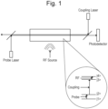
- An example Rydberg-atom based RF receiver is shown in Figure 1 and operates as follows.
- An atomic medium is provided which, in this example, is a glass cell filled with a low density vapour of alkali atoms (such as Rubidium-85).
- Each Rubidium-85 atom has a number of electron states, including the ground state (
- the outer electron of the Rubidium-85 atom may be excited (e.g. by absorbing a photon of a particular wavelength) from the ground state (
- the electron may then decay from the excited state to a lower excited state (that is, an excited state at a lower energy level) or to the ground state (
- a lower excited state that is, an excited state at a lower energy level
- some of these transitions are not allowed as they are dipole forbidden.
- a first laser (known as a "probe” laser) is passed through the atomic medium at a first wavelength which corresponds to the energy required to elevate the Rubidium-85 atom's outer electron from its ground state (
- a second laser (known as a “coupling” laser) is also passed through the atomic medium in an opposing direction at a relatively large power level (compared to the probe laser) and at a second wavelength which corresponds to the energy required to elevate the Rubidium-85 atom's outer electron from the first excited state (
- 1>) is forbidden so that the ground state (
- This phenomenon is known as Electromagnetically Induced Transparency (EIT) and the received signal is known as the EIT signal.
- EIT Electromagnetically Induced Transparency
- the received signal is known as the EIT signal.
- EIT Electromagnetically Induced Transparency
- the received signal is known as the EIT signal.
- the above description is of a ladder scheme EIT effect, but the skilled person would understand that the EIT effect may be realised through alternative electron transitions, such as the Vee and Lambda schemes.
- a Rydberg-atom based FM RF receiver works in a similar manner. That is, when the RF electric field changes (or “detunes") from its resonant RF transition frequency, the EIT signal splits into two non-symmetrical peaks. The separation of the two peaks increases with RF detuning. By locking the probe laser and coupling laser to particular frequencies, then the optical detector output is directly correlated to the FM RF electric field.
- Rydberg RF receivers may also be used to detect phase modulated RF fields, such as those of Binary Phase-Shift Keying (BPSK), Quadrature Phase-Shift Keying (QPSK), and Quadrature Amplitude Modulation (QAM) signals (used in many wireless and cellular communications protocols).
- phase modulated RF fields such as those of Binary Phase-Shift Keying (BPSK), Quadrature Phase-Shift Keying (QPSK), and Quadrature Amplitude Modulation (QAM) signals (used in many wireless and cellular communications protocols).
- BPSK Binary Phase-Shift Keying
- QPSK Quadrature Phase-Shift Keying
- QAM Quadrature Amplitude Modulation
- the Rydberg atom based RF detector may be configured to detect RF fields of a specific frequency by selecting a particular second wavelength of the coupling laser so that the electrons of the atomic medium are elevated to a particular Rydberg state.
- This Rydberg state is selected so that photons at the specific frequency to be detected will elevate electrons from this Rydberg state to its adjacent Rydberg state, thus creating a detectable change in the EIT signal that may be observed at the optical detector.
- the magnitude of the EIT signal known as the "modulation depth" is the difference between the depth of the drop in amplitude of the EIT signal when there is an incident RF electric field and when there is no incident RF electric field.
- the EIT signal is at its optimal depth (i.e. thereby giving an optimal Signal to Noise Ratio (SNR)) when the frequency of the RF field matches (i.e. is "resonant" with) the energy required for the transition from this particular Rydberg state to its adjacent Rydberg state. It is desirable to maximise this depth so as to enable higher speed and/or lower error rate communications. However, as the RF field being detected may drift away from this resonant frequency (e.g. due to Doppler shift or antenna drift), the EIT signal's depth may be sub-optimal. It is desirable to alleviate this problem.
- SNR Signal to Noise Ratio
- European Patent Application No. 3308146 A discloses a method for measuring the electric field of electromagnetic radiation using the spectroscopic responses of Rydberg atoms to the electromagnetic radiation field.
- Fiber-coupled vapor cell for a portable Rydberg atom-based radio frequency electric field sensor MATT T. SIMONS ET AL, APPLIED OPTICS, vol 57, no 22, 26 July 2018 discloses a movable, Rydberg atom-based Radio Frequency (RF) electric (E) field probe.
- RF Radio Frequency
- Chinese Patent Application No. 107179450 A discloses amicrowave electric field strength measurement method and measurement apparatus.
- Chinese Patent Application No. 107462849 A discloses a measurement apparatus and method of the radio frequency line transmission factor based on atomic energy level.
- US Patent No. 6826339 B1 discloses an electromagnetically induced transparent (EIT) photonic band-gap fiber (PBG).
- EIT electromagnetically induced transparent
- PBG photonic band-gap fiber
- the variation in the coupling frequency may cause a greater variation in the change in power of the probe signal at the optical receiver than a variation in the intensity value
- the method may further comprise the steps of: vary the coupling frequency of the coupling signal so as to cause the variation in the change in power of the probe signal at the optical receiver; monitor the variation in the change in power of the probe signal in response to the variation of the coupling frequency; based on the monitoring in response to the variation of the coupling frequency, set the coupling frequency of the coupling signal so as to increase the change in power of the probe signal; and then, vary the intensity value of the coupling signal so as to cause the variation in the change in power of the probe signal at the optical receiver; monitor the variation in the change in power of the probe signal in response to the variation of the intensity value; based on the monitoring in response to the variation of the intensity value, set the intensity value of the coupling signal so as to increase the change in power of the probe signal.
- the variation in the intensity value may cause a greater variation in the change in power of the probe signal at the optical receiver than a variation in the coupling frequency
- the method may further comprise the steps of: vary the intensity value of the coupling signal so as to cause the variation in the change in power of the probe signal at the optical receiver; monitor the variation in the change in power of the probe signal in response to the variation of the intensity value; based on the monitoring in response to the variation of the intensity value, set the intensity value of the coupling signal so as to increase the change in power of the probe signal; and then, vary the coupling frequency of the coupling signal so as to cause the variation in the change in power of the probe signal at the optical receiver; monitor the variation in the change in power of the probe signal in response to the variation of the coupling frequency; based on the monitoring in response to the variation of the coupling frequency, set the coupling frequency of the coupling signal so as to increase the change in power of the probe signal.
- the steps of varying the intensity value and/or coupling frequency of the coupling signal, monitoring the variation in the change in power of the probe signal, and setting the coupling frequency based on the monitoring may be performed iteratively until a termination condition is met.
- the termination condition may be that the power of the probe signal following the change is less than or equal to the power of the probe signal before the change.
- the transmission medium may include a metal vapour, which may be an alkali metal, which may be one of: Rubidium, Caesium or Strontium.
- the electromagnetic field may be a Radio Frequency, RF, field and the electromagnetic field detector may be an RF detector.
- a computer program product comprising instructions which, when the program is executed by a computer, cause the computer to carry out the method of the first aspect of the invention.
- the computer program may be stored on a computer-readable data carrier.
- the wireless telecommunications network 1 includes a wireless transmitter 10 and a Radio-Frequency (RF) receiver 20.
- the wireless transmitter 10 is configured to transmit wireless signals at a frequency of 3.5GHz and at a transmission power of 1mW, and the wireless transmitter 10 and RF receiver 20 are 250km apart.
- the RF receiver 20 is a Rydberg-atom based RF receiver and includes an optical fibre 21, a probe laser 23, a coupling laser 25 and a photodetector 27.
- the RF receiver 20 also includes a processor 29 for processing the received signal data of the photodetector 27.
- the optical fibre 21 includes an optical cavity containing a vapour of alkali metal (in this embodiment, Rubidium-85).
- the RF receiver 20 is configured to detect the 3.5GHz wireless signals transmitted by the wireless transmitter 10.
- the probe laser 23 of the RF receiver 20 transmits a probe signal along the optical fibre 21, through the optical cavity of Rubidium-85 vapour.
- the coupling laser 25 of the RF receiver 20 transmits a coupling signal along the optical fibre 21, through the optical cavity of Rubidium-85 vapour.
- the frequency of the probe signal is set to correlate with the transition of an electron of a Rubidium-85 atom from a ground state to a first excited state
- the frequency of the coupling signal is set to correlate with the transition of an electron of a Rubidium-85 atom from the first excited state to a predetermined Rydberg state.
- the RF receiver 20 is configured to detect 3.5GHz wireless signals, which is the 84 th principal quantum number energy state.
- wireless signals transmitted by the wireless transmitter at 3.5GHz that pass through the optical cavity of the optical fibre 21 will excite electrons from this predetermined Rydberg state to an adjacent Rydberg state, causing an Electromagnetically Induced Transparency (EIT) signal in the monitored probe signal at the photodetector 27.
- EIT Electromagnetically Induced Transparency
- a difference between a depth of the EIT signal when there is an incident wireless signal from the wireless transmitter 10 and where there is no incident wireless signal from the wireless transmitter 10 is the "modulation depth".
- the RF receiver 20 also has a controller 22 for controlling a frequency of the probe signal (i.e. to adjust or stabilise the frequency of the probe signal), for controlling a frequency of the coupling signal (i.e. to adjust or stabilise the frequency of the coupling signal), for controlling an intensity of the probe laser 23 (i.e. the transmission power and/or cross-sectional area of the probe laser 23), and for controlling an intensity of the coupling laser 25 (i.e. the transmission power and/or cross-sectional area of the coupling laser 25).
- the controller 22 also includes a processor module and a memory module, wherein the memory module is configured to store values for various measurements of the RF receiver 20 (described below) and the processor module is configured to analyse these measurements (also described below).
- the controller 22 utilises a Pound-Drever-Hall (PDH) stabilising mechanism for stabilising the frequencies of the probe and coupling signals, and utilises an Acousto-Optic Modulator (AOM) stabilising mechanism for stabilising the intensity of the probe and coupling lasers 23, 25.
- PDH Pound-Drever-Hall
- AOM Acousto-Optic Modulator
- This first embodiment adjusts certain parameters of the coupling laser to improve the modulation depth (that is, increase the modulation depth relative to the modulation depth if no action is taken) in response to the frequency of the wireless transmitter 10 signals deviating from 3.5GHz and/or the transmission power of the wireless transmitter 10 being reduced from 1mW.
- a deviation between a target frequency and a frequency of the transmitted signal is known as "detuning", and in this particular instance when it applies to the wireless transmitter's signal deviating from the target frequency, it is known as "RF detuning”. This RF detuning may occur due to, for example, frequency drift in the antenna and Doppler shift.
- this RF detuning can lead to a reduction in the modulation depth at the photodetector, which is undesirable. Furthermore, any reduction in the transmission power of the wireless transmitter 10 also leads to a reduction in the modulation depth at the photodetector. This reduction may occur due to, for example, free-space loss or multi-path interference.
- this embodiment proposes a solution by adjusting parameters of the coupling laser so as to maximise (or at least improve) the modulation depth without knowing the RF detuning of the signal transmitted by the wireless transmitter 10 or a change in transmission power of the wireless transmitter 10.
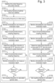
- step S101 the controller 22 stabilises the frequency of the probe signal (which is configured for exciting electrons of the Rubidium-85 atom from the ground state to the first excited state) and the intensity of the probe laser 23.
- step S103 the intensity of the coupling laser 25 is set at the optimum value for the transition of electrons from the first excited state to the predetermined (that is, 84 th principal quantum number) Rydberg state, and the stabilised at this intensity.
- the optimal intensity of the coupling laser 25 may be determined by combining ⁇ c 2 with the beam width of coupling laser 25 and the relevant dipole moment for the transition from the first excited state to the predetermined Rydberg state so that it is equal to ⁇ 2 ⁇ 3 .
- This value may also be determined experimentally (e.g. in an initial calibration step) by setting the probe, coupling and RF frequencies to resonance, then for high powers of RF measuring the value of coupling power at which the modulation depth is maximum, then iteratively reducing the RF power and measuring the optimum coupling power.
- the RF receiver is configured to detect 3.5GHz wireless signals transmitted by the wireless transmitter 10.
- the photodetector 29 experiences a drop in amplitude of the probe signals (compared to the probe signal amplitude when there is no wireless signal incident on the RF receiver 20), wherein the drop in amplitude is known as the "modulation depth").
- the processor 29, monitoring the signal of the photodetector 27, measures the modulation depth and records both the value of the coupling detuning at the time of this measurement and the value of the measured modulation depth in memory.
- a "detuning" is a deviation between a reference frequency and a frequency of the transmitted signal.
- the reference frequency is that required to transition electrons from the first exited state to the predetermined Rydberg state (assuming zero RF detuning).
- the "coupling detuning" is the deviation between the reference frequency of the coupling signal (set in step S105) and the actual frequency of the signal transmitted by the coupling laser 25.
- the recorded value for the coupling detuning is zero.
- this causes a change in the modulation depth of the probe signal, which can be used as feedback to adjust the frequency of the coupling signal to compensate for any RF detuning and/or changes in transmission power of the wireless signal of the wireless transmitter 10 (that is, to maximise or at least increase the modulation depth, which would otherwise decrease as a result of the RF detuning and/or changes in transmission power).
- step S111 the processor 29 measures the modulation depth with the new frequency of the coupling signal (that is, the frequency of the coupling signal following the adjustment at step S109).
- the value of the coupling detuning at the time of the measurement (+100Hz) and the value of the modulation depth are recorded in memory.
- step S113 the controller's processor module analyses the values recorded in steps S105 and S111 (those recorded when the coupling detuning was zero and +100Hz respectively) to characterise a change in modulation depth following the increment of 100Hz. If the modulation depth increased as a result of this increment, then it is determined that there is an RF detuning of the wireless signal and/or reduction in transmission power of the wireless transmitter 10 and that the adjustment to increment the coupling detuning compensated for that RF detuning and/or reduction in transmission power. The controller 22 may react to such a result of this analysis by further incrementing the coupling detuning (as described in subsequent steps of this method).
- the controller 22 may react to such a result of this analysis by decrementing the coupling detuning (as described in subsequent steps of this method). Accordingly, this analysis determines the direction for coupling signal frequency adjustments (being either the first direction to increment the frequency or a second direction to decrement the frequency) that result in a modulation depth increase.
- step S115 the controller 22 adjusts the frequency of the coupling signal based on the results of the analysis in step S113. That is, if the modulation depth increased as a result of the previous adjustment, then the controller 22 adjusts the frequency by the predetermined adjustment amount in the first direction (that is, a further increment); and if the modulation depth decreased as a result of the previous adjustment, then the controller 22 adjusts the frequency by the predetermined adjustment amount in the second direction (i.e. a decrement of -100Hz).
- the processor 29 measures the new modulation depth and records the value of the coupling detuning and the measured modulation depth value.
- Steps S115 and S117 are repeated in an iterative manner until a termination condition is met in which the modulation depth does not increase (i.e. no change or a decrease in modulation depth) following the frequency adjustment.
- a termination condition is met in which the modulation depth does not increase (i.e. no change or a decrease in modulation depth) following the frequency adjustment.
- an optimal frequency for the coupling signal is calculated by interpolating the recorded values of the coupling detuning and the corresponding measured modulation depth values and the controller 22 sets the value of the frequency of the coupling signal at this calculated optimal value.
- the coupling signal is thereafter stabilised at this calculated optimal value by the controller 22.
- step S123 the processor 29 measures the modulation depth with the frequency of the coupling signal being the calculated optimal value and with the intensity being that calculated in step S103. These values are recorded in memory.
- step S125 the controller 22 adjusts the intensity of the coupling laser 25 (from the value set in step S103 above) by a particular adjustment amount (1dB) in a first direction (in this embodiment, an increment so that the intensity of the coupling laser 25 is the value determined in step S103 plus 1 dB).
- step S127 the processor 29 measures the modulation depth with the new intensity of the coupling laser 25.
- the value of the intensity of the coupling laser 25 at the time of the measurement (+1dB) and the value of the modulation depth are recorded in memory.
- step S129 the controller's processor module analyses the values recorded in steps S123 and S127 (those recorded when the intensity was at the value calculated in step 103 and +1dB respectively) to characterise a change in modulation depth following the increment of +1dB. If the modulation depth increased as a result of this increment, then it is determined that there is an RF detuning of the wireless signal and/or reduction in transmission power of the wireless transmitter 10 and that the adjustment to increment the intensity of the coupling laser 25 compensated for that RF detuning and/or reduction in transmission power. The controller 22 may react to such a result of this analysis by further incrementing the intensity of the coupling laser 25 (as described in subsequent steps of this method).
- the controller 22 may react to such a result of this analysis by decrementing the intensity of the coupling laser 25 (as described in subsequent steps of this method). Accordingly, this analysis determines the direction for coupling laser intensity adjustments (being either the first direction to increment the intensity or a second direction to decrement the intensity) that result in a modulation depth increase.
- step S131 the controller 22 adjusts the intensity of the coupling laser 25 based on the results of the analysis in step S129. That is, if the modulation depth increased as a result of the previous adjustment, then the controller 22 adjusts the intensity by the predetermined adjustment amount in the first direction (that is, a further increment); and if the modulation depth decreased as a result of the previous adjustment, then the controller 22 adjusts the intensity by the predetermined adjustment amount in the second direction (i.e. a decrement of -1dB). Following this new adjustment, in step S133, the controller 22 measures the new modulation depth and records the value of the intensity of the coupling laser 25 and the measured modulation depth value.
- Steps S131 and S133 are repeated in an iterative manner until a termination condition is met in which the modulation depth does not increase (i.e. no change or a decrease in modulation depth) following the intensity adjustment. Then, in step S135, an optimal intensity for the coupling laser 25 is calculated by interpolating the recorded values of the intensity of the coupling laser 25 and the corresponding measured modulation depth values and the controller 22 sets the value of the intensity of the coupling laser 25 at this calculated optimal value. The coupling laser 25 is thereafter stabilised at this calculated optimal value by the controller 22.
- the process then loops back to step S107 to track any further changes in RF detuning and/or transmission power of the wireless transmitter 10 and maximise (or at least increase) the modulation depth in response.
- the process may also loop back to step S103 should the RF receiver 20 be reconfigured to detect wireless signals at different frequencies.
- the above embodiment provides a process of introducing feedback loops into the RF receiver 20 so that the modulation depth may be maximised or at least increased.
- These feedback loops include a first feedback loop based on a relationship between the modulation depth and the coupling detuning, and a second feedback loop based on a relationship between the modulation depth and the intensity of the coupling laser 25. It is preferable to perform the first feedback loop before the second feedback loop, as there is a stronger relationship between the modulation depth and the coupling detuning than between the modulation depth and the intensity of the coupling laser 25 (that is, there are greater changes in the modulation depth as a result of the frequency adjustment than the intensity adjustment).
- the present inventors have derived the electric susceptibility, X, for a low-density atomic vapour with the ladder EIT configuration as:
- the absorbance determines the proportion of the incident probe intensity that is transmitted through a length L of the optical cavity containing the Rubidium-85 vapour (specifically, the region within the optical cavity where the probe and coupling lasers overlap): Probe transmission ⁇ exp ⁇ I X 2 ⁇ L / ⁇ p where ⁇ p is the probe wavelength.
- On-Off Keying represents digital data with the presence or absence of the RF signal.
- the presence of the RF signal for a specific duration represents a binary one, while its absence for the same duration represents a binary zero.
- the modulation depth of the probe signal will be the difference in the transmitted optical intensity detected by the photodetector 27 when the RF signal is on and when it is off. It is assumed here that the modulation rate of the RF signal is sufficiently slow to allow the EIT effect to reach a steady state between each bit of data transmission.
- the EIT effect is small and the value of the absorbance is also small, so to a good approximation the modulation depth is simply proportional to the difference in the absorbance when the RF intensity is at its maximum and when it is zero: M ⁇ I X ⁇ r ⁇ I X 0
- the total absorbance is the sum of the off-resonant absorbances for the adjacent RF transitions.
- the coupling detuning should be incremented (or decremented) in the direction of increasing modulation depth until the gradient falls to zero or becomes negative.
- the position of the maximum can be interpolated given the coupling detuning and modulation depth values on either side of it. Now at this point the coupling detuning has been optimised for a non-optimum choice of coupling intensity.
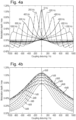
- the two points to notice from the curves in Figure 4b are that:
- the modulation depth is most sensitive to the coupling detuning, with only a weak dependence on the coupling intensity (that is, unless the adjustment size for the coupling intensity is relatively fine compared to the adjustment size for the coupling frequency so that coupling intensity changes cause greater changes in modulation depth).
- the following description is a numerical example for a system having a wireless transmitter 10 transmitting a wireless signal at 30 ⁇ V/m.
- Figure 5a is graph illustrating how resonant RF frequency varies with principal quantum number n
- Figure 5b is a graph illustrating how resonant RF frequency varies with coupling frequency.
- the optical coupling frequency is so much larger than the RF frequency, the proportional change in coupling frequency between resonances is just -0.002% whereas the proportional change in the RF frequency is -4%.
- FWHM Full-Width-Half-Maximum
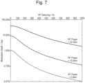
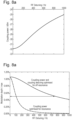
- FIG. 8a shows how the optimum coupling power varies as a function of the RF detuning for the special case of low RF power and balanced coupling/RF detunings, as described by Equation 5. It can be seen that the optimum coupling power needs to be increased as the RF signal moves away from resonance.
- Figure 8b shows the improvement that can be achieved by using this increased coupling power with RF detuning compared to simply using the resonant value.
- Optimising both coupling power and coupling detuning for off-resonant RF signal increases FWHM from 196 Hz to 1420 Hz for this special case of a very weak RF signal (1mW from 250km distance).
- a receiver that is tunable across a FWHM of 1420 Hz can track the Doppler-shifted 3.5GHz signal of a vehicle's transmitter moving radially from 0 m/s up to 122m/s (270 mph), so this is a useful tuning range even at this extremely low RF transmit power.
- the modulation depth when receiving an off-resonant RF signal, can be optimised by varying both coupling frequency and coupling power, but the modulation depth will not be as large as it is on-resonance and the tuning range is ultimately limited by the RF transmit power and the minimum detectable modulation depth.
- the above embodiment illustrates an example system for detecting wireless signals of 3.5GHz and a method to optimise the modulation depth of the Rydberg-atom based RF detector.
- the above method may be applied to many other electromagnetic signals of different frequencies, and the 3.5GHz signal is just an example. That is, for a particular target frequency, a system may be configured such that an EIT signal is produced on a probe signal by an incident electromagnetic signal at that target frequency (such as by selecting an appropriate atomic medium (e.g. Rubidium, Caesium or Strontium) having Rydberg states that correspond with that target frequency).
- an appropriate atomic medium e.g. Rubidium, Caesium or Strontium
- the values of the other physical quantities resonant frequencies, transition rates, dipole moments
- the EIT signal is produced following a ladder configuration of electron transitions. That is, any configuration (e.g. Lambda, Vee) may be used.
- a first feedback loop based on the relationship between modulation depth and coupling detuning was used first (to adjust the coupling frequency) before using a second feedback loop based on the relationship between modulation depth and intensity of the coupling laser (to adjust the intensity of the coupling laser).
- a second feedback loop based on the relationship between modulation depth and intensity of the coupling laser to adjust the intensity of the coupling laser.
- step S105 the system is reset to the initial state, and then the intensity is adjusted by its smallest adjustment value from the initial state and the modulation depth is recorded. It may then be determined whether the coupling frequency or the intensity of the coupling laser should be adjusted in the first feedback loop based on whether the coupling frequency adjustment or the intensity adjustment caused the greatest change in modulation depth.
Landscapes
- Engineering & Computer Science (AREA)
- Computer Networks & Wireless Communication (AREA)
- Signal Processing (AREA)
- Physics & Mathematics (AREA)
- Electromagnetism (AREA)
- General Physics & Mathematics (AREA)
- Optical Communication System (AREA)
- Magnetic Resonance Imaging Apparatus (AREA)
Claims (13)
- Verfahren zum Steuern eines Elektromagnetfelddetektors (20), wobei der Elektromagnetfelddetektor (20) einen ersten und zweiten optischen Sender (23, 25), ein Übertragungsmedium (21) und einen optischen Empfänger (27) umfasst, wobei der erste optische Sender (23) dazu ausgelegt ist, ein Sondensignal über das Übertragungsmedium (21) mit einer Sondenfrequenz zu dem optischen Empfänger (27) zu übertragen, und der zweite Sender (25) dazu ausgelegt ist, ein Kopplungssignal über das Übertragungsmedium (21) mit einer Kopplungsfrequenz zu übertragen, wobei die Sondenfrequenz so eingestellt ist, dass Elektronen des Übertragungsmediums (21) von einem Grundzustand in einen ersten angeregten Zustand angeregt werden, und die Kopplungsfrequenz so eingestellt ist, dass Elektronen des Übertragungsmediums (21) in einen vorbestimmten angeregten Zustand angeregt werden, um einen Effekt der elektromagnetisch induzierten Transparenz (EIT) in dem Elektromagnetfelddetektor (20) zu induzieren, sodass ein einfallendes elektromagnetisches Feld am Übertragungsmedium (21) eine detektierbare Änderung der Leistung des Sondensignals am optischen Empfänger (27) bewirkt, wobei das Verfahren die folgenden Schritte umfasst:Variieren eines oder beides von einem Intensitätswert und der Kopplungsfrequenz des Kopplungssignals, um eine Variation in der Änderung der Leistung des Sondensignals am optischen Empfänger (27) aufgrund des einfallenden elektromagnetischen Feldes am Übertragungsmedium (21) zu bewirken;Überwachen der Variation in der Änderung der Leistung des Sondensignals aufgrund des einfallenden elektromagnetischen Feldes am Übertragungsmedium (21); undbasierend auf dem Überwachen, Einstellen des Intensitätswerts und/oder der Kopplungsfrequenz des Kopplungssignals, um die Änderung der Leistung des Sondensignals zu erhöhen.
- Verfahren nach Anspruch 1, wobei eine Variation in der Kopplungsfrequenz eine größere Variation in der Änderung der Leistung des Sondensignals am optischen Empfänger (27) bewirkt als eine Variation im Intensitätswert, und das Verfahren die folgenden Schritte umfasst:Variieren der Kopplungsfrequenz des Kopplungssignals, um die Variation in der Änderung der Leistung des Sondensignals am optischen Empfänger (27) aufgrund des einfallenden elektromagnetischen Feldes am Übertragungsmedium (21) zu bewirken;Überwachen der Variation in der Änderung der Leistung des Sondensignals aufgrund des einfallenden elektromagnetischen Feldes am Übertragungsmedium (21) als Reaktion auf die Variation der Kopplungsfrequenz;basierend auf dem Überwachen als Reaktion auf die Variation der Kopplungsfrequenz, Einstellen der Kopplungsfrequenz des Kopplungssignals, um die Änderung der Leistung des Sondensignals zu erhöhen; und dann Variieren des Intensitätswerts des Kopplungssignals, um die Variation in der Änderung der Leistung des Sondensignals am optischen Empfänger (27) aufgrund des einfallenden elektromagnetischen Feldes am Übertragungsmedium (21) zu bewirken;Überwachen der Variation in der Änderung der Leistung des Sondensignals aufgrund des einfallenden elektromagnetischen Feldes am Übertragungsmedium (27) als Reaktion auf die Variation des Intensitätswerts;basierend auf dem Überwachen als Reaktion auf die Variation des Intensitätswerts, Einstellen des Intensitätswerts des Kopplungssignals, um die Änderung der Leistung des Sondensignals zu erhöhen.
- Verfahren nach Anspruch 1, wobei eine Variation im Intensitätswert eine größere Variation in der Änderung der Leistung des Sondensignals am optischen Empfänger (27) bewirkt als eine Variation in der Kopplungsfrequenz, und das Verfahren die folgenden Schritte umfasst:Variieren des Intensitätswerts des Kopplungssignals, um die Variation in der Änderung der Leistung des Sondensignals am optischen Empfänger (27) aufgrund des einfallenden elektromagnetischen Feldes am Übertragungsmedium (21) zu bewirken;Überwachen der Variation in der Änderung der Leistung des Sondensignals aufgrund des einfallenden elektromagnetischen Feldes am Übertragungsmedium (21) als Reaktion auf die Variation des Intensitätswerts;basierend auf dem Überwachen als Reaktion auf die Variation des Intensitätswerts, Einstellen des Intensitätswerts des Kopplungssignals, um die Änderung der Leistung des Sondensignals zu erhöhen; und dann Variieren der Kopplungsfrequenz des Kopplungssignals, um die Variation in der Änderung der Leistung des Sondensignals am optischen Empfänger (27) aufgrund des einfallenden elektromagnetischen Feldes am Übertragungsmedium (21) zu bewirken;Überwachen der Variation in der Änderung der Leistung des Sondensignals aufgrund des einfallenden elektromagnetischen Feldes am Übertragungsmedium (21) als Reaktion auf die Variation der Kopplungsfrequenz;basierend auf dem Überwachen als Reaktion auf die Variation der Kopplungsfrequenz, Einstellen der Kopplungsfrequenz des Kopplungssignals, um die Änderung der Leistung des Sondensignals zu erhöhen.
- Verfahren nach einem der vorstehenden Ansprüche, wobei die Schritte des Variierens des Intensitätswerts und/oder der Kopplungsfrequenz des Kopplungssignals, des Überwachens der Variation in der Änderung der Leistung des Sondensignals und des Einstellens der Kopplungsfrequenz basierend auf dem Überwachen iterativ durchgeführt werden, bis eine Beendigungsbedingung erfüllt ist.
- Verfahren nach Anspruch 4, wobei die Beendigungsbedingung lautet, dass die Leistung des Sondensignals im Anschluss an die Änderung kleiner oder gleich der Leistung des Sondensignals vor der Änderung ist.
- Verfahren nach einem der vorstehenden Ansprüche, wobei das Übertragungsmedium (21) einen Metalldampf beinhaltet.
- Verfahren nach Anspruch 6, wobei der Metalldampf von einem Alkalimetall ist.
- Verfahren nach Anspruch 7, wobei der Alkalimetalldampf eines von Folgendem ist: Rubidium, Caesium oder Strontium.
- Verfahren nach einem der vorstehenden Ansprüche, wobei das elektromagnetische Feld ein Hochfrequenzfeld, HF-Feld, ist und der Elektromagnetfelddetektor (20) ein HF-Detektor ist.
- Elektromagnetfelddetektorsteuerung (22) mit einem Prozessor, der dazu ausgelegt ist, die Schritte nach einem der Ansprüche 1 bis 9 zu implementieren.
- System, das einen Elektromagnetfelddetektor (20) und die Elektromagnetfelddetektorsteuerung (22) nach Anspruch 10 umfasst.
- Computerprogrammprodukt, das Anweisungen umfasst, um zu bewirken, dass die Elektromagnetfelddetektorsteuerung (22) nach Anspruch 10 das Verfahren nach einem der Ansprüche 1 bis 9 ausführt.
- Computerlesbarer Datenträger, auf dem das Computerprogramm nach Anspruch 12 gespeichert ist.
Applications Claiming Priority (2)
| Application Number | Priority Date | Filing Date | Title |
|---|---|---|---|
| GB2010995.5A GB2597260B (en) | 2020-07-16 | 2020-07-16 | Electromagnetic field receiver |
| PCT/EP2021/065655 WO2022017679A1 (en) | 2020-07-16 | 2021-06-10 | Electromagnetic field receiver |
Publications (2)
| Publication Number | Publication Date |
|---|---|
| EP4150353A1 EP4150353A1 (de) | 2023-03-22 |
| EP4150353B1 true EP4150353B1 (de) | 2023-09-06 |
Family
ID=72338894
Family Applications (1)
| Application Number | Title | Priority Date | Filing Date |
|---|---|---|---|
| EP21731174.5A Active EP4150353B1 (de) | 2020-07-16 | 2021-06-10 | Empfänger für elektromagnetisches feld |
Country Status (5)
| Country | Link |
|---|---|
| US (1) | US12267103B2 (de) |
| EP (1) | EP4150353B1 (de) |
| CN (1) | CN115803663B (de) |
| GB (1) | GB2597260B (de) |
| WO (1) | WO2022017679A1 (de) |
Families Citing this family (9)
| Publication number | Priority date | Publication date | Assignee | Title |
|---|---|---|---|---|
| CN114424111B (zh) | 2019-10-24 | 2022-12-27 | 英国电讯有限公司 | 传播信号的设备和系统以及电磁场检测器及操作其的方法 |
| GB2597260B (en) | 2020-07-16 | 2022-12-07 | British Telecomm | Electromagnetic field receiver |
| GB2605123B (en) | 2021-03-01 | 2023-04-26 | British Telecomm | Electromagnetic field detector |
| GB2605651A (en) * | 2021-04-09 | 2022-10-12 | British Telecomm | Electromagnetic field receiver |
| GB2605650B (en) | 2021-04-09 | 2023-06-07 | British Telecomm | Electromagnetic field detector |
| GB2606167B (en) | 2021-04-27 | 2023-06-21 | British Telecomm | Wireless transceiver |
| EP4277166A1 (de) * | 2022-05-13 | 2023-11-15 | British Telecommunications public limited company | Detektor für elektromagnetische felder |
| EP4569338B1 (de) | 2022-08-10 | 2026-02-18 | British Telecommunications Public Limited Company | Detektor für elektromagnetische felder |
| WO2025061378A1 (en) * | 2023-09-22 | 2025-03-27 | British Telecommunications Public Limited Company | A device for a wireless telecommunications network, a system comprising the device, and a method of operating the device |
Family Cites Families (53)
| Publication number | Priority date | Publication date | Assignee | Title |
|---|---|---|---|---|
| US5892582A (en) | 1996-10-18 | 1999-04-06 | Micron Optics, Inc. | Fabry Perot/fiber Bragg grating multi-wavelength reference |
| US6489609B1 (en) * | 1999-05-21 | 2002-12-03 | Hitachi, Ltd. | Ion trap mass spectrometry and apparatus |
| SG120880A1 (en) * | 2001-08-31 | 2006-04-26 | Semiconductor Energy Lab | Laser irradiation method, laser irradiation apparatus, and method of manufacturing a semiconductor device |
| WO2003034113A2 (en) | 2001-10-19 | 2003-04-24 | Nkt Research & Innovation A/S | Integrated photonic crystal structure and method of producing same |
| US6826339B1 (en) * | 2003-11-14 | 2004-11-30 | Corning Incorporated | Electromagnetically induced transparent (EIT) photonic band-gap fibers |
| JP2009519473A (ja) | 2005-10-17 | 2009-05-14 | コーニンクレッカ フィリップス エレクトロニクス エヌ ヴィ | 集積puf |
| ATE426968T1 (de) | 2005-11-29 | 2009-04-15 | Koninkl Philips Electronics Nv | Physisches verteilen von geheimnissen und beweisen der nahe unter verwendung von pufs |
| US8005332B2 (en) * | 2007-05-09 | 2011-08-23 | The Regents Of The University Of California | Integrated optical vapor cell apparatus for precision spectroscopy |
| US8054073B2 (en) * | 2008-05-21 | 2011-11-08 | Entanglement Technologies, Llc | Method and apparatus for implementing EIT magnetometry |
| EP2230794A3 (de) | 2009-03-16 | 2011-10-05 | Technische Universität München | Auf dem Weg zu elektrischen, integrierten Implementierungen von SIMPL Systemen |
| JP2011089868A (ja) | 2009-10-22 | 2011-05-06 | Seiko Epson Corp | ファイバーセル、磁気センサー、及び磁界測定装置 |
| DE102010030358B4 (de) | 2010-06-22 | 2014-05-22 | Osram Opto Semiconductors Gmbh | Verfahren zum Abtrennen einer Substratscheibe |
| US10451694B2 (en) * | 2014-02-24 | 2019-10-22 | Northrop Grumman Systems Corporation | Probe beam frequency stabilization in an atomic sensor system |
| US9651504B2 (en) | 2014-07-30 | 2017-05-16 | B.G. Negev Technologies And Applications Ltd., At Ben-Gurion University | Fano resonance microwave spectroscopy of high absorption matter |
| US10705799B2 (en) | 2015-03-04 | 2020-07-07 | Carol Y. Scarlett | Transmission of information through the use of quantum-optical effects within a multi-layered birefringent structure |
| CN104714110B (zh) | 2015-04-02 | 2017-09-26 | 山西大学 | 基于电磁诱导透明效应测量高频微波场强的装置和方法 |
| EP3308146B1 (de) * | 2015-06-15 | 2020-02-26 | The Regents of The University of Michigan | Atombasierter sensor zur messung des elektrischen feldes von elektromagnetischer strahlung |
| JP6722867B2 (ja) * | 2016-03-09 | 2020-07-15 | パナソニックIpマネジメント株式会社 | 光検出装置および光検出システム |
| WO2017177105A1 (en) | 2016-04-07 | 2017-10-12 | The Johns Hopkins University | System and method for physical one-way function authentication via chaotic integrated photonic resonators |
| CN205691490U (zh) | 2016-06-21 | 2016-11-16 | 中国计量大学 | 一种基于游标效应的级联型fpi氢气传感器 |
| CN106124856B (zh) | 2016-07-25 | 2018-10-26 | 山西大学 | 直接溯源至原子高激发态间跃迁频率的射频源校准方法 |
| US10547460B2 (en) | 2016-11-18 | 2020-01-28 | Qualcomm Incorporated | Message-based key generation using physical unclonable function (PUF) |
| JP6898448B2 (ja) | 2016-12-09 | 2021-07-07 | テレフオンアクチーボラゲット エルエム エリクソン(パブル) | 分散マッシブmimoのための改良されたアンテナ装置 |
| CN108152602B (zh) | 2016-12-15 | 2021-11-26 | 中国计量科学研究院 | 一种基于量子相干效应的天线增益测量装置 |
| CN107179450B (zh) * | 2017-05-31 | 2019-10-11 | 华南师范大学 | 一种微波电场强度测量方法和测量装置 |
| CN107462849B (zh) * | 2017-07-21 | 2020-01-03 | 山西大学 | 一种基于原子能级的射频线传输因子的测量装置及方法 |
| GR20170100352A (el) | 2017-07-26 | 2019-04-04 | Eulambia Advanced Technologies Μον. Επε | Οπτικη φυσικη μη κλωνοποιησιμη συναρτηση βασισμενη σε πολυτροπο οπτικο κυματοδηγο |
| EP4542237A3 (de) * | 2017-12-18 | 2025-06-25 | Rydberg Technologies Inc. | Messelement für atombasiertes elektromagnetisches feld und messsystem |
| CN108809341B (zh) * | 2018-05-25 | 2020-04-17 | 山西大学 | 一种基于里德堡原子的量子天线调频波接收装置和方法 |
| US10684591B1 (en) * | 2018-06-27 | 2020-06-16 | The Government Of The United States Of America As Represent By The Secretary Of The Air Force | Optical rubidium atomic frequency standard |
| CN108927314B (zh) | 2018-07-25 | 2020-06-30 | 哈尔滨工业大学(深圳) | 一种基于无芯光纤的分布式光纤激光超声换能装置 |
| CN109040067B (zh) | 2018-08-02 | 2020-12-11 | 广东工业大学 | 一种基于物理不可克隆技术puf的用户认证设备及认证方法 |
| CN109142891A (zh) | 2018-09-25 | 2019-01-04 | 北京理工大学 | 基于里德堡原子量子相干效应的天线近场测试探头及方法 |
| CN109342830B (zh) | 2018-10-23 | 2021-07-02 | 山西大学 | 全光纤马赫曾德尔干涉仪的微波场强原子测量装置 |
| US11194094B2 (en) | 2018-11-05 | 2021-12-07 | Case Western Reserve University | Multilayered structures and uses thereof in security markings |
| US11218316B2 (en) | 2018-12-05 | 2022-01-04 | Ares Technologies, Inc. | Secure computing hardware apparatus |
| US10979147B2 (en) * | 2019-03-11 | 2021-04-13 | Government Of The United States Of America, As Represented By The Secretary Of Commerce | Rydberg atom mixer and determining phase of modulated carrier radiation |
| CN109905177A (zh) | 2019-03-13 | 2019-06-18 | 华南师范大学 | 基于微波光波相干转换的无线数字通信接收天线及其方法 |
| US10763966B1 (en) * | 2019-03-25 | 2020-09-01 | Otago Innovation Limited | Data communications system using an optical antenna |
| CN114424111B (zh) * | 2019-10-24 | 2022-12-27 | 英国电讯有限公司 | 传播信号的设备和系统以及电磁场检测器及操作其的方法 |
| GB2588754B (en) | 2019-10-24 | 2022-05-11 | British Telecomm | Wireless telecommunications network |
| US12470411B2 (en) | 2020-01-20 | 2025-11-11 | Universiteit Twente (Ut) | Time-domain physical unclonable key (TPUK) authenticated communication |
| US11165505B2 (en) | 2020-02-12 | 2021-11-02 | Government Of The United States Of America, As Represented By The Secretary Of Commerce | Quantum atomic receiving antenna and quantum sensing of radiofrequency radiation |
| US11592469B2 (en) | 2020-05-29 | 2023-02-28 | Rydberg Technologies Inc. | Atom-based closed-loop control for electromagnetic radiation measurement, communications, and information processing |
| US12352568B2 (en) | 2020-06-23 | 2025-07-08 | Clemson University Research Foundation | Physical unclonable function from an integrated photonic interferometer |
| GB2597260B (en) | 2020-07-16 | 2022-12-07 | British Telecomm | Electromagnetic field receiver |
| GB2599400A (en) | 2020-09-30 | 2022-04-06 | Nchain Holdings Ltd | Physically unclonable functions |
| GB202017392D0 (en) | 2020-11-03 | 2020-12-16 | British Telecomm | Physical unclonable functions |
| GB2605123B (en) | 2021-03-01 | 2023-04-26 | British Telecomm | Electromagnetic field detector |
| CN113514698B (zh) | 2021-03-01 | 2024-05-17 | 中国科学院大学 | 一种测量微波相位的装置和方法 |
| GB2606167B (en) | 2021-04-27 | 2023-06-21 | British Telecomm | Wireless transceiver |
| CN113504415B (zh) | 2021-06-01 | 2023-07-21 | 中国科学院大学 | 一种里德堡原子微波鉴相器系统及其相位测量方法 |
| US11402479B1 (en) | 2022-02-08 | 2022-08-02 | Quantum Valley Ideas Laboratories | Communicating information using photonic crystal transceivers |
-
2020
- 2020-07-16 GB GB2010995.5A patent/GB2597260B/en active Active
-
2021
- 2021-06-10 CN CN202180049005.1A patent/CN115803663B/zh active Active
- 2021-06-10 EP EP21731174.5A patent/EP4150353B1/de active Active
- 2021-06-10 WO PCT/EP2021/065655 patent/WO2022017679A1/en not_active Ceased
- 2021-06-10 US US18/005,318 patent/US12267103B2/en active Active
Also Published As
| Publication number | Publication date |
|---|---|
| EP4150353A1 (de) | 2023-03-22 |
| CN115803663B (zh) | 2023-07-07 |
| GB2597260A (en) | 2022-01-26 |
| US12267103B2 (en) | 2025-04-01 |
| CN115803663A (zh) | 2023-03-14 |
| US20230261743A1 (en) | 2023-08-17 |
| GB2597260B (en) | 2022-12-07 |
| WO2022017679A1 (en) | 2022-01-27 |
| GB202010995D0 (en) | 2020-09-02 |
Similar Documents
| Publication | Publication Date | Title |
|---|---|---|
| EP4150353B1 (de) | Empfänger für elektromagnetisches feld | |
| Yamamoto et al. | Coherent optical fiber transmission systems | |
| Yao et al. | Multiloop optoelectronic oscillator | |
| US20240204876A1 (en) | Wireless transceiver | |
| EP4302104B1 (de) | Detektor für elektromagnetisches feld | |
| Yang et al. | Wideband Rydberg atom-based receiver for amplitude modulation radio frequency communication | |
| Marsan et al. | Shadowing variability in an urban land mobile environment at 900 MHz | |
| Wyatt et al. | 1.52 μm PSK heterodyne experiment featuring an external cavity diode laser local oscillator | |
| Chen et al. | Harnessing Rydberg atomic receivers: From quantum physics to wireless communications | |
| Zhang et al. | Tunable off-resonant Rydberg microwave frequency comb spectroscopy based on metawaveguide coupled Rydberg atoms | |
| Stohr et al. | Integrated 460 GHz photonic transmitter module | |
| US12411162B2 (en) | Electromagnetic field detector | |
| EP1883805B1 (de) | Terahertz-detektor | |
| KR20230137241A (ko) | 원자 기반의 전기장 검출 시스템 | |
| Lei et al. | Satellite Signal Detection via Rydberg-Atom Receiver | |
| Du | Terahertz essential devices technique research based on quantum communication | |
| Morohashi et al. | Photonics Generation of THz Signals at 4.7 THz Using a Modulator-Based Optical Comb Source | |
| Cherniak et al. | On the Tunability of Mode Locked Laser Diodes for Use as Local Oscillators in Photonic Terahertz Systems | |
| Li et al. | Millimeter-Wave Optoelectronic Mixing Detector Based on InGaAs Nano-air-channel Photodiode | |
| Tzeremes et al. | Wireless communication with smart photonic antennas using transmission power control | |
| CN120415580A (zh) | 基于原子天线的远距离光载射频传输系统及方法 | |
| Novak et al. | Locking range of a hybrid mode-locked monolithic DBR semiconductor laser at millimeter-wave frequencies | |
| Cai et al. | Sensitivity improvement of Rydberg atom-based microwave sensing via electromagnetically induced transparency | |
| Acedo et al. | 64-Mb/s data transmission beyond the relaxation oscillation frequency using monolithically integrated two laterally coupled diode lasers | |
| Logan | Fiber-optic delay-line stabilization of heterodyne optical signal generator and method using same |
Legal Events
| Date | Code | Title | Description |
|---|---|---|---|
| STAA | Information on the status of an ep patent application or granted ep patent |
Free format text: STATUS: UNKNOWN |
|
| STAA | Information on the status of an ep patent application or granted ep patent |
Free format text: STATUS: THE INTERNATIONAL PUBLICATION HAS BEEN MADE |
|
| PUAI | Public reference made under article 153(3) epc to a published international application that has entered the european phase |
Free format text: ORIGINAL CODE: 0009012 |
|
| STAA | Information on the status of an ep patent application or granted ep patent |
Free format text: STATUS: REQUEST FOR EXAMINATION WAS MADE |
|
| 17P | Request for examination filed |
Effective date: 20221216 |
|
| AK | Designated contracting states |
Kind code of ref document: A1 Designated state(s): AL AT BE BG CH CY CZ DE DK EE ES FI FR GB GR HR HU IE IS IT LI LT LU LV MC MK MT NL NO PL PT RO RS SE SI SK SM TR |
|
| GRAP | Despatch of communication of intention to grant a patent |
Free format text: ORIGINAL CODE: EPIDOSNIGR1 |
|
| STAA | Information on the status of an ep patent application or granted ep patent |
Free format text: STATUS: GRANT OF PATENT IS INTENDED |
|
| INTG | Intention to grant announced |
Effective date: 20230330 |
|
| GRAS | Grant fee paid |
Free format text: ORIGINAL CODE: EPIDOSNIGR3 |
|
| P01 | Opt-out of the competence of the unified patent court (upc) registered |
Effective date: 20230623 |
|
| GRAA | (expected) grant |
Free format text: ORIGINAL CODE: 0009210 |
|
| STAA | Information on the status of an ep patent application or granted ep patent |
Free format text: STATUS: THE PATENT HAS BEEN GRANTED |
|
| AK | Designated contracting states |
Kind code of ref document: B1 Designated state(s): AL AT BE BG CH CY CZ DE DK EE ES FI FR GB GR HR HU IE IS IT LI LT LU LV MC MK MT NL NO PL PT RO RS SE SI SK SM TR |
|
| DAV | Request for validation of the european patent (deleted) | ||
| DAX | Request for extension of the european patent (deleted) | ||
| REG | Reference to a national code |
Ref country code: GB Ref legal event code: FG4D |
|
| REG | Reference to a national code |
Ref country code: CH Ref legal event code: EP |
|
| REG | Reference to a national code |
Ref country code: DE Ref legal event code: R096 Ref document number: 602021004988 Country of ref document: DE |
|
| REG | Reference to a national code |
Ref country code: IE Ref legal event code: FG4D |
|
| REG | Reference to a national code |
Ref country code: LT Ref legal event code: MG9D |
|
| REG | Reference to a national code |
Ref country code: NL Ref legal event code: MP Effective date: 20230906 |
|
| PG25 | Lapsed in a contracting state [announced via postgrant information from national office to epo] |
Ref country code: GR Free format text: LAPSE BECAUSE OF FAILURE TO SUBMIT A TRANSLATION OF THE DESCRIPTION OR TO PAY THE FEE WITHIN THE PRESCRIBED TIME-LIMIT Effective date: 20231207 |
|
| PG25 | Lapsed in a contracting state [announced via postgrant information from national office to epo] |
Ref country code: SE Free format text: LAPSE BECAUSE OF FAILURE TO SUBMIT A TRANSLATION OF THE DESCRIPTION OR TO PAY THE FEE WITHIN THE PRESCRIBED TIME-LIMIT Effective date: 20230906 Ref country code: RS Free format text: LAPSE BECAUSE OF FAILURE TO SUBMIT A TRANSLATION OF THE DESCRIPTION OR TO PAY THE FEE WITHIN THE PRESCRIBED TIME-LIMIT Effective date: 20230906 Ref country code: NO Free format text: LAPSE BECAUSE OF FAILURE TO SUBMIT A TRANSLATION OF THE DESCRIPTION OR TO PAY THE FEE WITHIN THE PRESCRIBED TIME-LIMIT Effective date: 20231206 Ref country code: LV Free format text: LAPSE BECAUSE OF FAILURE TO SUBMIT A TRANSLATION OF THE DESCRIPTION OR TO PAY THE FEE WITHIN THE PRESCRIBED TIME-LIMIT Effective date: 20230906 Ref country code: LT Free format text: LAPSE BECAUSE OF FAILURE TO SUBMIT A TRANSLATION OF THE DESCRIPTION OR TO PAY THE FEE WITHIN THE PRESCRIBED TIME-LIMIT Effective date: 20230906 Ref country code: HR Free format text: LAPSE BECAUSE OF FAILURE TO SUBMIT A TRANSLATION OF THE DESCRIPTION OR TO PAY THE FEE WITHIN THE PRESCRIBED TIME-LIMIT Effective date: 20230906 Ref country code: GR Free format text: LAPSE BECAUSE OF FAILURE TO SUBMIT A TRANSLATION OF THE DESCRIPTION OR TO PAY THE FEE WITHIN THE PRESCRIBED TIME-LIMIT Effective date: 20231207 Ref country code: FI Free format text: LAPSE BECAUSE OF FAILURE TO SUBMIT A TRANSLATION OF THE DESCRIPTION OR TO PAY THE FEE WITHIN THE PRESCRIBED TIME-LIMIT Effective date: 20230906 |
|
| REG | Reference to a national code |
Ref country code: AT Ref legal event code: MK05 Ref document number: 1609214 Country of ref document: AT Kind code of ref document: T Effective date: 20230906 |
|
| PG25 | Lapsed in a contracting state [announced via postgrant information from national office to epo] |
Ref country code: NL Free format text: LAPSE BECAUSE OF FAILURE TO SUBMIT A TRANSLATION OF THE DESCRIPTION OR TO PAY THE FEE WITHIN THE PRESCRIBED TIME-LIMIT Effective date: 20230906 |
|
| PG25 | Lapsed in a contracting state [announced via postgrant information from national office to epo] |
Ref country code: IS Free format text: LAPSE BECAUSE OF FAILURE TO SUBMIT A TRANSLATION OF THE DESCRIPTION OR TO PAY THE FEE WITHIN THE PRESCRIBED TIME-LIMIT Effective date: 20240106 |
|
| PG25 | Lapsed in a contracting state [announced via postgrant information from national office to epo] |
Ref country code: AT Free format text: LAPSE BECAUSE OF FAILURE TO SUBMIT A TRANSLATION OF THE DESCRIPTION OR TO PAY THE FEE WITHIN THE PRESCRIBED TIME-LIMIT Effective date: 20230906 |
|
| PG25 | Lapsed in a contracting state [announced via postgrant information from national office to epo] |
Ref country code: ES Free format text: LAPSE BECAUSE OF FAILURE TO SUBMIT A TRANSLATION OF THE DESCRIPTION OR TO PAY THE FEE WITHIN THE PRESCRIBED TIME-LIMIT Effective date: 20230906 |
|
| PG25 | Lapsed in a contracting state [announced via postgrant information from national office to epo] |
Ref country code: SM Free format text: LAPSE BECAUSE OF FAILURE TO SUBMIT A TRANSLATION OF THE DESCRIPTION OR TO PAY THE FEE WITHIN THE PRESCRIBED TIME-LIMIT Effective date: 20230906 Ref country code: RO Free format text: LAPSE BECAUSE OF FAILURE TO SUBMIT A TRANSLATION OF THE DESCRIPTION OR TO PAY THE FEE WITHIN THE PRESCRIBED TIME-LIMIT Effective date: 20230906 Ref country code: IS Free format text: LAPSE BECAUSE OF FAILURE TO SUBMIT A TRANSLATION OF THE DESCRIPTION OR TO PAY THE FEE WITHIN THE PRESCRIBED TIME-LIMIT Effective date: 20240106 Ref country code: ES Free format text: LAPSE BECAUSE OF FAILURE TO SUBMIT A TRANSLATION OF THE DESCRIPTION OR TO PAY THE FEE WITHIN THE PRESCRIBED TIME-LIMIT Effective date: 20230906 Ref country code: EE Free format text: LAPSE BECAUSE OF FAILURE TO SUBMIT A TRANSLATION OF THE DESCRIPTION OR TO PAY THE FEE WITHIN THE PRESCRIBED TIME-LIMIT Effective date: 20230906 Ref country code: CZ Free format text: LAPSE BECAUSE OF FAILURE TO SUBMIT A TRANSLATION OF THE DESCRIPTION OR TO PAY THE FEE WITHIN THE PRESCRIBED TIME-LIMIT Effective date: 20230906 Ref country code: AT Free format text: LAPSE BECAUSE OF FAILURE TO SUBMIT A TRANSLATION OF THE DESCRIPTION OR TO PAY THE FEE WITHIN THE PRESCRIBED TIME-LIMIT Effective date: 20230906 Ref country code: PT Free format text: LAPSE BECAUSE OF FAILURE TO SUBMIT A TRANSLATION OF THE DESCRIPTION OR TO PAY THE FEE WITHIN THE PRESCRIBED TIME-LIMIT Effective date: 20240108 Ref country code: SK Free format text: LAPSE BECAUSE OF FAILURE TO SUBMIT A TRANSLATION OF THE DESCRIPTION OR TO PAY THE FEE WITHIN THE PRESCRIBED TIME-LIMIT Effective date: 20230906 |
|
| PG25 | Lapsed in a contracting state [announced via postgrant information from national office to epo] |
Ref country code: PL Free format text: LAPSE BECAUSE OF FAILURE TO SUBMIT A TRANSLATION OF THE DESCRIPTION OR TO PAY THE FEE WITHIN THE PRESCRIBED TIME-LIMIT Effective date: 20230906 Ref country code: IT Free format text: LAPSE BECAUSE OF FAILURE TO SUBMIT A TRANSLATION OF THE DESCRIPTION OR TO PAY THE FEE WITHIN THE PRESCRIBED TIME-LIMIT Effective date: 20230906 |
|
| REG | Reference to a national code |
Ref country code: DE Ref legal event code: R097 Ref document number: 602021004988 Country of ref document: DE |
|
| PG25 | Lapsed in a contracting state [announced via postgrant information from national office to epo] |
Ref country code: DK Free format text: LAPSE BECAUSE OF FAILURE TO SUBMIT A TRANSLATION OF THE DESCRIPTION OR TO PAY THE FEE WITHIN THE PRESCRIBED TIME-LIMIT Effective date: 20230906 |
|
| PLBE | No opposition filed within time limit |
Free format text: ORIGINAL CODE: 0009261 |
|
| STAA | Information on the status of an ep patent application or granted ep patent |
Free format text: STATUS: NO OPPOSITION FILED WITHIN TIME LIMIT |
|
| PG25 | Lapsed in a contracting state [announced via postgrant information from national office to epo] |
Ref country code: DK Free format text: LAPSE BECAUSE OF FAILURE TO SUBMIT A TRANSLATION OF THE DESCRIPTION OR TO PAY THE FEE WITHIN THE PRESCRIBED TIME-LIMIT Effective date: 20230906 Ref country code: SI Free format text: LAPSE BECAUSE OF FAILURE TO SUBMIT A TRANSLATION OF THE DESCRIPTION OR TO PAY THE FEE WITHIN THE PRESCRIBED TIME-LIMIT Effective date: 20230906 |
|
| 26N | No opposition filed |
Effective date: 20240607 |
|
| PG25 | Lapsed in a contracting state [announced via postgrant information from national office to epo] |
Ref country code: BG Free format text: LAPSE BECAUSE OF FAILURE TO SUBMIT A TRANSLATION OF THE DESCRIPTION OR TO PAY THE FEE WITHIN THE PRESCRIBED TIME-LIMIT Effective date: 20230906 |
|
| PG25 | Lapsed in a contracting state [announced via postgrant information from national office to epo] |
Ref country code: BG Free format text: LAPSE BECAUSE OF FAILURE TO SUBMIT A TRANSLATION OF THE DESCRIPTION OR TO PAY THE FEE WITHIN THE PRESCRIBED TIME-LIMIT Effective date: 20230906 |
|
| PG25 | Lapsed in a contracting state [announced via postgrant information from national office to epo] |
Ref country code: MC Free format text: LAPSE BECAUSE OF FAILURE TO SUBMIT A TRANSLATION OF THE DESCRIPTION OR TO PAY THE FEE WITHIN THE PRESCRIBED TIME-LIMIT Effective date: 20230906 |
|
| REG | Reference to a national code |
Ref country code: CH Ref legal event code: PL |
|
| PG25 | Lapsed in a contracting state [announced via postgrant information from national office to epo] |
Ref country code: LU Free format text: LAPSE BECAUSE OF NON-PAYMENT OF DUE FEES Effective date: 20240610 |
|
| PG25 | Lapsed in a contracting state [announced via postgrant information from national office to epo] |
Ref country code: IE Free format text: LAPSE BECAUSE OF NON-PAYMENT OF DUE FEES Effective date: 20240610 |
|
| PG25 | Lapsed in a contracting state [announced via postgrant information from national office to epo] |
Ref country code: BE Free format text: LAPSE BECAUSE OF NON-PAYMENT OF DUE FEES Effective date: 20240630 Ref country code: CH Free format text: LAPSE BECAUSE OF NON-PAYMENT OF DUE FEES Effective date: 20240630 |
|
| REG | Reference to a national code |
Ref country code: BE Ref legal event code: MM Effective date: 20240630 |
|
| PGFP | Annual fee paid to national office [announced via postgrant information from national office to epo] |
Ref country code: DE Payment date: 20250520 Year of fee payment: 5 |
|
| PGFP | Annual fee paid to national office [announced via postgrant information from national office to epo] |
Ref country code: GB Payment date: 20250520 Year of fee payment: 5 |
|
| PGFP | Annual fee paid to national office [announced via postgrant information from national office to epo] |
Ref country code: FR Payment date: 20250521 Year of fee payment: 5 |
|
| PG25 | Lapsed in a contracting state [announced via postgrant information from national office to epo] |
Ref country code: CY Free format text: LAPSE BECAUSE OF FAILURE TO SUBMIT A TRANSLATION OF THE DESCRIPTION OR TO PAY THE FEE WITHIN THE PRESCRIBED TIME-LIMIT; INVALID AB INITIO Effective date: 20210610 |
|
| PG25 | Lapsed in a contracting state [announced via postgrant information from national office to epo] |
Ref country code: HU Free format text: LAPSE BECAUSE OF FAILURE TO SUBMIT A TRANSLATION OF THE DESCRIPTION OR TO PAY THE FEE WITHIN THE PRESCRIBED TIME-LIMIT; INVALID AB INITIO Effective date: 20210610 |