EP4145432A1 - Treiberrückwand und anzeigevorrichtung - Google Patents
Treiberrückwand und anzeigevorrichtung Download PDFInfo
- Publication number
- EP4145432A1 EP4145432A1 EP20966584.3A EP20966584A EP4145432A1 EP 4145432 A1 EP4145432 A1 EP 4145432A1 EP 20966584 A EP20966584 A EP 20966584A EP 4145432 A1 EP4145432 A1 EP 4145432A1
- Authority
- EP
- European Patent Office
- Prior art keywords
- signal lines
- light emitting
- lines
- coupled
- drive backplane
- Prior art date
- Legal status (The legal status is an assumption and is not a legal conclusion. Google has not performed a legal analysis and makes no representation as to the accuracy of the status listed.)
- Pending
Links
Images




Classifications
-
- H—ELECTRICITY
- H10—SEMICONDUCTOR DEVICES; ELECTRIC SOLID-STATE DEVICES NOT OTHERWISE PROVIDED FOR
- H10H—INORGANIC LIGHT-EMITTING SEMICONDUCTOR DEVICES HAVING POTENTIAL BARRIERS
- H10H20/00—Individual inorganic light-emitting semiconductor devices having potential barriers, e.g. light-emitting diodes [LED]
- H10H20/80—Constructional details
- H10H20/83—Electrodes
- H10H20/831—Electrodes characterised by their shape
- H10H20/8312—Electrodes characterised by their shape extending at least partially through the bodies
-
- H—ELECTRICITY
- H10—SEMICONDUCTOR DEVICES; ELECTRIC SOLID-STATE DEVICES NOT OTHERWISE PROVIDED FOR
- H10H—INORGANIC LIGHT-EMITTING SEMICONDUCTOR DEVICES HAVING POTENTIAL BARRIERS
- H10H20/00—Individual inorganic light-emitting semiconductor devices having potential barriers, e.g. light-emitting diodes [LED]
- H10H20/80—Constructional details
- H10H20/85—Packages
- H10H20/857—Interconnections, e.g. lead-frames, bond wires or solder balls
-
- H—ELECTRICITY
- H10—SEMICONDUCTOR DEVICES; ELECTRIC SOLID-STATE DEVICES NOT OTHERWISE PROVIDED FOR
- H10W—GENERIC PACKAGES, INTERCONNECTIONS, CONNECTORS OR OTHER CONSTRUCTIONAL DETAILS OF DEVICES COVERED BY CLASS H10
- H10W90/00—Package configurations
-
- G—PHYSICS
- G09—EDUCATION; CRYPTOGRAPHY; DISPLAY; ADVERTISING; SEALS
- G09G—ARRANGEMENTS OR CIRCUITS FOR CONTROL OF INDICATING DEVICES USING STATIC MEANS TO PRESENT VARIABLE INFORMATION
- G09G2300/00—Aspects of the constitution of display devices
- G09G2300/04—Structural and physical details of display devices
- G09G2300/0421—Structural details of the set of electrodes
- G09G2300/0426—Layout of electrodes and connections
-
- G—PHYSICS
- G09—EDUCATION; CRYPTOGRAPHY; DISPLAY; ADVERTISING; SEALS
- G09G—ARRANGEMENTS OR CIRCUITS FOR CONTROL OF INDICATING DEVICES USING STATIC MEANS TO PRESENT VARIABLE INFORMATION
- G09G3/00—Control arrangements or circuits, of interest only in connection with visual indicators other than cathode-ray tubes
- G09G3/20—Control arrangements or circuits, of interest only in connection with visual indicators other than cathode-ray tubes for presentation of an assembly of a number of characters, e.g. a page, by composing the assembly by combination of individual elements arranged in a matrix no fixed position being assigned to or needed to be assigned to the individual characters or partial characters
- G09G3/22—Control arrangements or circuits, of interest only in connection with visual indicators other than cathode-ray tubes for presentation of an assembly of a number of characters, e.g. a page, by composing the assembly by combination of individual elements arranged in a matrix no fixed position being assigned to or needed to be assigned to the individual characters or partial characters using controlled light sources
- G09G3/30—Control arrangements or circuits, of interest only in connection with visual indicators other than cathode-ray tubes for presentation of an assembly of a number of characters, e.g. a page, by composing the assembly by combination of individual elements arranged in a matrix no fixed position being assigned to or needed to be assigned to the individual characters or partial characters using controlled light sources using electroluminescent panels
- G09G3/32—Control arrangements or circuits, of interest only in connection with visual indicators other than cathode-ray tubes for presentation of an assembly of a number of characters, e.g. a page, by composing the assembly by combination of individual elements arranged in a matrix no fixed position being assigned to or needed to be assigned to the individual characters or partial characters using controlled light sources using electroluminescent panels semiconductive, e.g. using light-emitting diodes [LED]
- G09G3/3208—Control arrangements or circuits, of interest only in connection with visual indicators other than cathode-ray tubes for presentation of an assembly of a number of characters, e.g. a page, by composing the assembly by combination of individual elements arranged in a matrix no fixed position being assigned to or needed to be assigned to the individual characters or partial characters using controlled light sources using electroluminescent panels semiconductive, e.g. using light-emitting diodes [LED] organic, e.g. using organic light-emitting diodes [OLED]
- G09G3/3225—Control arrangements or circuits, of interest only in connection with visual indicators other than cathode-ray tubes for presentation of an assembly of a number of characters, e.g. a page, by composing the assembly by combination of individual elements arranged in a matrix no fixed position being assigned to or needed to be assigned to the individual characters or partial characters using controlled light sources using electroluminescent panels semiconductive, e.g. using light-emitting diodes [LED] organic, e.g. using organic light-emitting diodes [OLED] using an active matrix
Definitions
- the present disclosure relates to the technical field of display, in particular to a drive backplane and a display apparatus.
- Mini LED Mini light emitting diode
- the size of a Mini light emitting diode (Mini LED) has been miniaturized to 100 microns to 300 microns. More careful local dimming can be performed when thousands, tens of thousands or even more Mini LED beads are fixed on a drive backplane, so that a display image with a high contrast and a high color representation can be presented.
- Embodiments of the present disclosure provide a drive backplane, including:
- the drive backplane includes two first side edges which extend in the second direction and are oppositely arranged, and the drive backplane has a first axis extending in the second direction between the two first side edges.
- At least two fan-out lines exist, and a first distance of an oblique line portion of the fan-out line close to the first side edge is smaller than a first distance of an oblique line portion of the fan-out line close to the first axis.
- the oblique line portions are symmetrically distributed with respect to the first axis.
- the drive backplane includes a plurality of light emitting regions arranged in an array in the first direction and the second direction.
- the plurality of signal lines are divided into a plurality of signal line groups.
- Each signal line group includes a plurality of signal lines coupled to at least one row of light emitting regions arranged in the second direction.
- a difference between the first distances of different oblique line portions coupled to signal lines in the same signal line group is smaller than a set value, and a difference between the first distances of different oblique line portions coupled to signal lines in different signal line groups is greater than the set value.
- a width of at least one signal line among the plurality of signal lines is greater than a width of the fan-out line.
- At least one fan-out line among the plurality of fan-out lines further includes: a second straight line portion extending in the second direction.
- One end of the second straight line portion is coupled to one end of the signal line close to the binding electrode, and the other end of the second straight line portion is coupled to one end of the oblique line portion away from the first straight line portion.
- the drive backplane further includes: a plurality of first contact electrode groups and a plurality of second contact electrode groups located on the base substrate.
- Each light emitting region is provided with a first contact electrode group and at least three second contact electrode groups.
- Each first contact electrode group includes: a plurality of first contact electrodes configured to be coupled to pins of a pixel drive chip.
- Each second contact electrode group includes: two second contact electrodes configured to be coupled to electrodes of a light emitting diode.
- the signal lines are located between a film layer where the second contact electrodes are located and the base substrate.
- Orthographic projections of the second contact electrodes on the base substrate are located within a range of an orthographic projection of at least one signal line among the plurality of signal lines on the base substrate.
- the orthographic projections of the second contact electrodes on the base substrate are located within a range of an orthographic projection of the same signal line on the base substrate.
- the plurality of signal lines include: a plurality of first power signal lines, a plurality of second power signal lines, a plurality of fixed voltage signal lines and a plurality of addressing signal lines.
- the first power signal lines are coupled to the second contact electrodes in a row of the light emitting regions arranged in the second direction.
- the second power signal lines are coupled to the first contact electrodes in a row of the light emitting regions arranged in the second direction.
- the fixed voltage signal lines are coupled to the first contact electrodes in a row of the light emitting regions arranged in the second direction.
- the addressing signal lines are coupled to the first contact electrodes in two adjacent rows of the light emitting regions arranged in the second direction.
- the plurality of light emitting regions are divided into a plurality of light emitting region groups.
- Each light emitting region group includes two adjacent rows of the light emitting regions arranged in the second direction.
- the first contact electrode group In one row of the light emitting regions of the light emitting region group, the first contact electrode group is located in a partial region in the light emitting region away from the binding electrode; and in the other row of the light emitting regions of the light emitting region group, the first contact electrode group is located in a partial region in the light emitting region close to the binding region.
- the drive backplane further includes: a plurality of connecting lines located on a film layer between the signal lines and the first contact electrodes.
- Part of the plurality of connecting lines are configured to connect the signal lines with the first contact electrodes, part of the plurality of connecting lines are configured to connect the signal lines with the second contact electrodes, part of the plurality of connecting lines are configured to connect the first contact electrodes with the second contact electrodes, part of the plurality of connecting lines are configured to connect two first contact electrodes, and part of the plurality of connecting lines are configured to connect two second contact electrodes.
- At least part of the plurality of connecting lines include: a first connecting portion extending in the first direction and a second connecting portion extending in the second direction.
- a position where the first connecting portion is connected with the second connecting portion has a fillet setting.
- the drive backplane further includes: an inorganic insulating layer located on one side of the connecting lines facing away from the base substrate.
- a thickness of the inorganic insulating layer is greater than 2000 ⁇ .
- embodiments of the present disclosure further provide a display apparatus, including: any above drive backplane, and a plurality of pixel drive chips and a plurality of light emitting diodes which are coupled to the drive backplane.
- Embodiments of the present disclosure provide a drive backplane and a display apparatus.
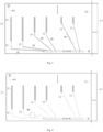
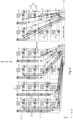
- Fig. 1 is a schematic planar structural diagram of a drive backplane provided by an embodiment of the present disclosure.
- the drive backplane provided by the embodiment of the present disclosure may include: a plurality of strip-shaped lamp regions (such as lamp regions W1, W2, W3 and W4 in Fig. 1 ) which extend in a first direction F1 and are arranged in a second direction F2, and a binding region B.
- the first direction F1 and the second direction F2 intersect with each other.
- Fig. 2 is a partially enlarged schematic diagram of a drive backplane provided by an embodiment of the present disclosure.
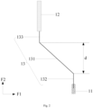
- the above drive backplane may further include:
- a distance, in a direction perpendicular to the first direction F1, between the two ends of the oblique line portion 131 is a first distance d.
- the first distances d of at least two oblique line portions 131 are different.
- the fan-out lines are arranged for coupling the signal lines to the corresponding binding electrodes. Moreover, there are at least two signal lines having different lengths in the second direction, and there are at least two oblique line portions having different first distances, so that the fan-out lines overlap at least one lamp region, a space of the lamp regions is fully utilized, and a fan-out region does not need to be set separately for take-up, which increases a wiring space of the drive backplane and reduces a bezel of a display apparatus.
- each lamp region is provided with a plurality of light emitting diodes.
- the light emitting diodes are coupled to at least one signal line 12.
- the binding region B is generally located at an edge position of the drive backplane.
- the binding region B includes a plurality of binding electrodes.
- the binding electrodes may be bound and connected with elements such as a drive chip or a flexible printed circuit.
- the binding electrodes are coupled to the signal lines through the fan-out lines. Therefore, signals may be applied to the signal lines through the drive chip or the flexible printed circuit, so as to control the light emitting diodes to emit light.
- the quantity and sizes of the binding electrodes in the binding region B need to match with the elements such as the drive chip or the flexible printed circuit.
- the sizes of the elements such as the drive chip or the flexible printed circuit are generally set as small as possible, so a width of the binding region B is usually smaller than a side width of the drive backplane.
- the signal lines 12 extend in the second direction F2. Moreover, in order to meet an electrical transmission capability and stability of the drive backplane for the signal lines 12, each signal line 12 has a certain width. Further, a width size of each binding electrode in the binding region is much smaller than the line width of the signal line. Therefore, the signal lines 12 cannot be directly connected to the binding region B with an unchanged width.
- the plurality of fan-out lines 13 are set. Each fan-out line 13 includes an oblique line portion and a first straight line portion. Therefore, the signal lines 12 may be connected with the binding electrodes in the binding region B through the fan-out lines 13.
- a width of one end of the oblique line portion 131 away from the binding electrode 11 may be set to be greater than a width of another end of the oblique line portion 131 close to the binding electrode 11.
- the width of the end of the oblique line portion 131 close to the binding electrode 11 may be set to be greater than a width of the first straight line portion 132.
- At least one fan-out line 13 among the plurality of fan-out lines may further include: a second straight line portion 133 extending in the second direction F2.
- One end of the second straight line portion 133 is coupled to one end of the signal line 12 close to the binding electrode 11, and the other end of the second straight line portion 133 is coupled to one end of the oblique line portion 131 away from the first straight line portion 132.
- each signal line 12 may be coupled to the corresponding binding electrode 11 through the corresponding fan-out line 13.
- a certain distance may be kept between adjacent fan-out lines 13 to avoid the intersection between the adjacent fan-out lines 13, so that the wiring space of the lamp regions may be utilized more reasonably, and the reliability of an electrical connection path is ensured.
- the drive backplane includes two first side edges L1 which extend in the second direction F2 and are oppositely arranged, and the drive backplane has a first axis L2 extending in the second direction F2 between the two first side edges L1.
- a length of the signal line 12 close to the first side edge L1 is greater than a length of the signal line 12 close to the first axis L2.
- a length of a signal line 12 on the leftmost side is greater than a length of a signal line 12 on the rightmost side.
- a first distance of the oblique line portion of the fan-out line 13 close to the first side edge L1 is smaller than a first distance of the oblique line portion of the fan-out line 13 close to the first axis L2.
- a first distance of the oblique line portion of a fan-out line 13 on the leftmost side is smaller than a first distance of the oblique line portion of a fan-out line 13 on the rightmost side.
- the length of each signal line 12 tends to decrease gradually, and the first distance d of the oblique line portion 131 of each fan-out line 13 tends to increase gradually.
- the gradually decreasing trend includes a case where a size relationship includes smaller than or equal to, and the gradually increasing trend includes a case where the size relationship includes greater than or equal to.
- each signal line 12 can be connected to the binding region B through the fan-out lines 13, and the space of the lamp regions may be utilized more reasonably.
- the oblique line portions 131 are symmetrically distributed with respect to the first axis L2. That is, the first axis L2 may be a central axis of the drive backplane, and the fan-out lines 13 are set to be symmetrically distributed, so that the signal lines 12 may be connected to the binding region B through the fan-out lines 13. There will be no intersection among the fan-out lines 13, and the space of the lamp regions is fully utilized.
- the oblique line portions being symmetrically distributed with respect to the first axis means that the first distances of two symmetrical oblique line portions are approximately equal. That is, a difference between the first distances of the two symmetrical oblique line portions is within a certain range.
- the fan-out lines 13 in the drive backplane may also be set to be asymmetrically distributed and may set according to an actual wiring situation, which is not limited here.
- the drive backplane includes a plurality of light emitting regions P arranged in an array in the first direction F1 and the second direction F2.
- the lamp region includes a plurality of light emitting regions P arranged in the first direction F 1.
- the plurality of signal lines may be divided into a plurality of signal line groups (for example, in Fig. 1 , signal lines 12 corresponding to one brace Q form a signal line group).
- Each signal line group Q at least includes a plurality of signal lines coupled to at least one row of light emitting regions P arranged in the second direction F2.
- a situation that each signal line group Q includes a plurality of signal lines coupled to two rows of light emitting regions P arranged in the second direction F2 is taken as an example for illustration.
- each signal line group Q may also include a plurality of signal lines coupled to three, four or more rows of light emitting regions P, which is not limited here.
- a difference between the first distances of different oblique line portions 131 coupled to signal lines 12 in the same signal line group Q is smaller than a set value, and a difference between the first distances of different oblique line portions 131 coupled to signal lines 12 in different signal line groups Q is greater than the set value.
- the set value may be a width of a lamp region in the second direction F2 or one half of the width of the lamp region in the second direction F2, which may be set according to the actual situation. That is, in the same signal line group Q, the first distances of the oblique line portions 131 coupled to the signal lines 12 are approximately equal, while the difference between the first distances of different oblique line portions 131 coupled to the signal lines 12 in different signal line groups Q is large.
- the first distances of the oblique line portions 131 coupled to the signal lines 12 are all smaller than the width of one lamp region in the second direction F2.
- the first distances of the oblique line portions 131 coupled to the signal lines 12 are all greater than the width of one lamp region in the second direction F2, and smaller than twice the width of the lamp region in the second direction F2.
- a difference between the first distance of the oblique line portion 131 coupled to any signal line 12 in the first signal line group Q on the left side and the first distance of the oblique line portion 131 coupled to any signal line 12 in the second signal line group Q on the left side is greater than the width of one lamp region in the second direction F2.
- the first distances of the oblique line portions 131 of the fan-out lines 13 coupled to the signal lines 12 in the same signal line group Q are approximately equal, which is more conducive to the wiring of the drive backplane and makes the wiring in the drive backplane more regular.
- a width of at least one signal line 12 among the plurality of signal lines 12 is greater than a width of the fan-out line 13.
- the line width of the signal line 12 is set to be large, so that a resistance of the signal line 12 may be reduced, a phenomenon of signal delay is avoided, and the performance of the drive backplane is improved.
- the binding region B is generally set at a middle position of an edge of the drive backplane. Therefore, the closer the signal lines 12 to the first side edges L1, the farther they are from the binding region B. If the widths of the signal lines 12 and the fan-out lines 13 are the same, the difference between a resistance sum of the signal lines 12 close to the first side edges L1 and the fan-out lines 13 and a resistance sum of the signal lines 12 close to the middle position and the fan-out lines 13 is large, which is prone to signal delay, and poor effects of uneven display brightness and the like are caused. In the embodiments of the present disclosure, the width of each signal line 12 is enlarged.
- the length of the signal line 12 close to the first side edge L1 is greater than the length of the signal line 12 close to the first axis L2.
- the following methods may be at least adopted to realize an equal resistance design of each channel.
- Fig. 3 is another schematic planar structural diagram of a drive backplane provided by an embodiment of the present disclosure.
- an auxiliary connecting line 50 is at least set at a position close to the first side edge L1.
- the auxiliary connecting line 50 and the corresponding fan-out line 13 form a double-layer parallel line.
- the auxiliary connecting lines 50 may be set at the positions where the oblique line portions of the corresponding fan-out lines 13 are located.
- the auxiliary connecting lines 50 may be set in different layers with the fan-out lines 13.
- the auxiliary connecting lines 50 may be set in the same layer with other film layers in the drive backplane.
- the auxiliary connecting line(s) 50 may be set at the position close to the first side edge L1, while no auxiliary connecting line 50 is set at the position close to the first axis L2. That is, the fan-out lines 13 at the middle position are single-layer lines. Moreover, in a direction each first side edge L1 pointing to the first axis L2, a length of each auxiliary connecting line 50 gradually decreases.
- Fig. 4 is another schematic planar structural diagram of a drive backplane provided by an embodiment of the present disclosure.
- a broken line structure 60 is at least set in the fan-out line 13 close to the first axis L2.
- the broken line structure 60 included in each fan-out line 13 gradually decreases.
- the broken line structure 60 may be set at position of the oblique line portion, the first straight line portion or the second straight line portion in the fan-out line 13.
- Fig. 4 is only intended to illustrate an approximate position of the broken line structure 60, and does not limit the size and shape of the fan-out line 13.
- the equal resistance design of each channel is illustrated by taking the above method 1 and method 2 as examples.
- the above method 1 and method 2 may also be combined, or other methods may also be adopted, as long as the resistance of each channel can be consistent, which is not limited here.
- the above drive backplane provided by the embodiments of the present disclosure may further include: a plurality of first contact electrode groups 14 and a plurality of second contact electrode groups which are located on the base substrate (a region K in Fig. 1 represents a region where each second contact electrode group in a light emitting region P is located).
- Fig. 5 is a partially enlarged schematic diagram of one light emitting region in the embodiments of the present disclosure, in combination with Fig. 1 and Fig. 5 , each light emitting region P is provided with a first contact electrode group 14 and at least three second contact electrode groups 15.
- the first contact electrode group 14 includes a plurality of first contact electrodes 141 configured to be coupled to pins of a pixel drive chip.
- the second contact electrode group 15 includes: two second contact electrodes 151 configured to be coupled to electrodes of a light emitting diode.
- the second contact electrode groups 15 are coupled through a connecting line 16.
- the pixel drive chips are bound to the positions of the first contact electrode groups 14, the pins of the pixel drive chips are coupled to the first contact electrodes 141, the light emitting diode is bound to the positions of the second contact electrode groups 15, and the electrodes of the light emitting diode are coupled to the second contact electrodes 151. It may be understood that light emitting diodes of different colors connected in parallel are bound into the same light emitting region P, thereby achieving color display.
- each light emitting region P is provided with four second contact electrode groups 15 is taken as an example for illustration.
- the quantity of the second contact electrode groups 15 in each light emitting region P may be set according to actual needs, which is not limited here.
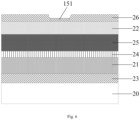
- Fig. 6 is a schematic sectional view of Fig. 5 at a dotted line T.
- the signal lines (a film layer 21 in Fig. 6 ) are located between a film layer where the second contact electrodes 151 are located and the base substrate 20.
- the first contact electrodes and the second contact electrodes may be located on the same film layer to save a production process.
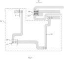
- Fig. 7 is a partially enlarged schematic diagram of a drive backplane in an embodiment of the present disclosure. In combination with Fig. 6 and Fig.
- orthographic projections of the second contact electrodes 151 on the base substrate 20 are located within a range of an orthographic projection of at least one signal line 12 among the plurality of signal lines 12 on the base substrate 20.
- the signal lines 12 are set below the second contact electrodes 151 respectively, and the situation that there is a segment difference between the two second contact electrodes 151 in one second contact electrode group, leading to an uneven surface of the second contact electrodes 151 to be bound and connected to the light emitting diode, thereby affecting a light emitting direction of the light emitting diode, the reliability of the binding and a display effect is avoided.
- the orthographic projections of the second contact electrodes 151 on the base substrate are all located within the range of the orthographic projection of the same signal line 121 on the base substrate.
- one part of the orthographic projections of the second contact electrodes 151 on the base substrate is within the range of the orthographic projections of the signal lines on the base substrate, and the other part is located between two adjacent signal lines.
- Dotted boxes H1 and H2 in Fig. 7 represent outlines of two adjacent signal lines without convex and concave portions, and each second contact electrode 151 includes two sub-electrodes 151a and 151b. It can be clearly seen that an orthographic projection of the second contact electrode 151a on the base substrate is located in a gap between the two signal lines.
- the shape of a region corresponding to the signal line 121 having a largest overlapping area with the second contact electrode 151 is adjusted, and the shape of the signal line 122 closest to the signal line 121 is adaptively adjusted, so that it is ensured that the second contact electrode 151 is above a pattern of the same signal line 121, surfaces of all regions of the second contact electrode 151 are flatter, the reliability of the light emitting diode bound and connected to the second contact electrode 151 is better, and the light emitting direction of the light emitting diode cannot be affected.
- the two adjacent signal lines have a concave portion and a convex portion respectively
- the spacing of the two signal lines at each position is approximately the same, and thus, the setting of the convex portion and the concave portion cannot generate an electrical interference between the signal lines.
- Fig. 8 is another schematic planar structural diagram of a drive backplane provided by an embodiment of the present disclosure.
- the plurality of signal lines may include: a plurality of first power signal lines 121, a plurality of second power signal lines 122, a plurality of fixed voltage signal lines 123 and a plurality of addressing signal lines 124.
- the first power signal lines 121 are coupled to the second contact electrodes (located in a region K in Fig. 8 ) in a row of the light emitting regions P arranged in the second direction F2.
- the second power signal lines 122 are coupled to the first contact electrodes (located in the first contact electrode group 14) in a row of the light emitting regions P arranged in the second direction F2.
- the fixed voltage signal lines 123 are coupled to the first contact electrodes in a row of the light emitting regions P arranged in the second direction F2.
- the addressing signal lines 124 are coupled to the first contact electrodes in two adjacent rows of the light emitting regions P arranged in the second direction F2.
- Fig. 9 is an equivalent circuit diagram of the light emitting region shown in Fig. 5 . Moreover, in order to illustrate a connection relationship of the respective signal lines, Fig. 9 illustrates a connection relationship after the drive backplane is bound to the light emitting diode and a pixel driving circuit.
- the pixel drive chip 17 may include a first input end Di, a second input end pwr, an output end Ou and a common voltage end Gn.
- the light emitting diodes 18 in the light emitting region P are sequentially connected in series.
- a first light emitting diode 18 connected in series is connected with the first power signal lines 121
- the last light emitting diode 18 connected in series is connected with the output end Ou of the pixel drive chip 17, and power may be supplied to each light emitting diode 18 in the light emitting region P through the first power signal lines 121.
- the first power signal lines 121 are coupled to one row of the light emitting regions P arranged in the second direction F2, which may supply power to the light emitting diodes 18 in the one row of the light emitting regions P.
- the second power signal lines 122 are connected with the second input end pwr of the pixel drive chip 17, and power may be supplied to the pixel drive chip 17 through the second power signal lines 121.
- the second power signal lines 122 are coupled to one row of the light emitting regions P arranged in the second direction F2, which may supply power to the pixel drive chip 17 in the one row of the light emitting regions P.
- the fixed voltage signal lines 123 are connected with the common voltage end Gn of the pixel drive chip 17, and common voltage signals are supplied to the pixel drive chip 17 through the fixed voltage signal lines 123.
- the common voltage signals may be grounding signals.
- the fixed voltage signal lines 123 are coupled to one row of the light emitting regions P arranged in the second direction F2, which may supply common voltage signals to the pixel drive chip 17 in the one row of the light emitting regions P.
- the addressing signal lines 124 are connected with the first input end Di of the pixel drive chip 17.
- the addressing signal lines 124 may transmit address signals to the pixel drive chip 17, and the pixel drive chip 17 may obtain a transmitted address by analyzing the address signals.
- the pixel drive chips 17 in two adjacent rows of the light emitting regions P arranged in the second direction F2 are sequentially connected in series.
- the addressing signal lines 124 are connected with a first input end Di of a first pixel drive chip 17 connected in series; an output end Ou of an m th pixel drive chip 17 connected in series is connected with a first input end Di of an (m+1) th pixel drive chip 17 connected in series, m is a positive integer greater than 0 and smaller than n, and n is the quantity of the two adjacent rows of the light emitting regions P arranged in the second direction F2.
- the plurality of above signal lines 12 may further include a plurality of addressing connecting lines 125. An output end Ou of the last pixel drive chip 17 connected in series is coupled to the addressing signal lines 125, so as to form a loop for transmitting the address signals
- Fig. 6 is a schematic sectional view of Fig. 5 at a dotted line T.
- the drive backplane in the embodiments of the present disclosure may include: a first metal layer 21 located on the base substrate 20, a second metal layer 22 located on one side of the first metal layer 21 facing away from the base substrate 20, a buffer layer 23 located between the first metal layer 21 and the base substrate 20, an inorganic layer 24 located between the first metal layer 21 and the second metal layer 22, and a planarization layer 25 located between the inorganic layer 24 and the second metal layer 22.
- the respective signal lines 12 may be located on the same film layer.
- the respective connecting lines 16 may be located in the same film layer.
- the respective signal lines 12 may be located in the first metal layer 21, and the respective connecting lines 16 may be located in the second metal layer 22.
- the inorganic layer 24 is arranged between the first metal layer 21 and the second metal layer 22, the sealing property of the drive backplane may be improved, the erosion of the drive backplane by water vapor and oxygen is prevented.
- the planarization layer 25 may also prevent the first metal layer 21 from being oxidized at a high temperature.
- the planarization layer 25 is arranged between the inorganic layer 24 and the second metal layer 22, so that the second metal layer 22 may be flatter.
- the signal lines 12 may be electrically connected with the connecting lines 16 through via hole(s) V penetrating through the inorganic layer 24 and the planarization layer 25.
- the first metal layer 21 and the second metal layer 22 may be made of metal materials, such as metal copper or other metal materials, which is not limited here.
- the above drive backplane provided by the embodiments of the present disclosure may further include: an inorganic insulating layer 26 located on one side of the connecting lines (a film layer where the second metal layer 22 is located) facing away from the base substrate 20.
- the thickness of the inorganic insulating layer 26 is greater than 2000 ⁇ .
- the thickness of the inorganic insulating layer 26 may be set to about 5000 ⁇ .
- the sealing property of the drive backplane may be further improved, the erosion of the drive backplane by the water vapor and the oxygen is prevented.
- a planarization layer does not need to be arranged on one side of the inorganic insulating layer 26 facing away from the base substrate 20, so as to prevent the first contact electrodes (not shown in the figure) and the second contact electrodes 151 from being oxidized after the planarization layer absorbs water.
- patterns of the first contact electrodes and the second contact electrodes may be directly formed, and a process of manufacturing the planarization layer is saved, and the manufacturing costs are saved.
- Fig. 10 is a schematic structural diagram of a light emitting region group in the embodiments of the present disclosure. As shown in Fig. 10 , each light emitting region group includes two adjacent rows of the light emitting regions P arranged in the second direction F2.
- a first contact electrode group 14 is located in a partial region in the light emitting region P away from the binding electrode; and in the other row of light emitting regions P (such as a row of light emitting regions P on the right side in Fig. 10 ) of the light emitting region group, the first contact electrode group 14 is located in a partial region in the light emitting region P close to the binding electrode.
- the signal lines are coupled to the corresponding binding electrodes through the fan-out lines. Moreover, there are at least two signal lines having different lengths in the second direction, and there are at least two oblique line portions having different first distances, thus a fan-out region does not need to be set separately for take-up. Therefore, several lamp regions close to the binding region have enough spaces to set the first contact electrode groups 14, the second contact electrode groups 15 and the connecting lines 16.
- the winding of the connecting lines 16 may be set to make the arrangement of the first contact electrode groups 14 and the second contact electrode groups 15 more regular, thereby facilitating a binding process and an optical detection process for the light emitting diode and the pixel drive chip, and improving the efficiency of the binding process and the optical detection process.
- the obtained electrical and optical homogeneity of the display apparatus may be better, and the display effect is improved.
- a plurality of connecting lines are arranged on a film layer between the signal lines and the first contact electrodes.
- part of the plurality of connecting lines 16 are configured to connect the signal lines 12 with the first contact electrodes 141, part of the plurality of connecting lines 16 are configured to connect the signal lines 12 with the second contact electrodes 151, part of the plurality of connecting lines 16 are configured to connect the first contact electrodes 141 with the second contact electrodes 151, part of the plurality of connecting lines 16 are configured to connect two first contact electrodes 141, and part of the plurality of connecting lines 16 are configured to connect two second contact electrodes 151.
- At least part of the plurality of connecting lines 16 include: a first connecting portion 161 extending in the first direction F1 and a second connecting portion 162 extending in the second direction F2. Due to the large quantity of connecting lines 16 in the drive backplane, the connecting lines 16 are set to extend in the first direction F1 or the second direction F2, a phenomenon that the connecting lines 16 intersect with each other can be avoided, which is more conducive to wiring, and the wiring space in the drive backplane is fully utilized.
- the position where the first connecting portion 161 is connected with the second connecting portion 162 in each connecting line 16 has a fillet setting, so as to avoid tip discharge.
- the fillet setting may be performed on one side of the position where the first connecting portion 161 is connected with the second connecting portion 162, and the fillet setting may also be performed on two sides of the position.
- the following methods are schematically provided to prepare the above drive backplane, but they should not limit a preparation method of the above drive backplane.
- the buffer layer 23 is manufactured on the base substrate 20.
- the first metal layer 21 is formed on the buffer layer 23 by adopting a sputtering process.
- a material of the first metal layer 21 may be metal copper.
- the first metal layer 21 is coated with a photoresist layer, and processes of baking, exposure, development, hard baking and the like are performed on the photoresist layer, so as to obtain a pattern of the photoresist layer.
- the first metal layer 21 is etched under a mask of the pattern of the photoresist layer, and then, a pattern of the first metal layer 21 is obtained after the photoresist layer is peeled off.
- the inorganic layer 24 is formed on the first metal layer 21, for example, the inorganic layer 24 may be manufactured by adopting a process such as chemical vapor deposition.
- the planarization layer 25 is coated with the inorganic layer 24, and the processes of exposure, development and the like are performed on the planarization layer 25, so as to form a pattern of the planarization layer 25, and then, the inorganic layer 24 is dry-etched under a mask of the pattern of the planarization layer 25, so as to obtain a pattern of the inorganic layer 24.
- a material of the second metal layer 22 may be metal copper.
- the second metal layer 22 is coated with a photoresist layer, and processes of baking, exposure, development, hard baking and the like are performed on the photoresist layer, so as to obtain a pattern of the photoresist layer.
- the second metal layer 22 is etched under a mask of the pattern of the photoresist layer, and then, a pattern of the second metal layer 22 is obtained after the photoresist layer is peeled off.
- An inorganic insulating layer 26 is formed on the second metal layer 22, then the inorganic insulating layer 26 is coated with a photoresist layer, and processes of baking, exposure, development and the like are performed on the photoresist layer. Then, the inorganic insulating layer 26 is dry-etched under a mask of the pattern of the photoresist layer, so as to obtain a pattern of the inorganic insulating layer 26. Finally, each first contact electrode and each second contact electrode are formed on the inorganic insulating layer 26.
- the difference from the above process steps is that a second manufacturing method adopts an electroplating process to form the pattern of the first metal layer.
- the sputtering process is firstly adopted to form an electroplating seed layer on the base substrate 20.
- a material of the electroplating seed layer may be metal copper.
- a photoresist layer is formed on the electroplating seed layer, and processes of baking, exposure, development, hard baking and the like are performed on the photoresist layer, so as to obtain a pattern of the photoresist layer.
- the electroplating seed layer is etched under a mask of the pattern of the photoresist layer, and then, a pattern of the electroplating seed layer is obtained after the photoresist layer is peeled off.
- the pattern of the first metal layer 21 is formed by adopting an electroplating process.
- Embodiments of the present disclosure further provide a display apparatus, including: any above drive backplane, and a plurality of pixel drive chips and a plurality of light emitting diodes which are coupled to the drive backplane.
- the display apparatus may be applied to a mobile phone, a tablet computer, a television, a display, a laptop, a digital photo frame, a navigator and any product or component with a display function. Since the principle for solving problems of the display apparatus is similar to that of the above drive backplane, implementation of the display apparatus may refer to implementation of the above drive backplane, and repetitions are omitted herein.
Landscapes
- Devices For Indicating Variable Information By Combining Individual Elements (AREA)
- Electroluminescent Light Sources (AREA)
Applications Claiming Priority (1)
| Application Number | Priority Date | Filing Date | Title |
|---|---|---|---|
| PCT/CN2020/139494 WO2022134019A1 (zh) | 2020-12-25 | 2020-12-25 | 驱动背板及显示装置 |
Publications (2)
| Publication Number | Publication Date |
|---|---|
| EP4145432A1 true EP4145432A1 (de) | 2023-03-08 |
| EP4145432A4 EP4145432A4 (de) | 2023-09-13 |
Family
ID=82157144
Family Applications (1)
| Application Number | Title | Priority Date | Filing Date |
|---|---|---|---|
| EP20966584.3A Pending EP4145432A4 (de) | 2020-12-25 | 2020-12-25 | Treiberrückwand und anzeigevorrichtung |
Country Status (4)
| Country | Link |
|---|---|
| US (1) | US20230207761A1 (de) |
| EP (1) | EP4145432A4 (de) |
| CN (1) | CN114981868B (de) |
| WO (1) | WO2022134019A1 (de) |
Families Citing this family (2)
| Publication number | Priority date | Publication date | Assignee | Title |
|---|---|---|---|---|
| CN117918030A (zh) * | 2022-08-19 | 2024-04-23 | 京东方科技集团股份有限公司 | 基板和电子装置 |
| CN119673061B (zh) * | 2023-09-20 | 2025-10-17 | 合肥京东方瑞晟科技有限公司 | 背光模组和显示装置 |
Family Cites Families (16)
| Publication number | Priority date | Publication date | Assignee | Title |
|---|---|---|---|---|
| KR200162435Y1 (ko) * | 1993-06-21 | 1999-12-15 | 손욱 | 슈퍼트위스트네마틱 액정 디스플레이 |
| GB0411970D0 (en) * | 2004-05-28 | 2004-06-30 | Koninkl Philips Electronics Nv | Non-rectangular display device |
| US20070216845A1 (en) * | 2006-03-16 | 2007-09-20 | Chia-Te Liao | Uniform impedance conducting lines for a liquid crystal display |
| KR20070117268A (ko) * | 2006-06-08 | 2007-12-12 | 삼성전자주식회사 | 박막 트랜지스터 기판 및 이를 포함하는 액정 표시판 |
| TWI464484B (zh) * | 2011-12-02 | 2014-12-11 | 友達光電股份有限公司 | 扇出線路以及具有此扇出線路的電子裝置 |
| KR102354970B1 (ko) * | 2015-06-22 | 2022-01-25 | 삼성디스플레이 주식회사 | 디스플레이 장치 |
| CN106597713B (zh) * | 2017-01-22 | 2020-03-24 | 厦门天马微电子有限公司 | 一种阵列基板和显示面板 |
| CN207781596U (zh) * | 2017-12-14 | 2018-08-28 | 京东方科技集团股份有限公司 | 一种阵列基板及显示装置 |
| CN208077535U (zh) * | 2018-04-28 | 2018-11-09 | 京东方科技集团股份有限公司 | 一种柔性显示面板及柔性显示装置 |
| CN108878453A (zh) * | 2018-06-29 | 2018-11-23 | 上海天马微电子有限公司 | 一种阵列基板、显示面板及显示装置 |
| US11037980B2 (en) * | 2018-08-10 | 2021-06-15 | Sharp Kabushiki Kaisha | Image display device |
| WO2020071010A1 (ja) * | 2018-10-02 | 2020-04-09 | 株式会社ジャパンディスプレイ | 表示装置 |
| CN110412802A (zh) * | 2019-06-27 | 2019-11-05 | 厦门天马微电子有限公司 | 显示面板和显示装置 |
| CN210575035U (zh) * | 2019-11-29 | 2020-05-19 | 云谷(固安)科技有限公司 | 一种阵列基板及显示面板 |
| CN113066408B (zh) * | 2020-01-02 | 2025-04-08 | 京东方科技集团股份有限公司 | 一种显示基板及其制作方法、显示装置 |
| CN111933674B (zh) * | 2020-08-18 | 2024-06-11 | 京东方科技集团股份有限公司 | 显示基板和显示装置 |
-
2020
- 2020-12-25 WO PCT/CN2020/139494 patent/WO2022134019A1/zh not_active Ceased
- 2020-12-25 CN CN202080003699.0A patent/CN114981868B/zh active Active
- 2020-12-25 EP EP20966584.3A patent/EP4145432A4/de active Pending
- 2020-12-25 US US18/000,198 patent/US20230207761A1/en active Pending
Also Published As
| Publication number | Publication date |
|---|---|
| WO2022134019A1 (zh) | 2022-06-30 |
| CN114981868A (zh) | 2022-08-30 |
| EP4145432A4 (de) | 2023-09-13 |
| US20230207761A1 (en) | 2023-06-29 |
| CN114981868B (zh) | 2024-04-02 |
Similar Documents
| Publication | Publication Date | Title |
|---|---|---|
| US11004382B2 (en) | Backlight source and manufacture method thereof, display device | |
| US12266642B2 (en) | Light-emitting substrate, backlight, display device | |
| US12404995B2 (en) | Backlight module and display device | |
| US20250174544A1 (en) | Light-emitting substrate and display apparatus | |
| TWI642979B (zh) | 背光裝置 | |
| US12525568B2 (en) | Backplane and glass-based circuit board | |
| EP4340566A1 (de) | Lichtemittierendes substrat und herstellungsverfahren dafür, rückbeleuchtungsquelle und anzeigevorrichtung | |
| US12087698B2 (en) | Wiring substrate, array substrate and light emitting module having control regions arranged into control region rows and control region columns | |
| US12256617B2 (en) | Display panel and display device | |
| EP4145432A1 (de) | Treiberrückwand und anzeigevorrichtung | |
| WO2023109233A1 (zh) | 发光二极管驱动背板及显示装置 | |
| US20240128278A1 (en) | Bonding structure, display panel, flexible circuit board and display apparatus | |
| CN121142838A (zh) | 灯板和显示设备 | |
| CN119731589A (zh) | 基板和电子装置 | |
| EP4542649A1 (de) | Grundplatte und elektronische vorrichtung | |
| CN120419327A (zh) | 布线基板、其制作方法及电子装置 | |
| US12575234B2 (en) | Light-emitting substrate and manufacturing method thereof, and display device | |
| US20240234434A1 (en) | Drive Backplane, Preparation Method therefor, and Display Apparatus | |
| JP2023531341A (ja) | 表示基板及び表示装置 | |
| CN115720468B (zh) | 显示面板和显示设备 | |
| CN117496835A (zh) | 一种显示模组及其拼接方法、显示装置 | |
| WO2026081071A1 (zh) | 发光基板、背光模组和显示装置 | |
| CN120599946A (zh) | 一种显示面板及显示装置 | |
| CN120530734A (zh) | 布线基板及其制备方法、发光基板、显示装置 | |
| WO2022205343A1 (zh) | 发光基板及显示装置 |
Legal Events
| Date | Code | Title | Description |
|---|---|---|---|
| STAA | Information on the status of an ep patent application or granted ep patent |
Free format text: STATUS: THE INTERNATIONAL PUBLICATION HAS BEEN MADE |
|
| PUAI | Public reference made under article 153(3) epc to a published international application that has entered the european phase |
Free format text: ORIGINAL CODE: 0009012 |
|
| STAA | Information on the status of an ep patent application or granted ep patent |
Free format text: STATUS: REQUEST FOR EXAMINATION WAS MADE |
|
| 17P | Request for examination filed |
Effective date: 20221130 |
|
| AK | Designated contracting states |
Kind code of ref document: A1 Designated state(s): AL AT BE BG CH CY CZ DE DK EE ES FI FR GB GR HR HU IE IS IT LI LT LU LV MC MK MT NL NO PL PT RO RS SE SI SK SM TR |
|
| REG | Reference to a national code |
Ref country code: DE Ref legal event code: R079 Free format text: PREVIOUS MAIN CLASS: G09F0009330000 Ipc: H01L0025075000 |
|
| A4 | Supplementary search report drawn up and despatched |
Effective date: 20230814 |
|
| RIC1 | Information provided on ipc code assigned before grant |
Ipc: H01L 23/528 20060101ALI20230808BHEP Ipc: G02F 1/1345 20060101ALI20230808BHEP Ipc: G09F 9/33 20060101ALI20230808BHEP Ipc: H01L 33/62 20100101ALI20230808BHEP Ipc: H01L 25/075 20060101AFI20230808BHEP |
|
| DAV | Request for validation of the european patent (deleted) | ||
| DAX | Request for extension of the european patent (deleted) |