EP4142145B1 - Control circuit for an electric motor and controlling method thereof - Google Patents
Control circuit for an electric motor and controlling method thereof Download PDFInfo
- Publication number
- EP4142145B1 EP4142145B1 EP21193885.7A EP21193885A EP4142145B1 EP 4142145 B1 EP4142145 B1 EP 4142145B1 EP 21193885 A EP21193885 A EP 21193885A EP 4142145 B1 EP4142145 B1 EP 4142145B1
- Authority
- EP
- European Patent Office
- Prior art keywords
- current
- gain
- control circuit
- signal
- phase
- Prior art date
- Legal status (The legal status is an assumption and is not a legal conclusion. Google has not performed a legal analysis and makes no representation as to the accuracy of the status listed.)
- Active
Links
Images


Classifications
-
- H—ELECTRICITY
- H02—GENERATION; CONVERSION OR DISTRIBUTION OF ELECTRIC POWER
- H02P—CONTROL OR REGULATION OF ELECTRIC MOTORS, ELECTRIC GENERATORS OR DYNAMO-ELECTRIC CONVERTERS; CONTROLLING TRANSFORMERS, REACTORS OR CHOKE COILS
- H02P29/00—Arrangements for regulating or controlling electric motors, appropriate for both AC and DC motors
- H02P29/40—Regulating or controlling the amount of current drawn or delivered by the motor for controlling the mechanical load
-
- H—ELECTRICITY
- H02—GENERATION; CONVERSION OR DISTRIBUTION OF ELECTRIC POWER
- H02P—CONTROL OR REGULATION OF ELECTRIC MOTORS, ELECTRIC GENERATORS OR DYNAMO-ELECTRIC CONVERTERS; CONTROLLING TRANSFORMERS, REACTORS OR CHOKE COILS
- H02P25/00—Arrangements or methods for the control of AC motors characterised by the kind of AC motor or by structural details
- H02P25/02—Arrangements or methods for the control of AC motors characterised by the kind of AC motor or by structural details characterised by the kind of motor
- H02P25/06—Linear motors
-
- G—PHYSICS
- G01—MEASURING; TESTING
- G01R—MEASURING ELECTRIC VARIABLES; MEASURING MAGNETIC VARIABLES
- G01R19/00—Arrangements for measuring currents or voltages or for indicating presence or sign thereof
- G01R19/0092—Measuring current only
-
- H—ELECTRICITY
- H03—ELECTRONIC CIRCUITRY
- H03K—PULSE TECHNIQUE
- H03K3/00—Circuits for generating electric pulses; Monostable, bistable or multistable circuits
- H03K3/02—Generators characterised by the type of circuit or by the means used for producing pulses
- H03K3/027—Generators characterised by the type of circuit or by the means used for producing pulses by the use of logic circuits, with internal or external positive feedback
- H03K3/037—Bistable circuits
-
- H—ELECTRICITY
- H03—ELECTRONIC CIRCUITRY
- H03M—CODING; DECODING; CODE CONVERSION IN GENERAL
- H03M1/00—Analogue/digital conversion; Digital/analogue conversion
- H03M1/12—Analogue/digital converters
- H03M1/18—Automatic control for modifying the range of signals the converter can handle, e.g. gain ranging
-
- H—ELECTRICITY
- H02—GENERATION; CONVERSION OR DISTRIBUTION OF ELECTRIC POWER
- H02P—CONTROL OR REGULATION OF ELECTRIC MOTORS, ELECTRIC GENERATORS OR DYNAMO-ELECTRIC CONVERTERS; CONTROLLING TRANSFORMERS, REACTORS OR CHOKE COILS
- H02P2205/00—Indexing scheme relating to controlling arrangements characterised by the control loops
- H02P2205/01—Current loop, i.e. comparison of the motor current with a current reference
Definitions
- the present invention relates to the field of electric motors and more particularly to a control circuit for an electric motor and a motor comprising such control circuit.
- the present invention further relates to a method for controlling the control circuit to achieve precise and accurate driving of electric motors.
- Electric motors used in various industrial installations are often controlled to achieve a target position.
- a feedback loop is used to modify the actual position of a moving part of the motor such that it corresponds to the target position.
- the difference between the actual position and the target position is processed by an electronic control unit, which determines a target supply current.
- the control unit of the motor is therefore adapted to supply the motor (each of its phases) in such a way as to generate a supply current corresponding to the target supply current to achieve high precision positioning of the moving part of the motor.
- US8860354B2 discloses a control circuit for an electric motor, which is configured to generate via a first digital-to-analog converter, a control signal for driving the electric motor.
- the control circuit comprises a low-voltage zone and a high-voltage zone.
- the low-voltage zone comprises a control unit while the high-voltage zone comprises a current sensor for measuring the current supply to the electric motor and an analog-to-digital converter (ADC) to convert the analog signal into a corresponding digital signal which is sent to the control unit.
- a galvanic separating element is provided between the low and high-voltage zones for security reasons.
- the noise level on the output current I output is crucial and is usually expressed in ⁇ Arms.
- the noise level is directly linked to the current measurement's least significant bit (LSB) resolution.
- the LSB resolution may be reduced in three different ways:
- US9383734 discloses for example a control circuit for feedback-based control of motion and positioning of a motor.
- the control circuit comprises a current measurement device configured to obtain a measurement of the current in the phase load of the motor to provide feedback.
- the intensity of the current in the phase load varies within an operating range which is made up of a relatively large current range for the acceleration phase of the motor and of relatively smaller current range when the motor is at standstill or running at constant speed.
- the current measurement device has a first coarse sensor optimized for measuring the relatively large current range and a second fine sensor optimized for measuring the relatively smaller current range, thereby maximizing feedback accuracy when the motor is at standstill or running at constant speed.
- US6057664 discloses a motor driving control apparatus and a motor driving method.
- USJP5556353 discloses a motor control detection IC and a motor control device using the same.
- An aim of the present invention is to provide an alternative control circuit, for driving an electric motor, which optimizes the current feedback as a function of the operating range of the electric motor.
- Another aim of the present invention is to provide a control circuit with high and low voltage subcircuit separated by a galvanic isolation and adapted to use an isolator with a limited number of channels to pass control data across the galvanic isolation barrier for selecting a low or high gain driving modes.
- the control circuit comprises a low voltage subcircuit, a high voltage subcircuit and an isolation barrier between the low voltage and high voltage subcircuits.
- the low voltage subcircuit comprises a current controller adapted to generate a driving signal, and a feedback loop whose output is fed back to the input of the current controller.
- the high voltage subcircuit comprises a power bridge to output a current for driving the at least one phase of the motor, a current sensor for measuring the current in the at least one phase, an analog front-end and an analog-to-digital converter (ADC).
- ADC analog-to-digital converter
- the isolation barrier comprises an isolator adapted to pass the output signal of the ADC across the isolation barrier from the high voltage subcircuit to the low voltage subcircuit.
- the analog front-end is adapted to apply a first gain or a second gain that is higher than the first gain as a function of the current in the at least one phase measured by the current sensor.
- the isolator comprises a first and a second channel to pass respectively a clock signal and a control signal from the low voltage subcircuit to the high voltage subcircuit in order to select the first or second gain of the analog front-end.
- the isolator comprises a third and a fourth channel to pass respectively the output data of the ADC and a replica of the clock signal from the high voltage subcircuit to the low voltage subcircuit.
- the high voltage subcircuit further comprises a D flip-flop.
- the clock input of the D flip-flop is arranged to receive the control signal and the input of the D flip-flop is arranged to receive the clock signal.
- the output of the D flip-flop is used for selection of either first or second gain of the analog front-end as a function of the clock signal.
- the high voltage subcircuit further comprises a multiplexer comprising two data inputs and a selector input, wherein one of the two data inputs is arranged to receive the clock signal, the other of the two data inputs is arranged to receive the output of the D flip-flop.
- the selector input is arranged to receive the control signal such that either the selected gain or the replica of the clock signal may be passed via the fourth channel of the isolator based on the state of the control signal.
- the feedback loop of the low voltage subcircuit comprises a deserializer arranged to receive serial data from the ADC, representing the current value measured by the current sensor, as an input to convert the serial data into a single value encoded on M bits.
- the feedback loop also comprises a register shifter for changing the value of said M bits if the selected first or second gain differs from the gain applied to said current value.
- the feedback loop further comprises an accumulator arranged to add up different samples of currents measured by the current sensor, a decimator filter for sampling N current samples and a division element for outputting a moving average of the current measurements.
- the feedback loop further comprises a clock generator arranged to generate a first or a second clock signal as a function of the selected first or second gain.
- the selection of the first or second gain is based on the current measured by the current sensor.
- the clock generator is arranged to adapt the first and second clock signals, when the current measured by the current sensor is between a first and a second current thresholds, such that the moving average of the current measurement outputted by the division element is made up of current samples measured with the first gain and current samples measured with the second gain during a transition phase from a low to a high gain driving mode or from a high to a low gain driving mode.
- Another aspect of the invention relates to an electric motor comprising the control circuit as described above.
- a further aspect of the invention relates to a method for controlling the control circuit for an electric motor, comprising the steps of
- the transition phase is divided into N sub-transition phases.
- a first sub-transition phase is the sub-transition phase just above the first current threshold value.
- a last sub-transition phase is the sub-transition phase just below the second current threshold value.
- At least 90% of 100/N %, and preferably around 100/N % of the current measurement samples are taken during the first sub-transition phase with the second gain while the rest of the current measurement samples are taken during the first sub-transition phase with the first gain.
- At least 90% of 100 / N %, and preferably around 100/N % of the current measurement samples are taken during the last sub-transition phase with the first gain while the rest of the current measurement samples are taken during the last sub-transition phase with the second gain.
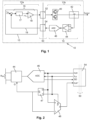
- FIG. 1 shows a simplified block diagram of a control circuit 10 for an electric motor having at least one phase according to an embodiment.
- the control circuit 10 comprises a low voltage subcircuit 12a, a high voltage subcircuit 12b and an isolation barrier 50 between the low voltage and high voltage subcircuits 12a, 12b.
- the low voltage subcircuit 12a has a digital signal processor 15 comprising a current controller 16.
- the digital signal processor can optionally be replaced by a programmable logic element such as a field programmable gate array (FPGA).
- the current controller 16 may comprise for example a PI controller 17 and a comparator 18 to output a PWM signal.
- the PI controller 17 is adapted to correct an error value based on a reference signal I ref and a feedback measurement value.
- a PID controller may however be used instead of the PI controller in an alternative embodiment.
- the high voltage subcircuit 12b comprises a power bridge 40 to control the electric motor, a current sensor 42 for measuring the current flowing in the at least one phase of the electric motor when operating, an analog-front-end 44 for signal conditioning of the current signal to exploit the full input range of an analog-digital converter (ADC) 46.
- the current sensor 42 is preferably a shunt resistance Rsh ( Figure 2 ). The current builds up a voltage across the shunt resistance Rsh. This voltage is then amplified by the analog front-end 44 and digitally converted by the ADC 46.
- the isolation barrier 50 is an essential element for safety reasons.
- the isolation barrier comprises a gate driver 52 to produce a high-current drive input for the gate of the transistors of the power bridge 40 and an isolator 54 so that the serial data outputted by the ADC 46 may cross the isolation barrier 50.
- the gate driver 52 and isolator 54 may comprise for example transformers, optocouplers or capacitive couplers to create the isolation barrier between the low and high voltage subcircuits 12a, 12b.
- the isolator 54 comprises only four channels which has the advantage of being cost effective and having a reduced footprint in comparison with other isolators with higher numbers of channels. Two of the four channels are used to pass a clock signal CLK and a control signal I CS from the low to the high voltage subcircuits 12a, 12b.
- the clock signal CLK and the control signal I CS are generated respectively by a clock generator 32 and a control signal generator 34 of the digital signal processor 15 as shown in Figure 5 .
- the other two channels are used to pass a serial data signal SD outputted by the ADC 46 and a clock signal CLK", which is a replica of the above clock signal CLK, back to the low voltage circuit 12a to synchronize the clock signal in the low voltage side of the control circuit with the serial data outputted by the ADC 46 in order to avoid the risk of desynchronisation between the data and the clock due to isolation barrier delays.
- control circuit 10 is therefore adapted to switch the gain of the analog front-end 44 such that the motor is driven either in a low or high gain driving mode as a function of the current measured by the current sensor 42.
- the control circuit 10 is configured, on the one hand, to set the analog front-end 44 in a high gain driving mode when current flowing in one phase of the electric motor measured by the current sensor 42 is below a first current threshold in order to reduce the LSB size and, on the other hand, to set the analog front-end 44 in a low gain driving mode, when the current flowing in said one phase measured by the current sensor exceeds a second current threshold, in order to reach the maximum current level to achieve optimal dynamic performances.
- a high or low gain information coded on one bit must also be transferred across the isolation barrier via the isolator 54, despite the constraint in terms of limited channels, in order to set the analog front-end 44 in the low or high gain driving mode.
- the electronic circuit diagram, illustrated in Figure 2 is adapted to pass such high or low gain information.
- the high voltage subcircuit 12b of the control circuit 10 of Figure 1 further comprises a D flip-flop 47 and a multiplexer 48 arranged to control the gain of the analog front-end 44 as a function of current measurement samples.
- the clock signal CLK and the control signal I CS generated by respectively a clock generator 32 and a control signal generator 34 of the digital signal processor 15 as shown in Figure 5 , may cross the isolation barrier 50 from the low volage side to the high voltage side of the control circuit 10 via respectively the first and the second channel of the isolator 54.
- the serial data SD outputted by the ADC 46 may cross the isolation barrier 50 from the high voltage side to the low voltage side of the control circuit 10 via the third channel.
- the clock input of the D flip-flop 47 is arranged to receive the control signal I CS and the input of the D flip-flop 47 is arranged to receive the clock signal CLK.
- the inverted output of the D flip-flop which has been named G, represented in Figures 3a and 3b , is used for selection of a low gain or a high gain of the analog front-end 44 as a function of the current measured by the current sensor 42. In the electronic circuit diagram illustrated in Figure 2 , the inverted output of the D flip-flop has been used for the selection of gain, but the non-inverted output could also have been used depending on the circuit design.
- the signals are swapped, in such a way that the control signal I CS is used as the clock input of the D flip-flop, whereas the clock is used as the input to be sampled.
- the electronic circuit diagram of Figure 2 further comprises a multiplexer 48 comprising two inputs and a selector input SEL.
- One input of the multiplexer 48 is arranged to receive the clock signal CLK while the other input of the multiplexer 48 is arranged to receive the output of the D flip-flop 47.
- the selector input SEL is arranged to receive the control signal I CS such that either the selected gain G or the replicated clock signal CLK" may pass via the fourth channel of the isolator 54 from the high voltage side to the low voltage side of the control circuit based on the state of the control signal I CS .
- the low and high gain driving modes are used as a function of the intensity of load current of the electric motor to exploit the benefits of both driving modes as already mentioned above. For example, let us assume that a ratio of two has been foreseen by design between the high gain mode and the low gain mode. Indeed, any power of two is optimal to be able to use a simple register shifter 22 in the subsequent signal processing. However, in practice, an exact gain of two is never obtained due to the tolerances on the values of electronic components. Therefore, in the current range around the threshold it is necessary to make a smooth transition from the low gain driving mode to the high gain driving mode and vice versa to prevent abrupt changes, as shown in Figure 4 , resulting in torque and speed ripples.
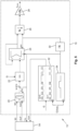
- FIG 5 shows an optimized feedback loop 19 used in the digital signal processor 15 of Figure 1 according to an embodiment to prevent the abrupt changes of the output voltage during the transition phases from the low to the high gain driving modes and vice versa.
- the feedback loop 19 comprises a deserializer 20, a register shifter 22, an accumulator 24, a decimator filter 26 and a division element 28.
- the deserializer 20 is arranged to receive serial data SD from the ADC 46 as an input.
- the serial data SD are transmitted one bit at a time in a serial manner and synchronized on the clock CLK". These bits are parallelized to create a single value encoded on M bits.
- the register shifter 22 is used for changing the value if the current measurement has been performed with a gain different from the low gain in the analog front-end 44 to ensure that the values accumulated in the accumulator 24 are coherent and in the same range.
- the register shifter 22 is therefore controlled by an input signal G.
- G When G is in "one" state, the register shifter 22 is inactive, whereas when G is in "zero” state, the register shifter 22 shifts the bits in the register by one or more positions to the right so that the value is coherent with the current measurements. Shifting one bit to the right is equivalent to dividing the value (encoded in binary format) by two. This is why the ratio between the high gain mode and the low gain mode is typically designed to be a power of two, and the same exponent is used as the number of positions to shift the register in the shifter 22.
- Oversampling technique is used to increase the smoothness during the transition phases between the low and high gain driving modes and vice versa so as to suppress, or at least reduce, torque and speed ripples that occur during these transition phases as shown in Figure 4 .
- the accumulator 24 is arranged to add up different samples of currents measured by the current sensor 42.
- the decimator filter 26 is used for downsampling the current samples (keeping only every Nth sample), and the accumulator 24 is reset at this moment.
- a reset module 30 is foreseen to count samples and send a single pulse when the number N is reached. This pulse is used both by the decimator filter 26 to latch the current value of the output of the accumulator, and by the accumulator 24 to reset its value to zero.
- the reset module 30 is set up to count fifty samples and generate the pulse signal (SUM_Ready) for the accumulator in such a way that it adds up 50 current measurement samples and the decimator filter 26 latches the sum upon completion of the addition of the 50 measurement samples.
- the decimator filter 26 transmits the accumulated value to the division element 28 for outputting a moving average of the current measurement for each oversampled measurement made of 50 current measurement samples.
- the clock generator 32 of the digital processing unit is arranged to generate a first or a second clock signal CLK as a function of the selected gain G which is determined based on the previous current measurement.
- the control signal generator 34 is arranged to generate the control signal I CS so as to initiate an analog to digital conversion in the ADC and select the gain of the analog front-end 44 as previously described in relation to Figures 2 , 3a and 3b .
- the first and second clock signal CLK and control signal I CS are derived from a main cock CLK main generated by the digital processing unit 15.
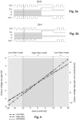
- Figures 6a shows a smoother variation of the output voltage from the low to the high gain driving modes during a first transition phase when the current changes from -10[A] to -5[A], as well as a smoother variation of the output voltage from the high to the low gain driving modes during a second transition phase when the current changes from 5[A] to 10[A] when using the feedback loop of Figure 5 .
- the number of ADC samples that are in low or high gain driving mode depends linearly on the previous current measurement as shown in Figure 6b . In this way it is possible to smooth out the transition and to avoid abrupt changes.
- each current measurement sample having a value ranging from -20[A] to -10[A] and from 10[A] to 20[A] has been performed when the analog front-end 44 was set to a low gain driving mode while each current measurement sample having a value ranging from -5[A] to +5[A] has been performed when the analog front-end 44 was set to a high gain driving mode.
- a certain percentage of current measurement samples have been performed in the low gain driving mode, while the rest of the current measurement samples have been performed in the high gain driving mode to add up to 100%.
- the percentage of the current measurement samples made in the low gain driving mode is low at the very beginning of this second transition phase and linearly increased such that around 20%, 40%, 60% and 80% of the current measurement samples are performed in the low gain driving mode while the respective remaining 80%, 60%, 40% and 20% of the current measurement samples are performed in the high gain driving mode for a current of around +6[A], +7[A], +8[A] and +9[A] respectively.
- the order in which the current measurement samples are performed in the first and second high gain driving mode does not impact the output of the control circuit 10.
- the current measurements samples that made up the 60% of samples taken in the low gain driving mode can be added together by the accumulator 24 in a row and the 40% of samples taken in the low gain driving mode can be added together thereafter or they can be mixed together without any predefined order considering that the sequence of order of the low and high driving modes does not have any effect on the moving average of the current measurement calculated by the division element 28.
- FIGs 7a to 7c show three different time diagrams for different operating conditions.
- each oversampled measurement is made of 50 ADC samples S0, S1, S2 Colour in the high gain driving mode, that is to say, in the particular case shown in Figures 6a and 6b , when the current load measured by the current sensor is in the range between -5[A] and +5[A].
- the amplifier noise is minimised, but only low currents can be measured (up to ⁇ 5 [A] in the example above).
- Figure 7b shows the timing diagram for the low gain driving mode.
- the gain never changes and the control signal G is set to the "one" state. This is the gain driving mode used when the current is inferior to -10[A] or exceeds +10[A].
- Figure 7c shows the timing diagram during the first or second transition phases of Figure 6b during which 50% of the current measurement samples are performed in the low gain driving mode and 50% of the current measurement samples are performed in the high gain driving mode for a current of -7.5[A] or +7.5[A].
- the current measurement samples are performed in the low and high gain driving modes in an alternate fashion.
- control circuit 10 may be adapted to control a single-phase or multiple phase AC motor, for instance a three-phase AC motor.
- control circuit may comprise three feedback loops as shown in Figures 1 and 5 for adjusting the current in each phase of the electric motor.
Landscapes
- Engineering & Computer Science (AREA)
- Power Engineering (AREA)
- Theoretical Computer Science (AREA)
- Physics & Mathematics (AREA)
- General Physics & Mathematics (AREA)
- Control Of Electric Motors In General (AREA)
Description
- The present invention relates to the field of electric motors and more particularly to a control circuit for an electric motor and a motor comprising such control circuit. The present invention further relates to a method for controlling the control circuit to achieve precise and accurate driving of electric motors.
- Electric motors used in various industrial installations are often controlled to achieve a target position. In this context, a feedback loop is used to modify the actual position of a moving part of the motor such that it corresponds to the target position. The difference between the actual position and the target position is processed by an electronic control unit, which determines a target supply current. The control unit of the motor is therefore adapted to supply the motor (each of its phases) in such a way as to generate a supply current corresponding to the target supply current to achieve high precision positioning of the moving part of the motor.
-
US8860354B2 discloses a control circuit for an electric motor, which is configured to generate via a first digital-to-analog converter, a control signal for driving the electric motor. The control circuit comprises a low-voltage zone and a high-voltage zone. The low-voltage zone comprises a control unit while the high-voltage zone comprises a current sensor for measuring the current supply to the electric motor and an analog-to-digital converter (ADC) to convert the analog signal into a corresponding digital signal which is sent to the control unit. A galvanic separating element is provided between the low and high-voltage zones for security reasons. - In order to achieve the required performance, the noise level on the output current Ioutput is crucial and is usually expressed in µArms. The noise level is directly linked to the current measurement's least significant bit (LSB) resolution. The smaller the LSB resolution, the better is the noise. The LSB resolution may be reduced in three different ways:
- the number of bits of the ADC can be increased. This has an immediate impact on the LSB resolution but impacts negatively the overall cost,
- a fast ADC with a limited number of bits may be used and an average from multiple current measurement samples can be calculated. This is equivalent to increasing the number of bits of the ADC, with the advantage that fast low-resolution ADC are usually cheaper than slow high-resolution ones. The gain in resolutions comes at expense of a bigger lag in the feedback loop, limiting again the dynamic performances of the driven motor, or
- the current sensor maximum current level can be reduced, thereby having an immediate positive impact on the LSB resolution. Reducing the sensor maximum current level has however a negative impact on the dynamic performances (e.g. acceleration, speed, torque) of the driven motor because large currents cannot be measured.
- However, large currents are not required through the whole operating range of the motor. When the motor is at standstill or running at constant speed, the current intensities are significantly smaller than the maximum drive current usually required during acceleration phases of the motor. Different driving modes may therefore be implemented according to the operating range of the motor.
-
US9383734 -
US6057664 discloses a motor driving control apparatus and a motor driving method. - USJP5556353 discloses a motor control detection IC and a motor control device using the same.
- An aim of the present invention is to provide an alternative control circuit, for driving an electric motor, which optimizes the current feedback as a function of the operating range of the electric motor.
- Another aim of the present invention is to provide a control circuit with high and low voltage subcircuit separated by a galvanic isolation and adapted to use an isolator with a limited number of channels to pass control data across the galvanic isolation barrier for selecting a low or high gain driving modes.
- Using an isolator with limited number of channels has the advantage to be cost-effective and compact.
- The invention is defined in the
independent apparatus claim 1 and the independent method claim 8. The preferred embodiments are defined in the dependent claims. - This aim is achieved by a control circuit for an electric motor comprising at least one phase. The control circuit comprises a low voltage subcircuit, a high voltage subcircuit and an isolation barrier between the low voltage and high voltage subcircuits. The low voltage subcircuit comprises a current controller adapted to generate a driving signal, and a feedback loop whose output is fed back to the input of the current controller. The high voltage subcircuit comprises a power bridge to output a current for driving the at least one phase of the motor, a current sensor for measuring the current in the at least one phase, an analog front-end and an analog-to-digital converter (ADC). The isolation barrier comprises an isolator adapted to pass the output signal of the ADC across the isolation barrier from the high voltage subcircuit to the low voltage subcircuit. The analog front-end is adapted to apply a first gain or a second gain that is higher than the first gain as a function of the current in the at least one phase measured by the current sensor.
- The isolator comprises a first and a second channel to pass respectively a clock signal and a control signal from the low voltage subcircuit to the high voltage subcircuit in order to select the first or second gain of the analog front-end. The isolator comprises a third and a fourth channel to pass respectively the output data of the ADC and a replica of the clock signal from the high voltage subcircuit to the low voltage subcircuit.
- In an embodiment, the high voltage subcircuit further comprises a D flip-flop. The clock input of the D flip-flop is arranged to receive the control signal and the input of the D flip-flop is arranged to receive the clock signal. The output of the D flip-flop is used for selection of either first or second gain of the analog front-end as a function of the clock signal.
- In an embodiment, the high voltage subcircuit further comprises a multiplexer comprising two data inputs and a selector input, wherein one of the two data inputs is arranged to receive the clock signal, the other of the two data inputs is arranged to receive the output of the D flip-flop. The selector input is arranged to receive the control signal such that either the selected gain or the replica of the clock signal may be passed via the fourth channel of the isolator based on the state of the control signal.
- In an embodiment, the feedback loop of the low voltage subcircuit comprises a deserializer arranged to receive serial data from the ADC, representing the current value measured by the current sensor, as an input to convert the serial data into a single value encoded on M bits. The feedback loop also comprises a register shifter for changing the value of said M bits if the selected first or second gain differs from the gain applied to said current value.
- In an embodiment, the feedback loop further comprises an accumulator arranged to add up different samples of currents measured by the current sensor, a decimator filter for sampling N current samples and a division element for outputting a moving average of the current measurements.
- In an embodiment, the feedback loop further comprises a clock generator arranged to generate a first or a second clock signal as a function of the selected first or second gain. The selection of the first or second gain is based on the current measured by the current sensor.
- In an embodiment, the clock generator is arranged to adapt the first and second clock signals, when the current measured by the current sensor is between a first and a second current thresholds, such that the moving average of the current measurement outputted by the division element is made up of current samples measured with the first gain and current samples measured with the second gain during a transition phase from a low to a high gain driving mode or from a high to a low gain driving mode.
- Another aspect of the invention relates to an electric motor comprising the control circuit as described above.
- A further aspect of the invention relates to a method for controlling the control circuit for an electric motor, comprising the steps of
- measuring the current flowing in the at least one phase of the electric motor, and
- controlling the front analog front-end such that:
- i) its gain corresponds to the first gain as long as the current measured is below a first current threshold value,
- ii) its gain corresponds to the second gain as long as the current measured is above a second current threshold value,
- iii) its gain corresponds to the first and second gains for respectively a first and a second set of current measurement samples taken during a transition phase extending from the first current threshold value to the second current threshold value.
- In an embodiment, the transition phase is divided into N sub-transition phases. A first sub-transition phase is the sub-transition phase just above the first current threshold value. A last sub-transition phase is the sub-transition phase just below the second current threshold value. At least 90% of 100/N %, and preferably around 100/N % of the current measurement samples are taken during the first sub-transition phase with the second gain while the rest of the current measurement samples are taken during the first sub-transition phase with the first gain. At least 90% of 100/N %, and preferably around 100/N % of the current measurement samples are taken during the last sub-transition phase with the first gain while the rest of the current measurement samples are taken during the last sub-transition phase with the second gain.
- The invention will be better understood with the aid of the description of several embodiments given by way of examples and illustrated by the figures, in which:
-
Figure 1 shows a simplified block diagram of the control circuit for driving an electric motor according to an embodiment; -
Figure 2 shows an electronic circuit diagram of a gain selector according to an embodiment; -
Figures 3a and 3b are serial data frames for selecting a gain of a first and a second gain driving mode respectively, -
Figure 4 is a graph showing abrupt changes of the output voltage at the transition from a low gain to a high gain driving mode and at the transition from the high gain to the low gain driving modes; -
Figure 5 shows a feedback loop used in the digital signal processor ofFigure 1 according to an embodiment to prevent the abrupt changes of the output voltage at the transition phases from the low to the high gain driving modes and vice versa shown inFigure 4 ; -
Figure 6a is a graph showing a first smoother transition of the output voltage from the low to the high gain driving modes during a first transition phase when the current changes from -10A to -5A, and a second smoother transition of the output voltage from the high to the low gain driving modes during a second transition phase when the current changes from 5A to 10A when using the feedback loop ofFigure 5 ; -
Figure 6b is a graph showing ADC samples with low and high gain modes percentages during respective first and second transition phases; -
Figure 7a is a time diagram corresponding to the high gain driving mode; -
Figure 7b is a time diagram corresponding to the low gain driving mode, and -
Figure 7c shows a time diagram corresponding to a transition mode in which 50% of current measurement samples are taken during the low gain driving mode and 50% of current measurement samples are taken during the high gain driving mode. -
Figure 1 shows a simplified block diagram of acontrol circuit 10 for an electric motor having at least one phase according to an embodiment. Thecontrol circuit 10 comprises alow voltage subcircuit 12a, ahigh voltage subcircuit 12b and anisolation barrier 50 between the low voltage andhigh voltage subcircuits low voltage subcircuit 12a has adigital signal processor 15 comprising acurrent controller 16. The digital signal processor can optionally be replaced by a programmable logic element such as a field programmable gate array (FPGA). Thecurrent controller 16 may comprise for example aPI controller 17 and acomparator 18 to output a PWM signal. ThePI controller 17 is adapted to correct an error value based on a reference signal Iref and a feedback measurement value. A PID controller may however be used instead of the PI controller in an alternative embodiment. - The
high voltage subcircuit 12b comprises apower bridge 40 to control the electric motor, acurrent sensor 42 for measuring the current flowing in the at least one phase of the electric motor when operating, an analog-front-end 44 for signal conditioning of the current signal to exploit the full input range of an analog-digital converter (ADC) 46. Thecurrent sensor 42 is preferably a shunt resistance Rsh (Figure 2 ). The current builds up a voltage across the shunt resistance Rsh. This voltage is then amplified by the analog front-end 44 and digitally converted by theADC 46. - The
isolation barrier 50 is an essential element for safety reasons. The isolation barrier comprises agate driver 52 to produce a high-current drive input for the gate of the transistors of thepower bridge 40 and anisolator 54 so that the serial data outputted by theADC 46 may cross theisolation barrier 50. Thegate driver 52 andisolator 54 may comprise for example transformers, optocouplers or capacitive couplers to create the isolation barrier between the low andhigh voltage subcircuits - With reference to
Figure 2 , theisolator 54 comprises only four channels which has the advantage of being cost effective and having a reduced footprint in comparison with other isolators with higher numbers of channels. Two of the four channels are used to pass a clock signal CLK and a control signal ICS from the low to thehigh voltage subcircuits clock generator 32 and acontrol signal generator 34 of thedigital signal processor 15 as shown inFigure 5 . - The other two channels are used to pass a serial data signal SD outputted by the
ADC 46 and a clock signal CLK", which is a replica of the above clock signal CLK, back to thelow voltage circuit 12a to synchronize the clock signal in the low voltage side of the control circuit with the serial data outputted by theADC 46 in order to avoid the risk of desynchronisation between the data and the clock due to isolation barrier delays. - It must be noted that when the motor is at standstill or operating at constant speed, the current levels are significantly smaller than current usually required during acceleration phases of the motor. In addition, a low noise level on the current outputted by the
control circuit 10 is required when the motor is at standstill. Thecontrol circuit 10 is therefore adapted to switch the gain of the analog front-end 44 such that the motor is driven either in a low or high gain driving mode as a function of the current measured by thecurrent sensor 42. - The
control circuit 10 is configured, on the one hand, to set the analog front-end 44 in a high gain driving mode when current flowing in one phase of the electric motor measured by thecurrent sensor 42 is below a first current threshold in order to reduce the LSB size and, on the other hand, to set the analog front-end 44 in a low gain driving mode, when the current flowing in said one phase measured by the current sensor exceeds a second current threshold, in order to reach the maximum current level to achieve optimal dynamic performances. - Therefore, a high or low gain information coded on one bit (G=1 or 0) must also be transferred across the isolation barrier via the
isolator 54, despite the constraint in terms of limited channels, in order to set the analog front-end 44 in the low or high gain driving mode. - The electronic circuit diagram, illustrated in
Figure 2 , is adapted to pass such high or low gain information. To this end, thehigh voltage subcircuit 12b of thecontrol circuit 10 ofFigure 1 further comprises a D flip-flop 47 and amultiplexer 48 arranged to control the gain of the analog front-end 44 as a function of current measurement samples. More particularly, the clock signal CLK and the control signal ICS generated by respectively aclock generator 32 and acontrol signal generator 34 of thedigital signal processor 15 as shown inFigure 5 , may cross theisolation barrier 50 from the low volage side to the high voltage side of thecontrol circuit 10 via respectively the first and the second channel of theisolator 54. - The serial data SD outputted by the
ADC 46 may cross theisolation barrier 50 from the high voltage side to the low voltage side of thecontrol circuit 10 via the third channel. The clock input of the D flip-flop 47 is arranged to receive the control signal ICS and the input of the D flip-flop 47 is arranged to receive the clock signal CLK. The inverted output of the D flip-flop which has been named G, represented inFigures 3a and 3b , is used for selection of a low gain or a high gain of the analog front-end 44 as a function of the current measured by thecurrent sensor 42. In the electronic circuit diagram illustrated inFigure 2 , the inverted output of the D flip-flop has been used for the selection of gain, but the non-inverted output could also have been used depending on the circuit design. - In other words, the signals are swapped, in such a way that the control signal ICS is used as the clock input of the D flip-flop, whereas the clock is used as the input to be sampled. Typically, the output of the D flip-flop is in a "zero" state (G=0) to set the analog front-
end 44 to the high gain driving mode for low currents and where position stability is crucial, whereas the output of the D flip-flop is in a "one" state (G=1) to set the analog front-end 44 to the low gain driving mode for dynamic acceleration phases of the electric motor. - The electronic circuit diagram of
Figure 2 further comprises amultiplexer 48 comprising two inputs and a selector input SEL. One input of themultiplexer 48 is arranged to receive the clock signal CLK while the other input of themultiplexer 48 is arranged to receive the output of the D flip-flop 47. The selector input SEL is arranged to receive the control signal ICS such that either the selected gain G or the replicated clock signal CLK" may pass via the fourth channel of the isolator 54 from the high voltage side to the low voltage side of the control circuit based on the state of the control signal ICS. Typically, the selected gain G will pass through the multiplexer when the control signal ICS is in high state (ICS=1), and the replicated clock signal CLK" will pass through the multiplexer when the control signal ICS is in low state (ICS=0). This allows conditioning of the signal in thelow voltage subcircuit 12a as a function of the selected gain G, as described in detail subsequently with reference toFigure 5 . - The low and high gain driving modes are used as a function of the intensity of load current of the electric motor to exploit the benefits of both driving modes as already mentioned above. For example, let us assume that a ratio of two has been foreseen by design between the high gain mode and the low gain mode. Indeed, any power of two is optimal to be able to use a
simple register shifter 22 in the subsequent signal processing. However, in practice, an exact gain of two is never obtained due to the tolerances on the values of electronic components. Therefore, in the current range around the threshold it is necessary to make a smooth transition from the low gain driving mode to the high gain driving mode and vice versa to prevent abrupt changes, as shown inFigure 4 , resulting in torque and speed ripples. -
Figure 5 shows an optimizedfeedback loop 19 used in thedigital signal processor 15 ofFigure 1 according to an embodiment to prevent the abrupt changes of the output voltage during the transition phases from the low to the high gain driving modes and vice versa. Thefeedback loop 19 comprises adeserializer 20, aregister shifter 22, anaccumulator 24, adecimator filter 26 and adivision element 28. - The
deserializer 20 is arranged to receive serial data SD from theADC 46 as an input. The serial data SD are transmitted one bit at a time in a serial manner and synchronized on the clock CLK". These bits are parallelized to create a single value encoded on M bits. - The
register shifter 22 is used for changing the value if the current measurement has been performed with a gain different from the low gain in the analog front-end 44 to ensure that the values accumulated in theaccumulator 24 are coherent and in the same range. Theregister shifter 22 is therefore controlled by an input signal G. When G is in "one" state, theregister shifter 22 is inactive, whereas when G is in "zero" state, theregister shifter 22 shifts the bits in the register by one or more positions to the right so that the value is coherent with the current measurements. Shifting one bit to the right is equivalent to dividing the value (encoded in binary format) by two. This is why the ratio between the high gain mode and the low gain mode is typically designed to be a power of two, and the same exponent is used as the number of positions to shift the register in theshifter 22. - Oversampling technique is used to increase the smoothness during the transition phases between the low and high gain driving modes and vice versa so as to suppress, or at least reduce, torque and speed ripples that occur during these transition phases as shown in
Figure 4 . Accordingly, theaccumulator 24 is arranged to add up different samples of currents measured by thecurrent sensor 42. Thedecimator filter 26 is used for downsampling the current samples (keeping only every Nth sample), and theaccumulator 24 is reset at this moment. Areset module 30 is foreseen to count samples and send a single pulse when the number N is reached. This pulse is used both by thedecimator filter 26 to latch the current value of the output of the accumulator, and by theaccumulator 24 to reset its value to zero. - In the exemplary embodiment shown in
Figures 7a to 7c , thereset module 30 is set up to count fifty samples and generate the pulse signal (SUM_Ready) for the accumulator in such a way that it adds up 50 current measurement samples and thedecimator filter 26 latches the sum upon completion of the addition of the 50 measurement samples. Thedecimator filter 26 transmits the accumulated value to thedivision element 28 for outputting a moving average of the current measurement for each oversampled measurement made of 50 current measurement samples. - The
clock generator 32 of the digital processing unit, as shown inFigure 5 , is arranged to generate a first or a second clock signal CLK as a function of the selected gain G which is determined based on the previous current measurement. Thecontrol signal generator 34 is arranged to generate the control signal ICS so as to initiate an analog to digital conversion in the ADC and select the gain of the analog front-end 44 as previously described in relation toFigures 2 ,3a and 3b . The first and second clock signal CLK and control signal ICS are derived from a main cock CLKmain generated by thedigital processing unit 15. -
Figures 6a shows a smoother variation of the output voltage from the low to the high gain driving modes during a first transition phase when the current changes from -10[A] to -5[A], as well as a smoother variation of the output voltage from the high to the low gain driving modes during a second transition phase when the current changes from 5[A] to 10[A] when using the feedback loop ofFigure 5 . During the first and second transition phases, the number of ADC samples that are in low or high gain driving mode depends linearly on the previous current measurement as shown inFigure 6b . In this way it is possible to smooth out the transition and to avoid abrupt changes. - More particularly, as illustrated in
Figure 6b , each current measurement sample having a value ranging from -20[A] to -10[A] and from 10[A] to 20[A] has been performed when the analog front-end 44 was set to a low gain driving mode while each current measurement sample having a value ranging from -5[A] to +5[A] has been performed when the analog front-end 44 was set to a high gain driving mode. During the first and second transition phases ranging from -10[A] to -5[A] and from 5[A] to 10[A] respectively, a certain percentage of current measurement samples have been performed in the low gain driving mode, while the rest of the current measurement samples have been performed in the high gain driving mode to add up to 100%. - One would indeed see from the first transition phase of
Figure 6b that the percentage of the current measurement samples made in the low gain driving mode is high at the very beginning of this first transition phase and linearly decreased such that around 80%, 60%, 40% and 20% of the current measurement samples are performed in the low gain driving mode while the respective remaining 20%, 40%, 60% and 80% of the current measurement samples are performed in the high gain driving mode for a current of around -9[A], -8[A], -7[A] and -6[A] respectively. - Likewise, one would see from the second transition phase of
Figure 6b that the percentage of the current measurement samples made in the low gain driving mode is low at the very beginning of this second transition phase and linearly increased such that around 20%, 40%, 60% and 80% of the current measurement samples are performed in the low gain driving mode while the respective remaining 80%, 60%, 40% and 20% of the current measurement samples are performed in the high gain driving mode for a current of around +6[A], +7[A], +8[A] and +9[A] respectively. - The order in which the current measurement samples are performed in the first and second high gain driving mode does not impact the output of the
control circuit 10. For example, for current measurement samples of around +7[A], the current measurements samples that made up the 60% of samples taken in the low gain driving mode can be added together by theaccumulator 24 in a row and the 40% of samples taken in the low gain driving mode can be added together thereafter or they can be mixed together without any predefined order considering that the sequence of order of the low and high driving modes does not have any effect on the moving average of the current measurement calculated by thedivision element 28. -
Figures 7a to 7c show three different time diagrams for different operating conditions. InFigure 7a , each oversampled measurement is made of 50 ADC samples S0, S1, S2 [...] in the high gain driving mode, that is to say, in the particular case shown inFigures 6a and 6b , when the current load measured by the current sensor is in the range between -5[A] and +5[A]. When working in this region, the amplifier noise is minimised, but only low currents can be measured (up to ±5 [A] in the example above). -
Figure 7b shows the timing diagram for the low gain driving mode. The gain never changes and the control signal G is set to the "one" state. This is the gain driving mode used when the current is inferior to -10[A] or exceeds +10[A]. -
Figure 7c shows the timing diagram during the first or second transition phases ofFigure 6b during which 50% of the current measurement samples are performed in the low gain driving mode and 50% of the current measurement samples are performed in the high gain driving mode for a current of -7.5[A] or +7.5[A]. In this particular example, the current measurement samples are performed in the low and high gain driving modes in an alternate fashion. - Various modifications and variations to the described embodiments of the invention will be apparent to those skilled in the art without departing from the scope of the invention as defined in the appended claims. For example, the
control circuit 10 may be adapted to control a single-phase or multiple phase AC motor, for instance a three-phase AC motor. In the latter case, the control circuit may comprise three feedback loops as shown inFigures 1 and5 for adjusting the current in each phase of the electric motor. -
Control circuit 10 -
Low voltage subcircuit 12a-
Digital signal processor 15-
Current controller 16-
PI controller 17 -
Comparator 18
-
-
Control loop 19-
Deserializer 20 -
Register shifter 22 -
Accumulator 24 -
Decimator filter 26 -
Division element 28 -
Reset module 30 -
Clock generator 32 -
Control signal generator 34
-
-
-
-
High voltage subcircuit 12b-
Power bridge 40 -
Current sensor 42 - Analog Front-
End 44 -
ADC converter 46 - Flip-
Flop 47 -
Multiplexer 48
-
-
Isolation barrier 50-
Gate driver 52 -
Isolator 54
-
- Control signal ICS
- Gain selector signal G
- Serial data SD
- Shunt resistance Rsh
- Clock signal CLK
- Clock signal replica CLK"
Claims (8)
- A control circuit (10) for an electric motor comprising at least one phase, the control circuit (10) comprising a low voltage subcircuit (12a), a high voltage subcircuit (12b) and an isolation barrier (50) between the low voltage and high voltage subcircuits (12a, 12b), the low voltage subcircuit (12a) comprising a current controller (16) adapted to generate a driving signal, and a feedback loop (19) whose output is fed back to the input of the current controller (16), the high voltage subcircuit (12b) comprising a power bridge (40) to output a current for driving the at least one phase of the motor, a current sensor (42) for measuring the current in said at least one phase, an analog front-end (44) for signal conditioning of the current signal and an analog-to-digital converter-ADC (46) to digitally convert the conditioned signal, the isolation barrier (50) comprising an isolator (54) adapted to pass the output signal of the ADC (46) across the isolation barrier (50) from the high voltage subcircuit (12b) to the low voltage subcircuit (12c), wherein the isolator (54) comprises a first and a second channel to pass respectively a clock signal (CLK) and a control signal (ICS) from the low voltage subcircuit (12a) to the high voltage subcircuit (12b), the isolator (54) comprising a third channel to pass the output of the ADC (46) from the high voltage subcircuit (12a) to the low voltage subcircuit (12b)characterized in that the analog front-end (44) is adapted to apply a first gain or a second gain that is higher than the first gain as a function of the current in said at least one phase measured by the current sensor (42),wherein said clock signal (CLK) and control signal (ICS) are output to select said first or second gain (G) of the analog front-end (44), and wherein the isolator (54) comprises a fourth channel to pass a replica of the clock signal (CLK") from the high voltage subcircuit (12a) to the low voltage subcircuit (12b), the high voltage subcircuit (12a) further comprising a D flip-flop (47), and wherein the clock input of the D flip-flop (47) is arranged to receive the control signal (ICS) while the input of the D flip-flop (47) is arranged to receive said clock signal (CLK), the output of the D-flip-flop (47) being used for selection of said first or second gain of the analog front-end (44).
- The control circuit (10) according to claim 1, the high voltage subcircuit (12a) further comprising a multiplexer (48) comprising two inputs (0, 1) and a selector input (SEL), wherein one of the two inputs is arranged to receive the clock signal (CLK), the other of the two inputs is arranged to receive the output of the D-flip-flop (47) and the selector input (SEL) is arranged to receive the control signal (ICS) such that either the selected gain (G) or the replica of the clock signal (CLK") may be passed via the fourth channel of the isolator (54) based on the state of the control signal (ICS).
- The control circuit (10) according to any preceding claim, wherein the feedback loop (19) of the low voltage subcircuit (12b) comprises a deserializer (20) arranged to receive serial data (SD) from the ADC (46), representing the current value measured by the current sensor (42), as an input to convert the serial data (SD) into a single value encoded on M bits, and a register shifter (22) for changing the value of said M bits if the selected first or second gain (G) differs from the gain applied to said current value.
- The control circuit (10) according to the preceding claim, wherein said feedback loop (19) further comprises an accumulator (24) arranged to add up different samples of currents measured by the current sensor (42), a decimator filter (26) for sampling N current samples and a division element (28) for outputting a moving average of the current measurement.
- The control circuit (10) according to the preceding claim, wherein the feedback loop (19) further comprises a clock generator (32), said clock signal (CLK) is either a first or a second clock signal (CLK) generated by the clock generator (32) as a function of the selected first or second gain (G) which is based on the current measured by the current sensor (42).
- The control circuit (10) according to the preceding claim, wherein said clock generator (32) is arranged to adapt said first and second clock signals (CLK), when the current measured by the current sensor (42) is between a first and a second current threshold value, such that the moving average of the current measurement outputted by the division element (28) is made up of current samples measured with the first gain and current samples measured with the second gain during a transition phase from a low to a high gain driving mode or from a high to a low gain driving mode.
- Electric motor comprising a control circuit (10) according to any of the preceding claim.
- Method for controlling the control circuit (10) for an electric motor comprising the control circuit according to any of claims 1 to 5, comprising the steps of- measuring the current flowing in the at least one phase of the electric motor, and- controlling the front analog front-end (44) such that:i) its gain correspond to said first gain as long as the current measured is below a first current threshold value,ii) its gain correspond to said second gain as long as the current measured is above a second current threshold value,iii) its gain correspond to said first and second gain for respectively a first and a second set of current measurement samples taken during a transition phase extending from the first current threshold value to the second current threshold value, characterized in that said transition phase is divided into N sub-transition phases, the first sub-transition phase being the sub-transition phase just above said first current threshold value, the last sub-transition phase is the sub-transition phase just below said second current threshold value, wherein at least 90% of 100/N %, and preferably around 100/N % of the current measurement samples are taken during the first sub-transition phase with said second gain while the rest of the current measurement samples are taken during said first sub-transition phase with the first gain, and wherein at least 90% of 100/N %, and preferably around 100/N % of the current measurement samples are taken during the last sub-transition phase with said first gain while the rest of the current measurement samples are taken during said last sub-transition phase with the second gain.
Priority Applications (5)
| Application Number | Priority Date | Filing Date | Title |
|---|---|---|---|
| EP21193885.7A EP4142145B1 (en) | 2021-08-30 | 2021-08-30 | Control circuit for an electric motor and controlling method thereof |
| CN202210799887.XA CN115733398A (en) | 2021-08-30 | 2022-07-08 | Control circuit of motor and control method thereof |
| KR1020220093932A KR20230032889A (en) | 2021-08-30 | 2022-07-28 | Control circuit for an electric motor and controlling method thereof |
| US17/889,392 US12212260B2 (en) | 2021-08-30 | 2022-08-17 | Control circuit for an electric motor and controlling method thereof |
| JP2022131491A JP2023035919A (en) | 2021-08-30 | 2022-08-22 | Control circuit for electric motor and control method of the same |
Applications Claiming Priority (1)
| Application Number | Priority Date | Filing Date | Title |
|---|---|---|---|
| EP21193885.7A EP4142145B1 (en) | 2021-08-30 | 2021-08-30 | Control circuit for an electric motor and controlling method thereof |
Publications (2)
| Publication Number | Publication Date |
|---|---|
| EP4142145A1 EP4142145A1 (en) | 2023-03-01 |
| EP4142145B1 true EP4142145B1 (en) | 2025-01-22 |
Family
ID=77595305
Family Applications (1)
| Application Number | Title | Priority Date | Filing Date |
|---|---|---|---|
| EP21193885.7A Active EP4142145B1 (en) | 2021-08-30 | 2021-08-30 | Control circuit for an electric motor and controlling method thereof |
Country Status (5)
| Country | Link |
|---|---|
| US (1) | US12212260B2 (en) |
| EP (1) | EP4142145B1 (en) |
| JP (1) | JP2023035919A (en) |
| KR (1) | KR20230032889A (en) |
| CN (1) | CN115733398A (en) |
Families Citing this family (2)
| Publication number | Priority date | Publication date | Assignee | Title |
|---|---|---|---|---|
| US12149389B2 (en) * | 2023-01-18 | 2024-11-19 | Renesas Electronics America Inc. | Isolator with forward and return paths |
| CN120949845B (en) * | 2025-10-15 | 2025-12-23 | 武汉格蓝若精密技术有限公司 | Driving circuit and vibration reduction system |
Family Cites Families (12)
| Publication number | Priority date | Publication date | Assignee | Title |
|---|---|---|---|---|
| JPH0758638A (en) * | 1993-08-11 | 1995-03-03 | Yokogawa Electric Corp | A / D converter |
| JPH09229823A (en) * | 1996-02-21 | 1997-09-05 | Fujitsu Ten Ltd | Peak detection circuit for knocking detection, knock determination circuit and reset circuit |
| JP3421277B2 (en) * | 1998-08-26 | 2003-06-30 | 三菱電機株式会社 | Motor drive control device and motor drive control method |
| US6469461B1 (en) * | 1999-10-05 | 2002-10-22 | Denso Corporation | Motor control apparatus |
| AT500608B1 (en) * | 2004-07-14 | 2008-07-15 | Siemens Ag Oesterreich | METHOD FOR CONTROLLING A CLEARING DEVICE FOR A RESERVOIRING RECTIFIER BRIDGE |
| JP4962282B2 (en) * | 2007-11-20 | 2012-06-27 | 富士通株式会社 | Semiconductor device |
| KR101412826B1 (en) * | 2008-03-31 | 2014-06-27 | 미쓰비시덴키 가부시키가이샤 | Motor drive control apparatus |
| IL203642A (en) * | 2010-02-01 | 2014-01-30 | Yesaiahu Redler | Apparatus and method for optimizinmg current use during control of multiple motors and a projectile device containing the same |
| JP5556353B2 (en) * | 2010-05-07 | 2014-07-23 | パナソニック株式会社 | Motor current detector and motor control device |
| CH703739A2 (en) | 2010-08-31 | 2012-03-15 | Etel Sa | Control circuit of an electric motor with a servo-control of the supply current. |
| JP5850073B2 (en) * | 2014-03-18 | 2016-02-03 | ダイキン工業株式会社 | Power converter |
| IL235022A0 (en) | 2014-10-06 | 2015-02-01 | Vladimir Kogan | Motor servo-drive for high performance motion control |
-
2021
- 2021-08-30 EP EP21193885.7A patent/EP4142145B1/en active Active
-
2022
- 2022-07-08 CN CN202210799887.XA patent/CN115733398A/en active Pending
- 2022-07-28 KR KR1020220093932A patent/KR20230032889A/en active Pending
- 2022-08-17 US US17/889,392 patent/US12212260B2/en active Active
- 2022-08-22 JP JP2022131491A patent/JP2023035919A/en active Pending
Also Published As
| Publication number | Publication date |
|---|---|
| US20230062820A1 (en) | 2023-03-02 |
| US12212260B2 (en) | 2025-01-28 |
| JP2023035919A (en) | 2023-03-13 |
| EP4142145A1 (en) | 2023-03-01 |
| CN115733398A (en) | 2023-03-03 |
| KR20230032889A (en) | 2023-03-07 |
Similar Documents
| Publication | Publication Date | Title |
|---|---|---|
| US20230062820A1 (en) | Control circuit for an electric motor and controlling method thereof | |
| EP0401245B1 (en) | Digital to analogue converter | |
| US20040155807A1 (en) | Subranging analog to digital converter with multi-phase clock timing | |
| US9722625B2 (en) | Semiconductor device and semiconductor device operating method | |
| US6147632A (en) | Sampling frequency conversion apparatus and fractional frequency dividing apparatus for sampling frequency conversion | |
| US20040239546A1 (en) | A/d conversion method and apparatus | |
| EP3382898A1 (en) | Analog-to-digital converter circuit and method for analog-to digital conversion | |
| EP1588492B1 (en) | An analog-to-digital conversion arrangement, a method for analog-to-digital conversion and a signal processing system, in which the conversion arrangement is applied | |
| US8508310B2 (en) | Method and device for generating PWM signals | |
| US20100301823A1 (en) | Power supply unit and control circuit of power supply unit | |
| US6661364B2 (en) | Semiconductor device for inverter controlling | |
| EP2811654A2 (en) | Resolution-boosted sigma delta analog-to-digital converter | |
| US5229771A (en) | Analog to digital converter for converting multiple analog input signals to corresponding digital output signals during one conversion cycle | |
| EP1295399B1 (en) | Method and apparatus of producing a digital depiction of a signal | |
| JPH10327594A (en) | Motor control device | |
| KR20090071705A (en) | Analog-to-Digital Converter Using Reference Voltage Selection Circuit | |
| CN109495112A (en) | Analog-to-digital conversion method and delta-sigma modulator | |
| KR100391776B1 (en) | Controller using digital signals for multi-channel SQUID systems | |
| JP5067385B2 (en) | AD converter, current detector using AD converter, and digital servo controller using current detector | |
| JP3016094B2 (en) | Double integral type AD converter | |
| RU2017063C1 (en) | Device for conversion of multiple-phase periodical signal | |
| KR100260492B1 (en) | Servo control system | |
| JPH0879019A (en) | Gate pulse generator | |
| JP5661047B2 (en) | Digital controller for parallel PMOS transistor substrate | |
| SU839044A1 (en) | Analogue-digital conversion device |
Legal Events
| Date | Code | Title | Description |
|---|---|---|---|
| PUAI | Public reference made under article 153(3) epc to a published international application that has entered the european phase |
Free format text: ORIGINAL CODE: 0009012 |
|
| STAA | Information on the status of an ep patent application or granted ep patent |
Free format text: STATUS: THE APPLICATION HAS BEEN PUBLISHED |
|
| AK | Designated contracting states |
Kind code of ref document: A1 Designated state(s): AL AT BE BG CH CY CZ DE DK EE ES FI FR GB GR HR HU IE IS IT LI LT LU LV MC MK MT NL NO PL PT RO RS SE SI SK SM TR |
|
| STAA | Information on the status of an ep patent application or granted ep patent |
Free format text: STATUS: REQUEST FOR EXAMINATION WAS MADE |
|
| 17P | Request for examination filed |
Effective date: 20230829 |
|
| RBV | Designated contracting states (corrected) |
Designated state(s): AL AT BE BG CH CY CZ DE DK EE ES FI FR GB GR HR HU IE IS IT LI LT LU LV MC MK MT NL NO PL PT RO RS SE SI SK SM TR |
|
| GRAP | Despatch of communication of intention to grant a patent |
Free format text: ORIGINAL CODE: EPIDOSNIGR1 |
|
| STAA | Information on the status of an ep patent application or granted ep patent |
Free format text: STATUS: GRANT OF PATENT IS INTENDED |
|
| RIC1 | Information provided on ipc code assigned before grant |
Ipc: H02P 29/40 20160101AFI20240925BHEP |
|
| INTG | Intention to grant announced |
Effective date: 20241009 |
|
| GRAS | Grant fee paid |
Free format text: ORIGINAL CODE: EPIDOSNIGR3 |
|
| GRAA | (expected) grant |
Free format text: ORIGINAL CODE: 0009210 |
|
| STAA | Information on the status of an ep patent application or granted ep patent |
Free format text: STATUS: THE PATENT HAS BEEN GRANTED |
|
| AK | Designated contracting states |
Kind code of ref document: B1 Designated state(s): AL AT BE BG CH CY CZ DE DK EE ES FI FR GB GR HR HU IE IS IT LI LT LU LV MC MK MT NL NO PL PT RO RS SE SI SK SM TR |
|
| REG | Reference to a national code |
Ref country code: GB Ref legal event code: FG4D |
|
| REG | Reference to a national code |
Ref country code: CH Ref legal event code: EP |
|
| REG | Reference to a national code |
Ref country code: IE Ref legal event code: FG4D |
|
| REG | Reference to a national code |
Ref country code: DE Ref legal event code: R096 Ref document number: 602021025092 Country of ref document: DE |
|
| REG | Reference to a national code |
Ref country code: NL Ref legal event code: FP |
|
| PG25 | Lapsed in a contracting state [announced via postgrant information from national office to epo] |
Ref country code: RS Free format text: LAPSE BECAUSE OF FAILURE TO SUBMIT A TRANSLATION OF THE DESCRIPTION OR TO PAY THE FEE WITHIN THE PRESCRIBED TIME-LIMIT Effective date: 20250422 |
|
| PG25 | Lapsed in a contracting state [announced via postgrant information from national office to epo] |
Ref country code: FI Free format text: LAPSE BECAUSE OF FAILURE TO SUBMIT A TRANSLATION OF THE DESCRIPTION OR TO PAY THE FEE WITHIN THE PRESCRIBED TIME-LIMIT Effective date: 20250122 |
|
| PG25 | Lapsed in a contracting state [announced via postgrant information from national office to epo] |
Ref country code: PL Free format text: LAPSE BECAUSE OF FAILURE TO SUBMIT A TRANSLATION OF THE DESCRIPTION OR TO PAY THE FEE WITHIN THE PRESCRIBED TIME-LIMIT Effective date: 20250122 |
|
| PG25 | Lapsed in a contracting state [announced via postgrant information from national office to epo] |
Ref country code: ES Free format text: LAPSE BECAUSE OF FAILURE TO SUBMIT A TRANSLATION OF THE DESCRIPTION OR TO PAY THE FEE WITHIN THE PRESCRIBED TIME-LIMIT Effective date: 20250122 |
|
| REG | Reference to a national code |
Ref country code: LT Ref legal event code: MG9D |
|
| PG25 | Lapsed in a contracting state [announced via postgrant information from national office to epo] |
Ref country code: NO Free format text: LAPSE BECAUSE OF FAILURE TO SUBMIT A TRANSLATION OF THE DESCRIPTION OR TO PAY THE FEE WITHIN THE PRESCRIBED TIME-LIMIT Effective date: 20250422 Ref country code: IS Free format text: LAPSE BECAUSE OF FAILURE TO SUBMIT A TRANSLATION OF THE DESCRIPTION OR TO PAY THE FEE WITHIN THE PRESCRIBED TIME-LIMIT Effective date: 20250522 |
|
| PG25 | Lapsed in a contracting state [announced via postgrant information from national office to epo] |
Ref country code: HR Free format text: LAPSE BECAUSE OF FAILURE TO SUBMIT A TRANSLATION OF THE DESCRIPTION OR TO PAY THE FEE WITHIN THE PRESCRIBED TIME-LIMIT Effective date: 20250122 |
|
| PG25 | Lapsed in a contracting state [announced via postgrant information from national office to epo] |
Ref country code: PT Free format text: LAPSE BECAUSE OF FAILURE TO SUBMIT A TRANSLATION OF THE DESCRIPTION OR TO PAY THE FEE WITHIN THE PRESCRIBED TIME-LIMIT Effective date: 20250522 Ref country code: LV Free format text: LAPSE BECAUSE OF FAILURE TO SUBMIT A TRANSLATION OF THE DESCRIPTION OR TO PAY THE FEE WITHIN THE PRESCRIBED TIME-LIMIT Effective date: 20250122 |
|
| PG25 | Lapsed in a contracting state [announced via postgrant information from national office to epo] |
Ref country code: GR Free format text: LAPSE BECAUSE OF FAILURE TO SUBMIT A TRANSLATION OF THE DESCRIPTION OR TO PAY THE FEE WITHIN THE PRESCRIBED TIME-LIMIT Effective date: 20250423 Ref country code: BG Free format text: LAPSE BECAUSE OF FAILURE TO SUBMIT A TRANSLATION OF THE DESCRIPTION OR TO PAY THE FEE WITHIN THE PRESCRIBED TIME-LIMIT Effective date: 20250122 |
|
| PG25 | Lapsed in a contracting state [announced via postgrant information from national office to epo] |
Ref country code: SE Free format text: LAPSE BECAUSE OF FAILURE TO SUBMIT A TRANSLATION OF THE DESCRIPTION OR TO PAY THE FEE WITHIN THE PRESCRIBED TIME-LIMIT Effective date: 20250122 |
|
| PGFP | Annual fee paid to national office [announced via postgrant information from national office to epo] |
Ref country code: NL Payment date: 20250821 Year of fee payment: 5 |
|
| PG25 | Lapsed in a contracting state [announced via postgrant information from national office to epo] |
Ref country code: SM Free format text: LAPSE BECAUSE OF FAILURE TO SUBMIT A TRANSLATION OF THE DESCRIPTION OR TO PAY THE FEE WITHIN THE PRESCRIBED TIME-LIMIT Effective date: 20250122 |
|
| PG25 | Lapsed in a contracting state [announced via postgrant information from national office to epo] |
Ref country code: DK Free format text: LAPSE BECAUSE OF FAILURE TO SUBMIT A TRANSLATION OF THE DESCRIPTION OR TO PAY THE FEE WITHIN THE PRESCRIBED TIME-LIMIT Effective date: 20250122 |
|
| PGFP | Annual fee paid to national office [announced via postgrant information from national office to epo] |
Ref country code: DE Payment date: 20250820 Year of fee payment: 5 |
|
| PGFP | Annual fee paid to national office [announced via postgrant information from national office to epo] |
Ref country code: IT Payment date: 20250825 Year of fee payment: 5 |
|
| PGFP | Annual fee paid to national office [announced via postgrant information from national office to epo] |
Ref country code: AT Payment date: 20251020 Year of fee payment: 5 Ref country code: FR Payment date: 20250828 Year of fee payment: 5 |
|
| PGFP | Annual fee paid to national office [announced via postgrant information from national office to epo] |
Ref country code: CH Payment date: 20250901 Year of fee payment: 5 |
|
| PG25 | Lapsed in a contracting state [announced via postgrant information from national office to epo] |
Ref country code: CZ Free format text: LAPSE BECAUSE OF FAILURE TO SUBMIT A TRANSLATION OF THE DESCRIPTION OR TO PAY THE FEE WITHIN THE PRESCRIBED TIME-LIMIT Effective date: 20250122 Ref country code: EE Free format text: LAPSE BECAUSE OF FAILURE TO SUBMIT A TRANSLATION OF THE DESCRIPTION OR TO PAY THE FEE WITHIN THE PRESCRIBED TIME-LIMIT Effective date: 20250122 |
|
| REG | Reference to a national code |
Ref country code: DE Ref legal event code: R097 Ref document number: 602021025092 Country of ref document: DE |
|
| PG25 | Lapsed in a contracting state [announced via postgrant information from national office to epo] |
Ref country code: RO Free format text: LAPSE BECAUSE OF FAILURE TO SUBMIT A TRANSLATION OF THE DESCRIPTION OR TO PAY THE FEE WITHIN THE PRESCRIBED TIME-LIMIT Effective date: 20250122 |
|
| PG25 | Lapsed in a contracting state [announced via postgrant information from national office to epo] |
Ref country code: SK Free format text: LAPSE BECAUSE OF FAILURE TO SUBMIT A TRANSLATION OF THE DESCRIPTION OR TO PAY THE FEE WITHIN THE PRESCRIBED TIME-LIMIT Effective date: 20250122 |
|
| PLBE | No opposition filed within time limit |
Free format text: ORIGINAL CODE: 0009261 |
|
| STAA | Information on the status of an ep patent application or granted ep patent |
Free format text: STATUS: NO OPPOSITION FILED WITHIN TIME LIMIT |
|
| 26N | No opposition filed |
Effective date: 20251023 |
|
| REG | Reference to a national code |
Ref country code: AT Ref legal event code: UEP Ref document number: 1762220 Country of ref document: AT Kind code of ref document: T Effective date: 20250122 |
|
| PG25 | Lapsed in a contracting state [announced via postgrant information from national office to epo] |
Ref country code: MC Free format text: LAPSE BECAUSE OF FAILURE TO SUBMIT A TRANSLATION OF THE DESCRIPTION OR TO PAY THE FEE WITHIN THE PRESCRIBED TIME-LIMIT Effective date: 20250122 |
|
| PG25 | Lapsed in a contracting state [announced via postgrant information from national office to epo] |
Ref country code: LU Free format text: LAPSE BECAUSE OF NON-PAYMENT OF DUE FEES Effective date: 20250830 |
|
| GBPC | Gb: european patent ceased through non-payment of renewal fee |
Effective date: 20250830 |
|
| REG | Reference to a national code |
Ref country code: BE Ref legal event code: MM Effective date: 20250831 |
|
| PG25 | Lapsed in a contracting state [announced via postgrant information from national office to epo] |
Ref country code: LT Free format text: LAPSE BECAUSE OF FAILURE TO SUBMIT A TRANSLATION OF THE DESCRIPTION OR TO PAY THE FEE WITHIN THE PRESCRIBED TIME-LIMIT Effective date: 20250122 |
|
| PG25 | Lapsed in a contracting state [announced via postgrant information from national office to epo] |
Ref country code: GB Free format text: LAPSE BECAUSE OF NON-PAYMENT OF DUE FEES Effective date: 20250830 |
|
| PG25 | Lapsed in a contracting state [announced via postgrant information from national office to epo] |
Ref country code: BE Free format text: LAPSE BECAUSE OF NON-PAYMENT OF DUE FEES Effective date: 20250831 Ref country code: IE Free format text: LAPSE BECAUSE OF NON-PAYMENT OF DUE FEES Effective date: 20250830 |