EP4141963A1 - Semiconductor device and method for manufacturing semiconductor device - Google Patents
Semiconductor device and method for manufacturing semiconductor device Download PDFInfo
- Publication number
- EP4141963A1 EP4141963A1 EP21793142.7A EP21793142A EP4141963A1 EP 4141963 A1 EP4141963 A1 EP 4141963A1 EP 21793142 A EP21793142 A EP 21793142A EP 4141963 A1 EP4141963 A1 EP 4141963A1
- Authority
- EP
- European Patent Office
- Prior art keywords
- layer
- insulating film
- face
- metal layer
- trench
- Prior art date
- Legal status (The legal status is an assumption and is not a legal conclusion. Google has not performed a legal analysis and makes no representation as to the accuracy of the status listed.)
- Pending
Links
Images



Classifications
-
- H—ELECTRICITY
- H10—SEMICONDUCTOR DEVICES; ELECTRIC SOLID-STATE DEVICES NOT OTHERWISE PROVIDED FOR
- H10D—INORGANIC ELECTRIC SEMICONDUCTOR DEVICES
- H10D64/00—Electrodes of devices having potential barriers
- H10D64/60—Electrodes characterised by their materials
- H10D64/64—Electrodes comprising a Schottky barrier to a semiconductor
-
- H—ELECTRICITY
- H10—SEMICONDUCTOR DEVICES; ELECTRIC SOLID-STATE DEVICES NOT OTHERWISE PROVIDED FOR
- H10D—INORGANIC ELECTRIC SEMICONDUCTOR DEVICES
- H10D64/00—Electrodes of devices having potential barriers
- H10D64/01—Manufacture or treatment
-
- H—ELECTRICITY
- H10—SEMICONDUCTOR DEVICES; ELECTRIC SOLID-STATE DEVICES NOT OTHERWISE PROVIDED FOR
- H10D—INORGANIC ELECTRIC SEMICONDUCTOR DEVICES
- H10D8/00—Diodes
- H10D8/01—Manufacture or treatment
- H10D8/051—Manufacture or treatment of Schottky diodes
-
- H—ELECTRICITY
- H10—SEMICONDUCTOR DEVICES; ELECTRIC SOLID-STATE DEVICES NOT OTHERWISE PROVIDED FOR
- H10D—INORGANIC ELECTRIC SEMICONDUCTOR DEVICES
- H10D8/00—Diodes
- H10D8/60—Schottky-barrier diodes
-
- H—ELECTRICITY
- H10—SEMICONDUCTOR DEVICES; ELECTRIC SOLID-STATE DEVICES NOT OTHERWISE PROVIDED FOR
- H10D—INORGANIC ELECTRIC SEMICONDUCTOR DEVICES
- H10D8/00—Diodes
- H10D8/60—Schottky-barrier diodes
- H10D8/605—Schottky-barrier diodes of the trench conductor-insulator-semiconductor barrier type, e.g. trench MOS barrier Schottky rectifiers [TMBS]
Definitions
- the present disclosure relates to a semiconductor device and a method for manufacturing a semiconductor device.
- Japanese Unexamined Patent Application Publication No. 9-232597 describes manufacturing a semiconductor device having a Schottky junction.
- Manufacturing the semiconductor device involves: forming an insulating film on a surface of a semiconductor layer including a trench; embedding a conductor in the trench; exposing a region being part of the surface of the semiconductor layer and being adjacent to the trench by etching the insulating film away from the region; and forming a Schottky junction on the region in the surface of the semiconductor layer.
- a semiconductor device includes a semiconductor layer, an insulating film, a conductor, a silicide layer, and a metal layer.
- the semiconductor layer includes a trench. An inner surface of the trench is covered with the insulating film.
- the conductor is embedded in the trench covered with the insulating film.
- a Schottky junction is formed by the silicide layer and a region being part of a surface of the semiconductor layer and being adjacent to the trench.
- a region including an end face of the silicide layer and an upper end face of the insulating film is covered with the metal layer, with no gap between one part and another part of the metal layer on the region. The end face is located at elevations higher than the upper end face of the insulating film covering an inner wall surface of the trench.
- the metal layer and the silicide layer contain the same kind of metallic element.
- a method for manufacturing a semiconductor device includes: forming an insulating film on a surface of a semiconductor layer including a trench; embedding a conductor in the trench; exposing a region being part of a surface of the semiconductor layer and being adjacent to the trench by etching the insulating film away from the region; and forming a Schottky junction on the semiconductor layer.
- an upper end face of the insulating film covering an inner wall surface of the trench is lowered beyond the surface of the semiconductor layer.
- a metal layer is formed on the surface of the semiconductor layer, and a silicide layer is then formed by reaction between the metal layer and the semiconductor layer under heat treatment, with the Schottky junction being an interface between the silicide layer and the semiconductor layer.
- part of the metal layer is left unremoved to cover at least a region including an end face of the silicide layer and the upper end face of the insulating film with no gap between one part and another part of the metal layer on the region.
- a semiconductor device A1 includes a semiconductor layer 11, an insulating film 12, a conductor 13, a silicide layer 14, a metal layer 15, and an upper surface electrode 16.
- the semiconductor layer 11 includes a trench 10. An inner surface 10a of the trench 10 is covered with the insulating film 12.
- the conductor 13 is embedded in the trench 10 covered with the insulating film 12.
- the silicide layer 14 and a region being part of a semiconductor layer surface 11a and being adjacent to the trench 10 form a Schottky junction.
- the silicide layer 14 has an end face 14a, which is located at elevations higher than an upper end face 12a of the insulating film 12 covering an inner wall surface 10a1 of the trench 10.
- a region including the end face 14a of the silicide layer 14 and the upper end face 12a of the insulating film 12 is covered with the metal layer 15, with no gap between one part and another part of the metal layer 15 on the region.
- the conductor 13 may be polysilicon.
- the semiconductor layer 11 may be a silicon layer.
- the insulating film 12 may be a silicon oxide film.
- the upper surface electrode 16 may be made of aluminum.
- the silicide layer 14 is formed by the reaction between the semiconductor layer 11 and the metal layer 15.
- the silicide layer 14 is made of nickel silicide.
- a side face 11b of the semiconductor layer 11 is located at elevations higher than the upper end face 12a of the insulating film 12 and is covered with the metal layer 15.
- the semiconductor layer surface 11a is located at elevations higher than the upper end face 12a of the insulating film 12, with a Schottky junction being formed between the semiconductor layer surface 11a and the silicide layer 14.
- the semiconductor layer surface 11a and the side face 11b of the semiconductor layer 11 extend with no gap therebetween, and the side face 11b of the semiconductor layer 11 is located between the silicide layer 14 and the upper end face 12a of the insulating film 12.
- the side face 11b of the semiconductor layer 11 would be in direct contact with the upper surface electrode 16. During the application of a reverse voltage, a current would pass through the side face 11b. This would result in an increase in leakage current.
- the semiconductor device A1 can be averted by the semiconductor device A1 according to the present embodiment, in which the side face 11b of the semiconductor layer 11 is covered with the metal layer 15.
- the side face 11b of the semiconductor layer 11 is thus kept from direct contact with the upper surface electrode 16.
- the metallic element contained in the metal layer 15 is of the same kind as the metallic element contained in the silicide layer 14 forming the Schottky junction. That is, the metal forming the Schottky junction and the metal contained in the metal layer 15 are of the same kind, in which case the metal layer 15 provides a protective effect. More specifically, the metal layer 15 provides isolation between the side face 11b and the upper surface electrode 16 made of, for example, aluminum. During the application of a reverse voltage, a current is kept from passing through the side face 11b and the leakage current is kept low accordingly.
- the upper surface electrode 16 is in contact with an upper surface of the silicide layer 14 in such a manner that an interface between the upper surface electrode 16 and the upper surface of the silicide layer 14 is located in an opening of the metal layer 15.
- the silicide layer 14 forming the Schottky junction is electrically connected directly to the upper surface electrode 16.
- the following describes an example method for manufacturing the semiconductor device A1.
- the insulating film 12 is formed on the surface of the semiconductor layer 11 having the trench 10, and the conductor 13 is then embedded in the trench 10 (see FIG. 3 ). It is to be ensured that an upper surface 13a of the conductor 13 is located within the trench 10.
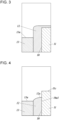
- the insulating film 12 is then etched away from a region being part of the semiconductor layer surface 11a and being adjacent to the trench 10 such that a surface of the semiconductor layer 11 is exposed to view (see FIG. 4 ).
- the surface of the semiconductor layer 11 is hereinafter referred to as a semiconductor layer surface 11c.
- the insulating film 12 is overetched to ensure that the semiconductor layer surface 11c is sufficiently exposed to view. That is, the upper end face 12a of the insulating film 12 covering the inner wall surface 10a1 of the trench 10 is etched deeper. More specifically, the upper end face 12a of the insulating film 12 covering the inner wall surface 10a1 of the trench 10 is lowered beyond the semiconductor layer surface 11c. As can be seen in FIG.
- the upper end face 12a is located at elevations lower than the semiconductor layer surface 11c. It is to be ensured that the insulating film on the semiconductor layer surface 11c is removed to a sufficient degree.
- the downward direction is herein regarded as meaning the direction in which the trench 10 in the surface of the semiconductor layer 11 is hollowed out, and the upward direction is herein regarded as meaning the reverse of it. These directions are not to be taken to mean the up-and-down direction (the direction of gravity) at the time of manufacturing of the semiconductor device or during periods of use of the semiconductor device.
- the metal layer 15 is formed on the semiconductor layer surface 11c, the upper end face 12a of the insulating film 12, and the upper surface 13a of the conductor 13 in such a manner that the metal layer 15 is in contact with the semiconductor layer surface 11c (see FIG. 5 ).
- the metal layer 15 and the semiconductor layer 11 are then subjected to heat treatment, where these layers react together to form the silicide layer 14 (see FIG. 6 ). Consequently, a Schottky junction is formed at an interface between the silicide layer 14 and the semiconductor layer 11 (the semiconductor layer surface 11a).
- the semiconductor device A1 obtained as above has the structure illustrated in FIGs. 1 and 2 .
- the semiconductor device A1 undergoes some other steps before it is in finished form.
- a region including the end face 14a of the silicide layer 14 and the upper end face 12a of the insulating film 12 is covered with the metal layer 15, with no gap between one part and another part of the metal layer 15 on the region. That is, an opening is formed by removing the metal layer 15 from the upper surface of the silicide layer 14 after the Schottky junction is formed while the region including the end face 14a of the silicide layer 14 and the upper end face 12a of the insulating film 12 is covered with the metal layer 15, with no gap between one part and another part of the metal layer 15 on the region.
- the side face 11b is included in the region concerned.
- the upper surface electrode 16 is then formed on the upper surface of the silicide layer 14 in such a manner that an interface between the upper surface electrode 16 and the upper surface of the silicide layer 14 is located in the opening.
- the metal layer 15 on the upper surface 13a of the conductor 13 is left unremoved. In some embodiments, the metal layer 15 on the upper surface 13a is removed.
- FIGs. 7 and 8 illustrate a semiconductor device B1 in Comparative Example.
- the semiconductor device B1 in Comparative Example differs from the semiconductor device A1 according to the present embodiment in the following respects only: (i) the semiconductor device B1 does not include the metal layer 15; and (ii) the upper surface electrode 16 of the semiconductor device B1 is in contact with the silicide layer 14, the upper end face 12a of the insulating film 12, and the upper surface 13a of the conductor 13.
- the method for manufacturing the semiconductor device B1 entails removing the entirety of the metal layer 15 before the step of forming an upper surface electrode.
- FIG. 9 illustrates the results of the voltage-current characteristics measurements under reverse bias.
- the reverse current was lower in the semiconductor device A1 according to the present embodiment than in the semiconductor device B1 in Comparative Example; that is, the semiconductor device A1 exhibited improved reverse characteristics.
- the semiconductor device offers the following advantages.
- the leakage current that flows through an edge portion of the Schottky junction during the application of a reverse voltage is kept low due to the protective effect provided by the metal layer 15.
- the insulating film on the semiconductor layer surface 11c is removed to a sufficient degree such that the semiconductor device exhibits favorable characteristics.
- the manufacturing method according to an embodiment of the present disclosure enables manufacturing of a semiconductor device that offers the following advantages. During the application of a reverse voltage, the leakage current is kept low due to the protective effect provided by the metal layer 15.
- the insulating film on the semiconductor layer surface 11c is removed to a sufficient degree such that the semiconductor device manufactured by the method exhibits favorable characteristics.
- the silicide layer 14 and the upper surface electrode 16 in the embodiment above are connected directly to each other in the opening formed in the metal layer 15 on the silicide layer 14.
- the silicide layer 14 and the upper surface electrode 16 may be electrically connected to each other with the metal layer 15 therebetween. This eliminates the need for the step of forming an opening in the metal layer 15.
- the side face 11b of the semiconductor layer 11 in the embodiment above is located between the silicide layer 14 and the upper end face 12a of the insulating film 12. In some embodiments, the side face 11b of the semiconductor layer 11 is not located between the silicide layer 14 and the upper end face 12a of the insulating film 12. As in the embodiment above, the leakage current may be kept low when a peripheral portion of the Schottky junction (a region including the end face 14a and the upper end face 12a) is covered with the metal layer 15.
- the upper end face 12a of the insulating film 12 and the semiconductor layer surface 11a are at the same depth, or the upper end face 12a is located slightly above the semiconductor layer surface 11a.
- a lower part of the end face 14a is covered with the insulating film 12, whereas an upper part of the end face 14a is not covered with the insulating film 12.
- the insulating film 12 fails to provide a sufficient covering and protection of the peripheral portion of the Schottky junction, the leakage current would increase.
- the leakage current may be kept low when the peripheral portion of the Schottky junction (the region including the end face 14a and the upper end face 12a) is covered with the metal layer 15.
- the present disclosure is not limited to an embodiment in which the side face 11b of the semiconductor layer 11 is located between the silicide layer 14 and the upper end face 12a of the insulating film 12. Nevertheless, the present invention is effective in keeping the leakage current low, particularly when the side face 11b of the semiconductor layer 11 is located between the silicide layer 14 and the upper end face 12a of the insulating film 12.
- the silicide layer 14 is formed by the reaction between the semiconductor layer 11 and the metal layer 15, and part of the metal layer 15 is left unremoved to provide the protective effect.
- the same or similar effects may be attained in some embodiments in which the metal layer 15 is entirely removed and is replaced with another metal layer 15 containing a metallic element that is of the same kind as the metallic element contained in the previously formed metal layer 15. Nevertheless, the embodiment above involves a fewer number of steps and thus provides good production efficiency.
- the embodiment above also makes effective use of the metal layer for forming the silicide layer 14. Eliminating wasted materials results in increased cost-effectiveness.
- the present disclosure is applicable to a semiconductor device and a method for manufacturing a semiconductor device.
Landscapes
- Electrodes Of Semiconductors (AREA)
- Engineering & Computer Science (AREA)
- Manufacturing & Machinery (AREA)
Abstract
Description
- The present disclosure relates to a semiconductor device and a method for manufacturing a semiconductor device.
-
Japanese Unexamined Patent Application Publication No. 9-232597 - According to an aspect of the present disclosure, a semiconductor device includes a semiconductor layer, an insulating film, a conductor, a silicide layer, and a metal layer. The semiconductor layer includes a trench. An inner surface of the trench is covered with the insulating film. The conductor is embedded in the trench covered with the insulating film. A Schottky junction is formed by the silicide layer and a region being part of a surface of the semiconductor layer and being adjacent to the trench. A region including an end face of the silicide layer and an upper end face of the insulating film is covered with the metal layer, with no gap between one part and another part of the metal layer on the region. The end face is located at elevations higher than the upper end face of the insulating film covering an inner wall surface of the trench. The metal layer and the silicide layer contain the same kind of metallic element.
- According to another aspect of the present disclosure, a method for manufacturing a semiconductor device includes: forming an insulating film on a surface of a semiconductor layer including a trench; embedding a conductor in the trench; exposing a region being part of a surface of the semiconductor layer and being adjacent to the trench by etching the insulating film away from the region; and forming a Schottky junction on the semiconductor layer. In the etching the insulating film, an upper end face of the insulating film covering an inner wall surface of the trench is lowered beyond the surface of the semiconductor layer. In the forming a Schottky junction, a metal layer is formed on the surface of the semiconductor layer, and a silicide layer is then formed by reaction between the metal layer and the semiconductor layer under heat treatment, with the Schottky junction being an interface between the silicide layer and the semiconductor layer. After the Schottky junction is formed, part of the metal layer is left unremoved to cover at least a region including an end face of the silicide layer and the upper end face of the insulating film with no gap between one part and another part of the metal layer on the region.
-
-
FIG. 1 is a schematic sectional view of a semiconductor device according to an embodiment of the present disclosure. -
FIG. 2 is a partial enlargement ofFIG. 1 . -
FIG. 3 is a schematic sectional view for explanation of a manufacturing process step involved in the production of the semiconductor device illustrated inFIG. 1 . -
FIG. 4 is a schematic sectional view for explanation of a manufacturing process step subsequent to the manufacturing process step that will be described with reference toFIG. 3 . -
FIG. 5 is a schematic sectional view for explanation of a manufacturing process step subsequent to the manufacturing process step that will be described with reference toFIG. 4 . -
FIG. 6 is a schematic sectional view for explanation of a manufacturing process step subsequent to the manufacturing process step that will be described with reference toFIG. 5 . -
FIG. 7 is a schematic sectional view of a semiconductor device in Comparative Example. -
FIG. 8 is a partial enlargement ofFIG. 7 . -
FIG. 9 illustrates the voltage-current characteristics measurements under reverse bias and graphically represents the characteristics in an illustrative example and the characteristics in Comparative Example. - Hereinafter, an embodiment of the present disclosure will be described with reference to the accompanying drawings.
- Referring to
FIGs. 1 and 2 , a semiconductor device A1 according to an embodiment of the present disclosure includes asemiconductor layer 11, aninsulating film 12, aconductor 13, asilicide layer 14, ametal layer 15, and anupper surface electrode 16. Thesemiconductor layer 11 includes atrench 10. Aninner surface 10a of thetrench 10 is covered with theinsulating film 12. Theconductor 13 is embedded in thetrench 10 covered with theinsulating film 12. Thesilicide layer 14 and a region being part of asemiconductor layer surface 11a and being adjacent to thetrench 10 form a Schottky junction. Thesilicide layer 14 has anend face 14a, which is located at elevations higher than anupper end face 12a of theinsulating film 12 covering an inner wall surface 10a1 of thetrench 10. A region including theend face 14a of thesilicide layer 14 and theupper end face 12a of theinsulating film 12 is covered with themetal layer 15, with no gap between one part and another part of themetal layer 15 on the region. Theconductor 13 may be polysilicon. Thesemiconductor layer 11 may be a silicon layer. Theinsulating film 12 may be a silicon oxide film. Theupper surface electrode 16 may be made of aluminum. - The
silicide layer 14 is formed by the reaction between thesemiconductor layer 11 and themetal layer 15. Thesilicide layer 14 is made of nickel silicide. - Referring to
FIG. 2 , aside face 11b of thesemiconductor layer 11 is located at elevations higher than theupper end face 12a of theinsulating film 12 and is covered with themetal layer 15. Thesemiconductor layer surface 11a is located at elevations higher than theupper end face 12a of theinsulating film 12, with a Schottky junction being formed between thesemiconductor layer surface 11a and thesilicide layer 14. Thesemiconductor layer surface 11a and theside face 11b of thesemiconductor layer 11 extend with no gap therebetween, and theside face 11b of thesemiconductor layer 11 is located between thesilicide layer 14 and theupper end face 12a of theinsulating film 12. - If the
metal layer 15 is not provided, theside face 11b of thesemiconductor layer 11 would be in direct contact with theupper surface electrode 16. During the application of a reverse voltage, a current would pass through theside face 11b. This would result in an increase in leakage current. - This problem can be averted by the semiconductor device A1 according to the present embodiment, in which the
side face 11b of thesemiconductor layer 11 is covered with themetal layer 15. Theside face 11b of thesemiconductor layer 11 is thus kept from direct contact with theupper surface electrode 16. The metallic element contained in themetal layer 15 is of the same kind as the metallic element contained in thesilicide layer 14 forming the Schottky junction. That is, the metal forming the Schottky junction and the metal contained in themetal layer 15 are of the same kind, in which case themetal layer 15 provides a protective effect. More specifically, themetal layer 15 provides isolation between theside face 11b and theupper surface electrode 16 made of, for example, aluminum. During the application of a reverse voltage, a current is kept from passing through theside face 11b and the leakage current is kept low accordingly. - The
upper surface electrode 16 is in contact with an upper surface of thesilicide layer 14 in such a manner that an interface between theupper surface electrode 16 and the upper surface of thesilicide layer 14 is located in an opening of themetal layer 15. Thus, thesilicide layer 14 forming the Schottky junction is electrically connected directly to theupper surface electrode 16. - The following describes an example method for manufacturing the semiconductor device A1.
- The
insulating film 12 is formed on the surface of thesemiconductor layer 11 having thetrench 10, and theconductor 13 is then embedded in the trench 10 (seeFIG. 3 ). It is to be ensured that anupper surface 13a of theconductor 13 is located within thetrench 10. - The
insulating film 12 is then etched away from a region being part of thesemiconductor layer surface 11a and being adjacent to thetrench 10 such that a surface of thesemiconductor layer 11 is exposed to view (seeFIG. 4 ). The surface of thesemiconductor layer 11 is hereinafter referred to as asemiconductor layer surface 11c. The insulatingfilm 12 is overetched to ensure that thesemiconductor layer surface 11c is sufficiently exposed to view. That is, theupper end face 12a of the insulatingfilm 12 covering the inner wall surface 10a1 of thetrench 10 is etched deeper. More specifically, theupper end face 12a of the insulatingfilm 12 covering the inner wall surface 10a1 of thetrench 10 is lowered beyond thesemiconductor layer surface 11c. As can be seen inFIG. 4 , theupper end face 12a is located at elevations lower than thesemiconductor layer surface 11c. It is to be ensured that the insulating film on thesemiconductor layer surface 11c is removed to a sufficient degree. With regard to the semiconductor device and the method for manufacturing the semiconductor device, the downward direction is herein regarded as meaning the direction in which thetrench 10 in the surface of thesemiconductor layer 11 is hollowed out, and the upward direction is herein regarded as meaning the reverse of it. These directions are not to be taken to mean the up-and-down direction (the direction of gravity) at the time of manufacturing of the semiconductor device or during periods of use of the semiconductor device. - Subsequently, the
metal layer 15 is formed on thesemiconductor layer surface 11c, theupper end face 12a of the insulatingfilm 12, and theupper surface 13a of theconductor 13 in such a manner that themetal layer 15 is in contact with thesemiconductor layer surface 11c (seeFIG. 5 ). Themetal layer 15 and thesemiconductor layer 11 are then subjected to heat treatment, where these layers react together to form the silicide layer 14 (seeFIG. 6 ). Consequently, a Schottky junction is formed at an interface between thesilicide layer 14 and the semiconductor layer 11 (thesemiconductor layer surface 11a). - Subsequently, an opening is formed in the
metal layer 15. Thesilicide layer 14 and themetal layer 15 are then covered with, for example, aluminum, which is to serve as theupper surface electrode 16. The semiconductor device A1 obtained as above has the structure illustrated inFIGs. 1 and 2 . The semiconductor device A1 undergoes some other steps before it is in finished form. - In this step, a region including the
end face 14a of thesilicide layer 14 and theupper end face 12a of the insulatingfilm 12 is covered with themetal layer 15, with no gap between one part and another part of themetal layer 15 on the region. That is, an opening is formed by removing themetal layer 15 from the upper surface of thesilicide layer 14 after the Schottky junction is formed while the region including theend face 14a of thesilicide layer 14 and theupper end face 12a of the insulatingfilm 12 is covered with themetal layer 15, with no gap between one part and another part of themetal layer 15 on the region. In the present embodiment, theside face 11b is included in the region concerned. Theupper surface electrode 16 is then formed on the upper surface of thesilicide layer 14 in such a manner that an interface between theupper surface electrode 16 and the upper surface of thesilicide layer 14 is located in the opening. - In the present embodiment, the
metal layer 15 on theupper surface 13a of theconductor 13 is left unremoved. In some embodiments, themetal layer 15 on theupper surface 13a is removed. -
FIGs. 7 and 8 illustrate a semiconductor device B1 in Comparative Example. The semiconductor device B1 in Comparative Example differs from the semiconductor device A1 according to the present embodiment in the following respects only: (i) the semiconductor device B1 does not include themetal layer 15; and (ii) theupper surface electrode 16 of the semiconductor device B1 is in contact with thesilicide layer 14, theupper end face 12a of the insulatingfilm 12, and theupper surface 13a of theconductor 13. Unlike the manufacturing method according to the present embodiment, the method for manufacturing the semiconductor device B1 entails removing the entirety of themetal layer 15 before the step of forming an upper surface electrode. - Simulations were conducted on the semiconductor device A1 according to the present embodiment and the semiconductor device B1 in Comparative Example under the same condition.
FIG. 9 illustrates the results of the voltage-current characteristics measurements under reverse bias. - As can be seen in
FIG. 9 , the reverse current was lower in the semiconductor device A1 according to the present embodiment than in the semiconductor device B1 in Comparative Example; that is, the semiconductor device A1 exhibited improved reverse characteristics. - The results revealed that the leakage current was kept low due to the protective effect provided by the
metal layer 15. - The semiconductor device according to an embodiment of the present disclosure offers the following advantages. The leakage current that flows through an edge portion of the Schottky junction during the application of a reverse voltage is kept low due to the protective effect provided by the
metal layer 15. - The insulating film on the
semiconductor layer surface 11c is removed to a sufficient degree such that the semiconductor device exhibits favorable characteristics. - The manufacturing method according to an embodiment of the present disclosure enables manufacturing of a semiconductor device that offers the following advantages. During the application of a reverse voltage, the leakage current is kept low due to the protective effect provided by the
metal layer 15. - The insulating film on the
semiconductor layer surface 11c is removed to a sufficient degree such that the semiconductor device manufactured by the method exhibits favorable characteristics. - An embodiment of the present disclosure has been described herein above as an example. It is to be appreciated that the present disclosure may be implemented in various forms. One or more of the constituent elements may be omitted, replaced with another, or varied within a range not departing from the gist of the invention.
- The
silicide layer 14 and theupper surface electrode 16 in the embodiment above are connected directly to each other in the opening formed in themetal layer 15 on thesilicide layer 14. In some embodiment, thesilicide layer 14 and theupper surface electrode 16 may be electrically connected to each other with themetal layer 15 therebetween. This eliminates the need for the step of forming an opening in themetal layer 15. - The
side face 11b of thesemiconductor layer 11 in the embodiment above is located between thesilicide layer 14 and theupper end face 12a of the insulatingfilm 12. In some embodiments, theside face 11b of thesemiconductor layer 11 is not located between thesilicide layer 14 and theupper end face 12a of the insulatingfilm 12. As in the embodiment above, the leakage current may be kept low when a peripheral portion of the Schottky junction (a region including theend face 14a and theupper end face 12a) is covered with themetal layer 15. - For example, the
upper end face 12a of the insulatingfilm 12 and thesemiconductor layer surface 11a are at the same depth, or theupper end face 12a is located slightly above thesemiconductor layer surface 11a. In such a case, a lower part of theend face 14a is covered with the insulatingfilm 12, whereas an upper part of theend face 14a is not covered with the insulatingfilm 12. If the insulatingfilm 12 fails to provide a sufficient covering and protection of the peripheral portion of the Schottky junction, the leakage current would increase. As in the embodiment above, the leakage current may be kept low when the peripheral portion of the Schottky junction (the region including theend face 14a and theupper end face 12a) is covered with themetal layer 15. - Thus, the present disclosure is not limited to an embodiment in which the
side face 11b of thesemiconductor layer 11 is located between thesilicide layer 14 and theupper end face 12a of the insulatingfilm 12. Nevertheless, the present invention is effective in keeping the leakage current low, particularly when theside face 11b of thesemiconductor layer 11 is located between thesilicide layer 14 and theupper end face 12a of the insulatingfilm 12. - In the embodiment above, the
silicide layer 14 is formed by the reaction between thesemiconductor layer 11 and themetal layer 15, and part of themetal layer 15 is left unremoved to provide the protective effect. As a matter of course, the same or similar effects may be attained in some embodiments in which themetal layer 15 is entirely removed and is replaced with anothermetal layer 15 containing a metallic element that is of the same kind as the metallic element contained in the previously formedmetal layer 15. Nevertheless, the embodiment above involves a fewer number of steps and thus provides good production efficiency. The embodiment above also makes effective use of the metal layer for forming thesilicide layer 14. Eliminating wasted materials results in increased cost-effectiveness. - The present disclosure is applicable to a semiconductor device and a method for manufacturing a semiconductor device.
-
- 10
- trench
- 11
- semiconductor layer
- 11a
- semiconductor layer surface
- 12
- insulating film
- 13
- conductor
- 14
- silicide layer
- 15
- metal layer
- 16
- upper surface electrode
- A1
- semiconductor device
Claims (6)
- A semiconductor device, comprising:a semiconductor layer comprising a trench;an insulating film covering an inner surface of the trench;a conductor embedded in the trench covered with the insulating film;a silicide layer, a Schottky junction being formed by the silicide layer and a region being part of a surface of the semiconductor layer and being adjacent to the trench; anda metal layer covering a region comprising an end face of the silicide layer and an upper end face of the insulating film with no gap between one part and another part of the metal layer on the region, the end face being located at elevations higher than the upper end face of the insulating film covering an inner wall surface of the trench, wherein the metal layer and the silicide layer contain same kind of metallic element.
- The semiconductor device according to claim 1, wherein the silicide layer is formed by reaction between the semiconductor layer and the metal layer.
- The semiconductor device according to claim 1 or 2, wherein a region being part of a side face of the semiconductor layer and being located at elevations higher than the upper end face of the insulating film is covered with the metal layer.
- The semiconductor device according to any one of claims 1 to 3, further comprising an upper surface electrode on an upper surface of the silicide layer, wherein an interface between the upper surface electrode and the upper surface of the silicide layer is located in an opening of the metal layer.
- A method for manufacturing a semiconductor device, the method comprising:forming an insulating film on a surface of a semiconductor layer comprising a trench;embedding a conductor in the trench;exposing a region being part of a surface of the semiconductor layer and being adjacent to the trench by etching the insulating film away from the region; andforming a Schottky junction on the semiconductor layer, whereinin the etching the insulating film, an upper end face of the insulating film covering an inner wall surface of the trench is lowered beyond the surface of the semiconductor layer,in the forming a Schottky junction, a metal layer is formed on the surface of the semiconductor layer, and a silicide layer is then formed by reaction between the metal layer and the semiconductor layer under heat treatment, with the Schottky junction being an interface between the silicide layer and the semiconductor layer, andafter the Schottky junction is formed, part of the metal layer is left unremoved to cover at least a region comprising an end face of the silicide layer and the upper end face of the insulating film with no gap between one part and another part of the metal layer on the region.
- The method for manufacturing a semiconductor device according to claim 5, the method further comprising:forming an opening by removing the metal layer from an upper surface of the silicide layer after the Schottky junction is formed while the metal layer is partially left unremoved to cover at least the region comprising the end face of the silicide layer and the upper end face of the insulating film with no gap between one part and another part of the metal layer on the region; andforming an upper surface electrode on the upper surface of the silicide layer, wherein an interface between the upper surface electrode and the upper surface of the silicide layer is located in the opening.
Applications Claiming Priority (2)
| Application Number | Priority Date | Filing Date | Title |
|---|---|---|---|
| JP2020077020 | 2020-04-24 | ||
| PCT/JP2021/016326 WO2021215505A1 (en) | 2020-04-24 | 2021-04-22 | Semiconductor device and method for manufacturing semiconductor device |
Publications (2)
| Publication Number | Publication Date |
|---|---|
| EP4141963A1 true EP4141963A1 (en) | 2023-03-01 |
| EP4141963A4 EP4141963A4 (en) | 2024-05-22 |
Family
ID=78269224
Family Applications (1)
| Application Number | Title | Priority Date | Filing Date |
|---|---|---|---|
| EP21793142.7A Pending EP4141963A4 (en) | 2020-04-24 | 2021-04-22 | SEMICONDUCTOR COMPONENT AND METHOD FOR PRODUCING THE SEMICONDUCTOR COMPONENT |
Country Status (6)
| Country | Link |
|---|---|
| US (1) | US12382647B2 (en) |
| EP (1) | EP4141963A4 (en) |
| JP (1) | JP7697932B2 (en) |
| KR (1) | KR102836287B1 (en) |
| CN (1) | CN115280517A (en) |
| WO (1) | WO2021215505A1 (en) |
Family Cites Families (28)
| Publication number | Priority date | Publication date | Assignee | Title |
|---|---|---|---|---|
| JPH03116975A (en) * | 1989-09-29 | 1991-05-17 | Hitachi Ltd | Semiconductor device and its manufacturing method |
| JPH08255919A (en) | 1995-03-16 | 1996-10-01 | Toshiba Corp | Power semiconductor device |
| JP3444081B2 (en) | 1996-02-28 | 2003-09-08 | 株式会社日立製作所 | Diode and power converter |
| US6351018B1 (en) * | 1999-02-26 | 2002-02-26 | Fairchild Semiconductor Corporation | Monolithically integrated trench MOSFET and Schottky diode |
| US7345342B2 (en) * | 2001-01-30 | 2008-03-18 | Fairchild Semiconductor Corporation | Power semiconductor devices and methods of manufacture |
| US6489204B1 (en) * | 2001-08-20 | 2002-12-03 | Episil Technologies, Inc. | Save MOS device |
| JP3983689B2 (en) * | 2003-02-18 | 2007-09-26 | 新電元工業株式会社 | Method for manufacturing Schottky barrier diode and method for manufacturing insulated gate bipolar transistor |
| US7973381B2 (en) * | 2003-09-08 | 2011-07-05 | International Rectifier Corporation | Thick field oxide termination for trench schottky device |
| KR20050063043A (en) * | 2003-12-19 | 2005-06-28 | 매그나칩 반도체 유한회사 | Method for forming silicide of semiconductor device |
| JP4903055B2 (en) * | 2003-12-30 | 2012-03-21 | フェアチャイルド・セミコンダクター・コーポレーション | Power semiconductor device and manufacturing method thereof |
| US7466005B2 (en) * | 2004-03-11 | 2008-12-16 | International Rectifier Corporation | Recessed termination for trench schottky device without junction curvature |
| US7229866B2 (en) * | 2004-03-15 | 2007-06-12 | Velox Semiconductor Corporation | Non-activated guard ring for semiconductor devices |
| US20050199918A1 (en) * | 2004-03-15 | 2005-09-15 | Daniel Calafut | Optimized trench power MOSFET with integrated schottky diode |
| KR100733605B1 (en) * | 2005-07-01 | 2007-06-28 | 한국과학기술원 | Schottky-Method of Manufacturing Barrier Transistors |
| US7560787B2 (en) * | 2005-12-22 | 2009-07-14 | Fairchild Semiconductor Corporation | Trench field plate termination for power devices |
| US7491633B2 (en) * | 2006-06-16 | 2009-02-17 | Chip Integration Tech. Co., Ltd. | High switching speed two mask schottky diode with high field breakdown |
| JP2008034572A (en) * | 2006-07-28 | 2008-02-14 | Matsushita Electric Ind Co Ltd | Semiconductor device and manufacturing method thereof |
| US8704295B1 (en) * | 2008-02-14 | 2014-04-22 | Maxpower Semiconductor, Inc. | Schottky and MOSFET+Schottky structures, devices, and methods |
| US7863685B2 (en) * | 2008-05-28 | 2011-01-04 | Force-Mos Technology Corp. | Trench MOSFET with embedded junction barrier Schottky diode |
| US8148749B2 (en) * | 2009-02-19 | 2012-04-03 | Fairchild Semiconductor Corporation | Trench-shielded semiconductor device |
| US8853770B2 (en) * | 2010-03-16 | 2014-10-07 | Vishay General Semiconductor Llc | Trench MOS device with improved termination structure for high voltage applications |
| US9246019B2 (en) * | 2010-12-17 | 2016-01-26 | Diodes Incorporated | High efficiency rectifier |
| TWI521693B (en) * | 2012-11-27 | 2016-02-11 | 財團法人工業技術研究院 | Xiaoji energy barrier diode and its manufacturing method |
| TW201442253A (en) * | 2013-04-19 | 2014-11-01 | Economic Semiconductor Corp | Semiconductor device and its terminal area structure |
| CN103632959B (en) * | 2013-11-15 | 2017-01-11 | 中航(重庆)微电子有限公司 | Grooved Schottky device structure and manufacturing method thereof |
| WO2015084155A1 (en) * | 2013-12-04 | 2015-06-11 | Mimos Berhad | A method for producing a reduced reverse leakage current trenched schottky diode |
| CN109473470B (en) * | 2018-12-19 | 2024-06-18 | 吉林华微电子股份有限公司 | Trench Schottky Devices |
| US10777689B1 (en) * | 2019-10-18 | 2020-09-15 | Hong Kong Applied Science and Technology Research Institute Company, Limited | Silicon-carbide shielded-MOSFET embedded with a trench Schottky diode and heterojunction gate |
-
2021
- 2021-04-22 WO PCT/JP2021/016326 patent/WO2021215505A1/en not_active Ceased
- 2021-04-22 US US17/920,221 patent/US12382647B2/en active Active
- 2021-04-22 CN CN202180020186.5A patent/CN115280517A/en active Pending
- 2021-04-22 KR KR1020227031038A patent/KR102836287B1/en active Active
- 2021-04-22 EP EP21793142.7A patent/EP4141963A4/en active Pending
- 2021-04-22 JP JP2022517095A patent/JP7697932B2/en active Active
Also Published As
| Publication number | Publication date |
|---|---|
| KR102836287B1 (en) | 2025-07-22 |
| JP7697932B2 (en) | 2025-06-24 |
| EP4141963A4 (en) | 2024-05-22 |
| JPWO2021215505A1 (en) | 2021-10-28 |
| US20230178663A1 (en) | 2023-06-08 |
| WO2021215505A1 (en) | 2021-10-28 |
| KR20220137747A (en) | 2022-10-12 |
| US12382647B2 (en) | 2025-08-05 |
| CN115280517A (en) | 2022-11-01 |
Similar Documents
| Publication | Publication Date | Title |
|---|---|---|
| EP3895214B1 (en) | Three-dimensional memory device and manufacturing method thereof | |
| US9755069B2 (en) | Semiconductor device | |
| US20170278837A1 (en) | Semiconductor power device having shielded gate structure and esd clamp diode manufactured with less mask process | |
| JP5682052B2 (en) | Low voltage transient voltage suppressor with low breakdown voltage | |
| CN102097433A (en) | Groove metal oxide semiconductor field effect transistor and manufacturing method thereof | |
| CN104183543B (en) | Electrical fuse structure and formation method thereof and semiconductor device | |
| JP2007013091A (en) | Semiconductor device and manufacturing method thereof | |
| EP4141963A1 (en) | Semiconductor device and method for manufacturing semiconductor device | |
| US12051745B2 (en) | Manufacturing method of a semiconductor device | |
| JPH0697297A (en) | Semiconductor device having contact and manufacturing method thereof | |
| CN109841685B (en) | Semiconductor device and manufacturing method thereof | |
| KR100453864B1 (en) | Semiconductor device and manufacturing method thereof | |
| JP4381435B2 (en) | Semiconductor device and manufacturing method of semiconductor device | |
| CN102714215A (en) | Improved trench termination structure | |
| US12389614B2 (en) | Semiconductor device and method of manufacturing semiconductor device | |
| US12382646B2 (en) | Semiconductor device and method for manufacturing semiconductor device | |
| US20250015147A1 (en) | Semiconductor device and method of manufacturing the same | |
| CN115910913B (en) | Method for preparing semiconductor structure and semiconductor structure | |
| US20250040222A1 (en) | Method of manufacturing semiconductor device | |
| US20240105830A1 (en) | Transistor structure and forming method thereof | |
| US20160218014A1 (en) | Semiconductor device and method of manufacturing the same | |
| KR20050079555A (en) | Method of manufacturing a transistor having a trench type gate in a semiconductor device | |
| JP2025011470A (en) | Semiconductor Device | |
| EP3712952A1 (en) | Wide gap semiconductor device | |
| CN111162008A (en) | Semiconductor device and method for manufacturing the same |
Legal Events
| Date | Code | Title | Description |
|---|---|---|---|
| STAA | Information on the status of an ep patent application or granted ep patent |
Free format text: STATUS: THE INTERNATIONAL PUBLICATION HAS BEEN MADE |
|
| PUAI | Public reference made under article 153(3) epc to a published international application that has entered the european phase |
Free format text: ORIGINAL CODE: 0009012 |
|
| STAA | Information on the status of an ep patent application or granted ep patent |
Free format text: STATUS: REQUEST FOR EXAMINATION WAS MADE |
|
| 17P | Request for examination filed |
Effective date: 20220908 |
|
| AK | Designated contracting states |
Kind code of ref document: A1 Designated state(s): AL AT BE BG CH CY CZ DE DK EE ES FI FR GB GR HR HU IE IS IT LI LT LU LV MC MK MT NL NO PL PT RO RS SE SI SK SM TR |
|
| P01 | Opt-out of the competence of the unified patent court (upc) registered |
Effective date: 20230505 |
|
| DAV | Request for validation of the european patent (deleted) | ||
| DAX | Request for extension of the european patent (deleted) | ||
| A4 | Supplementary search report drawn up and despatched |
Effective date: 20240422 |
|
| RIC1 | Information provided on ipc code assigned before grant |
Ipc: H01L 29/47 20060101ALI20240416BHEP Ipc: H01L 21/329 20060101ALI20240416BHEP Ipc: H01L 21/28 20060101ALI20240416BHEP Ipc: H01L 29/872 20060101AFI20240416BHEP |
|
| RAP1 | Party data changed (applicant data changed or rights of an application transferred) |
Owner name: HADANO SHINDENGEN CO., LTD. |