EP4141937A1 - Display device - Google Patents
Display device Download PDFInfo
- Publication number
- EP4141937A1 EP4141937A1 EP22190870.0A EP22190870A EP4141937A1 EP 4141937 A1 EP4141937 A1 EP 4141937A1 EP 22190870 A EP22190870 A EP 22190870A EP 4141937 A1 EP4141937 A1 EP 4141937A1
- Authority
- EP
- European Patent Office
- Prior art keywords
- area
- layer
- functional module
- insulating layer
- display device
- Prior art date
- Legal status (The legal status is an assumption and is not a legal conclusion. Google has not performed a legal analysis and makes no representation as to the accuracy of the status listed.)
- Granted
Links
Images







Classifications
-
- H—ELECTRICITY
- H10—SEMICONDUCTOR DEVICES; ELECTRIC SOLID-STATE DEVICES NOT OTHERWISE PROVIDED FOR
- H10K—ORGANIC ELECTRIC SOLID-STATE DEVICES
- H10K50/00—Organic light-emitting devices
- H10K50/80—Constructional details
- H10K50/85—Arrangements for extracting light from the devices
-
- H—ELECTRICITY
- H10—SEMICONDUCTOR DEVICES; ELECTRIC SOLID-STATE DEVICES NOT OTHERWISE PROVIDED FOR
- H10D—INORGANIC ELECTRIC SEMICONDUCTOR DEVICES
- H10D86/00—Integrated devices formed in or on insulating or conducting substrates, e.g. formed in silicon-on-insulator [SOI] substrates or on stainless steel or glass substrates
- H10D86/40—Integrated devices formed in or on insulating or conducting substrates, e.g. formed in silicon-on-insulator [SOI] substrates or on stainless steel or glass substrates characterised by multiple TFTs
- H10D86/411—Integrated devices formed in or on insulating or conducting substrates, e.g. formed in silicon-on-insulator [SOI] substrates or on stainless steel or glass substrates characterised by multiple TFTs characterised by materials, geometry or structure of the substrates
-
- G—PHYSICS
- G06—COMPUTING OR CALCULATING; COUNTING
- G06F—ELECTRIC DIGITAL DATA PROCESSING
- G06F1/00—Details not covered by groups G06F3/00 - G06F13/00 and G06F21/00
- G06F1/16—Constructional details or arrangements
- G06F1/1613—Constructional details or arrangements for portable computers
- G06F1/1633—Constructional details or arrangements of portable computers not specific to the type of enclosures covered by groups G06F1/1615 - G06F1/1626
- G06F1/1637—Details related to the display arrangement, including those related to the mounting of the display in the housing
-
- G—PHYSICS
- G06—COMPUTING OR CALCULATING; COUNTING
- G06F—ELECTRIC DIGITAL DATA PROCESSING
- G06F1/00—Details not covered by groups G06F3/00 - G06F13/00 and G06F21/00
- G06F1/16—Constructional details or arrangements
- G06F1/1613—Constructional details or arrangements for portable computers
- G06F1/1633—Constructional details or arrangements of portable computers not specific to the type of enclosures covered by groups G06F1/1615 - G06F1/1626
- G06F1/1684—Constructional details or arrangements related to integrated I/O peripherals not covered by groups G06F1/1635 - G06F1/1675
-
- G—PHYSICS
- G06—COMPUTING OR CALCULATING; COUNTING
- G06F—ELECTRIC DIGITAL DATA PROCESSING
- G06F1/00—Details not covered by groups G06F3/00 - G06F13/00 and G06F21/00
- G06F1/16—Constructional details or arrangements
- G06F1/1613—Constructional details or arrangements for portable computers
- G06F1/1633—Constructional details or arrangements of portable computers not specific to the type of enclosures covered by groups G06F1/1615 - G06F1/1626
- G06F1/1684—Constructional details or arrangements related to integrated I/O peripherals not covered by groups G06F1/1635 - G06F1/1675
- G06F1/1686—Constructional details or arrangements related to integrated I/O peripherals not covered by groups G06F1/1635 - G06F1/1675 the I/O peripheral being an integrated camera
-
- H—ELECTRICITY
- H10—SEMICONDUCTOR DEVICES; ELECTRIC SOLID-STATE DEVICES NOT OTHERWISE PROVIDED FOR
- H10D—INORGANIC ELECTRIC SEMICONDUCTOR DEVICES
- H10D86/00—Integrated devices formed in or on insulating or conducting substrates, e.g. formed in silicon-on-insulator [SOI] substrates or on stainless steel or glass substrates
- H10D86/40—Integrated devices formed in or on insulating or conducting substrates, e.g. formed in silicon-on-insulator [SOI] substrates or on stainless steel or glass substrates characterised by multiple TFTs
- H10D86/441—Interconnections, e.g. scanning lines
-
- H—ELECTRICITY
- H10—SEMICONDUCTOR DEVICES; ELECTRIC SOLID-STATE DEVICES NOT OTHERWISE PROVIDED FOR
- H10D—INORGANIC ELECTRIC SEMICONDUCTOR DEVICES
- H10D86/00—Integrated devices formed in or on insulating or conducting substrates, e.g. formed in silicon-on-insulator [SOI] substrates or on stainless steel or glass substrates
- H10D86/40—Integrated devices formed in or on insulating or conducting substrates, e.g. formed in silicon-on-insulator [SOI] substrates or on stainless steel or glass substrates characterised by multiple TFTs
- H10D86/451—Integrated devices formed in or on insulating or conducting substrates, e.g. formed in silicon-on-insulator [SOI] substrates or on stainless steel or glass substrates characterised by multiple TFTs characterised by the compositions or shapes of the interlayer dielectrics
-
- H—ELECTRICITY
- H10—SEMICONDUCTOR DEVICES; ELECTRIC SOLID-STATE DEVICES NOT OTHERWISE PROVIDED FOR
- H10D—INORGANIC ELECTRIC SEMICONDUCTOR DEVICES
- H10D86/00—Integrated devices formed in or on insulating or conducting substrates, e.g. formed in silicon-on-insulator [SOI] substrates or on stainless steel or glass substrates
- H10D86/40—Integrated devices formed in or on insulating or conducting substrates, e.g. formed in silicon-on-insulator [SOI] substrates or on stainless steel or glass substrates characterised by multiple TFTs
- H10D86/60—Integrated devices formed in or on insulating or conducting substrates, e.g. formed in silicon-on-insulator [SOI] substrates or on stainless steel or glass substrates characterised by multiple TFTs wherein the TFTs are in active matrices
-
- H—ELECTRICITY
- H10—SEMICONDUCTOR DEVICES; ELECTRIC SOLID-STATE DEVICES NOT OTHERWISE PROVIDED FOR
- H10K—ORGANIC ELECTRIC SOLID-STATE DEVICES
- H10K50/00—Organic light-emitting devices
- H10K50/80—Constructional details
- H10K50/84—Passivation; Containers; Encapsulations
- H10K50/844—Encapsulations
-
- H—ELECTRICITY
- H10—SEMICONDUCTOR DEVICES; ELECTRIC SOLID-STATE DEVICES NOT OTHERWISE PROVIDED FOR
- H10K—ORGANIC ELECTRIC SOLID-STATE DEVICES
- H10K50/00—Organic light-emitting devices
- H10K50/80—Constructional details
- H10K50/85—Arrangements for extracting light from the devices
- H10K50/858—Arrangements for extracting light from the devices comprising refractive means, e.g. lenses
-
- H—ELECTRICITY
- H10—SEMICONDUCTOR DEVICES; ELECTRIC SOLID-STATE DEVICES NOT OTHERWISE PROVIDED FOR
- H10K—ORGANIC ELECTRIC SOLID-STATE DEVICES
- H10K59/00—Integrated devices, or assemblies of multiple devices, comprising at least one organic light-emitting element covered by group H10K50/00
- H10K59/10—OLED displays
- H10K59/12—Active-matrix OLED [AMOLED] displays
- H10K59/1201—Manufacture or treatment
-
- H—ELECTRICITY
- H10—SEMICONDUCTOR DEVICES; ELECTRIC SOLID-STATE DEVICES NOT OTHERWISE PROVIDED FOR
- H10K—ORGANIC ELECTRIC SOLID-STATE DEVICES
- H10K59/00—Integrated devices, or assemblies of multiple devices, comprising at least one organic light-emitting element covered by group H10K50/00
- H10K59/10—OLED displays
- H10K59/12—Active-matrix OLED [AMOLED] displays
- H10K59/121—Active-matrix OLED [AMOLED] displays characterised by the geometry or disposition of pixel elements
-
- H—ELECTRICITY
- H10—SEMICONDUCTOR DEVICES; ELECTRIC SOLID-STATE DEVICES NOT OTHERWISE PROVIDED FOR
- H10K—ORGANIC ELECTRIC SOLID-STATE DEVICES
- H10K59/00—Integrated devices, or assemblies of multiple devices, comprising at least one organic light-emitting element covered by group H10K50/00
- H10K59/10—OLED displays
- H10K59/12—Active-matrix OLED [AMOLED] displays
- H10K59/131—Interconnections, e.g. wiring lines or terminals
-
- H—ELECTRICITY
- H10—SEMICONDUCTOR DEVICES; ELECTRIC SOLID-STATE DEVICES NOT OTHERWISE PROVIDED FOR
- H10K—ORGANIC ELECTRIC SOLID-STATE DEVICES
- H10K59/00—Integrated devices, or assemblies of multiple devices, comprising at least one organic light-emitting element covered by group H10K50/00
- H10K59/10—OLED displays
- H10K59/12—Active-matrix OLED [AMOLED] displays
- H10K59/124—Insulating layers formed between TFT elements and OLED elements
Definitions
- Embodiments relate generally to a display device. More particularly, embodiments relate to a display device that provides visual information.
- a flat panel display device is used as a display device replacing a cathode ray in a display device, due to characteristics such as light weight and thinness.
- Representative examples of such flat panel display devices are a liquid crystal display device (“LCD”) and an organic light emitting display device (“OLED").
- the display device may include a module-corresponding area in which a functional module is disposed, and a display area surrounding the module-corresponding area and in which emission structures are disposed.
- the functional module may be disposed on a lower surface of a substrate included in the display device.
- a display device capable of displaying an image by arranging emission structures in the module-corresponding area has been developed.
- Embodiments provide a display device with improved display quality.
- An embodiment of a display device includes a substrate including a (functional) module-corresponding area, a display area adjacent to the module-corresponding area, and a pixel circuit area at a side of the display area, an inorganic insulating layer in the display area on the substrate, a (light) phase compensation layer in the module-corresponding area, on the substrate, and including a same material as the inorganic insulating layer, a signal line in the module-corresponding area, on the phase compensation layer and extending from the module-corresponding area to the pixel circuit area, and an organic insulating layer on the inorganic insulating layer and extending from the display area to the module-corresponding area to cover the signal line and the phase compensation layer.
- the display device may further include an etch stop layer in the module-corresponding area, between the substrate and the phase compensation layer, and including a transparent material.
- an etch rate of the etch stop layer may be smaller than an etch rate of the phase compensation layer.
- the etch stop layer may include indium gallium zinc oxide (“IGZO”) or amorphous silicon.
- the etch stop layer may be in an entirety of the module-corresponding area.
- the etch stop layer may be a pattern which overlaps each of the phase compensation layer and the signal line.
- the signal line may include a conductive metal oxide or a transparent conductive material.
- the transparent conductive material may include indium tin oxide (“ITO”), indium zinc oxide (“IZO”) or indium gallium oxide (“IGO”).
- ITO indium tin oxide
- IZO indium zinc oxide
- IGO indium gallium oxide
- the inorganic insulating layer may include silicon oxide or silicon nitride.
- a refractive index of the organic insulating layer may be greater than a refractive index of the phase compensation layer and smaller than a refractive index of the signal line.
- a refractive index of the signal line may be about 1.9 or more in a visible light region.
- the display device may further include a functional module in the module-corresponding area, on a lower surface of the substrate.
- the functional module may include a camera module, a face recognition sensor module, a pupil recognition sensor module, an acceleration sensor module, a proximity sensor module, an infrared sensor module or an illuminance sensor module.
- the display device may further include a pixel circuit structure in the pixel circuit area, on the substrate, and including a semiconductor element, and an emission structure in the module-corresponding area, on the substrate.
- the signal line may electrically connect the pixel circuit structure and the emission structure.
- An embodiment of a display device includes a substrate including a module-corresponding area, a display area adjacent to the module-corresponding area, and a pixel circuit area at a side of the display area, a first inorganic insulating layer in the display area and the module-corresponding area, on the substrate, a second inorganic insulating layer in the display area, on the first inorganic insulating layer, a (light) phase compensation layer in the module-corresponding area, on the substrate, and including a same material as the second inorganic insulating layer, a signal line in the module-corresponding area, on the phase compensation layer, and extending from the module-corresponding area to the pixel circuit area, and an organic insulating layer on the second inorganic insulating layer and extending from the display area to the module-corresponding area to cover the signal line and the phase compensation layer.
- the display device may further include an etch stop layer in the module-corresponding area, on the first inorganic insulating layer, and including a transparent material.
- an etch rate of the etch stop layer may be smaller than an etch rate of the phase compensation layer.
- the etch stop layer may include indium gallium zinc oxide or amorphous silicon.
- each of the first inorganic insulating layer and the second inorganic insulating layer may include silicon oxide or silicon nitride.
- a light phase compensation layer including an inorganic insulating material is in a functional module area, an occurrence of a flare phenomenon may be reduced.
- a non-uniformity of a thickness of the phase compensation layer in a large-area display device may be improved.
- relative terms such as “lower” or “bottom” and “upper” or “top,” may be used herein to describe one element's relationship to another element as illustrated in the Figures. It will be understood that relative terms are intended to encompass different orientations of the device in addition to the orientation depicted in the Figures. For example, if the device in one of the figures is turned over, elements described as being on the “lower” side of other elements would then be oriented on “upper” sides of the other elements. The term “lower,” can therefore, encompasses both an orientation of “lower” and “upper,” depending on the particular orientation of the figure.
- Embodiments are described herein with reference to cross section illustrations that are schematic illustrations of embodiments. As such, variations from the shapes of the illustrations as a result, for example, of manufacturing techniques and/or tolerances, are to be expected. Thus, embodiments described herein should not be construed as limited to the particular shapes of regions as illustrated herein but are to include deviations in shapes that result, for example, from manufacturing. For example, a region illustrated or described as flat may, typically, have rough and/or nonlinear features. Moreover, sharp angles that are illustrated may be rounded. Thus, the regions illustrated in the figures are schematic in nature and their shapes are not intended to illustrate the precise shape of a region and are not intended to limit the scope of the present claims.
- FIG. 1 and 2 are perspective views illustrating an embodiment of a display device 100.
- FIG. 3 is a plan view illustrating the display device 100 of FIG. 1 .
- the display device 100 may include a display area 10, a module-corresponding area 20 (e.g., functional module area), and a pixel circuit area 30.
- the display area 10 is adjacent to the module-corresponding area 20 and may surround at least a portion of the module-corresponding area 20.
- the pixel circuit area 30 may be positioned at one side of the display area 10.
- the pixel circuit area 30 may be adjacent to one side of the module-corresponding area 20. That is, first to third sides of the module-corresponding area 20 may be adjacent to the display area 10, and a fourth side of the module-corresponding area 20 may be adjacent to the pixel circuit area 30, so as to be surrounded by the display area 10 together with the pixel circuit area 30.
- the display device 100 may be divided into (or include) a first surface S1 and a second surface S2.
- the first surface S1 may correspond to a surface on which an image is displayed (e.g., display surface).
- the second surface S2 may correspond to a surface on which an image is not displayed.
- the module-corresponding area 20 may be in and form a part of the display area 10. An image may be displayed and/or light may be emitted at the module-corresponding area 20, without being limited thereto.
- the display device 100 may include a functional module FM.
- the functional module FM may be disposed to overlap (or correspond to) the module-corresponding area 20, on the second surface S2. In an embodiment, an image may be displayed at both a portion of the first surface S1 overlapping the module-corresponding area 20 and a portion of the first surface S1 overlapping the display area 10.
- the functional module FM may provide a function to the display device 100 and may include a camera module, a face recognition sensor module, a pupil recognition sensor module, an acceleration sensor module, a proximity sensor module, an infrared sensor module, an illuminance sensor module, and the like.
- the functional module FM may include the camera module. In this case, the functional module FM may capture an image by capturing external light incident to the display device 100 through a portion of the first surface S1 overlapping the module-corresponding area 20, to provide an image-capturing function to the display device 100.
- a shape of the functional module FM is shown as having a rectangular planar shape, the planar shape of the functional module FM is not limited thereto.
- the functional module FM may have a triangular planar shape, a rhombus planar shape, a polygonal planar shape, a track-type planar shape, a circular planar shape, or an elliptical planar shape.
- a planar shape of the module-corresponding area 20 may also be changed according to an outer shape of the functional module FM.
- FIG. 4 and 5 are partially enlarged plan views illustrating embodiments of area 'A' of FIG. 3 .
- the display area 10 may include (or correspond to) a second pixel area 50, and the module-corresponding area 20 may include a transparent area 21 and a first pixel area 40.
- the pixel circuit area 30 may include a first pixel circuit area 31 provided in plural including a plurality first pixel circuit areas 31 and a second pixel circuit area 32 provided in plural including a plurality of second pixel circuit areas 32.
- the second pixel area 50 may include a plurality of second sub-pixel areas 51, 52, and 53 emitting light of different colors.
- the first pixel area 40 may include a plurality of first sub-pixel areas 41, 42, and 43 emitting light of different colors. The lights of different colors may be used to display an image within the display area 10, without being limited thereto.
- the pixel area (or sub-pixel area) may otherwise be referred to as a light emission area.
- the second sub-pixel areas 51, 52, and 53 may include a second red pixel area 51 in which a red emission structure R (e.g., a second emission structure 400 of FIG. 6 ) emitting red light is disposed, a second green pixel area 52 in which a green emission structure G emitting green light is disposed, and a second blue pixel area 53 in which a blue emission structure B emitting blue light is disposed.
- the first sub-pixel areas 41, 42, and 43 may include a first red pixel area 41 in which a red emission structure R (e.g., a first emission structure 300 of FIG. 6 ) emitting red light is disposed, a first green pixel area 42 in which a green emission structure G emitting green light is disposed, and a first blue pixel area 43 in which a blue emission structure B emitting blue light is disposed.
- the plurality of second sub-pixel areas 51, 52, and 53 may be repeatedly arranged in the display area 10.
- the plurality of first sub-pixel areas 41, 42, and 43 may be repeatedly arranged in the module-corresponding area 20. That is, the emission structures R, G, and B may be repeatedly arranged in the display area 10, and the emission structures R, G, and B may be repeatedly arranged in the module-corresponding area 20.
- a portion other than the plurality of first sub-pixel areas 41, 42, and 43 may be defined as the transparent area 21.
- An opening OP may be positioned in the transparent area 21.
- the functional module FM may collect light incident from an outside through the opening OP.
- the first pixel circuit areas 31 may be positioned adjacent to a first portion (e.g., the display area 10 positioned to a left of the module-corresponding area 20 in FIG. 4 ) of the display area 10 in the pixel circuit area 30, and may be arranged along a first direction D1.
- the second pixel circuit areas 32 may be positioned adjacent to a second portion (e.g., the display area 10 positioned to a right of the module-corresponding area 20 in FIG. 4 ) of the display area 10 in the pixel circuit area 30, and may be arranged along the first direction D1.
- the pixel circuit area 30 may be adjacent to both the display area 10 and the module-corresponding area 20 along a second direction D2 crossing the first direction D1.
- a thickness direction of the display device 100 and various components and layers thereof, may be defined along a third direction which crosses each of the first direction D1 and the second direction D2.
- a pixel circuit structure (e.g., a first pixel circuit structure 501 of FIG. 5 ) electrically connected to an emission structure disposed in the module-corresponding area 20 may be disposed in the first and second pixel circuit areas 31 and 32.
- a pixel circuit structure (e.g., a second pixel circuit structure 502 of FIG. 5 ) electrically connected to an emission structure disposed in the display area 10 may be disposed in the display area 10. That is, a pixel circuit structure electrically connected to the emission structure disposed in the module-corresponding area 20 may not be disposed in the module-corresponding area 20 (e.g., may be excluded from the module-corresponding area 20).
- the second pixel circuit structure 502 may be disposed in the display area 10.
- the second pixel circuit structure 502 may include at least one semiconductor element 200 (see FIG. 6 ), at least one capacitor, and the like.
- the second pixel circuit structure 502 may drive the emission structure (e.g., the second emission structure 400 of FIG. 6 ).
- the second pixel circuit structure 502 may be disposed to overlap the emission structure and be under the emission structure along a thickness direction of the display device 100.
- the first pixel circuit structure 501 may be disposed in the first and second pixel circuit areas 31 and 32.
- the first pixel circuit structure 501 may include at least one semiconductor element, at least one capacitor, and the like.
- the first pixel circuit structure 501 may drive the emission structure (e.g., the first emission structure 300 of FIG. 6 ).
- the first pixel circuit structure 501 and the emission structure may be electrically connected through a signal line 185.
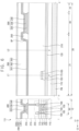
- FIG. 6 is a cross-sectional view taken along lines I-I' and II-II' of FIG. 5 .
- the display device 100 may include a functional module FM, a substrate 110, a buffer layer 120, a semiconductor element 200, a first gate insulating layer 141, a second gate insulating layer 142, an interlayer insulating layer 170, a phase compensation layer 175, a signal line 185, an etch stop layer 135, a planarization layer 210, a pixel defining layer 250, a first emission structure 300, a second emission structure 400 and a thin film encapsulation structure 260.
- a functional module FM a substrate 110, a buffer layer 120, a semiconductor element 200, a first gate insulating layer 141, a second gate insulating layer 142, an interlayer insulating layer 170, a phase compensation layer 175, a signal line 185, an etch stop layer 135, a planarization layer 210, a pixel defining layer 250, a first emission structure 300, a second emission structure 400 and a thin film encapsulation structure 260.
- the semiconductor element 200 may include an active layer 130, a first gate electrode 150, a second gate electrode 160, a source electrode 180, and a drain electrode 190.
- the first emission structure 300 may include a first lower electrode 225, a first emission layer 235 and an upper electrode 240.
- the second emission structure 400 may include a second lower electrode 220, a second emission layer 230 and the upper electrode 240.
- the thin film encapsulation structure 260 may include a first inorganic thin film encapsulation layer 261, an organic thin film encapsulation layer 262, and a second inorganic thin film encapsulation layer 263.
- the substrate 110 may also include the display area 10, the module-corresponding area 20 and the pixel circuit area 30 corresponding to those described above. That is, various components and layers of the display device 100 may also include the display area 10, the module-corresponding area 20 and the pixel circuit area 30 corresponding to those described above for the display device 100.
- the substrate 110 may include a transparent material or an opaque material.
- the substrate 110 may include a quartz substrate, a synthetic quartz substrate, a calcium fluoride substrate, an F-doped quartz substrate, and a soda-lime glass. It may include a glass substrate, a non-alkali glass substrate, and the like. These may be used alone or in combination with each other.
- the substrate 110 may be formed of (or include) a flexible transparent resin substrate.
- the substrate 110 may have a structure in which a first organic layer, a first barrier layer, a second organic layer, and a second barrier layer are sequentially stacked. Each of the first barrier layer and the second barrier layer may include an inorganic material such as silicon oxide.
- Each of the first organic layer and the second organic layer may include an organic insulating material such as a polyimide-based resin, and may have flexibility.
- the substrate 110 has been described as having four layers, the configuration of the substrate 110 is not limited thereto. In an embodiment, for example, the substrate 110 may have a single layer or a plurality of layers.
- the functional module FM may be disposed in the module-corresponding area 20, on the lower surface of the substrate 110 which is furthest from the various emission structures.
- the functional module FM may directly contact the lower surface of the substrate 110.
- elements may form an interface or boundary therebetween, without being limited thereto.
- the functional module FM may include the camera module.
- the camera module may collect light incident from outside of the display device 100, and the display device 100 may obtain an image from the camera module.
- the buffer layer 120 may be disposed on the substrate 110. That is, the buffer layer 120 may be disposed in an entirety of the display area 10 and an entirety of the module-corresponding area 20.
- the buffer layer 120 may prevent diffusion of metal atoms or impurities from the substrate 110 to the semiconductor element 200.
- the buffer layer 120 may serve to improve the flatness of the surface of the substrate 110.
- the buffer layer 120 may include silicon oxide (SiO x ), silicon nitride (SiN x ), and the like. These may be used alone or in combination with each other.
- the buffer layer 120 may be disposed only in the display area 10 and may not be disposed in the module-corresponding area 20.
- the active layer 130 may be disposed in the display area 10, on the buffer layer 120. Specifically, the active layer 130 may be disposed in the second pixel area 50 included in the display area 10.
- the active layer 130 may include a metal oxide semiconductor, an inorganic semiconductor (e.g., amorphous silicon, polysilicon) or an organic semiconductor.
- the active layer 130 may have a source region, a drain region, and a channel region positioned between the source region and the drain region in a direction along the substrate 110.
- the etch stop layer 135 may be disposed in the module-corresponding area 20, on the buffer layer 120.
- the etch stop layer 135 may be disposed in an entirety of the module-corresponding area 20.
- the etch stop layer 135 may be disposed on the same layer as the active layer 130. That is, the etch stop layer 135 may include the same material as the active layer 130.
- elements may be in a same layer as each other as respective portions of a same material layer, may form an interface with a same underlying or overlying layer, etc., without being limited thereto.
- the etch stop layer 135 may include a transparent material.
- the etch stop layer 135 may include indium gallium zinc oxide ("IGZO"), amorphous silicon, and the like. These may be used alone or in combination with each other.
- IGZO indium gallium zinc oxide
- amorphous silicon and the like. These may be used alone or in combination with each other.
- the material included in the etch stop layer 135 is not limited thereto, and the etch stop layer 135 may include other transparent materials.
- an etch rate of the etch stop layer 135 may be smaller than an etch rate of the phase compensation layer 175, which will be described later.
- At least one inorganic insulating layer may be disposed in the display area 10 on the buffer layer 120.
- the first gate insulating layer 141 may cover the active layer 130 in the display area 10 and may not be disposed in the module-corresponding area 20.
- the first gate insulating layer 141 may sufficiently cover the active layer 130 on the buffer layer 120, and may have a substantially flat top surface without creating a step around the active layer 130.
- the first gate insulating layer 141 may cover the active layer 130 on the buffer layer 120, and may be disposed along a profile of the active layer 130 with a uniform thickness.
- the first gate insulating layer 141 may include an inorganic insulating material.
- the first gate insulating layer 141 may include silicon oxide (SiO x ), silicon nitride (SiN x ), silicon carbide (SiC x ), silicon oxynitride (SiO x N y ), silicon oxycarbide (SiO x C y ), and the like. These may be used alone or in combination with each other.
- the first gate electrode 150 may be disposed in the display area 10 on the first gate insulating layer 141. Specifically, the first gate electrode 150 may be disposed in the second pixel area 50 included in the display area 10. The first gate electrode 150 may overlap the channel region of the active layer 130.
- the first gate electrode 150 may include a metal, an alloy, a metal nitride, a conductive metal oxide, a transparent conductive material, and the like. These may be used alone or in combination with each other.
- At least one inorganic insulating layer may be disposed in the display area 10 on the first gate insulating layer 141.
- the second gate insulating layer 142 may cover the first gate electrode 150 in the display area 10 and may not be disposed in the module-corresponding area 20.
- the second gate insulating layer 142 may sufficiently cover the first gate electrode 150 on the first gate insulating layer 141 and may have a substantially flat top surface without generating a step difference around the first gate electrode 150.
- the second gate insulating layer 142 may cover the first gate electrode 150 on the first gate insulating layer 141 and may be disposed along a profile of the first gate electrode 150 with a uniform thickness.
- the second gate insulating layer 142 may include an inorganic insulating material.
- the second gate insulating layer 142 may include silicon oxide, silicon nitride, silicon carbide, silicon oxynitride, silicon oxycarbide, and the like. These may be used alone or in combination with each other.
- the second gate electrode 160 may be disposed in the display area 10, on the second gate insulating layer 142. Specifically, the second gate electrode 160 may be disposed in the second pixel area 50 included in the display area 10. The second gate electrode 160 may overlap the first gate electrode 150. The first gate electrode 150 and the second gate electrode 160 may function together as a capacitor. In an embodiment, for example, the second gate electrode 160 may include a metal, an alloy, a metal nitride, a conductive metal oxide, a transparent conductive material, and the like. These may be used alone or in combination with each other.
- the interlayer insulating layer 170 may be disposed in the display area 10, on the second gate insulating layer 142.
- the interlayer insulating layer 170 may cover the second gate electrode 160 in the display area 10.
- the interlayer insulating layer 170 may sufficiently cover the second gate electrode 160 on the second gate insulating layer 142 and may have a substantially flat top surface without creating a step around the second gate electrode 160.
- the interlayer insulating layer 170 may cover the second gate electrode 160 on the second gate insulating layer 142 and may be disposed along the profile of the second gate electrode 160 with a uniform thickness.
- the interlayer insulating layer 170 may include an inorganic insulating material.
- the insulating interlayer 170 may include silicon oxide, silicon nitride, silicon carbide, silicon oxynitride, silicon oxycarbide, and the like. These may be used alone or in combination with each other.
- the interlayer insulating layer 170 may be referred to as an inorganic insulating layer.
- a phase difference between a first light L1 passing through a portion overlapping with a signal line 185, and a second light L2 passing through a portion not overlapping with the signal line 185, among the lights incident on a conventional module-corresponding area in which a functional member (e.g., a camera module) is disposed may occur.
- a flare phenomenon in which an image photographed by the camera module appears blurry may occur.
- the phase compensation layer 175 may be disposed in the module-corresponding area 20, on the etch stop layer 135. Specifically, the phase compensation layer 175 may be disposed in the transparent area 21 included in the module-corresponding area 20.
- the phase compensation layer 175 e.g., light phase compensation layer
- the phase compensation layer 175 may serve to compensate for the phase difference between a first light L1 passing through a portion overlapping the signal line 185, and a second light L2 passing through a portion not overlapping the signal line 185 (e.g., adjacent to or spaced apart from the signal line 185), among the lights incident on the module-corresponding area 20 (e.g., external light). Accordingly, an occurrence of the flare phenomenon may be reduced.
- the phase compensation layer 175 may include the same material as the interlayer insulating layer 170. That is, the phase compensation layer 175 may include an inorganic insulating material. In an embodiment, the phase compensation layer 175 may include silicon oxide, silicon nitride, and the like. When the phase compensation layer 175 includes silicon oxide, a refractive index of the phase compensation layer 175 may be about 1.5 in a visible light region. When the phase compensation layer 175 includes silicon nitride, a refractive index of the phase compensation layer 175 may be about 1.8 to about 2.0 in a visible light region.
- the source electrode 180 and the drain electrode 190 may be disposed in the display area 10, on the interlayer insulating layer 170. Specifically, the source electrode 180 and the drain electrode 190 may be disposed in the second pixel area 50 included in the display area 10.
- the source electrode 180 may be connected to the source region of the active layer 130 through a first contact hole formed by (or provided by) removing first portions of the first gate insulating layer 141, the second gate insulating layer 142 and the interlayer insulating layer 170.
- the drain electrode 190 may be connected to the drain region of the active layer 130 through a second contact hole formed by removing second portions of the first gate insulating layer 141, the second gate insulating layer 142 and the interlayer insulating layer 170.
- Each of the source electrode 180 and the drain electrode 190 may include a metal, an alloy, a metal nitride, a conductive metal oxide, a transparent conductive material, and the like. These may be used alone or in combination with each other.
- the signal line 185 may be disposed on the phase compensation layer 175.
- the signal line 185 may overlap the phase compensation layer 175.
- the signal line 185 may be electrically connected to the first lower electrode 225 through a contact hole formed by removing a portion of the planarization layer 210 positioned in the module-corresponding area 20.
- the signal line 185 may extend from the module-corresponding area 20 to the pixel circuit area 30, to be electrically connected to the first pixel circuit structure 501. That is, the signal line 185 connects the first emission structure 300 to the pixel circuit area 30.
- a thickness of the signal line 185 along the thickness direction may be smaller than a thickness of each of the source electrode 180 and the drain electrode 190.
- the signal line 185 may be substantially transparent.
- the signal line 185 may include a conductive metal oxide, a transparent conductive material, and the like.
- materials that can be used for the signal line 185 may be indium tin oxide ("ITO"), indium zinc oxide (“IZO"), indium gallium oxide (“IGO”), tin oxide (“SnO 2 "), zinc oxide (“ZnO”), and the like. These may be used alone or in combination with each other.
- the signal line 185 may include indium tin oxide.
- the refractive index of the signal line 185 may be about 1.9 or more in a visible light region.
- the planarization layer 210 may be disposed on the source electrode 180 and drain electrode 190 disposed in the display area 10 and on the etch stop layer 135 disposed in the module-corresponding area 20. That is, the planarization layer 210 may extend from the display area 10 to the module-corresponding area 20.
- the planarization layer 210 may cover the source electrode 180 and the drain electrode 190 in the display area 10, and may cover the phase compensation layer 175 and the signal line 185 in the module-corresponding area 20.
- the planarization layer 210 may have a relatively large thickness.
- the planarization layer 210 may include an organic insulating material or an inorganic insulating material. In an embodiment, the planarization layer 210 may include an organic insulating material.
- Examples of the organic insulating material that can be used for the planarization layer 210 may be a photoresist, a polyacrylic resin, a polyimide-based resin, a polyamide-based resin, a siloxane-based resin, an acrylic resin, an epoxy-based resin, and the like. These may be used alone or in combination with each other. Where the planarization layer 210 includes a substantially transparent siloxane-based resin, the planarization layer 210 may be referred to as an organic insulating layer.
- a refractive index of the planarization layer 210 may be greater than a refractive index of the phase compensation layer 175 and less than that of the signal line 185. In an embodiment, for example, a refractive index of the planarization layer 210 may be about 1.65 in a visible light region.
- the phase compensation layer 175 may include silicon oxide
- the signal line 185 may include indium tin zinc oxide.
- the second lower electrode 220 may be disposed in the display area 10, on the planarization layer 210. Specifically, the second lower electrode 220 may be disposed in the second pixel area 50 included in the display area 10. The second lower electrode 220 may be connected to the drain electrode 190 through a contact hole formed by removing a portion of the planarization layer 210. The second lower electrode 220 may be electrically connected to the semiconductor element 200.
- the second lower electrode 220 may include a metal, an alloy, a metal nitride, a conductive metal oxide, a transparent conductive material, and the like. These may be used alone or in combination with each other.
- the second lower electrode 220 may have a stacked structure of ITO/Ag/ITO.
- the first lower electrode 225 may be disposed in the module-corresponding area 20, on the planarization layer 210. Specifically, the first lower electrode 225 may be disposed in the first pixel area 40 included in the module-corresponding area 20. As described above, the first lower electrode 225 may be connected to the signal line 185 through a contact hole formed by removing a portion of the planarization layer 210 (see FIG. 5 ).
- the first lower electrode 225 may include a metal, an alloy, a metal nitride, a conductive metal oxide, a transparent conductive material, and the like. These may be used alone or in combination with each other.
- the first lower electrode 225 may have the same structure as the second lower electrode 220. In an embodiment, the first lower electrode 225 may have a structure different from a structure of the second lower electrode 220.
- the pixel defining layer 250 may be disposed on a portion of the display area 10 and a portion of the module-corresponding area 20, on the planarization layer 210. That is, the pixel defining layer 250 may not be disposed in the transparent area 21.
- the pixel defining layer 250 may expose a portion of the second lower electrode 220 in the display area 10 to outside the pixel defining layer 250, and may expose a portion of the first lower electrode 225 in the module-corresponding area 20 to outside the pixel defining layer 250.
- an opening OP exposing layers in the transparent area 21 to outside the pixel defining layer 250 may be formed in (or defined by) the pixel defining layer 250.
- the pixel defining layer 250 may include an organic insulating material or an inorganic insulating material. In an embodiment, the pixel defining layer 250 may include an organic insulating material.
- the second emission layer 230 may be disposed on the second lower electrode 220.
- the first emission layer 235 may be disposed on the first lower electrode 225.
- Each of the first emission layer 235 and the second emission layer 230 may be formed using at least one of emission materials that emit different color lights (e.g., red light, green light, blue light, and the like) according to sub-pixels.
- the upper electrode 240 may be disposed in an entirety of the display area 10 and the module-corresponding area 20, on the substrate 110.
- the upper electrode 240 may be disposed along the profile of the first emission layer 235, the second emission layer 230, and the pixel defining layer 250.
- the upper electrode 240 may include a metal, an alloy, a metal nitride, a conductive metal oxide, a transparent conductive material, and the like. These may be used alone or in combination with each other.
- the first inorganic thin film encapsulation layer 261 may be disposed on the upper electrode 240.
- the first inorganic thin film encapsulation layer 261 may be disposed in an entirety of the display area 10 and an entirety of the module-corresponding area 20.
- the first inorganic thin film encapsulation layer 261 may prevent (or reduce) the first emission structure 300 and the second emission structure 400 from being deteriorated due to penetration of moisture, oxygen, and the like.
- the first inorganic thin film encapsulation layer 261 may also function to protect the first emission structure 300 and the second emission structure 400 from external impact.
- the first inorganic thin film encapsulation layer 261 may include an inorganic insulating material having flexibility.
- the organic thin film encapsulation layer 262 may be disposed on the first inorganic thin film encapsulation layer 261.
- the organic thin film encapsulation layer 262 may be disposed in an entirety of the display area 10 and the module-corresponding area 20.
- the organic thin film encapsulation layer 262 may improve the flatness of the display device 100, and may protect the first emission structure 300 and the second emission structure 400 together with the first inorganic thin film encapsulation layer 261.
- the organic thin film encapsulation layer 262 may include an organic insulating material having flexibility.
- the second inorganic thin film encapsulation layer 263 may be disposed on the organic thin film encapsulation layer 262.
- the second inorganic thin film encapsulation layer 263 may be disposed in an entirety of the display area 10 and an entirety of the module-corresponding area 20.
- the second inorganic thin film encapsulation layer 263 may be used together with the first inorganic thin film encapsulation layer 261 to prevent the first emission structure 300 and the second emission structure 400 from being deteriorated due to penetration of moisture, oxygen, and the like.
- the second inorganic thin film encapsulation layer 263 may also perform a function to protect the first emission structure 300 and the second emission structure 400 together with the first inorganic thin film encapsulation layer 261 and the organic thin film encapsulation layer 262 from external impact.
- the second inorganic thin film encapsulation layer 263 may include an inorganic insulating material having flexibility.
- phase compensation layer 175 including an inorganic insulating material is disposed in the module-corresponding area 20, on the etch stop layer 135, an occurrence of the flare phenomenon may be reduced.
- phase compensation layer 175 in the process of patterning the phase compensation layer 175, a thickness of the phase compensation layer 175 may become non-uniform.
- etch stop layer 135 including a transparent material is disposed in the module-corresponding area 20, between the substrate 110 and the phase compensation layer 175, a thickness non-uniformity of the phase compensation layer 175 in the large area display device may be improved.
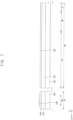
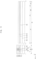
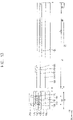
- FIG. 7 , 8 , 9 , 10 , 11 , 12 , 13 , 14 , 15 , and 16 are cross-sectional views illustrating embodiments of structures in a method of manufacturing (or providing) the display device 100 of FIG. 6 .
- the substrate 110 including a transparent material may be formed on a rigid glass substrate 105 (e.g., a base layer).
- the substrate 110 may be formed using a flexible transparent resin substrate.
- the substrate 110 may be formed using a quartz substrate, a synthetic quartz substrate, a glass substrate, and the like.
- the rigid glass substrate 105 may be omitted.
- the substrate 110 when the substrate 110 includes a transparent material, since the substrate 110 is thin and flexible, the substrate 110 may be formed on the rigid glass substrate 105 to support the formation of the semiconductor element 200, the first emission structure 300, the second emission structure 400, and the thin film encapsulation structure 260, and the like. As will be described later, after the thin film encapsulation structure 260 is formed, the rigid glass substrate 105 may be removed.
- the substrate 110 may include the display area 10, the module-corresponding area 20, and the pixel circuit area 30.
- the buffer layer 120 may be formed on the substrate 110.
- the buffer layer 120 may be formed in an entirety of the display area 10 and an entirety of the module-corresponding area 20. According to the type of the substrate 110, two or more buffer layers 120 may be formed on the substrate 110 or the buffer layer 120 may not be formed.
- the buffer layer 120 may be formed using silicon oxide, silicon nitride, and the like.
- the active layer 130 may be formed in the display area 10 on the buffer layer 120.
- the active layer 130 may be formed using a metal oxide semiconductor, an inorganic semiconductor, or an organic semiconductor.
- the active layer 130 may include a source region, a drain region, and a channel region positioned between the source region and the drain area.
- the etch stop layer 135 may be formed in the module-corresponding area 20, on the buffer layer 120. That is, the etch stop layer 135 may be formed on the same layer as the active layer 130. In addition, the etch stop layer 135 may be formed in an entirety of the module-corresponding area 20. In an embodiment, for example, the etch stop layer 135 may be formed using a transparent material. In an embodiment, the etch stop layer 135 may be formed using indium gallium zinc oxide, amorphous silicon, and the like.
- the etch stop layer 135 may be formed in the same process as the active layer 130. That is, the etch stop layer 135 may be simultaneously formed using the same material as the active layer 130. In an embodiment, the etch stop layer 135 may be formed in a process different from a process of the active layer 130. In an embodiment, for example, after the active layer 130 is formed, the etch stop layer 135 may be formed. In this case, the etch stop layer 135 may be formed using a material different from a material of the active layer 130.
- the first gate insulating layer 141 may be formed on the buffer layer 120.
- the first gate insulating layer 141 may cover the active layer 130 in the display area 10 and may extend to the module-corresponding area 20. That is, the first gate insulating layer 141 may be formed in an entirety of the display area 10 and an entirety of the module-corresponding area 20.
- the first gate insulating layer 141 may be formed using silicon oxide, silicon nitride, silicon oxynitride, and the like.
- the first gate electrode 150 may be formed in the display area 10 on the first gate insulating layer 141.
- the first gate electrode 150 may be formed to overlap the channel region of the active layer 130.
- the first gate electrode 150 may be formed using a metal, an alloy, a metal nitride, a conductive metal oxide, a transparent conductive material, and the like.
- the second gate insulating layer 142 may be formed on the first gate insulating layer 141.
- the second gate insulating layer 142 may cover the first gate electrode 150 in the display area 10 and may extend to the module-corresponding area 20. That is, the second gate insulating layer 142 may be formed in an entirety of the display area 10 and an entirety of the module-corresponding area 20.
- the second gate insulating layer 142 may be formed using silicon oxide, silicon nitride, silicon oxynitride, and the like.
- the first gate insulating layer 141 and the second gate insulating layer 142 disposed in the module-corresponding area 20 may be removed. Removal of the first gate insulating layer 141 and the second gate insulating layer 142 from the module-corresponding area 20 exposes the etch stop layer 135 to outside the first gate insulating layer 141 and the second gate insulating layer 142.
- the second gate electrode 160 may be formed in the display area 10, on the second gate insulating layer 142.
- the second gate electrode 160 may overlap the first gate electrode 150.
- the second gate electrode 160 may be formed using a metal, an alloy, a metal nitride, a conductive metal oxide, a transparent conductive material, and the like.
- the interlayer insulating layer 170 may be disposed on the second gate insulating layer 142.
- the interlayer insulating layer 170 may cover the second gate electrode 160 in the display area 10 and may extend to the module-corresponding area 20. That is, the interlayer insulating layer 170 may be formed in an entirety of the display area 10 and an entirety of the module-corresponding area 20.
- the interlayer insulating layer 170 may be formed using silicon oxide, silicon nitride, silicon oxynitride, and the like.
- the source electrode 180 and the drain electrode 190 may be formed in the display area 10 on the interlayer insulating layer 170.
- the source electrode 180 may be connected to the source region of the active layer 130 through a first contact hole formed by removing a first portion of each of the first gate insulating layer 141, the second gate insulating layer 142 and the interlayer insulating layer 170.
- the drain electrode 190 may be connected to the drain region of the active layer 130 through a second contact hole formed by removing a second portion of each of the first gate insulating layer 141, the second gate insulating layer 142 and the interlayer insulating layer 170.
- Each of the source electrode 180 and the drain electrode 190 may be formed using a metal, an alloy, a metal nitride, a conductive metal oxide, a transparent conductive material, and the like.
- the semiconductor element 200 including the active layer 130, the first gate electrode 150, the second gate electrode 160, the source electrode 180 and the drain electrode 190, may be formed in the second pixel area 50.
- a conductive film 184 may be formed in the module-corresponding area 20, on the interlayer insulating layer 170.
- the conductive film 184 may be formed using a conductive metal oxide, a transparent conductive material, and the like.
- the conductive film 184 may be formed using ITO, IZO, IGO, SnO 2 , ZnO, and the like.
- the signal line 185 may be formed by patterning the conductive film 184 (e.g., signal line material layer).
- the signal line 185, the source electrode 180, and the drain electrode 190 may be formed on the same layer, but is not limited thereto, and may be formed in different processes using different materials from each other. In an embodiment, for example, after the source electrode 180 and the drain electrode 190 are formed, the signal line 185 may be formed.
- the phase compensation layer 175 may be formed by patterning the interlayer insulating layer 170 disposed in the module-corresponding area 20. Specifically, the phase compensation layer 175 may be formed at a location corresponding to the signal line 185, using the signal line 185 as a mask. That is, after the phase compensation layer 175 (e.g., phase compensation pattern) is formed, an upper surface of the etch stop layer 135 that does not overlap the signal line 185 in the module-corresponding area 20, may be exposed to outside the interlayer insulating layer 170 (or the phase compensation pattern) and the signal line 185. However, in an embodiment, a portion of the interlayer insulating layer 170 that does not overlap the signal line 185 may remain in the module-corresponding area 20.
- the phase compensation layer 175 e.g., phase compensation pattern
- the phase compensation layer 175 may be formed using silicon oxide, silicon nitride, and the like. That is, the phase compensation layer 175 may be formed using the same material as the interlayer insulating layer 170.
- the planarization layer 210 may be formed on the interlayer insulating layer 170 and the etch stop layer 135. That is, the planarization layer 210 may cover the source electrode 180 and the drain electrode 190 in the display area 10 and may extend to the module-corresponding area 20. The planarization layer 210 may cover the phase compensation layer 175 and the signal line 185 in the module-corresponding area 20.
- the planarization layer 210 may be formed using a photoresist, a polyacrylic resin, a polyimide-based resin, a polyamide-based resin, a siloxane-based resin, an acrylic resin, an epoxy-based resin, and the like.
- the planarization layer 210 may be formed using a substantially transparent siloxane-based resin.
- the second lower electrode 220 may be formed in the display area 10, on the planarization layer 210.
- the first lower electrode 225 may be formed in the module-corresponding area 20, on the planarization layer 210.
- the second lower electrode 220 may be connected to the drain electrode 190 through a contact hole formed by removing a portion of the planarization layer 210.
- the first lower electrode 225 may be connected to the signal line 185 through a contact hole formed by removing a portion of the planarization layer 210 (see box surrounding 'x' in FIG. 5 ).
- Each of the first lower electrode 225 and the second lower electrode 220 may be formed using a metal, an alloy, a metal nitride, a conductive metal oxide, a transparent conductive material, and the like.
- each of the first lower electrode 225 and the second lower electrode 220 may have a stacked structure of ITO/Ag/ITO.
- the pixel defining layer 250 may be formed in the display area 10 and a portion of the module-corresponding area 20, on the planarization layer 210.
- the pixel defining layer 250 may expose a portion of the second lower electrode 220 in the display area 10, and may expose a portion of the first lower electrode 225 in the module-corresponding area 20.
- the opening OP exposing layers in the transparent area 21 may be formed in the pixel defining layer 250.
- the pixel defining layer 250 may be formed using an organic insulating material.
- the second emission layer 230 may be formed on the second lower electrode 220, and the first emission layer 235 may be formed on the first lower electrode 225.
- Each of the first emission layer 235 and the second emission layer 230 may be formed using at least one of light emitting materials capable of emitting light of different colors according to sub-pixels.
- the upper electrode 240 may be formed in an entirety of the display area 10 and an entirety of the module-corresponding area 20 on the substrate 110.
- the upper electrode 240 may be formed along the profile of the first emission layer 235, the second emission layer 230, and the pixel defining layer 250.
- the upper electrode 240 may be formed using a metal, an alloy, a metal nitride, a conductive metal oxide, a transparent conductive material, and the like.
- the second emission structure 400 including the second lower electrode 220, the second emission layer 230 and the upper electrode 240 may be formed in the second pixel area 50, and the first emission structure 300 including the first lower electrode 225, the first emission layer 235 and the upper electrode 240 may be formed in the first pixel area 40.
- the first inorganic thin film encapsulation layer 261 may be formed in the display area 10 and the module-corresponding area 20, on the upper electrode 240. In an embodiment, for example, the first inorganic thin film encapsulation layer 261 may be formed using an inorganic insulating material having flexibility.
- the organic thin film encapsulation layer 262 may be formed in the display area 10 and the module-corresponding area 20, on the first inorganic thin film encapsulation layer 261. In an embodiment, for example, the organic thin film encapsulation layer 262 may be formed using an organic insulating material having flexibility.
- the second inorganic thin film encapsulation layer 263 may be formed on the organic thin film encapsulation layer 262. The second inorganic thin film encapsulation layer 263 may be formed using an inorganic insulating material having flexibility.
- the thin film encapsulation structure 260 including the first inorganic thin film encapsulation layer 261, the organic thin film encapsulation layer 262, and the second inorganic thin film encapsulation layer 263 may be formed.
- the glass substrate 105 may be removed from the substrate 110 to expose a lower surface of the substrate 110.
- the functional module FM may be formed in the module-corresponding area 20, on the lower surface of the substrate 110.
- the functional module FM may include the camera module and the like.
- the display device 100 shown in FIGS. 1, 2 , 3 , 4 , 5 , and 6 may be provided.
- FIG. 17 is a cross-sectional view illustrating an embodiment of a display device 1000.
- the display device 1000 may include a functional module FM, a substrate 110, a buffer layer 120, a semiconductor element 200, a first gate insulating layer 141, a second gate insulating layer 142, an interlayer insulating layer 170, a phase compensation layer 175, a signal line 185, an etch stop layer 135, a planarization layer 210, a pixel defining layer 250, a first emission structure 300, a second emission structure 400 and a thin film encapsulation structure 260.
- the display device 1000 of FIG. 17 may be substantially the same as or similar to the display device 100 described with reference to FIG. 6 except for the etch stop layer 135.
- overlapping descriptions will be omitted.
- the etch stop layer 135 may be disposed in the module-corresponding area 20, on the buffer layer 120.
- the etch stop layer 135 may be patterned to define an etch stop pattern which overlaps each of the phase compensation layer 175 and the signal line 185.
- the etch stop layer 135 may include amorphous silicon.
- the buffer layer 120 may be exposed to outside the phase compensation layer 175, the signal line 185 and the etch stop layer 135, within the module-corresponding area 20.
- the etch stop layer 135 and the active layer 130 are formed on the same layer, the invention is not limited thereto, and the etch stop layer 135 and the active layer 130 may be formed using different materials and in different processes. In an embodiment, for example, after the active layer 130 is formed, the etch stop layer 135 may be formed. Specifically, after the phase compensation layer 175 is patterned to provide a phase compensation pattern, the etch stop layer 135 may be patterned to provide an etch stop pattern.
- FIG. 18 is a cross-sectional view illustrating an embodiment of a display device 1100.
- the display device 1100 may include a functional module FM, a substrate 110, a buffer layer 120, a semiconductor element 200, a first gate insulating layer 141, a second gate insulating layer 142, an interlayer insulating layer 170, a phase compensation layer 175, a signal line 185, an etch stop layer 135, a planarization layer 210, a pixel defining layer 250, a first emission structure 300, a second emission structure 400, a thin film encapsulation structure 260.
- the display device 1100 of FIG. 18 may be substantially the same as or similar to the display device 100 described with reference to FIG. 6 except for the first gate insulating layer 141 and the second gate insulating layer 142 disposed in the module-corresponding area 20.
- overlapping descriptions will be omitted.
- At least one inorganic insulating layer may be disposed on the buffer layer 120.
- the first gate insulating layer 141 may be disposed on the buffer layer 120
- the second gate insulating layer 142 may be disposed on the first gate insulating layer 141.
- the first gate insulating layer 141 and the second gate insulating layer 142 may be disposed in an entirety of the display area 10 and an entirety of the module-corresponding area 20. That is, the first gate insulating layer 141 and the second gate insulating layer 142 in the module-corresponding area 20 may remain on the substrate 110, without being removed.
- each of the first gate insulating layer 141 and the second gate insulating layer 142 may have a multilayer structure including a plurality of insulating layers.
- the etch stop layer 135 may be disposed in the module-corresponding area 20, on the second gate insulating layer 142. In addition, the etch stop layer 135 may be disposed in an entirety of the module-corresponding area 20 to face the substrate with both the first gate insulating layer 141 and the second gate insulating layer 142 therebetween.
- the etch stop layer 135 may be formed in a process different from a process of the active layer 130. In an embodiment, for example, after the active layer 130 is formed, the etch stop layer 135 may be formed. In this case, the etch stop layer 135 and the active layer 130 may include different materials.
- FIG. 19 is a cross-sectional view illustrating an embodiment of a display device 1200.
- the display device 1200 may include a functional module FM, a substrate 110, a buffer layer 120, a semiconductor element 200, a first gate insulating layer 141, and a second gate insulating layer 142, an interlayer insulating layer 170, a phase compensation layer 175, a signal line 185, an etch stop layer 135, a planarization layer 210, a pixel defining layer 250, a first emission structure 300, a second emission structure 400 and a thin film encapsulation structure 260.
- the display device 1200 of FIG. 19 may be substantially the same as or similar to the display device 1100 described with reference to FIG. 18 except for the etch stop layer 135 disposed in the module-corresponding area 20.
- overlapping descriptions will be omitted.
- the etch stop layer 135 may be disposed in the module-corresponding area 20, on the second gate insulating layer 142. In addition, referring back to FIG. 17 , the etch stop layer 135 may be patterned to overlap each of the phase compensation layer 175 and the signal line 185.
- One or more embodiment of the present disclosure can be applied to various display devices that may include an image-generating device.
- the present disclosure can be applied to high-resolution smartphones, mobile phones, smart pads, smart watches, tablet PCs, in-vehicle navigation systems, televisions, computer monitors, notebook computers, and the like.
Landscapes
- Engineering & Computer Science (AREA)
- Physics & Mathematics (AREA)
- Microelectronics & Electronic Packaging (AREA)
- Computer Hardware Design (AREA)
- Theoretical Computer Science (AREA)
- Optics & Photonics (AREA)
- General Engineering & Computer Science (AREA)
- General Physics & Mathematics (AREA)
- Human Computer Interaction (AREA)
- Manufacturing & Machinery (AREA)
- Geometry (AREA)
- Electroluminescent Light Sources (AREA)
- Devices For Indicating Variable Information By Combining Individual Elements (AREA)
Abstract
Description
- Embodiments relate generally to a display device. More particularly, embodiments relate to a display device that provides visual information.
- A flat panel display device is used as a display device replacing a cathode ray in a display device, due to characteristics such as light weight and thinness. Representative examples of such flat panel display devices are a liquid crystal display device ("LCD") and an organic light emitting display device ("OLED").
- The display device may include a module-corresponding area in which a functional module is disposed, and a display area surrounding the module-corresponding area and in which emission structures are disposed. Here, the functional module may be disposed on a lower surface of a substrate included in the display device. A display device capable of displaying an image by arranging emission structures in the module-corresponding area has been developed.
- Embodiments provide a display device with improved display quality.
- An embodiment of a display device includes a substrate including a (functional) module-corresponding area, a display area adjacent to the module-corresponding area, and a pixel circuit area at a side of the display area, an inorganic insulating layer in the display area on the substrate, a (light) phase compensation layer in the module-corresponding area, on the substrate, and including a same material as the inorganic insulating layer, a signal line in the module-corresponding area, on the phase compensation layer and extending from the module-corresponding area to the pixel circuit area, and an organic insulating layer on the inorganic insulating layer and extending from the display area to the module-corresponding area to cover the signal line and the phase compensation layer.
- In an embodiment, the display device may further include an etch stop layer in the module-corresponding area, between the substrate and the phase compensation layer, and including a transparent material.
- In an embodiment, an etch rate of the etch stop layer may be smaller than an etch rate of the phase compensation layer.
- In an embodiment, the etch stop layer may include indium gallium zinc oxide ("IGZO") or amorphous silicon.
- In an embodiment, the etch stop layer may be in an entirety of the module-corresponding area.
- In an embodiment, the etch stop layer may be a pattern which overlaps each of the phase compensation layer and the signal line.
- In an embodiment, the signal line may include a conductive metal oxide or a transparent conductive material.
- In an embodiment, the transparent conductive material may include indium tin oxide ("ITO"), indium zinc oxide ("IZO") or indium gallium oxide ("IGO").
- In an embodiment, the inorganic insulating layer may include silicon oxide or silicon nitride.
- In an embodiment, a refractive index of the organic insulating layer may be greater than a refractive index of the phase compensation layer and smaller than a refractive index of the signal line.
- In an embodiment, a refractive index of the signal line may be about 1.9 or more in a visible light region.
- In an embodiment, the display device may further include a functional module in the module-corresponding area, on a lower surface of the substrate.
- In an embodiment, the functional module may include a camera module, a face recognition sensor module, a pupil recognition sensor module, an acceleration sensor module, a proximity sensor module, an infrared sensor module or an illuminance sensor module.
- In an embodiment, the display device may further include a pixel circuit structure in the pixel circuit area, on the substrate, and including a semiconductor element, and an emission structure in the module-corresponding area, on the substrate.
- In an embodiment, the signal line may electrically connect the pixel circuit structure and the emission structure.
- An embodiment of a display device includes a substrate including a module-corresponding area, a display area adjacent to the module-corresponding area, and a pixel circuit area at a side of the display area, a first inorganic insulating layer in the display area and the module-corresponding area, on the substrate, a second inorganic insulating layer in the display area, on the first inorganic insulating layer, a (light) phase compensation layer in the module-corresponding area, on the substrate, and including a same material as the second inorganic insulating layer, a signal line in the module-corresponding area, on the phase compensation layer, and extending from the module-corresponding area to the pixel circuit area, and an organic insulating layer on the second inorganic insulating layer and extending from the display area to the module-corresponding area to cover the signal line and the phase compensation layer.
- In an embodiment, the display device may further include an etch stop layer in the module-corresponding area, on the first inorganic insulating layer, and including a transparent material.
- In an embodiment, an etch rate of the etch stop layer may be smaller than an etch rate of the phase compensation layer.
- In an embodiment, the etch stop layer may include indium gallium zinc oxide or amorphous silicon.
- In an embodiment, each of the first inorganic insulating layer and the second inorganic insulating layer may include silicon oxide or silicon nitride.
- At least some of the above and other features of the invention are set out in the claims.
- In one or more embodiments of a display device, as a light phase compensation layer including an inorganic insulating material is in a functional module area, an occurrence of a flare phenomenon may be reduced.
- In addition, as a etch stop layer including a transparent material is in the functional module area between the substrate and the phase compensation layer, a non-uniformity of a thickness of the phase compensation layer in a large-area display device may be improved.
- Illustrative, non-limiting embodiments will be more clearly understood from the following detailed description in conjunction with the accompanying drawings.
-
FIG. 1 and 2 are perspective views illustrating an embodiment of a display device. -
FIG. 3 is a plan view illustrating the display device ofFIG. 1 . -
FIG. 4 and5 are partially enlarged plan views illustrating an embodiment of area 'A' ofFIG. 3 . -
FIG. 6 is a cross-sectional view taken along lines I-I' and II-II' ofFIG. 5 . -
FIG. 7 ,8 ,9 ,10 ,11 ,12 ,13 ,14 ,15 , and16 are cross-sectional views illustrating embodiments of structures provided by a method of manufacturing the display device ofFIG. 6 . -
FIG. 17 is a cross-sectional view illustrating an embodiment of a display device. -
FIG. 18 is a cross-sectional view illustrating an embodiment of a display device. -
FIG. 19 is a cross-sectional view illustrating an embodiment of a display device. - Hereinafter, embodiments of the present disclosure will be explained in detail with reference to the accompanying drawings. The same reference numerals are used for the same components in the drawings, and redundant descriptions of the same components will be omitted.
- It will be understood that when an element is referred to as being related to another element such as being "on" another element, it can be directly on the other element or intervening elements may be present therebetween. In contrast, when an element is referred to as being related to an element such as being "directly on" another element, there are no intervening elements present.
- It will be understood that, although the terms "first," "second," "third" etc. may be used herein to describe various elements, components, regions, layers and/or sections, these elements, components, regions, layers and/or sections should not be limited by these terms. These terms are only used to distinguish one element, component, region, layer or section from another element, component, region, layer or section. Thus, "a first element," "component," "region," "layer" or "section" discussed below could be termed a second element, component, region, layer or section without departing from the teachings herein.
- The terminology used herein is for the purpose of describing particular embodiments only and is not intended to be limiting. As used herein, "a", "an," "the," and "at least one" do not denote a limitation of quantity, and are intended to include both the singular and plural, unless the context clearly indicates otherwise. For example, "an element" has the same meaning as "at least one element," unless the context clearly indicates otherwise. "At least one" is not to be construed as limiting "a" or "an." "Or" means "and/or." As used herein, the term "and/or" includes any and all combinations of one or more of the associated listed items. It will be further understood that the terms "comprises" and/or "comprising," or "includes" and/or "including" when used in this specification, specify the presence of stated features, regions, integers, steps, operations, elements, and/or components, but do not preclude the presence or addition of one or more other features, regions, integers, steps, operations, elements, components, and/or groups thereof.
- Furthermore, relative terms, such as "lower" or "bottom" and "upper" or "top," may be used herein to describe one element's relationship to another element as illustrated in the Figures. It will be understood that relative terms are intended to encompass different orientations of the device in addition to the orientation depicted in the Figures. For example, if the device in one of the figures is turned over, elements described as being on the "lower" side of other elements would then be oriented on "upper" sides of the other elements. The term "lower," can therefore, encompasses both an orientation of "lower" and "upper," depending on the particular orientation of the figure. Similarly, if the device in one of the figures is turned over, elements described as "below" or "beneath" other elements would then be oriented "above" the other elements. The terms "below" or "beneath" can, therefore, encompass both an orientation of above and below.
- "About" or "approximately" as used herein is inclusive of the stated value and means within an acceptable range of deviation for the particular value as determined by one of ordinary skill in the art, considering the measurement in question and the error associated with measurement of the particular quantity (i.e., the limitations of the measurement system). For example, "about" can mean within one or more standard deviations, or within ± 30%, 20%, 10% or 5% of the stated value. Unless otherwise defined, all terms (including technical and scientific terms) used herein have the same meaning as commonly understood by one of ordinary skill in the art to which this disclosure belongs. It will be further understood that terms, such as those defined in commonly used dictionaries, should be interpreted as having a meaning that is consistent with their meaning in the context of the relevant art and the present disclosure, and will not be interpreted in an idealized or overly formal sense unless expressly so defined herein.
- Embodiments are described herein with reference to cross section illustrations that are schematic illustrations of embodiments. As such, variations from the shapes of the illustrations as a result, for example, of manufacturing techniques and/or tolerances, are to be expected. Thus, embodiments described herein should not be construed as limited to the particular shapes of regions as illustrated herein but are to include deviations in shapes that result, for example, from manufacturing. For example, a region illustrated or described as flat may, typically, have rough and/or nonlinear features. Moreover, sharp angles that are illustrated may be rounded. Thus, the regions illustrated in the figures are schematic in nature and their shapes are not intended to illustrate the precise shape of a region and are not intended to limit the scope of the present claims.
-
FIG. 1 and 2 are perspective views illustrating an embodiment of adisplay device 100.FIG. 3 is a plan view illustrating thedisplay device 100 ofFIG. 1 . - Referring to
FIGS. 1, 2 , and3 , thedisplay device 100 may include adisplay area 10, a module-corresponding area 20 (e.g., functional module area), and apixel circuit area 30. - The
display area 10 is adjacent to the module-correspondingarea 20 and may surround at least a portion of the module-correspondingarea 20. Thepixel circuit area 30 may be positioned at one side of thedisplay area 10. In addition, thepixel circuit area 30 may be adjacent to one side of the module-correspondingarea 20. That is, first to third sides of the module-correspondingarea 20 may be adjacent to thedisplay area 10, and a fourth side of the module-correspondingarea 20 may be adjacent to thepixel circuit area 30, so as to be surrounded by thedisplay area 10 together with thepixel circuit area 30. - The
display device 100 may be divided into (or include) a first surface S1 and a second surface S2. The first surface S1 may correspond to a surface on which an image is displayed (e.g., display surface). The second surface S2 may correspond to a surface on which an image is not displayed. The module-correspondingarea 20 may be in and form a part of thedisplay area 10. An image may be displayed and/or light may be emitted at the module-correspondingarea 20, without being limited thereto. - The
display device 100 may include a functional module FM. The functional module FM may be disposed to overlap (or correspond to) the module-correspondingarea 20, on the second surface S2. In an embodiment, an image may be displayed at both a portion of the first surface S1 overlapping the module-correspondingarea 20 and a portion of the first surface S1 overlapping thedisplay area 10. In an embodiment, for example, the functional module FM may provide a function to thedisplay device 100 and may include a camera module, a face recognition sensor module, a pupil recognition sensor module, an acceleration sensor module, a proximity sensor module, an infrared sensor module, an illuminance sensor module, and the like. In an embodiment, the functional module FM may include the camera module. In this case, the functional module FM may capture an image by capturing external light incident to thedisplay device 100 through a portion of the first surface S1 overlapping the module-correspondingarea 20, to provide an image-capturing function to thedisplay device 100. - However, although a shape of the functional module FM is shown as having a rectangular planar shape, the planar shape of the functional module FM is not limited thereto. In an embodiment, for example, the functional module FM may have a triangular planar shape, a rhombus planar shape, a polygonal planar shape, a track-type planar shape, a circular planar shape, or an elliptical planar shape. In addition, when a planar shape of the functional module FM is changed, a planar shape of the module-corresponding
area 20 may also be changed according to an outer shape of the functional module FM. -
FIG. 4 and5 are partially enlarged plan views illustrating embodiments of area 'A' ofFIG. 3 . - Referring to
FIG. 4 , thedisplay area 10 may include (or correspond to) asecond pixel area 50, and the module-correspondingarea 20 may include atransparent area 21 and afirst pixel area 40. In addition, thepixel circuit area 30 may include a firstpixel circuit area 31 provided in plural including a plurality firstpixel circuit areas 31 and a secondpixel circuit area 32 provided in plural including a plurality of secondpixel circuit areas 32. - The
second pixel area 50 may include a plurality of secondsub-pixel areas first pixel area 40 may include a plurality of firstsub-pixel areas display area 10, without being limited thereto. The pixel area (or sub-pixel area) may otherwise be referred to as a light emission area. - In an embodiment, for example, the
second sub-pixel areas red pixel area 51 in which a red emission structure R (e.g., asecond emission structure 400 ofFIG. 6 ) emitting red light is disposed, a secondgreen pixel area 52 in which a green emission structure G emitting green light is disposed, and a secondblue pixel area 53 in which a blue emission structure B emitting blue light is disposed. In addition, thefirst sub-pixel areas red pixel area 41 in which a red emission structure R (e.g., afirst emission structure 300 ofFIG. 6 ) emitting red light is disposed, a firstgreen pixel area 42 in which a green emission structure G emitting green light is disposed, and a firstblue pixel area 43 in which a blue emission structure B emitting blue light is disposed. - The plurality of second
sub-pixel areas display area 10. The plurality of firstsub-pixel areas area 20. That is, the emission structures R, G, and B may be repeatedly arranged in thedisplay area 10, and the emission structures R, G, and B may be repeatedly arranged in the module-correspondingarea 20. - In the module-corresponding
area 20, a portion other than the plurality of firstsub-pixel areas transparent area 21. An opening OP may be positioned in thetransparent area 21. In addition, the functional module FM may collect light incident from an outside through the opening OP. - The first
pixel circuit areas 31 may be positioned adjacent to a first portion (e.g., thedisplay area 10 positioned to a left of the module-correspondingarea 20 inFIG. 4 ) of thedisplay area 10 in thepixel circuit area 30, and may be arranged along a first direction D1. The secondpixel circuit areas 32 may be positioned adjacent to a second portion (e.g., thedisplay area 10 positioned to a right of the module-correspondingarea 20 inFIG. 4 ) of thedisplay area 10 in thepixel circuit area 30, and may be arranged along the first direction D1. Thepixel circuit area 30 may be adjacent to both thedisplay area 10 and the module-correspondingarea 20 along a second direction D2 crossing the first direction D1. A thickness direction of thedisplay device 100 and various components and layers thereof, may be defined along a third direction which crosses each of the first direction D1 and the second direction D2. - A pixel circuit structure (e.g., a first
pixel circuit structure 501 ofFIG. 5 ) electrically connected to an emission structure disposed in the module-correspondingarea 20 may be disposed in the first and secondpixel circuit areas pixel circuit structure 502 ofFIG. 5 ) electrically connected to an emission structure disposed in thedisplay area 10 may be disposed in thedisplay area 10. That is, a pixel circuit structure electrically connected to the emission structure disposed in the module-correspondingarea 20 may not be disposed in the module-corresponding area 20 (e.g., may be excluded from the module-corresponding area 20). - Referring to
FIG. 5 , the secondpixel circuit structure 502 may be disposed in thedisplay area 10. The secondpixel circuit structure 502 may include at least one semiconductor element 200 (seeFIG. 6 ), at least one capacitor, and the like. The secondpixel circuit structure 502 may drive the emission structure (e.g., thesecond emission structure 400 ofFIG. 6 ). The secondpixel circuit structure 502 may be disposed to overlap the emission structure and be under the emission structure along a thickness direction of thedisplay device 100. - The first
pixel circuit structure 501 may be disposed in the first and secondpixel circuit areas pixel circuit structure 501 may include at least one semiconductor element, at least one capacitor, and the like. The firstpixel circuit structure 501 may drive the emission structure (e.g., thefirst emission structure 300 ofFIG. 6 ). The firstpixel circuit structure 501 and the emission structure may be electrically connected through asignal line 185. -
FIG. 6 is a cross-sectional view taken along lines I-I' and II-II' ofFIG. 5 . - Referring to
FIG. 6 , thedisplay device 100 may include a functional module FM, asubstrate 110, abuffer layer 120, asemiconductor element 200, a firstgate insulating layer 141, a secondgate insulating layer 142, aninterlayer insulating layer 170, aphase compensation layer 175, asignal line 185, anetch stop layer 135, aplanarization layer 210, apixel defining layer 250, afirst emission structure 300, asecond emission structure 400 and a thinfilm encapsulation structure 260. - Here, the
semiconductor element 200 may include anactive layer 130, afirst gate electrode 150, asecond gate electrode 160, asource electrode 180, and adrain electrode 190. Thefirst emission structure 300 may include a firstlower electrode 225, afirst emission layer 235 and anupper electrode 240. Thesecond emission structure 400 may include a secondlower electrode 220, asecond emission layer 230 and theupper electrode 240. In addition, the thinfilm encapsulation structure 260 may include a first inorganic thinfilm encapsulation layer 261, an organic thinfilm encapsulation layer 262, and a second inorganic thinfilm encapsulation layer 263. - As described in
FIG. 1 , as thedisplay device 100 includes thedisplay area 10, the module-correspondingarea 20 and thepixel circuit area 30, thesubstrate 110 may also include thedisplay area 10, the module-correspondingarea 20 and thepixel circuit area 30 corresponding to those described above. That is, various components and layers of thedisplay device 100 may also include thedisplay area 10, the module-correspondingarea 20 and thepixel circuit area 30 corresponding to those described above for thedisplay device 100. - The
substrate 110 may include a transparent material or an opaque material. In an embodiment, for example, thesubstrate 110 may include a quartz substrate, a synthetic quartz substrate, a calcium fluoride substrate, an F-doped quartz substrate, and a soda-lime glass. It may include a glass substrate, a non-alkali glass substrate, and the like. These may be used alone or in combination with each other. In an embodiment, thesubstrate 110 may be formed of (or include) a flexible transparent resin substrate. In an embodiment, for example, thesubstrate 110 may have a structure in which a first organic layer, a first barrier layer, a second organic layer, and a second barrier layer are sequentially stacked. Each of the first barrier layer and the second barrier layer may include an inorganic material such as silicon oxide. Each of the first organic layer and the second organic layer may include an organic insulating material such as a polyimide-based resin, and may have flexibility. - However, although the
substrate 110 has been described as having four layers, the configuration of thesubstrate 110 is not limited thereto. In an embodiment, for example, thesubstrate 110 may have a single layer or a plurality of layers. - The functional module FM may be disposed in the module-corresponding
area 20, on the lower surface of thesubstrate 110 which is furthest from the various emission structures. The functional module FM may directly contact the lower surface of thesubstrate 110. As being in direct contact, elements may form an interface or boundary therebetween, without being limited thereto. In an embodiment, for example, the functional module FM may include the camera module. The camera module may collect light incident from outside of thedisplay device 100, and thedisplay device 100 may obtain an image from the camera module. - The
buffer layer 120 may be disposed on thesubstrate 110. That is, thebuffer layer 120 may be disposed in an entirety of thedisplay area 10 and an entirety of the module-correspondingarea 20. Thebuffer layer 120 may prevent diffusion of metal atoms or impurities from thesubstrate 110 to thesemiconductor element 200. In addition, when a surface of thesubstrate 110 is not uniform, thebuffer layer 120 may serve to improve the flatness of the surface of thesubstrate 110. In an embodiment, for example, thebuffer layer 120 may include silicon oxide (SiOx), silicon nitride (SiNx), and the like. These may be used alone or in combination with each other. In an embodiment, thebuffer layer 120 may be disposed only in thedisplay area 10 and may not be disposed in the module-correspondingarea 20. - The
active layer 130 may be disposed in thedisplay area 10, on thebuffer layer 120. Specifically, theactive layer 130 may be disposed in thesecond pixel area 50 included in thedisplay area 10. Theactive layer 130 may include a metal oxide semiconductor, an inorganic semiconductor (e.g., amorphous silicon, polysilicon) or an organic semiconductor. Theactive layer 130 may have a source region, a drain region, and a channel region positioned between the source region and the drain region in a direction along thesubstrate 110. - In an embodiment, the
etch stop layer 135 may be disposed in the module-correspondingarea 20, on thebuffer layer 120. Theetch stop layer 135 may be disposed in an entirety of the module-correspondingarea 20. In addition, theetch stop layer 135 may be disposed on the same layer as theactive layer 130. That is, theetch stop layer 135 may include the same material as theactive layer 130. As being on a same layer, elements may be in a same layer as each other as respective portions of a same material layer, may form an interface with a same underlying or overlying layer, etc., without being limited thereto. - The
etch stop layer 135 may include a transparent material. In an embodiment, theetch stop layer 135 may include indium gallium zinc oxide ("IGZO"), amorphous silicon, and the like. These may be used alone or in combination with each other. However, the material included in theetch stop layer 135 is not limited thereto, and theetch stop layer 135 may include other transparent materials. - In an embodiment, an etch rate of the
etch stop layer 135 may be smaller than an etch rate of thephase compensation layer 175, which will be described later. - At least one inorganic insulating layer (e.g., the first gate insulating layer 141) may be disposed in the
display area 10 on thebuffer layer 120. The firstgate insulating layer 141 may cover theactive layer 130 in thedisplay area 10 and may not be disposed in the module-correspondingarea 20. In an embodiment, for example, the firstgate insulating layer 141 may sufficiently cover theactive layer 130 on thebuffer layer 120, and may have a substantially flat top surface without creating a step around theactive layer 130. In an embodiment, the firstgate insulating layer 141 may cover theactive layer 130 on thebuffer layer 120, and may be disposed along a profile of theactive layer 130 with a uniform thickness. - The first
gate insulating layer 141 may include an inorganic insulating material. In an embodiment, for example, the firstgate insulating layer 141 may include silicon oxide (SiOx), silicon nitride (SiNx), silicon carbide (SiCx), silicon oxynitride (SiOxNy), silicon oxycarbide (SiOxCy), and the like. These may be used alone or in combination with each other. - The
first gate electrode 150 may be disposed in thedisplay area 10 on the firstgate insulating layer 141. Specifically, thefirst gate electrode 150 may be disposed in thesecond pixel area 50 included in thedisplay area 10. Thefirst gate electrode 150 may overlap the channel region of theactive layer 130. In an embodiment, for example, thefirst gate electrode 150 may include a metal, an alloy, a metal nitride, a conductive metal oxide, a transparent conductive material, and the like. These may be used alone or in combination with each other. - At least one inorganic insulating layer (e.g., the second gate insulating layer 142) may be disposed in the
display area 10 on the firstgate insulating layer 141. The secondgate insulating layer 142 may cover thefirst gate electrode 150 in thedisplay area 10 and may not be disposed in the module-correspondingarea 20. In an embodiment, for example, the secondgate insulating layer 142 may sufficiently cover thefirst gate electrode 150 on the firstgate insulating layer 141 and may have a substantially flat top surface without generating a step difference around thefirst gate electrode 150. In an embodiment, the secondgate insulating layer 142 may cover thefirst gate electrode 150 on the firstgate insulating layer 141 and may be disposed along a profile of thefirst gate electrode 150 with a uniform thickness. - The second
gate insulating layer 142 may include an inorganic insulating material. In an embodiment, for example, the secondgate insulating layer 142 may include silicon oxide, silicon nitride, silicon carbide, silicon oxynitride, silicon oxycarbide, and the like. These may be used alone or in combination with each other. - The
second gate electrode 160 may be disposed in thedisplay area 10, on the secondgate insulating layer 142. Specifically, thesecond gate electrode 160 may be disposed in thesecond pixel area 50 included in thedisplay area 10. Thesecond gate electrode 160 may overlap thefirst gate electrode 150. Thefirst gate electrode 150 and thesecond gate electrode 160 may function together as a capacitor. In an embodiment, for example, thesecond gate electrode 160 may include a metal, an alloy, a metal nitride, a conductive metal oxide, a transparent conductive material, and the like. These may be used alone or in combination with each other. - The interlayer insulating
layer 170 may be disposed in thedisplay area 10, on the secondgate insulating layer 142. The interlayer insulatinglayer 170 may cover thesecond gate electrode 160 in thedisplay area 10. In an embodiment, for example, theinterlayer insulating layer 170 may sufficiently cover thesecond gate electrode 160 on the secondgate insulating layer 142 and may have a substantially flat top surface without creating a step around thesecond gate electrode 160. In an embodiment, theinterlayer insulating layer 170 may cover thesecond gate electrode 160 on the secondgate insulating layer 142 and may be disposed along the profile of thesecond gate electrode 160 with a uniform thickness. - The interlayer insulating
layer 170 may include an inorganic insulating material. In an embodiment, for example, the insulatinginterlayer 170 may include silicon oxide, silicon nitride, silicon carbide, silicon oxynitride, silicon oxycarbide, and the like. These may be used alone or in combination with each other. Here, theinterlayer insulating layer 170 may be referred to as an inorganic insulating layer. - In a conventional display device, a phase difference between a first light L1 passing through a portion overlapping with a
signal line 185, and a second light L2 passing through a portion not overlapping with thesignal line 185, among the lights incident on a conventional module-corresponding area in which a functional member (e.g., a camera module) is disposed may occur. In this case, a flare phenomenon in which an image photographed by the camera module appears blurry may occur. - In an embodiment, the
phase compensation layer 175 may be disposed in the module-correspondingarea 20, on theetch stop layer 135. Specifically, thephase compensation layer 175 may be disposed in thetransparent area 21 included in the module-correspondingarea 20. The phase compensation layer 175 (e.g., light phase compensation layer) may serve to compensate for the phase difference between a first light L1 passing through a portion overlapping thesignal line 185, and a second light L2 passing through a portion not overlapping the signal line 185 (e.g., adjacent to or spaced apart from the signal line 185), among the lights incident on the module-corresponding area 20 (e.g., external light). Accordingly, an occurrence of the flare phenomenon may be reduced. - The
phase compensation layer 175 may include the same material as theinterlayer insulating layer 170. That is, thephase compensation layer 175 may include an inorganic insulating material. In an embodiment, thephase compensation layer 175 may include silicon oxide, silicon nitride, and the like. When thephase compensation layer 175 includes silicon oxide, a refractive index of thephase compensation layer 175 may be about 1.5 in a visible light region. When thephase compensation layer 175 includes silicon nitride, a refractive index of thephase compensation layer 175 may be about 1.8 to about 2.0 in a visible light region. - The
source electrode 180 and thedrain electrode 190 may be disposed in thedisplay area 10, on theinterlayer insulating layer 170. Specifically, thesource electrode 180 and thedrain electrode 190 may be disposed in thesecond pixel area 50 included in thedisplay area 10. Thesource electrode 180 may be connected to the source region of theactive layer 130 through a first contact hole formed by (or provided by) removing first portions of the firstgate insulating layer 141, the secondgate insulating layer 142 and the interlayer insulatinglayer 170. Thedrain electrode 190 may be connected to the drain region of theactive layer 130 through a second contact hole formed by removing second portions of the firstgate insulating layer 141, the secondgate insulating layer 142 and the interlayer insulatinglayer 170. Each of thesource electrode 180 and thedrain electrode 190 may include a metal, an alloy, a metal nitride, a conductive metal oxide, a transparent conductive material, and the like. These may be used alone or in combination with each other. - The
signal line 185 may be disposed on thephase compensation layer 175. Thesignal line 185 may overlap thephase compensation layer 175. As shown inFIG. 5 , thesignal line 185 may be electrically connected to the firstlower electrode 225 through a contact hole formed by removing a portion of theplanarization layer 210 positioned in the module-correspondingarea 20. Thesignal line 185 may extend from the module-correspondingarea 20 to thepixel circuit area 30, to be electrically connected to the firstpixel circuit structure 501. That is, thesignal line 185 connects thefirst emission structure 300 to thepixel circuit area 30. - A thickness of the
signal line 185 along the thickness direction, may be smaller than a thickness of each of thesource electrode 180 and thedrain electrode 190. In an embodiment, for example, thesignal line 185 may be substantially transparent. - The
signal line 185 may include a conductive metal oxide, a transparent conductive material, and the like. Examples of materials that can be used for thesignal line 185 may be indium tin oxide ("ITO"), indium zinc oxide ("IZO"), indium gallium oxide ("IGO"), tin oxide ("SnO2"), zinc oxide ("ZnO"), and the like. These may be used alone or in combination with each other. In an embodiment, thesignal line 185 may include indium tin oxide. When thesignal line 185 includes indium tin oxide, the refractive index of thesignal line 185 may be about 1.9 or more in a visible light region. - The
planarization layer 210 may be disposed on thesource electrode 180 anddrain electrode 190 disposed in thedisplay area 10 and on theetch stop layer 135 disposed in the module-correspondingarea 20. That is, theplanarization layer 210 may extend from thedisplay area 10 to the module-correspondingarea 20. Theplanarization layer 210 may cover thesource electrode 180 and thedrain electrode 190 in thedisplay area 10, and may cover thephase compensation layer 175 and thesignal line 185 in the module-correspondingarea 20. Theplanarization layer 210 may have a relatively large thickness. Theplanarization layer 210 may include an organic insulating material or an inorganic insulating material. In an embodiment, theplanarization layer 210 may include an organic insulating material. Examples of the organic insulating material that can be used for theplanarization layer 210 may be a photoresist, a polyacrylic resin, a polyimide-based resin, a polyamide-based resin, a siloxane-based resin, an acrylic resin, an epoxy-based resin, and the like. These may be used alone or in combination with each other. Where theplanarization layer 210 includes a substantially transparent siloxane-based resin, theplanarization layer 210 may be referred to as an organic insulating layer. - In an embodiment, a refractive index of the
planarization layer 210 may be greater than a refractive index of thephase compensation layer 175 and less than that of thesignal line 185. In an embodiment, for example, a refractive index of theplanarization layer 210 may be about 1.65 in a visible light region. In this case, thephase compensation layer 175 may include silicon oxide, and thesignal line 185 may include indium tin zinc oxide. - The second
lower electrode 220 may be disposed in thedisplay area 10, on theplanarization layer 210. Specifically, the secondlower electrode 220 may be disposed in thesecond pixel area 50 included in thedisplay area 10. The secondlower electrode 220 may be connected to thedrain electrode 190 through a contact hole formed by removing a portion of theplanarization layer 210. The secondlower electrode 220 may be electrically connected to thesemiconductor element 200. The secondlower electrode 220 may include a metal, an alloy, a metal nitride, a conductive metal oxide, a transparent conductive material, and the like. These may be used alone or in combination with each other. For example, the secondlower electrode 220 may have a stacked structure of ITO/Ag/ITO. - The first
lower electrode 225 may be disposed in the module-correspondingarea 20, on theplanarization layer 210. Specifically, the firstlower electrode 225 may be disposed in thefirst pixel area 40 included in the module-correspondingarea 20. As described above, the firstlower electrode 225 may be connected to thesignal line 185 through a contact hole formed by removing a portion of the planarization layer 210 (seeFIG. 5 ). The firstlower electrode 225 may include a metal, an alloy, a metal nitride, a conductive metal oxide, a transparent conductive material, and the like. These may be used alone or in combination with each other. In addition, the firstlower electrode 225 may have the same structure as the secondlower electrode 220. In an embodiment, the firstlower electrode 225 may have a structure different from a structure of the secondlower electrode 220. - The
pixel defining layer 250 may be disposed on a portion of thedisplay area 10 and a portion of the module-correspondingarea 20, on theplanarization layer 210. That is, thepixel defining layer 250 may not be disposed in thetransparent area 21. Thepixel defining layer 250 may expose a portion of the secondlower electrode 220 in thedisplay area 10 to outside thepixel defining layer 250, and may expose a portion of the firstlower electrode 225 in the module-correspondingarea 20 to outside thepixel defining layer 250. In addition, an opening OP exposing layers in thetransparent area 21 to outside thepixel defining layer 250 may be formed in (or defined by) thepixel defining layer 250. Thepixel defining layer 250 may include an organic insulating material or an inorganic insulating material. In an embodiment, thepixel defining layer 250 may include an organic insulating material. - The
second emission layer 230 may be disposed on the secondlower electrode 220. Thefirst emission layer 235 may be disposed on the firstlower electrode 225. Each of thefirst emission layer 235 and thesecond emission layer 230 may be formed using at least one of emission materials that emit different color lights (e.g., red light, green light, blue light, and the like) according to sub-pixels. - The
upper electrode 240 may be disposed in an entirety of thedisplay area 10 and the module-correspondingarea 20, on thesubstrate 110. Theupper electrode 240 may be disposed along the profile of thefirst emission layer 235, thesecond emission layer 230, and thepixel defining layer 250. Theupper electrode 240 may include a metal, an alloy, a metal nitride, a conductive metal oxide, a transparent conductive material, and the like. These may be used alone or in combination with each other. - The first inorganic thin
film encapsulation layer 261 may be disposed on theupper electrode 240. The first inorganic thinfilm encapsulation layer 261 may be disposed in an entirety of thedisplay area 10 and an entirety of the module-correspondingarea 20. The first inorganic thinfilm encapsulation layer 261 may prevent (or reduce) thefirst emission structure 300 and thesecond emission structure 400 from being deteriorated due to penetration of moisture, oxygen, and the like. In addition, the first inorganic thinfilm encapsulation layer 261 may also function to protect thefirst emission structure 300 and thesecond emission structure 400 from external impact. In an embodiment, for example, the first inorganic thinfilm encapsulation layer 261 may include an inorganic insulating material having flexibility. - The organic thin
film encapsulation layer 262 may be disposed on the first inorganic thinfilm encapsulation layer 261. The organic thinfilm encapsulation layer 262 may be disposed in an entirety of thedisplay area 10 and the module-correspondingarea 20. The organic thinfilm encapsulation layer 262 may improve the flatness of thedisplay device 100, and may protect thefirst emission structure 300 and thesecond emission structure 400 together with the first inorganic thinfilm encapsulation layer 261. The organic thinfilm encapsulation layer 262 may include an organic insulating material having flexibility. - The second inorganic thin
film encapsulation layer 263 may be disposed on the organic thinfilm encapsulation layer 262. The second inorganic thinfilm encapsulation layer 263 may be disposed in an entirety of thedisplay area 10 and an entirety of the module-correspondingarea 20. The second inorganic thinfilm encapsulation layer 263 may be used together with the first inorganic thinfilm encapsulation layer 261 to prevent thefirst emission structure 300 and thesecond emission structure 400 from being deteriorated due to penetration of moisture, oxygen, and the like. - In addition, the second inorganic thin
film encapsulation layer 263 may also perform a function to protect thefirst emission structure 300 and thesecond emission structure 400 together with the first inorganic thinfilm encapsulation layer 261 and the organic thinfilm encapsulation layer 262 from external impact. In an embodiment, for example, the second inorganic thinfilm encapsulation layer 263 may include an inorganic insulating material having flexibility. - In one or more embodiments of the
display device 100, as thephase compensation layer 175 including an inorganic insulating material is disposed in the module-correspondingarea 20, on theetch stop layer 135, an occurrence of the flare phenomenon may be reduced. - However, in a relatively large area display device, in the process of patterning the
phase compensation layer 175, a thickness of thephase compensation layer 175 may become non-uniform. - In one or more embodiments of the
display device 100, as theetch stop layer 135 including a transparent material is disposed in the module-correspondingarea 20, between thesubstrate 110 and thephase compensation layer 175, a thickness non-uniformity of thephase compensation layer 175 in the large area display device may be improved. -
FIG. 7 ,8 ,9 ,10 ,11 ,12 ,13 ,14 ,15 , and16 are cross-sectional views illustrating embodiments of structures in a method of manufacturing (or providing) thedisplay device 100 ofFIG. 6 . - Referring to
FIG. 7 , thesubstrate 110 including a transparent material may be formed on a rigid glass substrate 105 (e.g., a base layer). Thesubstrate 110 may be formed using a flexible transparent resin substrate. In an embodiment, thesubstrate 110 may be formed using a quartz substrate, a synthetic quartz substrate, a glass substrate, and the like. In this case, therigid glass substrate 105 may be omitted. - In an embodiment, for example, when the
substrate 110 includes a transparent material, since thesubstrate 110 is thin and flexible, thesubstrate 110 may be formed on therigid glass substrate 105 to support the formation of thesemiconductor element 200, thefirst emission structure 300, thesecond emission structure 400, and the thinfilm encapsulation structure 260, and the like. As will be described later, after the thinfilm encapsulation structure 260 is formed, therigid glass substrate 105 may be removed. - The
substrate 110 may include thedisplay area 10, the module-correspondingarea 20, and thepixel circuit area 30. - The
buffer layer 120 may be formed on thesubstrate 110. Thebuffer layer 120 may be formed in an entirety of thedisplay area 10 and an entirety of the module-correspondingarea 20. According to the type of thesubstrate 110, two or more buffer layers 120 may be formed on thesubstrate 110 or thebuffer layer 120 may not be formed. Thebuffer layer 120 may be formed using silicon oxide, silicon nitride, and the like. - The
active layer 130 may be formed in thedisplay area 10 on thebuffer layer 120. Theactive layer 130 may be formed using a metal oxide semiconductor, an inorganic semiconductor, or an organic semiconductor. Theactive layer 130 may include a source region, a drain region, and a channel region positioned between the source region and the drain area. - Referring to
FIG. 8 , theetch stop layer 135 may be formed in the module-correspondingarea 20, on thebuffer layer 120. That is, theetch stop layer 135 may be formed on the same layer as theactive layer 130. In addition, theetch stop layer 135 may be formed in an entirety of the module-correspondingarea 20. In an embodiment, for example, theetch stop layer 135 may be formed using a transparent material. In an embodiment, theetch stop layer 135 may be formed using indium gallium zinc oxide, amorphous silicon, and the like. - The
etch stop layer 135 may be formed in the same process as theactive layer 130. That is, theetch stop layer 135 may be simultaneously formed using the same material as theactive layer 130. In an embodiment, theetch stop layer 135 may be formed in a process different from a process of theactive layer 130. In an embodiment, for example, after theactive layer 130 is formed, theetch stop layer 135 may be formed. In this case, theetch stop layer 135 may be formed using a material different from a material of theactive layer 130. - Referring to
FIG. 9 , the firstgate insulating layer 141 may be formed on thebuffer layer 120. The firstgate insulating layer 141 may cover theactive layer 130 in thedisplay area 10 and may extend to the module-correspondingarea 20. That is, the firstgate insulating layer 141 may be formed in an entirety of thedisplay area 10 and an entirety of the module-correspondingarea 20. The firstgate insulating layer 141 may be formed using silicon oxide, silicon nitride, silicon oxynitride, and the like. - The
first gate electrode 150 may be formed in thedisplay area 10 on the firstgate insulating layer 141. Thefirst gate electrode 150 may be formed to overlap the channel region of theactive layer 130. Thefirst gate electrode 150 may be formed using a metal, an alloy, a metal nitride, a conductive metal oxide, a transparent conductive material, and the like. - The second
gate insulating layer 142 may be formed on the firstgate insulating layer 141. The secondgate insulating layer 142 may cover thefirst gate electrode 150 in thedisplay area 10 and may extend to the module-correspondingarea 20. That is, the secondgate insulating layer 142 may be formed in an entirety of thedisplay area 10 and an entirety of the module-correspondingarea 20. The secondgate insulating layer 142 may be formed using silicon oxide, silicon nitride, silicon oxynitride, and the like. - Referring to
FIG. 10 , the firstgate insulating layer 141 and the secondgate insulating layer 142 disposed in the module-correspondingarea 20 may be removed. Removal of the firstgate insulating layer 141 and the secondgate insulating layer 142 from the module-correspondingarea 20 exposes theetch stop layer 135 to outside the firstgate insulating layer 141 and the secondgate insulating layer 142. - Referring to
FIG. 11 , thesecond gate electrode 160 may be formed in thedisplay area 10, on the secondgate insulating layer 142. Thesecond gate electrode 160 may overlap thefirst gate electrode 150. Thesecond gate electrode 160 may be formed using a metal, an alloy, a metal nitride, a conductive metal oxide, a transparent conductive material, and the like. - The interlayer insulating
layer 170 may be disposed on the secondgate insulating layer 142. The interlayer insulatinglayer 170 may cover thesecond gate electrode 160 in thedisplay area 10 and may extend to the module-correspondingarea 20. That is, theinterlayer insulating layer 170 may be formed in an entirety of thedisplay area 10 and an entirety of the module-correspondingarea 20. The interlayer insulatinglayer 170 may be formed using silicon oxide, silicon nitride, silicon oxynitride, and the like. - Referring to
FIG. 12 , thesource electrode 180 and thedrain electrode 190 may be formed in thedisplay area 10 on theinterlayer insulating layer 170. Thesource electrode 180 may be connected to the source region of theactive layer 130 through a first contact hole formed by removing a first portion of each of the firstgate insulating layer 141, the secondgate insulating layer 142 and the interlayer insulatinglayer 170. Thedrain electrode 190 may be connected to the drain region of theactive layer 130 through a second contact hole formed by removing a second portion of each of the firstgate insulating layer 141, the secondgate insulating layer 142 and the interlayer insulatinglayer 170. Each of thesource electrode 180 and thedrain electrode 190 may be formed using a metal, an alloy, a metal nitride, a conductive metal oxide, a transparent conductive material, and the like. - Accordingly, the
semiconductor element 200 including theactive layer 130, thefirst gate electrode 150, thesecond gate electrode 160, thesource electrode 180 and thedrain electrode 190, may be formed in thesecond pixel area 50. - A
conductive film 184 may be formed in the module-correspondingarea 20, on theinterlayer insulating layer 170. Theconductive film 184 may be formed using a conductive metal oxide, a transparent conductive material, and the like. In an embodiment, for example, theconductive film 184 may be formed using ITO, IZO, IGO, SnO2, ZnO, and the like. - Referring to
FIGS. 12 and13 , thesignal line 185 may be formed by patterning the conductive film 184 (e.g., signal line material layer). In an embodiment, thesignal line 185, thesource electrode 180, and thedrain electrode 190 may be formed on the same layer, but is not limited thereto, and may be formed in different processes using different materials from each other. In an embodiment, for example, after thesource electrode 180 and thedrain electrode 190 are formed, thesignal line 185 may be formed. - Referring to
FIGS. 13 and14 , thephase compensation layer 175 may be formed by patterning theinterlayer insulating layer 170 disposed in the module-correspondingarea 20. Specifically, thephase compensation layer 175 may be formed at a location corresponding to thesignal line 185, using thesignal line 185 as a mask. That is, after the phase compensation layer 175 (e.g., phase compensation pattern) is formed, an upper surface of theetch stop layer 135 that does not overlap thesignal line 185 in the module-correspondingarea 20, may be exposed to outside the interlayer insulating layer 170 (or the phase compensation pattern) and thesignal line 185. However, in an embodiment, a portion of the interlayer insulatinglayer 170 that does not overlap thesignal line 185 may remain in the module-correspondingarea 20. - In an embodiment, for example, the
phase compensation layer 175 may be formed using silicon oxide, silicon nitride, and the like. That is, thephase compensation layer 175 may be formed using the same material as theinterlayer insulating layer 170. - Referring to
FIG. 15 , theplanarization layer 210 may be formed on theinterlayer insulating layer 170 and theetch stop layer 135. That is, theplanarization layer 210 may cover thesource electrode 180 and thedrain electrode 190 in thedisplay area 10 and may extend to the module-correspondingarea 20. Theplanarization layer 210 may cover thephase compensation layer 175 and thesignal line 185 in the module-correspondingarea 20. Theplanarization layer 210 may be formed using a photoresist, a polyacrylic resin, a polyimide-based resin, a polyamide-based resin, a siloxane-based resin, an acrylic resin, an epoxy-based resin, and the like. Theplanarization layer 210 may be formed using a substantially transparent siloxane-based resin. - Referring to
FIG. 16 , the secondlower electrode 220 may be formed in thedisplay area 10, on theplanarization layer 210. The firstlower electrode 225 may be formed in the module-correspondingarea 20, on theplanarization layer 210. The secondlower electrode 220 may be connected to thedrain electrode 190 through a contact hole formed by removing a portion of theplanarization layer 210. The firstlower electrode 225 may be connected to thesignal line 185 through a contact hole formed by removing a portion of the planarization layer 210 (see box surrounding 'x' inFIG. 5 ). Each of the firstlower electrode 225 and the secondlower electrode 220 may be formed using a metal, an alloy, a metal nitride, a conductive metal oxide, a transparent conductive material, and the like. In an embodiment, for example, each of the firstlower electrode 225 and the secondlower electrode 220 may have a stacked structure of ITO/Ag/ITO. - The
pixel defining layer 250 may be formed in thedisplay area 10 and a portion of the module-correspondingarea 20, on theplanarization layer 210. Thepixel defining layer 250 may expose a portion of the secondlower electrode 220 in thedisplay area 10, and may expose a portion of the firstlower electrode 225 in the module-correspondingarea 20. In addition, the opening OP exposing layers in thetransparent area 21 may be formed in thepixel defining layer 250. Thepixel defining layer 250 may be formed using an organic insulating material. - The
second emission layer 230 may be formed on the secondlower electrode 220, and thefirst emission layer 235 may be formed on the firstlower electrode 225. Each of thefirst emission layer 235 and thesecond emission layer 230 may be formed using at least one of light emitting materials capable of emitting light of different colors according to sub-pixels. - The
upper electrode 240 may be formed in an entirety of thedisplay area 10 and an entirety of the module-correspondingarea 20 on thesubstrate 110. Theupper electrode 240 may be formed along the profile of thefirst emission layer 235, thesecond emission layer 230, and thepixel defining layer 250. Theupper electrode 240 may be formed using a metal, an alloy, a metal nitride, a conductive metal oxide, a transparent conductive material, and the like. - Accordingly, the
second emission structure 400 including the secondlower electrode 220, thesecond emission layer 230 and theupper electrode 240 may be formed in thesecond pixel area 50, and thefirst emission structure 300 including the firstlower electrode 225, thefirst emission layer 235 and theupper electrode 240 may be formed in thefirst pixel area 40. - The first inorganic thin
film encapsulation layer 261 may be formed in thedisplay area 10 and the module-correspondingarea 20, on theupper electrode 240. In an embodiment, for example, the first inorganic thinfilm encapsulation layer 261 may be formed using an inorganic insulating material having flexibility. The organic thinfilm encapsulation layer 262 may be formed in thedisplay area 10 and the module-correspondingarea 20, on the first inorganic thinfilm encapsulation layer 261. In an embodiment, for example, the organic thinfilm encapsulation layer 262 may be formed using an organic insulating material having flexibility. The second inorganic thinfilm encapsulation layer 263 may be formed on the organic thinfilm encapsulation layer 262. The second inorganic thinfilm encapsulation layer 263 may be formed using an inorganic insulating material having flexibility. - Accordingly, the thin
film encapsulation structure 260 including the first inorganic thinfilm encapsulation layer 261, the organic thinfilm encapsulation layer 262, and the second inorganic thinfilm encapsulation layer 263 may be formed. After the thinfilm encapsulation structure 260 is formed, theglass substrate 105 may be removed from thesubstrate 110 to expose a lower surface of thesubstrate 110. - Referring back to
FIG. 6 , the functional module FM may be formed in the module-correspondingarea 20, on the lower surface of thesubstrate 110. In an embodiment, for example, the functional module FM may include the camera module and the like. - Accordingly, the
display device 100 shown inFIGS. 1, 2 ,3 ,4 ,5 , and6 may be provided. -
FIG. 17 is a cross-sectional view illustrating an embodiment of adisplay device 1000. - Referring to
FIG. 17 , thedisplay device 1000 may include a functional module FM, asubstrate 110, abuffer layer 120, asemiconductor element 200, a firstgate insulating layer 141, a secondgate insulating layer 142, aninterlayer insulating layer 170, aphase compensation layer 175, asignal line 185, anetch stop layer 135, aplanarization layer 210, apixel defining layer 250, afirst emission structure 300, asecond emission structure 400 and a thinfilm encapsulation structure 260. Thedisplay device 1000 ofFIG. 17 may be substantially the same as or similar to thedisplay device 100 described with reference toFIG. 6 except for theetch stop layer 135. Hereinafter, overlapping descriptions will be omitted. - The
etch stop layer 135 may be disposed in the module-correspondingarea 20, on thebuffer layer 120. In an embodiment, theetch stop layer 135 may be patterned to define an etch stop pattern which overlaps each of thephase compensation layer 175 and thesignal line 185. In this case, theetch stop layer 135 may include amorphous silicon. Thebuffer layer 120 may be exposed to outside thephase compensation layer 175, thesignal line 185 and theetch stop layer 135, within the module-correspondingarea 20. - Although the
etch stop layer 135 and theactive layer 130 are formed on the same layer, the invention is not limited thereto, and theetch stop layer 135 and theactive layer 130 may be formed using different materials and in different processes. In an embodiment, for example, after theactive layer 130 is formed, theetch stop layer 135 may be formed. Specifically, after thephase compensation layer 175 is patterned to provide a phase compensation pattern, theetch stop layer 135 may be patterned to provide an etch stop pattern. -
FIG. 18 is a cross-sectional view illustrating an embodiment of adisplay device 1100. - Referring to
FIG. 18 , thedisplay device 1100 may include a functional module FM, asubstrate 110, abuffer layer 120, asemiconductor element 200, a firstgate insulating layer 141, a secondgate insulating layer 142, aninterlayer insulating layer 170, aphase compensation layer 175, asignal line 185, anetch stop layer 135, aplanarization layer 210, apixel defining layer 250, afirst emission structure 300, asecond emission structure 400, a thinfilm encapsulation structure 260. Thedisplay device 1100 ofFIG. 18 may be substantially the same as or similar to thedisplay device 100 described with reference toFIG. 6 except for the firstgate insulating layer 141 and the secondgate insulating layer 142 disposed in the module-correspondingarea 20. Hereinafter, overlapping descriptions will be omitted. - At least one inorganic insulating layer (e.g., the first
gate insulating layer 141, the secondgate insulating layer 142, and the like) may be disposed on thebuffer layer 120. In an embodiment, for example, the firstgate insulating layer 141 may be disposed on thebuffer layer 120, and the secondgate insulating layer 142 may be disposed on the firstgate insulating layer 141. In an embodiment, the firstgate insulating layer 141 and the secondgate insulating layer 142 may be disposed in an entirety of thedisplay area 10 and an entirety of the module-correspondingarea 20. That is, the firstgate insulating layer 141 and the secondgate insulating layer 142 in the module-correspondingarea 20 may remain on thesubstrate 110, without being removed. In an embodiment, each of the firstgate insulating layer 141 and the secondgate insulating layer 142 may have a multilayer structure including a plurality of insulating layers. - The
etch stop layer 135 may be disposed in the module-correspondingarea 20, on the secondgate insulating layer 142. In addition, theetch stop layer 135 may be disposed in an entirety of the module-correspondingarea 20 to face the substrate with both the firstgate insulating layer 141 and the secondgate insulating layer 142 therebetween. - In an embodiment, the
etch stop layer 135 may be formed in a process different from a process of theactive layer 130. In an embodiment, for example, after theactive layer 130 is formed, theetch stop layer 135 may be formed. In this case, theetch stop layer 135 and theactive layer 130 may include different materials. -
FIG. 19 is a cross-sectional view illustrating an embodiment of adisplay device 1200. - Referring to
FIG. 19 , thedisplay device 1200 may include a functional module FM, asubstrate 110, abuffer layer 120, asemiconductor element 200, a firstgate insulating layer 141, and a secondgate insulating layer 142, aninterlayer insulating layer 170, aphase compensation layer 175, asignal line 185, anetch stop layer 135, aplanarization layer 210, apixel defining layer 250, afirst emission structure 300, asecond emission structure 400 and a thinfilm encapsulation structure 260. Thedisplay device 1200 ofFIG. 19 may be substantially the same as or similar to thedisplay device 1100 described with reference toFIG. 18 except for theetch stop layer 135 disposed in the module-correspondingarea 20. Hereinafter, overlapping descriptions will be omitted. - The
etch stop layer 135 may be disposed in the module-correspondingarea 20, on the secondgate insulating layer 142. In addition, referring back toFIG. 17 , theetch stop layer 135 may be patterned to overlap each of thephase compensation layer 175 and thesignal line 185. - One or more embodiment of the present disclosure can be applied to various display devices that may include an image-generating device. In an embodiment, for example, the present disclosure can be applied to high-resolution smartphones, mobile phones, smart pads, smart watches, tablet PCs, in-vehicle navigation systems, televisions, computer monitors, notebook computers, and the like.
- The foregoing is illustrative of embodiments and is not to be construed as limiting thereof. Although embodiments have been described, those skilled in the art will readily appreciate that many modifications are possible in the embodiments without materially departing from the novel teachings and advantages of the invention. Accordingly, all such modifications are intended to be included within the scope of the invention as defined in the claims. Therefore, it is to be understood that the foregoing is illustrative of various embodiments and is not to be construed as limited to the embodiments disclosed, and that modifications to the disclosed embodiments, as well as other embodiments, are intended to be included within the scope of the appended claims.
Claims (15)
- A display device comprising:a display area, a pixel circuit area adjacent to the display area, and a functional module area between the display area and the pixel circuit area;an inorganic insulating layer in the display area;a light phase compensation layer in the functional module area and including a same material as the inorganic insulating layer of the display area;a signal line corresponding to the light phase compensation layer, in the functional module area, and extending from the functional module area to the pixel circuit area; andan organic insulating layer facing the inorganic insulating layer, in the display area, and extending from the display area to the functional module area to face the light phase compensation layer with the signal line therebetween.
- The display device of claim 1, further comprising:an etch stop layer facing the signal line with the light phase compensation layer therebetween, in the functional module area, andthe etch stop layer in the functional module area including a transparent material.
- The display device of claim 2, whereineach of the light phase compensation layer and the etch stop layer has an etch rate, andthe etch rate of the etch stop layer is smaller than the etch rate of the light phase compensation layer.
- The display device of claim 2 or claim 3, wherein the etch stop layer includes indium gallium zinc oxide or amorphous silicon.
- The display device of claim 4, wherein the etch stop layer is in an entirety of the functional module area.
- The display device of claim 4, wherein the etch stop layer in the functional module area defines an etch stop pattern spaced apart from the inorganic insulating layer of the display area.
- The display device of any one of claims 1 to 6, wherein the signal line includes a conductive metal oxide or a transparent conductive material, optionally wherein the transparent conductive material includes indium tin oxide, indium zinc oxide or indium gallium oxide.
- The display device of any one of claims 1 to 7, wherein the inorganic insulating layer includes silicon oxide or silicon nitride.
- The display device of any one of claims 1 to 8, wherein within the functional module area,each of the organic insulating layer, the light phase compensation layer and the signal line has a refractive index, andthe refractive index of the organic insulating layer is greater than the refractive index of the light phase compensation layer and smaller than the refractive index of the signal line, optionally wherein the refractive index of the signal line is about 1.9 or more in a visible light region.
- The display device of any one of claims 1 to 9, further comprising within the functional module area:a substrate facing the signal line with the light phase compensation layer therebetween, anda functional module which provides a function of the display device, with light, the functional module facing the light phase compensation layer with the substrate therebetween, optionally wherein the functional module includes a camera module, a face recognition sensor module, a pupil recognition sensor module, an acceleration sensor module, a proximity sensor module, an infrared sensor module or an illuminance sensor module.
- The display device of any one of claims 1 to 10, further comprising:a pixel circuit structure in the pixel circuit area and including a semiconductor element; andan emission structure in the functional module area and connected to the pixel circuit structure of the pixel circuit area, optionally wherein the signal line electrically connects the pixel circuit structure of the pixel circuit area to the emission structure of the functional module area.
- A display device comprising:a display area, a pixel circuit area adjacent to the display area, and a functional module area between the display area and the pixel circuit area and including a functional module which provides a function of the display device, with light;an inorganic insulating layer in both the display area and the functional module area;a light phase compensation layer in the functional module area and including a same material as the inorganic insulating layer of the display area;a signal line corresponding to the light phase compensation layer, in the functional module area, and extending from the functional module area to the pixel circuit area; andan organic insulating layer facing the inorganic insulating layer, in the display area, and extending from the display area to the functional module area to face the inorganic insulating layer with each of the light phase compensation layer and the signal line therebetween.
- The display device of claim 12, further comprising:an etch stop layer between the inorganic insulating layer and the light phase compensation layer, in the functional module area, andthe etch stop layer in the functional module area including a transparent material.
- The display device of claim 13, wherein(i) each of the light phase compensation layer and the etch stop layer has an etch rate, andthe etch rate of the etch stop layer is smaller than the etch rate of the light phase compensation layer; and/or(ii) the etch stop layer includes indium gallium zinc oxide or amorphous silicon.
- The display device of any one of claims 12 to 14, wherein the inorganic insulating layer includes silicon oxide or silicon nitride.
Applications Claiming Priority (1)
| Application Number | Priority Date | Filing Date | Title |
|---|---|---|---|
| KR1020210108202A KR102875642B1 (en) | 2021-08-17 | 2021-08-17 | Display device |
Publications (2)
| Publication Number | Publication Date |
|---|---|
| EP4141937A1 true EP4141937A1 (en) | 2023-03-01 |
| EP4141937B1 EP4141937B1 (en) | 2025-07-09 |
Family
ID=83050084
Family Applications (1)
| Application Number | Title | Priority Date | Filing Date |
|---|---|---|---|
| EP22190870.0A Active EP4141937B1 (en) | 2021-08-17 | 2022-08-17 | Display device |
Country Status (4)
| Country | Link |
|---|---|
| US (1) | US20230055419A1 (en) |
| EP (1) | EP4141937B1 (en) |
| KR (1) | KR102875642B1 (en) |
| CN (1) | CN115915857A (en) |
Citations (6)
| Publication number | Priority date | Publication date | Assignee | Title |
|---|---|---|---|---|
| US20170205543A1 (en) * | 2016-01-19 | 2017-07-20 | Samsung Display Co., Ltd. | Mirror substrates, methods of manufacturing the same and display devices including the same |
| US20200243801A1 (en) * | 2018-09-14 | 2020-07-30 | Kunshan Go-Visionox Opto-Electronics Co., Ltd. | Display panel, display screen, and display terminal |
| US20200251539A1 (en) * | 2019-01-31 | 2020-08-06 | Xiamen Tianma Micro-Electronics Co.,Ltd | Display panel, display device and method for manufacturing display panel |
| CN111508377A (en) * | 2020-05-29 | 2020-08-07 | 京东方科技集团股份有限公司 | A display panel and display device |
| CN112687193A (en) * | 2020-12-28 | 2021-04-20 | 合肥维信诺科技有限公司 | Display panel |
| US20210249624A1 (en) * | 2019-03-29 | 2021-08-12 | Kunshan Go-Visionox Opto-Electronics Co., Ltd. | Transparent display panels, display screens, and mask plates |
Family Cites Families (4)
| Publication number | Priority date | Publication date | Assignee | Title |
|---|---|---|---|---|
| US20170090236A1 (en) * | 2015-09-28 | 2017-03-30 | Apple Inc. | Bonding Pads for Displays |
| US10199223B2 (en) * | 2016-01-26 | 2019-02-05 | Asm Ip Holding B.V. | Semiconductor device fabrication using etch stop layer |
| WO2018163019A1 (en) * | 2017-03-10 | 2018-09-13 | Semiconductor Energy Laboratory Co., Ltd. | Display system |
| KR102852727B1 (en) * | 2020-01-22 | 2025-09-02 | 삼성디스플레이 주식회사 | Display device |
-
2021
- 2021-08-17 KR KR1020210108202A patent/KR102875642B1/en active Active
-
2022
- 2022-08-16 US US17/888,604 patent/US20230055419A1/en active Pending
- 2022-08-17 EP EP22190870.0A patent/EP4141937B1/en active Active
- 2022-08-17 CN CN202210985368.2A patent/CN115915857A/en active Pending
Patent Citations (6)
| Publication number | Priority date | Publication date | Assignee | Title |
|---|---|---|---|---|
| US20170205543A1 (en) * | 2016-01-19 | 2017-07-20 | Samsung Display Co., Ltd. | Mirror substrates, methods of manufacturing the same and display devices including the same |
| US20200243801A1 (en) * | 2018-09-14 | 2020-07-30 | Kunshan Go-Visionox Opto-Electronics Co., Ltd. | Display panel, display screen, and display terminal |
| US20200251539A1 (en) * | 2019-01-31 | 2020-08-06 | Xiamen Tianma Micro-Electronics Co.,Ltd | Display panel, display device and method for manufacturing display panel |
| US20210249624A1 (en) * | 2019-03-29 | 2021-08-12 | Kunshan Go-Visionox Opto-Electronics Co., Ltd. | Transparent display panels, display screens, and mask plates |
| CN111508377A (en) * | 2020-05-29 | 2020-08-07 | 京东方科技集团股份有限公司 | A display panel and display device |
| CN112687193A (en) * | 2020-12-28 | 2021-04-20 | 合肥维信诺科技有限公司 | Display panel |
Also Published As
| Publication number | Publication date |
|---|---|
| KR20230026598A (en) | 2023-02-27 |
| EP4141937B1 (en) | 2025-07-09 |
| KR102875642B1 (en) | 2025-10-24 |
| US20230055419A1 (en) | 2023-02-23 |
| CN115915857A (en) | 2023-04-04 |
Similar Documents
| Publication | Publication Date | Title |
|---|---|---|
| KR102937334B1 (en) | Light emitting display device with integrated touch screen | |
| EP3734662B1 (en) | Display panel and display screen | |
| KR101692896B1 (en) | Organic electro luminescent device having touch sensing function | |
| US9874962B2 (en) | Touch display apparatus and method for fabricating the same | |
| US11216130B2 (en) | Touch display panel and method for preparing the same | |
| US11340745B2 (en) | Touch structure and method for manufacturing the same, touch substrate and touch display device | |
| EP2477064A1 (en) | Liquid crystal display device and method for manufacturing same | |
| KR102810223B1 (en) | Display device | |
| KR20160149385A (en) | Flexible display device and the fabrication method thereof | |
| US12254159B2 (en) | Touch structure, touch display panel, and display device | |
| US10261355B2 (en) | Display device and fabrication method thereof | |
| KR102691796B1 (en) | Display device and method of manufacturing the same | |
| CN115835691A (en) | Substrate, display panel and display device comprising same | |
| US20180261628A1 (en) | Semiconductor substrate and display device | |
| CN112771674B (en) | Electronic device substrate, manufacturing method thereof and electronic device | |
| EP4149236A1 (en) | Display device and method of providing the same | |
| KR101778364B1 (en) | Display device | |
| KR20150072509A (en) | Liquid Crystal Display Device and Method for Fabricating the same | |
| CN113611714A (en) | display panel | |
| EP4141937B1 (en) | Display device | |
| US20250234712A1 (en) | Display device and method of providing the same | |
| KR20250163433A (en) | Display device and method of fabricating the same | |
| KR20240092908A (en) | Display device | |
| WO2024197504A1 (en) | Display substrate and display apparatus | |
| KR102961914B1 (en) | Display device and method of manufacturing the same |
Legal Events
| Date | Code | Title | Description |
|---|---|---|---|
| PUAI | Public reference made under article 153(3) epc to a published international application that has entered the european phase |
Free format text: ORIGINAL CODE: 0009012 |
|
| STAA | Information on the status of an ep patent application or granted ep patent |
Free format text: STATUS: THE APPLICATION HAS BEEN PUBLISHED |
|
| AK | Designated contracting states |
Kind code of ref document: A1 Designated state(s): AL AT BE BG CH CY CZ DE DK EE ES FI FR GB GR HR HU IE IS IT LI LT LU LV MC MK MT NL NO PL PT RO RS SE SI SK SM TR |
|
| STAA | Information on the status of an ep patent application or granted ep patent |
Free format text: STATUS: REQUEST FOR EXAMINATION WAS MADE |
|
| 17P | Request for examination filed |
Effective date: 20230329 |
|
| RBV | Designated contracting states (corrected) |
Designated state(s): AL AT BE BG CH CY CZ DE DK EE ES FI FR GB GR HR HU IE IS IT LI LT LU LV MC MK MT NL NO PL PT RO RS SE SI SK SM TR |
|
| P01 | Opt-out of the competence of the unified patent court (upc) registered |
Effective date: 20230516 |
|
| RIC1 | Information provided on ipc code assigned before grant |
Ipc: H10K 59/131 20230101ALI20241219BHEP Ipc: H10K 59/124 20230101ALI20241219BHEP Ipc: H10K 59/121 20230101ALI20241219BHEP Ipc: G06F 1/16 20060101ALI20241219BHEP Ipc: H01L 27/12 20060101AFI20241219BHEP |
|
| GRAP | Despatch of communication of intention to grant a patent |
Free format text: ORIGINAL CODE: EPIDOSNIGR1 |
|
| STAA | Information on the status of an ep patent application or granted ep patent |
Free format text: STATUS: GRANT OF PATENT IS INTENDED |
|
| INTG | Intention to grant announced |
Effective date: 20250203 |
|
| GRAS | Grant fee paid |
Free format text: ORIGINAL CODE: EPIDOSNIGR3 |
|
| GRAA | (expected) grant |
Free format text: ORIGINAL CODE: 0009210 |
|
| STAA | Information on the status of an ep patent application or granted ep patent |
Free format text: STATUS: THE PATENT HAS BEEN GRANTED |
|
| AK | Designated contracting states |
Kind code of ref document: B1 Designated state(s): AL AT BE BG CH CY CZ DE DK EE ES FI FR GB GR HR HU IE IS IT LI LT LU LV MC MK MT NL NO PL PT RO RS SE SI SK SM TR |
|
| REG | Reference to a national code |
Ref country code: GB Ref legal event code: FG4D |
|
| REG | Reference to a national code |
Ref country code: IE Ref legal event code: FG4D |
|
| REG | Reference to a national code |
Ref country code: DE Ref legal event code: R096 Ref document number: 602022017224 Country of ref document: DE |
|
| PGFP | Annual fee paid to national office [announced via postgrant information from national office to epo] |
Ref country code: DE Payment date: 20250820 Year of fee payment: 4 |
|
| PGFP | Annual fee paid to national office [announced via postgrant information from national office to epo] |
Ref country code: FR Payment date: 20250821 Year of fee payment: 4 Ref country code: AT Payment date: 20251020 Year of fee payment: 4 |
|
| REG | Reference to a national code |
Ref country code: NL Ref legal event code: MP Effective date: 20250709 |
|
| PG25 | Lapsed in a contracting state [announced via postgrant information from national office to epo] |
Ref country code: PT Free format text: LAPSE BECAUSE OF FAILURE TO SUBMIT A TRANSLATION OF THE DESCRIPTION OR TO PAY THE FEE WITHIN THE PRESCRIBED TIME-LIMIT Effective date: 20251110 |
|
| PG25 | Lapsed in a contracting state [announced via postgrant information from national office to epo] |
Ref country code: NL Free format text: LAPSE BECAUSE OF FAILURE TO SUBMIT A TRANSLATION OF THE DESCRIPTION OR TO PAY THE FEE WITHIN THE PRESCRIBED TIME-LIMIT Effective date: 20250709 |
|
| REG | Reference to a national code |
Ref country code: AT Ref legal event code: MK05 Ref document number: 1812729 Country of ref document: AT Kind code of ref document: T Effective date: 20250709 |
|
| PG25 | Lapsed in a contracting state [announced via postgrant information from national office to epo] |
Ref country code: IS Free format text: LAPSE BECAUSE OF FAILURE TO SUBMIT A TRANSLATION OF THE DESCRIPTION OR TO PAY THE FEE WITHIN THE PRESCRIBED TIME-LIMIT Effective date: 20251109 |
|
| PG25 | Lapsed in a contracting state [announced via postgrant information from national office to epo] |
Ref country code: NO Free format text: LAPSE BECAUSE OF FAILURE TO SUBMIT A TRANSLATION OF THE DESCRIPTION OR TO PAY THE FEE WITHIN THE PRESCRIBED TIME-LIMIT Effective date: 20251009 |
|
| REG | Reference to a national code |
Ref country code: LT Ref legal event code: MG9D |
|
| PG25 | Lapsed in a contracting state [announced via postgrant information from national office to epo] |
Ref country code: AT Free format text: LAPSE BECAUSE OF FAILURE TO SUBMIT A TRANSLATION OF THE DESCRIPTION OR TO PAY THE FEE WITHIN THE PRESCRIBED TIME-LIMIT Effective date: 20250709 |
|
| PG25 | Lapsed in a contracting state [announced via postgrant information from national office to epo] |
Ref country code: FI Free format text: LAPSE BECAUSE OF FAILURE TO SUBMIT A TRANSLATION OF THE DESCRIPTION OR TO PAY THE FEE WITHIN THE PRESCRIBED TIME-LIMIT Effective date: 20250709 |
|
| PG25 | Lapsed in a contracting state [announced via postgrant information from national office to epo] |
Ref country code: HR Free format text: LAPSE BECAUSE OF FAILURE TO SUBMIT A TRANSLATION OF THE DESCRIPTION OR TO PAY THE FEE WITHIN THE PRESCRIBED TIME-LIMIT Effective date: 20250709 |
|
| PG25 | Lapsed in a contracting state [announced via postgrant information from national office to epo] |
Ref country code: GR Free format text: LAPSE BECAUSE OF FAILURE TO SUBMIT A TRANSLATION OF THE DESCRIPTION OR TO PAY THE FEE WITHIN THE PRESCRIBED TIME-LIMIT Effective date: 20251010 |
|
| PG25 | Lapsed in a contracting state [announced via postgrant information from national office to epo] |
Ref country code: SE Free format text: LAPSE BECAUSE OF FAILURE TO SUBMIT A TRANSLATION OF THE DESCRIPTION OR TO PAY THE FEE WITHIN THE PRESCRIBED TIME-LIMIT Effective date: 20250709 |
|
| PG25 | Lapsed in a contracting state [announced via postgrant information from national office to epo] |
Ref country code: LV Free format text: LAPSE BECAUSE OF FAILURE TO SUBMIT A TRANSLATION OF THE DESCRIPTION OR TO PAY THE FEE WITHIN THE PRESCRIBED TIME-LIMIT Effective date: 20250709 |
|
| PG25 | Lapsed in a contracting state [announced via postgrant information from national office to epo] |
Ref country code: BG Free format text: LAPSE BECAUSE OF FAILURE TO SUBMIT A TRANSLATION OF THE DESCRIPTION OR TO PAY THE FEE WITHIN THE PRESCRIBED TIME-LIMIT Effective date: 20250709 Ref country code: PL Free format text: LAPSE BECAUSE OF FAILURE TO SUBMIT A TRANSLATION OF THE DESCRIPTION OR TO PAY THE FEE WITHIN THE PRESCRIBED TIME-LIMIT Effective date: 20250709 |
|
| PG25 | Lapsed in a contracting state [announced via postgrant information from national office to epo] |
Ref country code: RS Free format text: LAPSE BECAUSE OF FAILURE TO SUBMIT A TRANSLATION OF THE DESCRIPTION OR TO PAY THE FEE WITHIN THE PRESCRIBED TIME-LIMIT Effective date: 20251009 |
|
| PG25 | Lapsed in a contracting state [announced via postgrant information from national office to epo] |
Ref country code: ES Free format text: LAPSE BECAUSE OF FAILURE TO SUBMIT A TRANSLATION OF THE DESCRIPTION OR TO PAY THE FEE WITHIN THE PRESCRIBED TIME-LIMIT Effective date: 20250709 |
|
| PG25 | Lapsed in a contracting state [announced via postgrant information from national office to epo] |
Ref country code: RO Free format text: LAPSE BECAUSE OF FAILURE TO SUBMIT A TRANSLATION OF THE DESCRIPTION OR TO PAY THE FEE WITHIN THE PRESCRIBED TIME-LIMIT Effective date: 20250709 |
|
| REG | Reference to a national code |
Ref country code: CH Ref legal event code: H13 Free format text: ST27 STATUS EVENT CODE: U-0-0-H10-H13 (AS PROVIDED BY THE NATIONAL OFFICE) Effective date: 20260324 |
|
| PG25 | Lapsed in a contracting state [announced via postgrant information from national office to epo] |
Ref country code: SM Free format text: LAPSE BECAUSE OF FAILURE TO SUBMIT A TRANSLATION OF THE DESCRIPTION OR TO PAY THE FEE WITHIN THE PRESCRIBED TIME-LIMIT Effective date: 20250709 |
|
| PG25 | Lapsed in a contracting state [announced via postgrant information from national office to epo] |
Ref country code: DK Free format text: LAPSE BECAUSE OF FAILURE TO SUBMIT A TRANSLATION OF THE DESCRIPTION OR TO PAY THE FEE WITHIN THE PRESCRIBED TIME-LIMIT Effective date: 20250709 |
|
| PG25 | Lapsed in a contracting state [announced via postgrant information from national office to epo] |
Ref country code: LU Free format text: LAPSE BECAUSE OF NON-PAYMENT OF DUE FEES Effective date: 20250817 Ref country code: IT Free format text: LAPSE BECAUSE OF FAILURE TO SUBMIT A TRANSLATION OF THE DESCRIPTION OR TO PAY THE FEE WITHIN THE PRESCRIBED TIME-LIMIT Effective date: 20250709 |
|
| PG25 | Lapsed in a contracting state [announced via postgrant information from national office to epo] |
Ref country code: CZ Free format text: LAPSE BECAUSE OF FAILURE TO SUBMIT A TRANSLATION OF THE DESCRIPTION OR TO PAY THE FEE WITHIN THE PRESCRIBED TIME-LIMIT Effective date: 20250709 Ref country code: CH Free format text: LAPSE BECAUSE OF NON-PAYMENT OF DUE FEES Effective date: 20250831 |
|
| PG25 | Lapsed in a contracting state [announced via postgrant information from national office to epo] |
Ref country code: SK Free format text: LAPSE BECAUSE OF FAILURE TO SUBMIT A TRANSLATION OF THE DESCRIPTION OR TO PAY THE FEE WITHIN THE PRESCRIBED TIME-LIMIT Effective date: 20250709 Ref country code: EE Free format text: LAPSE BECAUSE OF FAILURE TO SUBMIT A TRANSLATION OF THE DESCRIPTION OR TO PAY THE FEE WITHIN THE PRESCRIBED TIME-LIMIT Effective date: 20250709 |
|
| PLBE | No opposition filed within time limit |
Free format text: ORIGINAL CODE: 0009261 |
|
| STAA | Information on the status of an ep patent application or granted ep patent |
Free format text: STATUS: NO OPPOSITION FILED WITHIN TIME LIMIT |