EP3734662B1 - Display panel and display screen - Google Patents
Display panel and display screen Download PDFInfo
- Publication number
- EP3734662B1 EP3734662B1 EP19860678.2A EP19860678A EP3734662B1 EP 3734662 B1 EP3734662 B1 EP 3734662B1 EP 19860678 A EP19860678 A EP 19860678A EP 3734662 B1 EP3734662 B1 EP 3734662B1
- Authority
- EP
- European Patent Office
- Prior art keywords
- layer
- display panel
- conductive line
- path
- substrate
- Prior art date
- Legal status (The legal status is an assumption and is not a legal conclusion. Google has not performed a legal analysis and makes no representation as to the accuracy of the status listed.)
- Active
Links
- 239000010410 layer Substances 0.000 claims description 612
- 239000010408 film Substances 0.000 claims description 125
- 239000000758 substrate Substances 0.000 claims description 108
- 238000005538 encapsulation Methods 0.000 claims description 80
- 230000003287 optical effect Effects 0.000 claims description 80
- 238000002955 isolation Methods 0.000 claims description 39
- 239000000463 material Substances 0.000 claims description 31
- 229920001621 AMOLED Polymers 0.000 claims description 29
- 239000010409 thin film Substances 0.000 claims description 23
- 239000011368 organic material Substances 0.000 claims description 14
- 239000011521 glass Substances 0.000 claims description 10
- 239000002356 single layer Substances 0.000 claims description 9
- 239000011159 matrix material Substances 0.000 claims description 8
- 230000003068 static effect Effects 0.000 claims description 4
- 239000000843 powder Substances 0.000 claims description 3
- 239000012780 transparent material Substances 0.000 claims description 3
- 230000000694 effects Effects 0.000 description 11
- 238000000605 extraction Methods 0.000 description 11
- 238000000034 method Methods 0.000 description 9
- 239000000243 solution Substances 0.000 description 8
- 230000008569 process Effects 0.000 description 5
- XLOMVQKBTHCTTD-UHFFFAOYSA-N Zinc monoxide Chemical compound [Zn]=O XLOMVQKBTHCTTD-UHFFFAOYSA-N 0.000 description 4
- 238000009792 diffusion process Methods 0.000 description 4
- 239000004973 liquid crystal related substance Substances 0.000 description 4
- 239000003990 capacitor Substances 0.000 description 3
- 239000003086 colorant Substances 0.000 description 3
- 239000004020 conductor Substances 0.000 description 3
- 210000000887 face Anatomy 0.000 description 3
- 229910010272 inorganic material Inorganic materials 0.000 description 3
- 239000011147 inorganic material Substances 0.000 description 3
- 238000004519 manufacturing process Methods 0.000 description 3
- YVTHLONGBIQYBO-UHFFFAOYSA-N zinc indium(3+) oxygen(2-) Chemical compound [O--].[Zn++].[In+3] YVTHLONGBIQYBO-UHFFFAOYSA-N 0.000 description 3
- 239000004642 Polyimide Substances 0.000 description 2
- 230000005540 biological transmission Effects 0.000 description 2
- 230000008859 change Effects 0.000 description 2
- 238000005516 engineering process Methods 0.000 description 2
- AMGQUBHHOARCQH-UHFFFAOYSA-N indium;oxotin Chemical compound [In].[Sn]=O AMGQUBHHOARCQH-UHFFFAOYSA-N 0.000 description 2
- 238000002347 injection Methods 0.000 description 2
- 239000007924 injection Substances 0.000 description 2
- 229920001721 polyimide Polymers 0.000 description 2
- 238000002834 transmittance Methods 0.000 description 2
- 239000011787 zinc oxide Substances 0.000 description 2
- GYHNNYVSQQEPJS-UHFFFAOYSA-N Gallium Chemical compound [Ga] GYHNNYVSQQEPJS-UHFFFAOYSA-N 0.000 description 1
- 230000002411 adverse Effects 0.000 description 1
- 230000015572 biosynthetic process Effects 0.000 description 1
- 230000000903 blocking effect Effects 0.000 description 1
- 238000004364 calculation method Methods 0.000 description 1
- 230000005669 field effect Effects 0.000 description 1
- 229910052733 gallium Inorganic materials 0.000 description 1
- 230000005525 hole transport Effects 0.000 description 1
- 229910052738 indium Inorganic materials 0.000 description 1
- APFVFJFRJDLVQX-UHFFFAOYSA-N indium atom Chemical compound [In] APFVFJFRJDLVQX-UHFFFAOYSA-N 0.000 description 1
- 239000011261 inert gas Substances 0.000 description 1
- 239000011229 interlayer Substances 0.000 description 1
- 229910044991 metal oxide Inorganic materials 0.000 description 1
- 150000004706 metal oxides Chemical class 0.000 description 1
- 238000012986 modification Methods 0.000 description 1
- 230000004048 modification Effects 0.000 description 1
- 230000037361 pathway Effects 0.000 description 1
- 229920002120 photoresistant polymer Polymers 0.000 description 1
- 239000004033 plastic Substances 0.000 description 1
- 229910021420 polycrystalline silicon Inorganic materials 0.000 description 1
- 239000010453 quartz Substances 0.000 description 1
- 239000004065 semiconductor Substances 0.000 description 1
- 230000035945 sensitivity Effects 0.000 description 1
- 238000000926 separation method Methods 0.000 description 1
- VYPSYNLAJGMNEJ-UHFFFAOYSA-N silicon dioxide Inorganic materials O=[Si]=O VYPSYNLAJGMNEJ-UHFFFAOYSA-N 0.000 description 1
- 125000006850 spacer group Chemical group 0.000 description 1
- 230000003313 weakening effect Effects 0.000 description 1
Images


Classifications
-
- H—ELECTRICITY
- H10—SEMICONDUCTOR DEVICES; ELECTRIC SOLID-STATE DEVICES NOT OTHERWISE PROVIDED FOR
- H10K—ORGANIC ELECTRIC SOLID-STATE DEVICES
- H10K59/00—Integrated devices, or assemblies of multiple devices, comprising at least one organic light-emitting element covered by group H10K50/00
- H10K59/10—OLED displays
-
- H—ELECTRICITY
- H10—SEMICONDUCTOR DEVICES; ELECTRIC SOLID-STATE DEVICES NOT OTHERWISE PROVIDED FOR
- H10K—ORGANIC ELECTRIC SOLID-STATE DEVICES
- H10K59/00—Integrated devices, or assemblies of multiple devices, comprising at least one organic light-emitting element covered by group H10K50/00
- H10K59/30—Devices specially adapted for multicolour light emission
- H10K59/35—Devices specially adapted for multicolour light emission comprising red-green-blue [RGB] subpixels
-
- H—ELECTRICITY
- H01—ELECTRIC ELEMENTS
- H01L—SEMICONDUCTOR DEVICES NOT COVERED BY CLASS H10
- H01L27/00—Devices consisting of a plurality of semiconductor or other solid-state components formed in or on a common substrate
- H01L27/15—Devices consisting of a plurality of semiconductor or other solid-state components formed in or on a common substrate including semiconductor components with at least one potential-jump barrier or surface barrier specially adapted for light emission
-
- H—ELECTRICITY
- H10—SEMICONDUCTOR DEVICES; ELECTRIC SOLID-STATE DEVICES NOT OTHERWISE PROVIDED FOR
- H10K—ORGANIC ELECTRIC SOLID-STATE DEVICES
- H10K59/00—Integrated devices, or assemblies of multiple devices, comprising at least one organic light-emitting element covered by group H10K50/00
- H10K59/10—OLED displays
- H10K59/12—Active-matrix OLED [AMOLED] displays
- H10K59/124—Insulating layers formed between TFT elements and OLED elements
-
- H—ELECTRICITY
- H10—SEMICONDUCTOR DEVICES; ELECTRIC SOLID-STATE DEVICES NOT OTHERWISE PROVIDED FOR
- H10K—ORGANIC ELECTRIC SOLID-STATE DEVICES
- H10K50/00—Organic light-emitting devices
-
- H—ELECTRICITY
- H10—SEMICONDUCTOR DEVICES; ELECTRIC SOLID-STATE DEVICES NOT OTHERWISE PROVIDED FOR
- H10K—ORGANIC ELECTRIC SOLID-STATE DEVICES
- H10K50/00—Organic light-emitting devices
- H10K50/80—Constructional details
- H10K50/84—Passivation; Containers; Encapsulations
- H10K50/844—Encapsulations
-
- H—ELECTRICITY
- H10—SEMICONDUCTOR DEVICES; ELECTRIC SOLID-STATE DEVICES NOT OTHERWISE PROVIDED FOR
- H10K—ORGANIC ELECTRIC SOLID-STATE DEVICES
- H10K50/00—Organic light-emitting devices
- H10K50/80—Constructional details
- H10K50/85—Arrangements for extracting light from the devices
- H10K50/858—Arrangements for extracting light from the devices comprising refractive means, e.g. lenses
-
- H—ELECTRICITY
- H10—SEMICONDUCTOR DEVICES; ELECTRIC SOLID-STATE DEVICES NOT OTHERWISE PROVIDED FOR
- H10K—ORGANIC ELECTRIC SOLID-STATE DEVICES
- H10K59/00—Integrated devices, or assemblies of multiple devices, comprising at least one organic light-emitting element covered by group H10K50/00
-
- H—ELECTRICITY
- H10—SEMICONDUCTOR DEVICES; ELECTRIC SOLID-STATE DEVICES NOT OTHERWISE PROVIDED FOR
- H10K—ORGANIC ELECTRIC SOLID-STATE DEVICES
- H10K59/00—Integrated devices, or assemblies of multiple devices, comprising at least one organic light-emitting element covered by group H10K50/00
- H10K59/10—OLED displays
- H10K59/12—Active-matrix OLED [AMOLED] displays
- H10K59/122—Pixel-defining structures or layers, e.g. banks
-
- H—ELECTRICITY
- H10—SEMICONDUCTOR DEVICES; ELECTRIC SOLID-STATE DEVICES NOT OTHERWISE PROVIDED FOR
- H10K—ORGANIC ELECTRIC SOLID-STATE DEVICES
- H10K59/00—Integrated devices, or assemblies of multiple devices, comprising at least one organic light-emitting element covered by group H10K50/00
- H10K59/10—OLED displays
- H10K59/12—Active-matrix OLED [AMOLED] displays
- H10K59/131—Interconnections, e.g. wiring lines or terminals
-
- H—ELECTRICITY
- H10—SEMICONDUCTOR DEVICES; ELECTRIC SOLID-STATE DEVICES NOT OTHERWISE PROVIDED FOR
- H10K—ORGANIC ELECTRIC SOLID-STATE DEVICES
- H10K59/00—Integrated devices, or assemblies of multiple devices, comprising at least one organic light-emitting element covered by group H10K50/00
- H10K59/10—OLED displays
- H10K59/17—Passive-matrix OLED displays
- H10K59/179—Interconnections, e.g. wiring lines or terminals
-
- H—ELECTRICITY
- H10—SEMICONDUCTOR DEVICES; ELECTRIC SOLID-STATE DEVICES NOT OTHERWISE PROVIDED FOR
- H10K—ORGANIC ELECTRIC SOLID-STATE DEVICES
- H10K59/00—Integrated devices, or assemblies of multiple devices, comprising at least one organic light-emitting element covered by group H10K50/00
- H10K59/50—OLEDs integrated with light modulating elements, e.g. with electrochromic elements, photochromic elements or liquid crystal elements
-
- H—ELECTRICITY
- H10—SEMICONDUCTOR DEVICES; ELECTRIC SOLID-STATE DEVICES NOT OTHERWISE PROVIDED FOR
- H10K—ORGANIC ELECTRIC SOLID-STATE DEVICES
- H10K2102/00—Constructional details relating to the organic devices covered by this subclass
- H10K2102/301—Details of OLEDs
- H10K2102/351—Thickness
-
- H—ELECTRICITY
- H10—SEMICONDUCTOR DEVICES; ELECTRIC SOLID-STATE DEVICES NOT OTHERWISE PROVIDED FOR
- H10K—ORGANIC ELECTRIC SOLID-STATE DEVICES
- H10K50/00—Organic light-emitting devices
- H10K50/80—Constructional details
- H10K50/805—Electrodes
- H10K50/81—Anodes
- H10K50/813—Anodes characterised by their shape
-
- H—ELECTRICITY
- H10—SEMICONDUCTOR DEVICES; ELECTRIC SOLID-STATE DEVICES NOT OTHERWISE PROVIDED FOR
- H10K—ORGANIC ELECTRIC SOLID-STATE DEVICES
- H10K50/00—Organic light-emitting devices
- H10K50/80—Constructional details
- H10K50/805—Electrodes
- H10K50/82—Cathodes
- H10K50/822—Cathodes characterised by their shape
-
- H—ELECTRICITY
- H10—SEMICONDUCTOR DEVICES; ELECTRIC SOLID-STATE DEVICES NOT OTHERWISE PROVIDED FOR
- H10K—ORGANIC ELECTRIC SOLID-STATE DEVICES
- H10K59/00—Integrated devices, or assemblies of multiple devices, comprising at least one organic light-emitting element covered by group H10K50/00
- H10K59/10—OLED displays
- H10K59/17—Passive-matrix OLED displays
- H10K59/173—Passive-matrix OLED displays comprising banks or shadow masks
Definitions
- the present application relates to the field of display technologies, and particularly relates to a display panel, a display screen, and a display terminal.
- Full screens are often routinely slotted or perforated to accommodate elements such as cameras and sensors, for example, bangs screens of Apple iPhones are usually slotted or perforated in a display area corresponding to elements such as cameras and sensors.
- bangs screens of Apple iPhones are usually slotted or perforated in a display area corresponding to elements such as cameras and sensors.
- the camera is used for photographing, external light goes into the camera below the display screen through the slot or hole in the display screen, so as to realize photographing.
- neither the bangs screen nor the perforated screen is a true full display screen. Therefore, the industry is in urgent need of developing a true full display screen.
- JP 2007 248674 A discloses a device as an optical element, optical deflector, and image forming apparatus, said device being capable of reducing the influence of diffraction while maintaining a degree of freedom in material selection in the formation of an optical element.
- US 2013/215371 A1 discloses a liquid crystal display element comprising: a first substrate; a second substrate; a liquid crystal layer disposed between the first substrate and the second substrate; a first transparent electrode provided in a display region of the first substrate; and a second transparent electrode provided in a display region of the second substrate, wherein at least one of d1 and d2 is not greater than 60 nm, where d1 represents a thickness of the first transparent electrode and d2 represents a thickness of the second transparent electrode.
- a liquid crystal display element and a liquid crystal module in which the occurrence of an interference fringe is prevented are provided.
- EP 1 811 570 A2 discloses organic light-emitting display devices and on the arrangement of organic light-emitting display devices with the aim of improving the weaknesses of conventional displays, such as cathode ray tubes.
- the present application provides a display panel as recited in claim 1.
- the embodiments of the present application provide a display panel, comprising a substrate, and a plurality of film layers disposed on the substrate in sequence, and at least one of the film layers having a patterned structure, wherein the display panel has at least a first location and a second location different from the first location, and the film layers arranged in a thickness direction of the display panel at the first location are different from the film layers arranged in a thickness direction of the display panel at the second location, the film layers arranged in the thickness direction of the display panel at the first location has a total number of i and respective thicknesses of di, d 2 , ...
- ⁇ represents a wavelength of visible light
- n 1 , n 2 , ..., n i and N 1 , N 2 , ..., N j represent refractive indices of the corresponding film layers at the wavelength of visible light.
- L 1 -L 2 has a value of 0.
- the display panel is an active matrix organic light emitting diode (AMOLED) display panel or a passive matrix organic light emitting diode (PMOLED) display panel
- the film layers include an encapsulation layer, a second electrode layer, a light emitting layer, a first electrode layer, and a pixel defining layer
- the film layers arranged in the thickness direction of the display panel at the first location form a first path
- the film layers arranged in the thickness direction of the display panel at the second location form a second path or a third path
- the first path comprises the encapsulation layer, the second electrode layer, the light emitting layer, the first electrode layer, and the substrate
- the second path comprises the encapsulation layer, the second electrode layer, the pixel defining layer, the first electrode layer, and the substrate
- the third path comprises the encapsulation layer, the second electrode layer, the pixel defining layer, and the substrate.
- the display panel is a film-encapsulated flexible screen
- the encapsulation layer comprises a thin film encapsulation layer
- the thin film encapsulation layer comprises an organic material encapsulation layer
- the thickness of the organic material encapsulation layer in the first path is greater than the thickness of the organic material encapsulation layer in other paths.
- the display panel is a hard screen encapsulated with glass powder
- the encapsulation layer comprises a vacuum gap layer and an encapsulation substrate
- the thickness of the vacuum gap layer in the first path is greater than the thickness of the vacuum gap layer in other paths.
- ⁇ has a value range of 500nm-600nm, preferably 550nm.
- the display panel is an active matrix organic light emitting diode (AMOLED) display panel
- the film layers further comprise a conductive line
- the conductive line is a single-layer line or a multilayer line
- the conductive line includes at least one of a scanning line, a data line, a power line, and a reset line
- the film layers arranged in the thickness direction of the display panel at the first location or the second location also form a fourth path comprising the encapsulation layer, the second electrode layer, the pixel defining layer, the conductive line and the substrate.
- the conductive line is a single-layer line, the conductive line is disposed in the same layer as the first electrode layer, and the conductive line and the first electrode layer are made of the same material, and the fourth path and the second path comprise the same film layers with the same thicknesses; or the conductive line is a multilayer line, and at least one layer of the multilayer line is disposed in the same layer as the first electrode layer, and the conductive line and the first electrode layer are made of the same material or different materials.
- the conductive line is a double-layer line comprising a first conductive line and a second conductive line
- the first conductive line is disposed in the same layer as the first electrode layer
- the film layers further include a planarization layer
- the second conductive line is disposed between the planarization layer and the substrate
- the first conductive line and the second conductive line are made of the same material as the first electrode layer
- the fourth path comprises the encapsulation layer, the second electrode layer, the pixel defining layer, the first conductive line and/or the second conductive line, and the substrate.
- a fifth path comprising the encapsulation layer, the second electrode layer, the light emitting layer, the first electrode layer, the second conductive line and the substrate is further provided.
- the display panel is an active matrix organic light emitting diode (AMOLED) display panel
- the film layers further comprise a support layer disposed on the pixel defining layer and a thin film transistor (TFT) structure layer for making a pixel circuit
- the support layer is a transparent structure
- at least one of the second path, the third path and the fourth path further comprises the support layer and/or the thin film transistor structure layer.
- the display panel is an active matrix organic light emitting diode (AMOLED) display panel
- the film layers further comprise a support layer disposed on the pixel defining layer and a thin film transistor structure layer for making a pixel circuit, and the support layer is an opaque structure, and the thin film transistor structure layer is disposed beneath the support layer.
- the display panel is an AMOLED display panel
- the first electrode has a circular shape, an oval shape or a dumbbell shape.
- pixel openings are formed in the pixel defining layer, the pixel openings comprise a first type of pixel openings; and each side of a projection of each of the first type of pixel openings on the substrate has a curved shape and is not parallel to each other.
- a projection of each of the first type of pixel openings on the substrate is an image unit or a plurality of image units interconnected with each other; the image unit(s) has/have a circular or oval shape.
- the conductive line is curvilinear in an extending direction thereof; the conductive line is provided around the first electrode, and the conductive line extends in a curve around an edge of the first electrode.
- both sides of the conductive line in an extending direction thereof have a wave shape, wave crests of the two sides are oppositely disposed, and wave troughs of the two sides are oppositely disposed.
- the display panel is a passive matrix organic light emitting diode (PMOLED) display panel
- the film layers further comprise an isolation pillar disposed on the pixel defining layer, and the a sixth path comprising the second electrode layer, the isolation pillar, the pixel defining layer and the substrate is also provided, and the isolation pillar is made of transparent material.
- the isolation pillar comprises a plurality of first type isolation pillars; and the width of the first type isolation pillar changes continuously or intermittently in an extending direction thereof parallel to the substrate; and the width refers to a dimension of a projection of the first type isolation pillar on the substrate in a direction perpendicular to the extending direction.
- the display panel is a passive matrix organic light emitting diode (PMOLED) display panel, and both sides of the first electrode or the second electrode in an extending direction thereof have a wave shape, wave crests of the two sides are oppositely disposed, and wave troughs of the two sides are oppositely disposed; preferably, wave crests and wave troughs of adjacent first electrodes or adjacent second electrodes are staggered with one another.
- PMOLED passive matrix organic light emitting diode
- the film layers further comprise a conductive line
- the conductive line is a single-layer line or a multilayer line
- the conductive line comprises at least one of a scanning line, a data line, a power line, and a reset line.
- the conductive line when the conductive line is a single-layer line, the conductive line is disposed in the same layer as the first electrode layer; or when the conductive line is a multilayer line, at least one layer of the conductive line is disposed in the same layer as the first electrode layer, and the conductive line and the first electrode layer are made of the same material or different materials.
- the film layers arranged in the thickness direction of the display panel at the first location or the second location also form a seventh path comprising the encapsulation layer, the second electrode layer, the light emitting layer, the first electrode layer, the conductive line and the substrate.
- the thickness and/or the refractive indices of one or more film layers having differences at the first position and the second position can be adjusted, so that the first position and the second position can meet the above conditions.
- the embodiments of the present application further provide a display screen, comprising at least one display area, the at least one display area comprising a first display area, and a photosensitive device being disposed below the first display area; wherein the display panel according to any embodiment of the present application is disposed in the first display area, and every display area of the at least one display area is used to display a dynamic or static image.
- the at least one display area further comprises a second display area; the display panel provided in the first display area is a passive matrix organic light emitting diode (PMOLED) display panel or an active matrix organic light emitting diode (AMOLED) display panel, and the display panel provided in the second display area is an active matrix organic light emitting diode (AMOLED) display panel.
- PMOLED passive matrix organic light emitting diode
- AMOLED active matrix organic light emitting diode
- AMOLED active matrix organic light emitting diode
- the embodiments of the present application also provide a display terminal, comprising an apparatus body, having a device area; and the display screen according to any of the above embodiments, covering the apparatus body; wherein the device area is located below the first display area and provided with a photosensitive device for collecting light through the first display area.
- the device area is a slotted area
- the photosensitive device comprises a camera and/or a light sensor.
- an element when an element is referred to as “formed on another element", the element can be directly connected to the another element or an intermediate element may be present at the same time.
- an element when an element is considered as being “connected” to another element, it can be directly connected to the another element, or an intermediate element may be present at the same time.
- an element when an element is referred to as being “directly on” another element, there is no intermediate element.
- the so-called full display screen in prior art is not a true full display screen.
- the display panel directly covers on a photosensitive device such as a camera, the display panel located above the photosensitive device such as the camera is required to have a high light transmittance.
- the inventors that, when a photosensitive device such as a camera is disposed below a transparent display panel, the photographed photos are blurred. Further, the inventors found out that the reason for this problem is that there are patterned film layer structures in the display screen, and when external light pass through these patterned film layer structures, diffraction of light will occur, resulting in blurred photos.
- the inventors also found out that, different sectional structures are formed in the area comprising the patterned film layers and the area without the patterned film layers, so when light enters the display screen and reaches the photosensitive device, the optical paths passed through by the light beams are different.
- the optical paths passed through by the light beams are different.
- the light beams having the same initial phase position originally will generate a phase difference.
- the phase difference is one of the important reasons for occurrence of diffraction, and the phase difference will cause significant diffraction phenomena, which will cause diffraction fringes after light passes through the display panel, making the picture distorted and blurred.
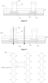
- the present embodiment provides a display panel, as shown in Figure 1 , the display panel comprises a substrate 1, and a first film layer 2 and a second film layer 3 disposed on the substrate 1 in sequence.
- the first film layer 2 has a patterned structure
- the second film layer 3 is a film layer disposed on the first film layer 2. Since the second film layer has a patterned structure, the display panel are provided with a first location A and a second location B different from the first location, the film layers arranged in a thickness direction of the display panel at the first location A are different from the film layers arranged in a thickness direction of the display panel at the second location B, as shown in a path a and a path b in Figure 1 .
- the path a and the path b respectively comprise different film layers.
- the path a comprises the second film layer 3, the first film layer 2, and the substrate 1.
- the path b comprises the second film layer 3 and the substrate 1.
- the path a and the path b meet the following conditions: the substrate 1, the first film layer 2 and the second film layer 3 respectively have film layer coefficients of n 1 , n 2 and n 3 , and the substrate 1 has a thickness of d 1 , the first film layer has a thickness of d 2 , and the second film layer has a thickness of d a in the path a, and the second film layer has a thickness of d b in the path b.
- L L a - L b and L meets meet the following condition: (m-0.2) ⁇ ⁇ L ⁇ (m+0.2) ⁇ , wherein, m is a natural number; ⁇ represents a distance coefficient and has a value between 380nm to 780nm.
- the film layer coefficients n 1 , n 2 and n 3 respectively correspond to the substrate 1, the first film layer 2 and the second film layer 3, and ⁇ is a wavelength of visible light.
- the display panel in this solution has a patterned structure in the film layer thereof; the film layers arranged in a thickness direction of the display panel at the first location A are different from the film layers arranged in a thickness direction of the display panel at the second location B, and the first location A and the second location B correspond to two locations where light passes vertically through the display panel, forming two paths to be passed through by light.
- the thicknesses of the first film layer and the second film layer By reasonably setting the thicknesses of the first film layer and the second film layer and reasonably selecting the film layer coefficients of the first film and the second film layer such that the locations A and B meet the above condition, that is, when light enters the display panel perpendicular to the substrate surface via the path a and the path b, a difference value between the optical lengths of the two paths and the wavelength of light meet the above conditions, and as a result, when light exits the display panel via the path a and the path b, the phase difference thereof is relatively small.
- phase difference generated between light beams with the same initial phase position after passing through the display panel is one of the important reasons for occurrence of diffraction
- the phase difference of the light beams is relatively small and diffraction is weak after light beams with the same initial phase position pass through the display panel via the two different paths, and diffraction phenomenon caused by phase difference is alleviated, so that the above-mentioned image distortion due to diffraction does not occur after light passes through the display panel, which improves the clarity of the image captured by the camera behind the display panel, and enables the photosensitive device behind the display panel to acquire clear and real images, thereby realizing full-screen display.
- the difference value of L a -L b is selected as 0, in other words, the difference value between the optical lengths of the two paths is 0 which is easier to be implemented and operated as compared to an integer multiple of the wavelength of light.
- the number of film layers arranged at the first location and the second location can be determined according to actual needs.
- the film layers arranged in the thickness direction of the display panel at the first location has a total number of i and respective thicknesses of d 1 , d 2 , ... d i ;
- the film layers arranged in the thickness direction of the display panel at the second location has a total number of j and respective thicknesses of D 1 , D 2 , ...
- n 1 , n 2 , ..., n i and N 1 , N 2 , ..., N j have values between 1 and 2, corresponding to the value ranges of respective refractive indices of the film layers in the transparent screen, and the distance coefficient ⁇ corresponds to a wavelength of visible light.
- the light passing through at the first location has an optical path L 1 and the light passing through at the second location has an optical path L 2 , that is, the difference value between the optical lengths of light passing through at the first location and at the second location is L 1 -L 2 .
- a difference value between the optical lengths deviates from an integer multiple of the wavelength by a deviation value within a preset range. After light passes through the panel at the first location and the second location, the phase difference thereof is small, and the diffraction phenomenon incurred is not notable.
- the first location and the second location may also be any locations where light is incident, as long as the film layers arranged in a thickness direction of the display panel at the first location are different from the film layers arranged in a thickness direction of the display panel at the second location.
- the concerned film layer may be multiple film layers, wherein one or more of the film layers have a patterned structure, so that when light passes through the display panel vertically, a plurality of paths are formed. Each of the paths comprises different film layers.
- the difference value between the optical lengths of at least two of the paths to be passed through by light in association with the wavelength of the light meet the above conditions, so that the diffraction phenomenon of light after passing through the at least two paths can be alleviated.
- the diffraction phenomenon of light after passing through the display panel via these paths can be effectively alleviated.
- the diffraction phenomenon caused by light beams passing through the display panel would be weaker.
- the difference value of the optical lengths obtained meets the above correspondence relationship. In this way, the phase difference caused by phase diversity after light passes through the display panel can be eliminated, such that the occurrence of diffraction phenomena can be greatly alleviated.
- the display panel in this embodiment is an AMOLED display panel.
- the display panel comprises a substrate 001, a laminate layer 002, a planarization layer 003, a conductive line 0041, an anode layer 0042, a pixel defining layer 005, a light emitting structure layer 006, and a cathode layer 007.
- the substrate 001 here can be a rigid substrate, e.g. a transparent substrate such as a glass substrate, a quartz substrate or a plastic substrate; the substrate 001 can also be a flexible transparent substrate, such as a polyimide (PI) film, so as to improve the transparency of the device. Since the substrate is the same in all paths through which the light passes vertically, the substrate has no substantial influence on the difference between the optical lengths of different paths to be passed through by light.
- PI polyimide
- a laminate layer 002 is disposed on the substrate 001, and the laminate layer 002 includes pixel circuits. Specifically, it comprises one or more switching devices and capacitors and other devices. A plurality of switching devices are connected in series or in parallel, according to needs, to form a pixel circuit such as 2T1C (2 transistors plus 1 capacitor) and 7T1C (7 transistors plus 1 capacitor), which is not limited herein.
- the switching device can be a thin film transistor (TFT), the thin film transistor can be an oxide thin film transistor or a low temperature polycrystalline silicon thin film transistor (LTPS TFT), and the thin film transistor is preferably an indium gallium zinc oxide thin film transistor (IGZO TFT).
- the switching device can also be a metal-oxide semiconductor field effect transistor (MOSFET), and can also be other components with conventional switching characteristics, such as an insulated gate bipolar transistor (IGBT), etc., as long as the components can implement the switching function in the present embodiment and can be integrated into the display panel, they all fall into the protection scope of the present application.
- MOSFET metal-oxide semiconductor field effect transistor
- IGBT insulated gate bipolar transistor
- a pixel driving circuit comprises a variety of devices, thus forming a multilayer film structure which comprises a source electrode, a drain electrode, a gate electrode, a gate insulating layer, an active layer, an interlayer insulating layer, etc.
- Each film layer is formed with a patterned film layer structure.
- light passes through different pathways, so the optical length of the path through which light passes can be adjusted by adjusting the thickness or refractive index of each film layer in the pixel circuit.
- other film layers can also be adjusted to work together for adjusting the optical length of the path to be passed through by light.
- a planarization layer 003 is disposed on the laminate layer 002, and a flat plane is formed by the planarization layer 003, which is convenient for setting electrodes and conductive lines, etc. thereon. Since the laminate layer 002 has a patterned structure, the thickness of the planarization layer 003 is different at different locations. By adjusting the thicknesses and refractive indices at different locations of the planarization layer, the optical lengths of different paths can be adjusted.
- An anode layer 0042 and a conductive line 0041 are disposed on the planarization layer 003. The anode layer 0042 and the conductive line 0041 in Figure 2 are disposed in the same layer.
- the anode layer 0042 and the conductive line 0041 can be disposed in different layers that are manufactured separately.
- the conductive lines comprise at least one of scan lines, data lines, power lines, and reset lines.
- the scan lines may comprise a SCAN line and an EM line, and the data line is V data , the power line is VDD or VSS, and the reset line is V ref .
- the conductive line may be a single layer or multiple layers of conductive lines disposed on the planarization layer, or the conductive line may be multiple layers of conductive lines spaced apart and having patterns crossing each other.
- the anode layer 0042 and the conductive line 0041 may be made of transparent conductive materials.
- Indium tin oxide (ITO), indium zinc oxide (IZO), or silver-doped oxide, Indium tin oxide (Ag+ITO), or silver-doped indium zinc oxide (Ag+IZO) may be generally used.
- the conductive material is indium zinc oxide, as the manufacturing process of ITO is mature and the cost thereof is low.
- materials such as aluminum-doped zinc oxide, silver-doped ITO, or silver-doped IZO are used as the transparent conductive materials. Both the thickness and the refractive index of the anode layer 0042 and the conductive line 0041 can be adjusted.
- the optical length of the path to be passed through by light can be adjusted, so that the difference value between the optical length of a specific path and the optical length of another path meets the above conditions.
- the thickness thereof 0042 is generally in the range of 20nm to 200nm, and the thickness of the ITO layer can be adjusted within this range.
- the conductive lines 0041 and the anode layer 0042 are prepared separately, their thicknesses and refractive indices can be adjusted separately.
- the thickness and/or refractive index of each layer of conductive line can also be adjusted separately. If they are formed in the same layer, the thickness and refractive index of both the conductive line 0041 and the anode layer 0041 can only be adjusted at the same time.
- the conductive line 0041 and the anode layer 042 are disposed in the same layer.
- the conductive lines 0041 are multiple layers of lines, there may be one layer of conductive line disposed in the same layer as the anode layer, and the line and the anode layer can be made of the same material or different materials.
- the conductive line may also be a double-layer line, for example, the conductive line comprises a first conductive line and a second conductive line.
- the first conductive line is disposed in the same layer as the anode layer, and the second conductive line is disposed between a planarization layer and a substrate.
- the first conductive line and the second conductive line are made of the same material as the first electrode layer (anode layer).
- An encapsulation layer, a second electrode layer (cathode layer), a pixel defining layer, the first conductive line and a substrate form a light path; an encapsulation layer, a second electrode layer, a pixel-defining layer, the second conductive line and a substrate may also form another light path; in a portion where projections of the first conductive line and the second conductive line overlap, an encapsulation layer, the second electrode layer (cathode layer), the pixel-defining layer, the first conductive line, the second conductive line and the substrate may also form still another light path.
- the paths through which light passes through may further include a path comprising an encapsulation layer, a second electrode layer (cathode layer), a light emitting layer, a first electrode layer (anode layer), a second conductive line, and a substrate.
- a pixel defining layer 005 is disposed on the anode layer 0042 to limit the position of the pixels, and pixel openings are formed in the pixel defining layer 005.
- the pixel defining layer 005 has a relatively large thickness to allow for a large adjustable range.
- the pixel defining layer 005 generally has a thickness of 0.3-3 ⁇ m, and the thickness of the pixel defining layer 005 can be adjusted within this range. Therefore, it is preferable to adjust the thickness of the pixel defining layer 005 so that the optical length meets the above conditions.
- the material of the pixel defining layer 005 can be adjusted together, thus adjusting its refractive index; or both the thickness and refractive index of the pixel defining layer 005 may be adjusted at the same time, so as to adjust the optical length of the path to be passed through by light.
- a support layer 0051 is disposed upon the pixel defining layer 005 for supporting a mask during a production process. As shown in Figure 3 , if the support layer 0051 is a transparent structure, for the optical path passing through the support layer 0051, the optical length of the path can also be adjusted by adjusting the thickness and refractive index of the support layer 0051.
- the support layer 0051 can also be provided as an opaque structure, as shown in Figure 4 , if a black opaque structure is used (a black opaque support layer, referred to as a spacer or a SPC), and one or more TFT structures in the pixel circuit set beneath the black support layer 0051 can be shielded by the black opaque structure, so that light does not pass through the plurality of film layer structures in the pixel circuit when it passes through the display panel, therefore, the process of adjusting the optical lengths of different paths is simplified while preventing diffraction phenomenon from being caused by the patterned structure of this part of film layers.
- a black opaque structure a black opaque support layer, referred to as a spacer or a SPC
- Pixel openings are formed in the pixel defining layer 005, and a light emitting structure layer 006 is disposed in each of the pixel openings and upon the pixel defining layer 005.
- An organic light-emitting diode (OLED) is used herein, and the light emitting structure layer 006 generally comprises a light extraction layer, an electron injection layer, an electron transport layer, a hole blocking layer, a light emitting layer, a hole transport layer, and a hole injection layer. All the layers are arranged on the entire surface except for the light-emitting layer, so that all the layers other than the light-emitting layer have no influence on the difference value between optical lengths of the paths to be passed though by light.
- the light-emitting layer is disposed in each of the pixel openings.
- Different light-emitting sub-pixels comprise different light-emitting materials, including red light-emitting materials, blue light-emitting materials, and green light-emitting materials.
- the optical length of the paths to be passed through by light can also be adjusted by adjusting the thickness or refractive index of the light-emitting materials in the light-emitting layer, or adjusting both the thickness and refractive index of the light-emitting materials at the same time.
- the adjustable range thereof is small, and generally, the optical length can be adjusted in cooperation with other film layers, and it is difficult to adjust this layer alone to make the optical length meet the above conditions.
- a cathode layer 007 is disposed on the light emitting structure layer 006. Since the cathode layer is arranged on the entire surface, the cathode layer has no substantial influence on the difference value between the optical lengths of the paths to be passed through by light.
- a light extraction layer 008 can be further disposed on the cathode layer 007, as shown in Figure 5 . The light extraction layer 008 can be omitted in some embodiments.
- An encapsulation layer is disposed on an outer side of the light extraction layer 008.
- the encapsulation layer can be encapsulated with a hard screen encapsulation or an organic thin film encapsulation.
- the display panel in Figure 5 is a hard screen encapsulated with glass powder (i.e., Frit encapsulation), wherein the encapsulation layer comprises a low vacuum gap layer 009 and an encapsulation substrate 010.
- the vacuum gap layer is filled with an inert gas, and the encapsulation substrate is an encapsulation glass.
- the display panel shown in Figure 5 when lights pass through the display panel, a plurality of optical paths can be formed. Since the display panel has two types of light-emitting structures including a top-emitting structure and a bottom-emitting structure. If the display panel has a top-emitting structure, a side to be encapsulated faces outward, the substrate is on an inner side, and the camera is disposed below the substrate. If the display panel has a bottom-emitting structure, a side where the substrate is located faces outward and a side to be encapsulated faces inward, and the camera is disposed below the encapsulation glass.
- the display panel is a transparent display panel, and when a camera disposed below the display panel works, pixels in the camera area do not emit light, so as to allow external light to pass through.
- the paths of light passing through the panel are the same.
- the top-emitting structure is taken as an example for illustration.
- a path A sequentially passes through an encapsulation substrate 010, a vacuum gap layer 009, a light extraction layer 008, a cathode layer 007, a light emitting structure layer 006, an anode layer 0042, a planarization layer 003, a laminate layer 002, and a substrate 001.
- a path B sequentially passes through an encapsulation glass layer 010, a vacuum gap layer 009, a light extraction layer 008, a cathode layer 007, a light emitting structure layer 006, a pixel defining layer 005, a planarization layer 003, a laminate layer 002, and a substrate 001.
- a path C sequentially passes through an encapsulation glass layer 010, a vacuum gap layer 009, a light extraction layer 008, a cathode layer 007, a light emitting structure layer 006, a pixel defining layer 005, a conductive line 0041, a planarization layer 003, a laminate layer 002, and a substrate 001.
- a path D sequentially passes through an encapsulation glass layer 010, a vacuum gap layer 009, a light extraction layer 008, a cathode layer 007, a light emitting structure layer 006, a pixel defining layer 005, an anode layer 0042, a planarization layer 003, a laminate layer 002, and a substrate 001.
- the thickness of the low vacuum gap layer in the path A is larger than the thickness of the low vacuum gap layer in the other paths.
- the optical length of the path A to be passed through by light is L A
- the optical length of the path B to be passed through by light is L B
- the optical length of the path C to be passed through by light is L C .
- the difference value between the optical lengths of the paths A, B, and C is an integer multiple of the wavelength of light.
- L the optical length
- i the number of structural layers in the path through which light passes
- d 1 , d 2 , ..., d i respectively represent the thicknesses of the respective structure layers in the path through which light passes
- n 1 , n 2 , ..., n i respectively represent the refractive indices of the respective structural layers in the path through which light passes.
- the optical length of each path can be calculated.
- each path passes through a plurality of layers, if two paths include the same film layer(s) with identical material and thickness, the difference value between the optical lengths of these two paths will not be affected by this/these same film layer(s) when calculating the difference value between the optical lengths. Only those film layers made of different materials, or those film layers having the same material but having different thicknesses, would affect the difference value between the optical lengths.
- the substrate 001, the encapsulation substrate 010, the light extraction layer 008 and the cathode layer 007 are made of the same materials and have the same thickness, so these layers may not be considered.
- the layers in the path A that are different from those in the path B are the vacuum gap layer 009 (included in both the path A and the path B, but having different thicknesses), the pixel defining layer 005 (included in the path B, but not in the path A), and the anode layer 0042 (included in the path A, but not in the path B).
- the thickness difference between the vacuum gap layer 009 in the path A and the vacuum gap layer 009 in the path B has the same value as the thickness of the pixel defining layer 005 in the path B, if the thickness of the pixel defining layer 005 is adjusted, the thickness difference between the vacuum gap layer 009 in the path A and the vacuum gap layer 009 in the path B will be adjusted accordingly. It can be seen that the path A and path B are mainly affected by the anode layer 0042 and the pixel defining layer 005.
- the difference value between the optical lengths of the path A and the path B can be controlled to deviate from an integer multiple of the wavelength of the light by a deviation value within a preset range.
- the light emitting layer in the light emitting structure layer 006 wherein the light emitting layer in the pixel opening and the light emitting layer outside the pixel opening may be different, and the optical lengths of the paths can be further adjusted by adjusting the light emitting layer.
- the film structures of the planarization layer 003 and the laminate layer 002 in the path A and in the path B can also be different, and the optical lengths can be adjusted by adjusting the thickness and/or the refractive index of these different film layers.
- a black support layer 0051 can also be disposed on top of the switching device of the pixel circuit, so that light does not pass through the pixel circuit, thereby preventing the light from influencing the performance of the pixel circuit, and at the same time preventing light diffraction caused by the existence of various layers of the pixel circuit.
- the path C comprises a conductive line 0041
- the thickness of the pixel defining layer 005 in the path C is different from the thickness of the pixel defining layer 005 in the path B.
- the difference between the thickness of the pixel-defining layer 005 in path C and the thickness of the pixel-defining layer 005 in path B is equal to the thickness of the conductive line 0041. Therefore, by adjusting the thickness and refractive index of the conductive line 0041, the difference value between the optical lengths of the path B and the path C can be made to meet the above requirements.
- the conductive line in the path C can also be double-layer lines including a first conductive line and a second conductive line, wherein the first conductive line is disposed in the same layer as the first electrode layer, the second conductive line is disposed between the planarization layer and the substrate.
- the difference value between the optical lengths can be controlled to deviate from an integer multiple of the wavelength of the externally incident light by a deviation value within a preset range after the externally incident light passes through the path B and the path C respectively, such that the phase difference is relatively small after light passes through these two paths.
- the difference between the path A and the path C lies in the encapsulation layer, the pixel defining layer 005, the anode layer 0042, and the conductive line 0041.
- the thickness of the encapsulation layer is determined by the thickness of the pixel defining layer 005, therefore the thickness or the refractive index of the layer 005 can be adjusted, or both the thickness and the refractive index of the pixel defining layer 005 are adjusted at the same time. If the anode layer 0042 and the conductive line 0041 are arranged in the same layer, the difference value between the optical lengths of the paths A and C will not be substantially affected by the anode layer 0042 and the conductive line 0041.
- the difference value between the optical lengths of the path A and the path C can also be adjusted by adjusting the thickness and/or the refractive index of the anode layer 0042 and the conductive line 0041.
- the difference between path A and path D lies in the encapsulation layer and the pixel defining layer 005.
- the thickness of the encapsulation layer is determined by the thickness of the pixel defining layer 005, so the thickness or the refractive index of the pixel defining layer 005 can be adjusted, or both the thickness and the refractive index of the pixel defining layer 005 can be adjusted at the same time, so as to adjust the difference value between the optical lengths of the paths A and D.
- path B and path D The difference between path B and path D is the pixel defining layer 005 and the anode layer 0042, so the thickness and/or refractive index of the pixel defining layer 005 and the anode layer 0042 can be adjusted to adjust the difference value between the optical lengths of the paths B and D.
- path C and path D lies in the anode layer 0042 and the conductive line 0041. If the anode layer 0042 and the conductive line 0041 are arranged in the same layer, the optical lengths of the path A and the path C are the same, and there is no difference between the optical lengths thereof. If the anode layer 0042 and the conductive line 0041 are arranged in different layers, the difference value between the optical lengths of the path C and the path D can also be adjusted by adjusting the thickness and/or the refractive index of the anode layer 0042 and the conductive line 0041.
- the path B, the path C and the path D can comprise a support layer, and the path B, the path C and the path D may further comprise a TFT structure layer forming a pixel circuit. Since the TFT structure layer comprises a plurality of layers, different layers of the TFT structure will exist in the path B, the path C, and the path D according to the specific structural arrangements. Since the support layer 0051 is disposed on the pixel defining layer 005, the support layer 0051 does not exist in the path A.
- the conductive line in the above embodiment can be a single-layer conductive line or a multilayer conductive line.
- the conductive line is selected from at least one of a scan line, a data line, a power line, and a reset line.
- the scan line may include a SCAN line and an EM line.
- the data line is V data
- the power line is VDD or VSS
- the reset line is V ref .
- the conductive line can also be a double-layer line, for example the double-layer line comprises a first conductive line and a second conductive line, wherein the first conductive line is disposed in the same layer as the anode layer, and the second conductive line is disposed between the planarization layer and the substrate.
- the first conductive line and the second conductive line are made of the same material as the first electrode layer (anode layer), thus, the encapsulation layer, the second electrode layer (cathode layer), the pixel defining layer, the first conductive line and the substrate form an optical path; the encapsulation layer, the second electrode layer (cathode layer), the pixel defining layer, the second conductive line and the substrate can form another optical path; and in a portion where projections of the first conductive line and the second conductive line overlap, the encapsulation layer, the second electrode layer (cathode layer), the pixel defining layer, the first conductive line, the second conductive line and the substrate can form still another optical path.
- the paths through which the light passes may include a path comprising an encapsulation layer, a second electrode layer (cathode layer), a light emitting layer, a first electrode layer (anode layer), a second conductive line, and a substrate.
- the thickness of the anode layer 0042 in the path A and the thickness of the pixel defining layer 005 in the path C are adjusted, so that the optical lengths of the paths A and the path C are the same.
- a thin film encapsulation method can also be adopted.
- an outer side of the light extraction layer 008 is thin-film encapsulated to form a thin-film encapsulation layer.
- the thin-film encapsulation layer comprises an inorganic material encapsulation layer 012 and an organic material encapsulation layer 011, and the inorganic material encapsulation layer 012 is disposed on the entire surface and has a uniform thickness, so the inorganic material encapsulation layer 012 has no effect on the difference value between the optical lengths of the paths.
- the organic material encapsulation layer 011 fills the pixel opening fully.
- the thickness of the organic material encapsulation layer is different. Therefore, the optical lengths of the paths to be passed through by light can be adjusted by adjusting the thickness of the organic material encapsulation layer 011 within the pixel opening, or by adjusting the refractive index of the organic material encapsulation layer, or by adjusting both the thickness and the refractive index of the organic material encapsulation layer at the same time, or by the above means in combination with other adjustment manners.
- the thickness of the organic material encapsulation layer in the path A is greater than the thickness of the organic material encapsulation layer in other paths.
- a plurality of light-transmitting paths can be formed in the display panel when light passes through the display panel.
- the paths may include a path comprising an encapsulation layer, a second electrode layer, a light emitting structure layer, a first electrode layer and a substrate; and/or the paths may include a path comprising an encapsulation layer, a second electrode layer, a light emitting structure layer, a pixel defining layer and a substrate; and/or the paths may include a path comprising an encapsulation layer, a second electrode layer, a light-emitting structure layer, a pixel-defining layer, a conductive line and a substrate.
- one or more difference values between the optical lengths can be controlled to deviate from an integer multiple of the wavelength of the light by a deviation value within a preset range by adjusting the thickness and/or the refractive index of one or more layers selected from the encapsulation layer, the light-emitting structure layer, the first electrode layer, the pixel-defining layer, the insulating layer, and the conductive line.
- the specific adjustment manners have been respectively described in the above embodiments, which will not be repeatedly described herein.
- the shapes of the electrodes in the anode layer, the pixel openings and the conductive line can be adjusted to further alleviate diffraction.
- the anode 300 can be set to have a circular shape as shown in Figure 12 , or an oval shape as shown in Figure 13 , or a dumbbell shape as shown in Figure 14 .
- the anode can also be formed by other types of curves with different curvature radii. When light passes through obstacles such as slits, small holes, or disks, it will bend at different degrees in its transmission direction and deviate from a rectilinear transmission direction.
- This phenomenon is called diffraction.
- the distribution of diffraction fringes is affected by the size of the obstacle, such as the width of the slit and the size of the small hole.
- the diffraction fringes at locations having the same width are consistent, which will cause more notable diffraction effects.
- the sides of a projection of the opening of the pixel defining layer 005 on the substrate are not parallel to each other and each side thereof has a curve shape, that is, the opening has varying widths in all directions and has different diffusion directions of diffraction at the same location.
- diffraction fringes having different positions and diffusion directions can be generated at the locations with different widths, thereby preventing any notable diffraction effect, and ensuring that a photosensitive device disposed below the display panel can work normally.
- the openings in the pixel-defining layer are all set to have a rectangular shape or a square shape according to the pixel size.
- the rectangular shape since the rectangular shape has two sets of parallel sides, the rectangular shape has the same size in both the length direction and the width direction. Therefore, when external light passes through the opening, diffraction fringes having the same position and the same diffusion direction are generated at all the different locations in the length direction or the width direction, thus a significant diffraction effect may occur, making the photosensitive device below the display panel unable to work normally.
- This problem can be well solved by the display panel of the present embodiment which can ensure that the photosensitive device below the display panel can work normally.
- each side of a projection of the opening on the substrate may have a shape selected from at least one of a circular shape, an oval shape and other curves with varying curvature.
- the sides of the opening have a curve shape. Therefore, when light passes through the opening, the diffraction fringes generated will not diffuse only in one direction, but will diffuse in 360-degree directions, which makes the diffraction extremely insignificant and leads to a better diffraction alleviation effect.
- a projection shape unit of the opening on the substrate has a circular shape, an oval shape, a dumbbell shape or a wavy shape, which is similar to the shape of the anode 300, and can refer to the shapes of the anode 300 shown in Figures 12-14 , and which is not repeatedly described herein.
- the shape of the projection of the opening on the substrate can be determined according to the shape of the corresponding light emitting structure. For example, the number of shape units can be determined according to the aspect ratio of the light emitting structure.
- a projection of the opening on the substrate may have an axisymmetric structure, so as to ensure that each pixel on the entire display panel has a uniform aperture ratio and not to affect the final display effect.
- the corresponding light-emitting structure has a rectangular or square shape with an aspect ratio less than 1.5, and the symmetry axis of the projection of the opening corresponds to the symmetry axis of the corresponding light-emitting structure.
- a diameter of the circle of the projection is smaller than the minimum width of the light emitting structure.
- the diameter of the circle of the projection can be determined according to the shape of the light emitting structure in combination with the aperture ratio. Since the method for determining the size of the opening in the related technology can be used in the determination process herein, it is not described herein.
- the pixel opening and the anode electrode can also be eccentric with respect to each other, that is, the circle center of the pixel opening and the circle center of the anode electrode do not coincide.
- the projection of the opening has a dumbbell shape formed by interconnecting two circles to each other.
- the two circles are respectively arranged along a length direction of the corresponding light emitting structure.
- the projection of the opening has a wave shape formed by interconnecting three or more circles with each other.
- the three or more circles are respectively arranged along a length direction of the corresponding light-emitting structure.
- connecting portions are further formed in the projection.
- the connecting portions have an arc shape, that is, the intersections of the three or more circles are interconnected by arcs, so that, when light passes through the connecting portion, it can also be diffused towards different directions, thereby alleviating the diffraction effect.
- the projection of the opening may have a circular shape, or may have a dumbbell shape that are formed by two circles interconnected to each other.
- the projection may have a dumbbell shape formed by two circles interconnected to each other, or may have a wave shape formed by three circles interconnected with each other, as shown in Figure 15 .
- the pixel opening 005 may also have a circular shape, as shown in Figure 16 .
- the display panel can be PMOLED. Since the PMOLED and the AMOLED have different structures, when light passes through PMOLED, there are different paths to be formed.
- the PMOLED comprises a substrate 110, an anode layer 120, a pixel defining layer 130, an isolation pillar 140, a light emitting structure layer 150, and a cathode layer 160.
- the anode layer 120 comprises a plurality of first electrodes, and a plurality of anodes are regularly arranged on the substrate 110.
- a light emitting structure layer 150 is formed on the anode, and a cathode layer 160 is formed on the light emitting structure layer 150.
- the isolation pillar 140 is formed on the pixel defining layer 130 and is disposed between adjacent first electrodes.
- the isolation pillar 140 is used to separate the cathodes of two adjacent sub-pixel regions.
- the isolation pillar 140 has an inverted trapezoidal structure and made of a transparent material, such as transparent photoresist.
- the surface of the isolation pillar 140 is higher than the surface of the regions adjacent to the isolation pillar 140. Therefore, when a cathode is prepared on the surface of the display panel, the cathode formed above the isolation pillar 140 is disconnected from the cathode on the pixel regions adjacent to the isolation pillar 140, thereby realizing separation of the cathodes of adjacent sub-pixel regions, which ultimately ensures that each sub-pixel region can be driven normally.
- the paths through which light passes also include a path comprising the isolation pillars 140.
- the path C comprises the cathode layer 160, the isolation pillar 140, the pixel defining layer 130 and the substrate 110
- the path D comprises the cathode layer 160, the light emitting structure layer 150, the anode layer 120 and the substrate 110.
- different film layers include an isolation pillar 140, a pixel defining layer 130, a light emitting structure layer 150, and an anode layer 120.
- the difference value between the optical lengths of the path C and the path D to be passed through by light can be adjusted.
- the optical length of the path to be passed through by light can be adjusted by adjusting the thickness and/or the refractive index of the layers that are different in the respective paths.
- Other adjustment methods of the paths are the same as those in the foregoing embodiments, and details theerof are not repeatedly described herein.
- the path A, the path B, the path C, and the path D in the above embodiments may also be referred to as a first path, a second path, a third path, a fourth path, and the like.
- the above-mentioned light is visible light
- the wavelength of the light is 380-780 nanometers
- the wavelength of the light is 500-600 nanometers
- human eyes are more sensitive to the light in this preferable range (i.e., green light).
- the incident light can be selected to be based on green light, that is, when adjusting the optical length of each path to be passed through by light, ⁇ can be selected from wavelengths of 500nm to 560nm of green light, such as 540nm, 550nm, 560nm. Since the wavelength of green light is between red light and blue light, the red light and blue light can also be taken into account when green light is selected.
- the inventors further found out by research that, when external light passes through patterns in the display panel area, lateral diffraction may also occur, which causes diffraction fringes and in turn affects the normal operation of photosensitive devices such as cameras.
- the isolation pillar 140 includes a plurality of first type isolation pillars.
- the width of the first type isolation pillars changes continuously or intermittently, wherein said extending direction is parallel to the substrate; and said width is a size of a projection of the first type isolation pillar on the substrate in a direction perpendicular to the extending direction.
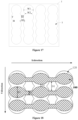
- Figure 10 is a schematic structural view of a first type isolation pillar in an embodiment. In the extending direction of the first type isolation pillars, the width of the first type isolation pillars continuously changes.
- Figure 11 is a top view of a first type isolation pillar in another embodiment, that is, a schematic view of a top surface structure thereof.
- a non-rectilinear shape is formed by connecting the ends of multiple polygonal line segments, thereby ensuring that the first type isolation pillar has varying widths along the extending direction thereof to alleviate the diffraction effect.
- the notches formed by the polygonal line segments are disposed toward the sub-pixel area to reduce the impact on the pixels and ensure that the brightness of the pixels can meet the requirements while ensuring the pixel aperture ratio.
- the polygonal line segments corresponding to each pixel area may also be composed of even more segments, thereby forming a jagged edge.
- both sides in an extending direction of the anode and the cathode in the PMOLED have a wave shape, and the wave crests of the two sides are oppositely disposed and the wave troughs of the two sides are oppositely disposed, as shown in Figure 17 . Further, the wave crests and wave troughs of two adjacent electrodes may be staggered with one another.
- Both the anode and the cathode can have a wavy-striped shape.
- an extending direction of the second electrode 160 and an extending direction of the first electrode 120 are perpendicular to each other, thereby forming a light-emitting area of the display panel in the overlapping area.
- the first electrode 120 is an anode
- the second electrode 160 is a cathode.
- each anode is used to drive one row/column or multiple rows/columns of sub-pixels.
- a pixel (or pixel unit) includes at least three sub-pixels of red, green and blue colors. In other embodiments, one pixel unit may also include four sub-pixels of red, green, blue and white colors.
- the arrangement of the sub-pixels can be a juxtaposed arrangement of RGB sub-pixels, a V-shaped arrangement, or a PenTile arrangement.
- pixel units arranged in juxtaposed arrangement of RGB sub-pixels are taken as an example for illustration. It can be understood that the display panel in this embodiment can also be applied to arrangements other than the juxtaposed RGB sub-pixel arrangement.
- the number of columns/rows of pixels driven by each cathode is M
- the number of columns/rows of pixels driven by each anode is N, wherein M should be greater than or equal to 3 N .
- one pixel unit is constituted by using RBG sub-pixels, and the number of columns/rows of sub-pixels driven by each cathode is M which equals to 3 N .
- the number of column/row of sub-pixels driven by each cathode is M which equals to 4 N . It can be understood that, in other embodiments, the pixels in a column can be driven by the cathode and the pixels in a row can be driven by the anode, wherein the only difference is the different arrangement directions of the anodes and the cathodes.
- Figure 19 is a schematic structural view of cathodes and anodes in a PMOLED display panel according to another embodiment.
- one pixel unit includes three sub-pixels of red, green and blue colors. Therefore, each anode 120 is used to drive a column of pixel units, and each cathode 160 is used to drive a row of sub-pixels.
- the anode pattern can refer to Figure 17 , that is, the width W1 between the oppositely disposed wave crests T is 30 ⁇ m to (A-X) ⁇ m, the width W2 between the oppositely disposed wave troughs B is X ⁇ m to W1, and the minimum distance D1 is (A-W1), the maximum distance D2 is (A-W2).
- X is the minimum process dimension.
- the width W3 between the oppositely disposed wave crests of the two sides of the cathode is X ⁇ m to ((A-X)/3) ⁇ m. It can be understood that, in other embodiments, when the number of sub-pixels in one pixel unit is N, the width W3 between the oppositely disposed wave crests of the two sides of the cathode 160 is X ⁇ m to ((A-X)/N) ⁇ m.
- the width W4 between the oppositely disposed wave troughs of the two sides of the cathode 160 is X ⁇ m to W1, the minimum distance D3 is (A-W3), and the maximum distance D4 is (A-W4), wherein A represents a pixel size and X is a minimum process dimension.
- the distances between adjacent electrodes are all between 4 ⁇ m and 20 ⁇ m.
- the conductive lines are curved in an extending direction thereof; the conductive lines are provided around the first electrodes, and the conductive lines extend in a curve around the edges of the first electrodes, as shown in Figure 20 .
- Both sides of the conductive line in the extending direction thereof have a wave shape, and the wave crests of the two sides are oppositely disposed, and the wave troughs of the two sides are oppositely disposed, as shown in Figure 17 .
- the wirings are designed to extend in a curve in accordance with the size of the pixel electrode, which can further eliminate diffraction as compared to the traditional straight wirings.
- the non-transparent areas can be designed to have a circular shape or an oval shape to alleviate diffraction. Therefore, the opaque support layer 0051 can also be designed to have a circular shape or an oval shape. As shown in Figure 21 , by making the support layer 0051 to have an oval shape, the diffraction can be further alleviated.
- the embodiments of the present application also provide a display screen, as shown in Figure 22 , the display screen comprises a first display area 161 and a second display area 162, the first display area 161 and the second display area 162 are both used to display static or dynamic images, the display panel mentioned in any of the above embodiments is used in the first display area 161, and the first display area 161 is located at an upper part of the display screen.
- the display panel after light passes through the display panel via at least two of the paths, it will not cause phase difference, so that diffraction interference is alleviated. If the phase position do not change after light passes through all the paths in the display panel, diffraction interference caused by the phase difference can be prevented, and the camera below the screen can capture clear and real image information.
- the display screen may comprise three or more display areas, such as three display areas (a first display area, a second display area, and a third display area).
- the display panel mentioned in any of the above embodiments can be used in the first display area, and display panels used in the second display area and the third display area are not limited herein and these display panels can be a PMOLED display panel or an AMOLED display panel, and certainly the display panel of any of the above embodiments can also be used.
- the embodiments of the present application further provide a display apparatus, comprising the above-mentioned display screen overlaid on an apparatus body.
- the display apparatus may be a product or a component having a display function, such as a mobile phone, a tablet PC, a television, a display screen, a palmtop computer, an iPod, a digital camera, a navigator, or the like.
- Figure 23 shows a schematic structural view of a display terminal in an embodiment, the display terminal comprises an apparatus body 810 and a display screen 820.
- the display screen 820 is disposed on the apparatus body 810 and is interconnected with the apparatus body 810.
- the display screen 820 can be the display screen in any of the above embodiments for displaying a static or dynamic picture.
- Figure 24 shows a schematic structural view of an apparatus body 810 in an embodiment.
- the apparatus body 810 can be provided with a slotted area 812 and a non-slotted area 814.
- a photosensitive device such as a camera 930 and a light sensor may be disposed in the slotted area 812.
- the display panel of the first display area of the display screen 820 is attached correspondingly to the slotted area 812 so that the above-mentioned photosensitive device such as the camera 930 and the light sensor can collect external light through the first display area.
- the display panel in the first display area can effectively alleviate the diffraction phenomenon generated by external light passing through the first display area, the quality of the image captured by the camera 930 on the display apparatus can be effectively improved, image distortion of the captured image due to diffraction can be prevented, and the accuracy and sensitivity of the light sensor for sensing external light can also be improved.
Description
- The present application relates to the field of display technologies, and particularly relates to a display panel, a display screen, and a display terminal.
- With rapid development of display terminals, users have an increasingly high level of demands for the screen ratio, such that the full screen display of display terminals has received more and more attention in the industry. Full screens are often routinely slotted or perforated to accommodate elements such as cameras and sensors, for example, bangs screens of Apple iPhones are usually slotted or perforated in a display area corresponding to elements such as cameras and sensors. When the camera is used for photographing, external light goes into the camera below the display screen through the slot or hole in the display screen, so as to realize photographing. However, neither the bangs screen nor the perforated screen is a true full display screen. Therefore, the industry is in urgent need of developing a true full display screen.
- In this respect,
JP 2007 248674 A - In addition,
US 2013/215371 A1 discloses a liquid crystal display element comprising: a first substrate; a second substrate; a liquid crystal layer disposed between the first substrate and the second substrate; a first transparent electrode provided in a display region of the first substrate; and a second transparent electrode provided in a display region of the second substrate, wherein at least one of d1 and d2 is not greater than 60 nm, where d1 represents a thickness of the first transparent electrode and d2 represents a thickness of the second transparent electrode. Thus, a liquid crystal display element and a liquid crystal module in which the occurrence of an interference fringe is prevented are provided. - Further,
EP 1 811 570 A2 - Thus, aimed at solving the above technical problem, the present application provides a display panel as recited in
claim 1. - For this, the present application provides the following technical solutions:
The embodiments of the present application provide a display panel, comprising a substrate, and a plurality of film layers disposed on the substrate in sequence, and at least one of the film layers having a patterned structure, wherein the display panel has at least a first location and a second location different from the first location, and the film layers arranged in a thickness direction of the display panel at the first location are different from the film layers arranged in a thickness direction of the display panel at the second location, the film layers arranged in the thickness direction of the display panel at the first location has a total number of i and respective thicknesses of di, d2, ... di; the film layers disposed arranged in the thickness direction of the display panel at the second location has a total number of j and respective thicknesses of D1, D2, ... Di; i and j are natural numbers, wherein a first optical length L1 at the first location and a second optical length L2 at the second location meet the following conditions:


- According to the invention, λ represents a wavelength of visible light, n1, n2, ..., ni and N1, N2, ..., Nj represent refractive indices of the corresponding film layers at the wavelength of visible light. Optionally, L1-L2 has a value of 0.
- According to the invention, the display panel is an active matrix organic light emitting diode (AMOLED) display panel or a passive matrix organic light emitting diode (PMOLED) display panel, and the film layers include an encapsulation layer, a second electrode layer, a light emitting layer, a first electrode layer, and a pixel defining layer; the film layers arranged in the thickness direction of the display panel at the first location form a first path, and the film layers arranged in the thickness direction of the display panel at the second location form a second path or a third path, wherein, the first path comprises the encapsulation layer, the second electrode layer, the light emitting layer, the first electrode layer, and the substrate; the second path comprises the encapsulation layer, the second electrode layer, the pixel defining layer, the first electrode layer, and the substrate; and the third path comprises the encapsulation layer, the second electrode layer, the pixel defining layer, and the substrate.
- Optionally, the display panel is a film-encapsulated flexible screen, the encapsulation layer comprises a thin film encapsulation layer, the thin film encapsulation layer comprises an organic material encapsulation layer, and the thickness of the organic material encapsulation layer in the first path is greater than the thickness of the organic material encapsulation layer in other paths. Optionally, the display panel is a hard screen encapsulated with glass powder, the encapsulation layer comprises a vacuum gap layer and an encapsulation substrate, and the thickness of the vacuum gap layer in the first path is greater than the thickness of the vacuum gap layer in other paths.
- Optionally, λ has a value range of 500nm-600nm, preferably 550nm.
- Optionally, the display panel is an active matrix organic light emitting diode (AMOLED) display panel, and the film layers further comprise a conductive line, the conductive line is a single-layer line or a multilayer line, and the conductive line includes at least one of a scanning line, a data line, a power line, and a reset line; the film layers arranged in the thickness direction of the display panel at the first location or the second location also form a fourth path comprising the encapsulation layer, the second electrode layer, the pixel defining layer, the conductive line and the substrate.
- Optionally, the conductive line is a single-layer line, the conductive line is disposed in the same layer as the first electrode layer, and the conductive line and the first electrode layer are made of the same material, and the fourth path and the second path comprise the same film layers with the same thicknesses; or the conductive line is a multilayer line, and at least one layer of the multilayer line is disposed in the same layer as the first electrode layer, and the conductive line and the first electrode layer are made of the same material or different materials.
- Optionally, the conductive line is a double-layer line comprising a first conductive line and a second conductive line, the first conductive line is disposed in the same layer as the first electrode layer, and the film layers further include a planarization layer, and the second conductive line is disposed between the planarization layer and the substrate, and the first conductive line and the second conductive line are made of the same material as the first electrode layer, and the fourth path comprises the encapsulation layer, the second electrode layer, the pixel defining layer, the first conductive line and/or the second conductive line, and the substrate.
- Optionally, when a projection of the conductive line on the substrate partially overlaps a projection of the first electrode layer on the substrate, a fifth path comprising the encapsulation layer, the second electrode layer, the light emitting layer, the first electrode layer, the second conductive line and the substrate is further provided.
- Optionally, the display panel is an active matrix organic light emitting diode (AMOLED) display panel, and the film layers further comprise a support layer disposed on the pixel defining layer and a thin film transistor (TFT) structure layer for making a pixel circuit, and the support layer is a transparent structure, and at least one of the second path, the third path and the fourth path further comprises the support layer and/or the thin film transistor structure layer.
- Optionally, the display panel is an active matrix organic light emitting diode (AMOLED) display panel, and the film layers further comprise a support layer disposed on the pixel defining layer and a thin film transistor structure layer for making a pixel circuit, and the support layer is an opaque structure, and the thin film transistor structure layer is disposed beneath the support layer. Optionally, the display panel is an AMOLED display panel, and the first electrode has a circular shape, an oval shape or a dumbbell shape.
- Optionally, pixel openings are formed in the pixel defining layer, the pixel openings comprise a first type of pixel openings; and each side of a projection of each of the first type of pixel openings on the substrate has a curved shape and is not parallel to each other.
- Optionally, a projection of each of the first type of pixel openings on the substrate is an image unit or a plurality of image units interconnected with each other; the image unit(s) has/have a circular or oval shape.
- Optionally, the conductive line is curvilinear in an extending direction thereof; the conductive line is provided around the first electrode, and the conductive line extends in a curve around an edge of the first electrode.
- Optionally, both sides of the conductive line in an extending direction thereof have a wave shape, wave crests of the two sides are oppositely disposed, and wave troughs of the two sides are oppositely disposed.
- Optionally, the display panel is a passive matrix organic light emitting diode (PMOLED) display panel, and the film layers further comprise an isolation pillar disposed on the pixel defining layer, and the a sixth path comprising the second electrode layer, the isolation pillar, the pixel defining layer and the substrate is also provided, and the isolation pillar is made of transparent material. Optionally, the isolation pillar comprises a plurality of first type isolation pillars; and the width of the first type isolation pillar changes continuously or intermittently in an extending direction thereof parallel to the substrate; and the width refers to a dimension of a projection of the first type isolation pillar on the substrate in a direction perpendicular to the extending direction. Optionally, the display panel is a passive matrix organic light emitting diode (PMOLED) display panel, and both sides of the first electrode or the second electrode in an extending direction thereof have a wave shape, wave crests of the two sides are oppositely disposed, and wave troughs of the two sides are oppositely disposed; preferably, wave crests and wave troughs of adjacent first electrodes or adjacent second electrodes are staggered with one another.
- Optionally, the film layers further comprise a conductive line, and the conductive line is a single-layer line or a multilayer line, and the conductive line comprises at least one of a scanning line, a data line, a power line, and a reset line.
- Optionally, when the conductive line is a single-layer line, the conductive line is disposed in the same layer as the first electrode layer; or when the conductive line is a multilayer line, at least one layer of the conductive line is disposed in the same layer as the first electrode layer, and the conductive line and the first electrode layer are made of the same material or different materials. Optionally, when a projection of the conductive line on the substrate partially overlaps a projection of the first electrode layer on the substrate, the film layers arranged in the thickness direction of the display panel at the first location or the second location also form a seventh path comprising the encapsulation layer, the second electrode layer, the light emitting layer, the first electrode layer, the conductive line and the substrate.
- Optionally, for the first location and the second location, the thickness and/or the refractive indices of one or more film layers having differences at the first position and the second position can be adjusted, so that the first position and the second position can meet the above conditions.
- The embodiments of the present application further provide a display screen, comprising at least one display area, the at least one display area comprising a first display area, and a photosensitive device being disposed below the first display area; wherein the display panel according to any embodiment of the present application is disposed in the first display area, and every display area of the at least one display area is used to display a dynamic or static image.
- Optionally, the at least one display area further comprises a second display area; the display panel provided in the first display area is a passive matrix organic light emitting diode (PMOLED) display panel or an active matrix organic light emitting diode (AMOLED) display panel, and the display panel provided in the second display area is an active matrix organic light emitting diode (AMOLED) display panel.
- The embodiments of the present application also provide a display terminal, comprising an apparatus body, having a device area; and the display screen according to any of the above embodiments, covering the apparatus body; wherein the device area is located below the first display area and provided with a photosensitive device for collecting light through the first display area.
- Optionally, the device area is a slotted area, and the photosensitive device comprises a camera and/or a light sensor.
- The technical solutions of this application have the following advantages:
- (1) In the display panel provided in the embodiments of the present application, the film layers have a patterned structure, and the display panel has at least a first location and a second location different from the first location, and the first location and the second location meet the following condition: (m-0.2)λ < L1-L2 < (m+0.2)λ. Since the first location and the second location meet the above condition, when light exits the display panel after going through a first path and a second path, the phase difference of the light beams is relatively small. Since a phase difference generated between light beams with the same initial phase position after passing through the display panel is one of the important reasons for occurrence of diffraction, in the technical solution of the present application, after the light beams with the same initial phase position pass through the display panel via the first path and the second path, the phase difference thereof is within a preset range such that the diffraction phenomenon caused by phase difference is alleviated, so that image distortion due to the above-mentioned diffraction is relatively less after light passes through the display panel, which improves the clarity of the image captured by a camera behind the display panel, and enables a photosensitive device behind the display panel to acquire clear and real images, thereby realizing full-screen display.
- (2) In the display panel provided in the embodiments of the present application, the first location and the second location correspond to locations where incident light enters each path. There are multiple paths for light beams to pass through the display panel, and the number of paths is determined according to the types of paths of the display panel to be passed through by light beams that are vertical to the display panel, and different paths comprise different film layers. When there are multiple paths, the difference value between the optical lengths formed by incident light passing through two of the multiple paths deviates from an integer multiple of the wavelength of the incident light by a deviation value which is in a preset range, such that diffraction caused by light beams passing through the display panel via these paths can be effectively alleviated. When there are more paths meeting such condition, the diffraction phenomenon caused by light beams passing through the display panel would be weaker. As a preferred solution, the difference value between the optical lengths formed by light beams passing through any two of the multiple paths deviates from an integer multiple of the wavelength of the incident light by a deviation value within the preset range. In this way, the phase difference caused by phase diversity after light passes through the display panel can be eliminated, therefore, the diffraction phenomena can be greatly alleviated.
- (3) The display panel in the embodiments of the present application can be a passive matrix organic light emitting diode (PMOLED) or an active matrix organic light emitting diode (AMOLED). There are different paths when light passes through the display panel according to different film layer structures of the display panel. By adjusting the thickness and/or refractive index of one of the film layers in a specific path, the difference value between an optical length of light passing through this specific path and the optical length(s) of another path or other paths can be made to meet the above condition, wherein the thickness of the film layer can be adjusted according to practical needs, and if the thickness can't be adjusted under the condition of meeting performance requirements, the material of the film layer can be adjusted instead, thereby changing the refractive index of the film layer, which can also achieve the above purpose.
- (4) In the display panel in the embodiments of the present application, the thickness of the pixel defining layer or the thickness of the electrode layer(s) can be preferentially adjusted, and because the thickness of the pixel defining layer is larger than that of other film layers and the thickness thereof is easy to be adjusted, the optical length of a path to be passed through by light can be adjusted preferentially by adjusting the thickness of the pixel defining layer under the condition of meeting performance requirements. In addition, the material of the pixel defining layer can also be adjusted to change the refractive index of the pixel defining layer, and the optical length of a path to be passed through by light can be adjusted by adjusting the refractive index of the pixel defining layer, so that the diffraction phenomenon caused by light passing through the display panel can be alleviated.
- (5) The embodiments of the present application further provide a display screen, and a display terminal having the display screen, equipped with the display panel of any of the above embodiments, wherein a photosensitive device such as a camera or a light sensor is disposed below the display panel, and because the display panel can better alleviate diffraction, the camera and the light sensor can capture more real incident light.
- In order to more clearly illustrate the specific embodiments of the present application or the technical solutions in prior art, the drawings used for describing the specific embodiments or the prior art will be briefly introduced below. Apparently, the appended drawings referred to in the following description only represent some embodiments of the present application, and a person skilled in the art can obtain other drawings based on these drawings without expenditure of creative labor.
-
Figure 1 is a structural view showing a display panel in an embodiment of the present application. -
Figure 2 is a structural view showing a display panel in another embodiment of the present application. -
Figure 3 is a structural view showing a display panel in another embodiment of the present application, in which asupport layer 0051 is disposed upon thepixel defining layer 005 for supporting a mask during a production process with respect to the embodiment ofFigure 2 . -
Figure 4 is a structural view showing a display panel in another embodiment of the present application, in which thesupport layer 0051 is provided as an opaque structure. -
Figure 5 is a structural view showing a display panel in another embodiment of the present application, in which acathode layer 007 is disposed on the light emittingstructure layer 006 and alight extraction layer 008 can be further disposed on thecathode layer 007. -
Figure 6 is a structural view of light passing through a display panel in another embodiment of the present application, which is an embodiment of the invention. -
Figure 7 is a structural view of a display panel in another embodiment of the present application. -
Figure 8 is a schematic structural view of a cathode of a display panel in an embodiment of the present application. -
Figure 9 is a schematic structural view of light passing through a cathode in an embodiment of the present application. -
Figure 10 is a top view of a first type isolation column in an embodiment of the present application. -
Figure 11 is a top view of a first type isolation column in another embodiment of the present application. -
Figure 12 is a top view of anodes in an AMOLED display panel in an embodiment of the present application. -
Figure 13 is a top view of anodes in an AMOLED display panel in another embodiment of the present application, with shape of anodes different from that ofFigure 12 . -
Figure 14 is a top view of anodes in an AMOLED display panel in another embodiment of the present application, with shape of anodes different from that ofFigure 12 . -
Figure 15 is a top view of a projection of openings in a pixel-defining layer in an embodiment of the present application. -
Figure 16 is a top view of a projection of openings of a pixel defining layer and anodes in another embodiment of the present application. -
Figure 17 is a top view of an electrode pattern of a PMOLED display panel in an embodiment of the present application. -
Figure 18 is a top view of patterns of anodes and cathodes of a PMOLED display panel in an embodiment of the present application. -
Figure 19 is a top view of patterns of cathodes and anodes of a PMOLED display panel in another embodiment of the present application. -
Figure 20 is a top view of a conductive wire extending in a curve around the edge of the first electrode in an embodiment of the present application. -
Figure 21 is a top view of an opaque support layer arranged in an oval shape in an embodiment of the present application. -
Figure 22 is a structural schematic view of a display screen in an embodiment of the present application. -
Figure 23 is a schematic view of a terminal structure in an embodiment of the present application; Figure -
Figure 24 is a schematic view of an apparatus body according to an embodiment of the present application. - In the description of the present application, it should be understood that the terms "center", "transverse", "upper", "lower", "left", "right", "vertical", "horizontal", "top", "bottom", "inside" and "outside" indicate orientation or positional relationship which are based on the orientation or positional relationship shown in the drawings, and it is merely for convenience of describing the present application and simplifying the description, rather than indicating or implying that the indicated device or element must have a particular orientation or must be constructed and operated in a particular orientation. Therefore, these terms should not be understood as limiting the scope of the present application. In addition, it should be noted that, when an element is referred to as "formed on another element", the element can be directly connected to the another element or an intermediate element may be present at the same time. When an element is considered as being "connected" to another element, it can be directly connected to the another element, or an intermediate element may be present at the same time. In contrast, when an element is referred to as being "directly on" another element, there is no intermediate element.
- As described in the background part, the so-called full display screen in prior art is not a true full display screen. However, during the research, it was found that if the display panel directly covers on a photosensitive device such as a camera, the display panel located above the photosensitive device such as the camera is required to have a high light transmittance. However, it was further discovered by the inventors that, when a photosensitive device such as a camera is disposed below a transparent display panel, the photographed photos are blurred. Further, the inventors found out that the reason for this problem is that there are patterned film layer structures in the display screen, and when external light pass through these patterned film layer structures, diffraction of light will occur, resulting in blurred photos.
- Furthermore, the inventors also found out that, different sectional structures are formed in the area comprising the patterned film layers and the area without the patterned film layers, so when light enters the display screen and reaches the photosensitive device, the optical paths passed through by the light beams are different. When light passes through different areas of the transparent screen, there is a difference value between the optical lengths of light beams due to differences in the refractive indices and thicknesses of the different film layer structures. When light passes through these different areas, the light beams having the same initial phase position originally will generate a phase difference. The phase difference is one of the important reasons for occurrence of diffraction, and the phase difference will cause significant diffraction phenomena, which will cause diffraction fringes after light passes through the display panel, making the picture distorted and blurred.
- In addition, due to the pixel openings, electrodes, conductive line wiring, etc. in the display screen of electronic devices, external light will have relatively complicated diffraction intensity distribution when passing through edges of these areas, thereby resulting in diffraction fringes, which in turn adversely affects normal working of the photosensitive device such as a camera. For example, when the camera located below the transparent display area works, notable diffraction occurs when external light passes through the conductive line wiring, electrode edges or pixel opening edges in the display screen, such that the picture taken by the camera is distorted.
- The present embodiment provides a display panel, as shown in
Figure 1 , the display panel comprises asubstrate 1, and afirst film layer 2 and asecond film layer 3 disposed on thesubstrate 1 in sequence. Thefirst film layer 2 has a patterned structure, and thesecond film layer 3 is a film layer disposed on thefirst film layer 2. Since the second film layer has a patterned structure, the display panel are provided with a first location A and a second location B different from the first location, the film layers arranged in a thickness direction of the display panel at the first location A are different from the film layers arranged in a thickness direction of the display panel at the second location B, as shown in a path a and a path b inFigure 1 . In the present embodiment, the path a and the path b respectively comprise different film layers. The path a comprises thesecond film layer 3, thefirst film layer 2, and thesubstrate 1. The path b comprises thesecond film layer 3 and thesubstrate 1. The path a and the path b meet the following conditions: thesubstrate 1, thefirst film layer 2 and thesecond film layer 3 respectively have film layer coefficients of n1 , n2 and n3 , and thesubstrate 1 has a thickness of d1 , the first film layer has a thickness of d2 , and the second film layer has a thickness of da in the path a, and the second film layer has a thickness of db in the path b. In this embodiment, d2 + da = d b, and La=n1×d1+n2×d2+n3×da ; Lb=n1×d1+n3×db . L=La -Lb and L meets meet the following condition: (m-0.2)λ < L < (m+0.2)λ, wherein, m is a natural number; λ represents a distance coefficient and has a value between 380nm to 780nm. - In this embodiment, the film layer coefficients n1 , n2 and n3 respectively correspond to the
substrate 1, thefirst film layer 2 and thesecond film layer 3, and λ is a wavelength of visible light. The display panel in this solution has a patterned structure in the film layer thereof; the film layers arranged in a thickness direction of the display panel at the first location A are different from the film layers arranged in a thickness direction of the display panel at the second location B, and the first location A and the second location B correspond to two locations where light passes vertically through the display panel, forming two paths to be passed through by light. By reasonably setting the thicknesses of the first film layer and the second film layer and reasonably selecting the film layer coefficients of the first film and the second film layer such that the locations A and B meet the above condition, that is, when light enters the display panel perpendicular to the substrate surface via the path a and the path b, a difference value between the optical lengths of the two paths and the wavelength of light meet the above conditions, and as a result, when light exits the display panel via the path a and the path b, the phase difference thereof is relatively small. Since a phase difference generated between light beams with the same initial phase position after passing through the display panel is one of the important reasons for occurrence of diffraction, when using the technical solution of the present embodiment, the phase difference of the light beams is relatively small and diffraction is weak after light beams with the same initial phase position pass through the display panel via the two different paths, and diffraction phenomenon caused by phase difference is alleviated, so that the above-mentioned image distortion due to diffraction does not occur after light passes through the display panel, which improves the clarity of the image captured by the camera behind the display panel, and enables the photosensitive device behind the display panel to acquire clear and real images, thereby realizing full-screen display. - In some specific embodiments, the difference value of La-Lb is selected as 0, in other words, the difference value between the optical lengths of the two paths is 0 which is easier to be implemented and operated as compared to an integer multiple of the wavelength of light.
- In other alternative embodiments, the number of film layers arranged at the first location and the second location can be determined according to actual needs. For example, the film layers arranged in the thickness direction of the display panel at the first location has a total number of i and respective thicknesses of d1 , d2 , ... di ; the film layers arranged in the thickness direction of the display panel at the second location has a total number of j and respective thicknesses of D1 , D2 , ...
- Di ; i and j are natural numbers, wherein a first optical length L1 at the first location and a second optical length L2 at the second location meet the following conditions:


- The first location and the second location may also be any locations where light is incident, as long as the film layers arranged in a thickness direction of the display panel at the first location are different from the film layers arranged in a thickness direction of the display panel at the second location. In other embodiments, the concerned film layer may be multiple film layers, wherein one or more of the film layers have a patterned structure, so that when light passes through the display panel vertically, a plurality of paths are formed. Each of the paths comprises different film layers. The difference value between the optical lengths of at least two of the paths to be passed through by light in association with the wavelength of the light meet the above conditions, so that the diffraction phenomenon of light after passing through the at least two paths can be alleviated. The diffraction phenomenon of light after passing through the display panel via these paths can be effectively alleviated. When there are more paths meeting such condition, the diffraction phenomenon caused by light beams passing through the display panel would be weaker. As a further preferred solution, when externally incident light enters the display panel in a direction orthogonal to the surface of the substrate and passes through any two of the several paths, the difference value of the optical lengths obtained meets the above correspondence relationship. In this way, the phase difference caused by phase diversity after light passes through the display panel can be eliminated, such that the occurrence of diffraction phenomena can be greatly alleviated. As a specific embodiment, the display panel in this embodiment is an AMOLED display panel. As shown in
Figure 2 , the display panel comprises asubstrate 001, alaminate layer 002, aplanarization layer 003, aconductive line 0041, ananode layer 0042, apixel defining layer 005, a light emittingstructure layer 006, and acathode layer 007. - The
substrate 001 here can be a rigid substrate, e.g. a transparent substrate such as a glass substrate, a quartz substrate or a plastic substrate; thesubstrate 001 can also be a flexible transparent substrate, such as a polyimide (PI) film, so as to improve the transparency of the device. Since the substrate is the same in all paths through which the light passes vertically, the substrate has no substantial influence on the difference between the optical lengths of different paths to be passed through by light. - A
laminate layer 002 is disposed on thesubstrate 001, and thelaminate layer 002 includes pixel circuits. Specifically, it comprises one or more switching devices and capacitors and other devices. A plurality of switching devices are connected in series or in parallel, according to needs, to form a pixel circuit such as 2T1C (2 transistors plus 1 capacitor) and 7T1C (7 transistors plus 1 capacitor), which is not limited herein. The switching device can be a thin film transistor (TFT), the thin film transistor can be an oxide thin film transistor or a low temperature polycrystalline silicon thin film transistor (LTPS TFT), and the thin film transistor is preferably an indium gallium zinc oxide thin film transistor (IGZO TFT). In another alternative embodiment, the switching device can also be a metal-oxide semiconductor field effect transistor (MOSFET), and can also be other components with conventional switching characteristics, such as an insulated gate bipolar transistor (IGBT), etc., as long as the components can implement the switching function in the present embodiment and can be integrated into the display panel, they all fall into the protection scope of the present application. - A pixel driving circuit comprises a variety of devices, thus forming a multilayer film structure which comprises a source electrode, a drain electrode, a gate electrode, a gate insulating layer, an active layer, an interlayer insulating layer, etc. Each film layer is formed with a patterned film layer structure. In different paths, light passes through different pathways, so the optical length of the path through which light passes can be adjusted by adjusting the thickness or refractive index of each film layer in the pixel circuit. In addition to adjusting the film layers of each path within the
laminate layer 002, other film layers can also be adjusted to work together for adjusting the optical length of the path to be passed through by light. - A
planarization layer 003 is disposed on thelaminate layer 002, and a flat plane is formed by theplanarization layer 003, which is convenient for setting electrodes and conductive lines, etc. thereon. Since thelaminate layer 002 has a patterned structure, the thickness of theplanarization layer 003 is different at different locations. By adjusting the thicknesses and refractive indices at different locations of the planarization layer, the optical lengths of different paths can be adjusted. Ananode layer 0042 and aconductive line 0041 are disposed on theplanarization layer 003. Theanode layer 0042 and theconductive line 0041 inFigure 2 are disposed in the same layer. In other embodiments, theanode layer 0042 and theconductive line 0041 can be disposed in different layers that are manufactured separately. The conductive lines comprise at least one of scan lines, data lines, power lines, and reset lines. The scan lines may comprise a SCAN line and an EM line, and the data line is Vdata, the power line is VDD or VSS, and the reset line is Vref. The conductive line may be a single layer or multiple layers of conductive lines disposed on the planarization layer, or the conductive line may be multiple layers of conductive lines spaced apart and having patterns crossing each other. Theanode layer 0042 and theconductive line 0041 may be made of transparent conductive materials. Indium tin oxide (ITO), indium zinc oxide (IZO), or silver-doped oxide, Indium tin oxide (Ag+ITO), or silver-doped indium zinc oxide (Ag+IZO) may be generally used. Preferably, the conductive material is indium zinc oxide, as the manufacturing process of ITO is mature and the cost thereof is low. Furthermore, in order to reduce the resistance of each conductive line while ensuring high light transmittance, materials such as aluminum-doped zinc oxide, silver-doped ITO, or silver-doped IZO are used as the transparent conductive materials. Both the thickness and the refractive index of theanode layer 0042 and theconductive line 0041 can be adjusted. By adjusting the thickness or adjusting the refractive index or adjusting both the thickness and the refractive index at the same time, the optical length of the path to be passed through by light can be adjusted, so that the difference value between the optical length of a specific path and the optical length of another path meets the above conditions. When theanode layer 0042 is made of ITO, thethickness thereof 0042 is generally in the range of 20nm to 200nm, and the thickness of the ITO layer can be adjusted within this range. When theconductive lines 0041 and theanode layer 0042 are prepared separately, their thicknesses and refractive indices can be adjusted separately. If the conductive lines have a multilayer structure, the thickness and/or refractive index of each layer of conductive line can also be adjusted separately. If they are formed in the same layer, the thickness and refractive index of both theconductive line 0041 and theanode layer 0041 can only be adjusted at the same time. - In the present embodiment, the
conductive line 0041 and the anode layer 042 are disposed in the same layer. In other embodiments, when theconductive lines 0041 are multiple layers of lines, there may be one layer of conductive line disposed in the same layer as the anode layer, and the line and the anode layer can be made of the same material or different materials. - In other embodiments, the conductive line may also be a double-layer line, for example, the conductive line comprises a first conductive line and a second conductive line. The first conductive line is disposed in the same layer as the anode layer, and the second conductive line is disposed between a planarization layer and a substrate. The first conductive line and the second conductive line are made of the same material as the first electrode layer (anode layer). An encapsulation layer, a second electrode layer (cathode layer), a pixel defining layer, the first conductive line and a substrate form a light path; an encapsulation layer, a second electrode layer, a pixel-defining layer, the second conductive line and a substrate may also form another light path; in a portion where projections of the first conductive line and the second conductive line overlap, an encapsulation layer, the second electrode layer (cathode layer), the pixel-defining layer, the first conductive line, the second conductive line and the substrate may also form still another light path.
- In a specific embodiment, when a projection of the conductive line on the substrate overlaps with a projection of the first electrode layer (anode layer) on the substrate, the paths through which light passes through may further include a path comprising an encapsulation layer, a second electrode layer (cathode layer), a light emitting layer, a first electrode layer (anode layer), a second conductive line, and a substrate.
- A
pixel defining layer 005 is disposed on theanode layer 0042 to limit the position of the pixels, and pixel openings are formed in thepixel defining layer 005. Thepixel defining layer 005 has a relatively large thickness to allow for a large adjustable range. Thepixel defining layer 005 generally has a thickness of 0.3-3µm, and the thickness of thepixel defining layer 005 can be adjusted within this range. Therefore, it is preferable to adjust the thickness of thepixel defining layer 005 so that the optical length meets the above conditions. If adjusting the thickness of thepixel defining layer 005 alone cannot meet the requirements, the material of thepixel defining layer 005 can be adjusted together, thus adjusting its refractive index; or both the thickness and refractive index of thepixel defining layer 005 may be adjusted at the same time, so as to adjust the optical length of the path to be passed through by light. - In some embodiments, a
support layer 0051 is disposed upon thepixel defining layer 005 for supporting a mask during a production process. As shown inFigure 3 , if thesupport layer 0051 is a transparent structure, for the optical path passing through thesupport layer 0051, the optical length of the path can also be adjusted by adjusting the thickness and refractive index of thesupport layer 0051. Since the pixel driving circuit structure in thelaminate layer 002 is relatively more complicated and the adjustment of each film layer therein is also relatively more complicated, thesupport layer 0051 can also be provided as an opaque structure, as shown inFigure 4 , if a black opaque structure is used (a black opaque support layer, referred to as a spacer or a SPC), and one or more TFT structures in the pixel circuit set beneath theblack support layer 0051 can be shielded by the black opaque structure, so that light does not pass through the plurality of film layer structures in the pixel circuit when it passes through the display panel, therefore, the process of adjusting the optical lengths of different paths is simplified while preventing diffraction phenomenon from being caused by the patterned structure of this part of film layers. - Pixel openings are formed in the
pixel defining layer 005, and a light emittingstructure layer 006 is disposed in each of the pixel openings and upon thepixel defining layer 005. An organic light-emitting diode (OLED) is used herein, and the light emittingstructure layer 006 generally comprises a light extraction layer, an electron injection layer, an electron transport layer, a hole blocking layer, a light emitting layer, a hole transport layer, and a hole injection layer. All the layers are arranged on the entire surface except for the light-emitting layer, so that all the layers other than the light-emitting layer have no influence on the difference value between optical lengths of the paths to be passed though by light. The light-emitting layer is disposed in each of the pixel openings. Different light-emitting sub-pixels comprise different light-emitting materials, including red light-emitting materials, blue light-emitting materials, and green light-emitting materials. As to different light-emitting sub-pixels, the optical length of the paths to be passed through by light can also be adjusted by adjusting the thickness or refractive index of the light-emitting materials in the light-emitting layer, or adjusting both the thickness and refractive index of the light-emitting materials at the same time. - Because the overall thickness of the light emitting structure layer is small, the adjustable range thereof is small, and generally, the optical length can be adjusted in cooperation with other film layers, and it is difficult to adjust this layer alone to make the optical length meet the above conditions.
- A
cathode layer 007 is disposed on the light emittingstructure layer 006. Since the cathode layer is arranged on the entire surface, the cathode layer has no substantial influence on the difference value between the optical lengths of the paths to be passed through by light. Alight extraction layer 008 can be further disposed on thecathode layer 007, as shown inFigure 5 . Thelight extraction layer 008 can be omitted in some embodiments. - An encapsulation layer is disposed on an outer side of the
light extraction layer 008. The encapsulation layer can be encapsulated with a hard screen encapsulation or an organic thin film encapsulation. The display panel inFigure 5 is a hard screen encapsulated with glass powder (i.e., Frit encapsulation), wherein the encapsulation layer comprises a lowvacuum gap layer 009 and anencapsulation substrate 010. The vacuum gap layer is filled with an inert gas, and the encapsulation substrate is an encapsulation glass. - In the display panel shown in
Figure 5 , when lights pass through the display panel, a plurality of optical paths can be formed. Since the display panel has two types of light-emitting structures including a top-emitting structure and a bottom-emitting structure. If the display panel has a top-emitting structure, a side to be encapsulated faces outward, the substrate is on an inner side, and the camera is disposed below the substrate. If the display panel has a bottom-emitting structure, a side where the substrate is located faces outward and a side to be encapsulated faces inward, and the camera is disposed below the encapsulation glass. The display panel is a transparent display panel, and when a camera disposed below the display panel works, pixels in the camera area do not emit light, so as to allow external light to pass through. - Regardless whether the panel is a top-emitting structure or a bottom-emitting structure, the paths of light passing through the panel are the same. The top-emitting structure is taken as an example for illustration. Light enters the display screen from the side of the
encapsulation glass 010, and as the light pass through the display panel, various paths are formed, as shown inFigure 6 , which represents an embodiment of the invention. - A path A sequentially passes through an
encapsulation substrate 010, avacuum gap layer 009, alight extraction layer 008, acathode layer 007, a light emittingstructure layer 006, ananode layer 0042, aplanarization layer 003, alaminate layer 002, and asubstrate 001. - A path B sequentially passes through an
encapsulation glass layer 010, avacuum gap layer 009, alight extraction layer 008, acathode layer 007, a light emittingstructure layer 006, apixel defining layer 005, aplanarization layer 003, alaminate layer 002, and asubstrate 001. - A path C sequentially passes through an
encapsulation glass layer 010, avacuum gap layer 009, alight extraction layer 008, acathode layer 007, a light emittingstructure layer 006, apixel defining layer 005, aconductive line 0041, aplanarization layer 003, alaminate layer 002, and asubstrate 001. - A path D sequentially passes through an
encapsulation glass layer 010, avacuum gap layer 009, alight extraction layer 008, acathode layer 007, a light emittingstructure layer 006, apixel defining layer 005, ananode layer 0042, aplanarization layer 003, alaminate layer 002, and asubstrate 001. - The thickness of the low vacuum gap layer in the path A is larger than the thickness of the low vacuum gap layer in the other paths.
- The optical length of the path A to be passed through by light is LA , the optical length of the path B to be passed through by light is LB , and the optical length of the path C to be passed through by light is LC . By adjusting the thickness or refractive index of one or more of the above-mentioned film layers, the following formula can be met:

- Difference values between optical lengths of any two paths selected from the path A, the path B, and the path C meets the above formula.
- When δ is selected as 0, the difference value between the optical lengths of the paths A, B, and C is an integer multiple of the wavelength of light. Thus, after light passes through the three paths of the path A, the path B and the path C respectively, the phase difference between the phase position of the incident light and the phase position of the exiting light is relative small, which can greatly alleviate the occurrence of diffraction phenomena.
- The calculation formula of the above-mentioned optical lengths LA , LB , and LC are as follows:
L=d1*n1+d2*n2+...+d i *ni , where L represents the optical length, i represents the number of structural layers in the path through which light passes, and d1 , d2 , ..., di respectively represent the thicknesses of the respective structure layers in the path through which light passes; n1 , n2 , ..., ni respectively represent the refractive indices of the respective structural layers in the path through which light passes. - By measuring the thicknesses and refractive indices of the respective layers, the optical length of each path can be calculated.
- In order to adjust the film layers in the path to meet the above-mentioned requirements of difference values between the optical lengths, it is necessary to firstly determine which film layer(s) among the layers affect the optical length. Although each path passes through a plurality of layers, if two paths include the same film layer(s) with identical material and thickness, the difference value between the optical lengths of these two paths will not be affected by this/these same film layer(s) when calculating the difference value between the optical lengths. Only those film layers made of different materials, or those film layers having the same material but having different thicknesses, would affect the difference value between the optical lengths.
- Specifically, as to the path A and the path B, the
substrate 001, theencapsulation substrate 010, thelight extraction layer 008 and thecathode layer 007 are made of the same materials and have the same thickness, so these layers may not be considered. The layers in the path A that are different from those in the path B are the vacuum gap layer 009 (included in both the path A and the path B, but having different thicknesses), the pixel defining layer 005 (included in the path B, but not in the path A), and the anode layer 0042 (included in the path A, but not in the path B). Since the thickness difference between thevacuum gap layer 009 in the path A and thevacuum gap layer 009 in the path B has the same value as the thickness of thepixel defining layer 005 in the path B, if the thickness of thepixel defining layer 005 is adjusted, the thickness difference between thevacuum gap layer 009 in the path A and thevacuum gap layer 009 in the path B will be adjusted accordingly. It can be seen that the path A and path B are mainly affected by theanode layer 0042 and thepixel defining layer 005. By adjusting the thickness and/or the refractive index of theanode layer 0042, or adjusting the thickness and/or the refractive index of thepixel defining layer 005, or simultaneously adjusting both theanode layer 0042 and thepixel defining layer 005, the difference value between the optical lengths of the path A and the path B can be controlled to deviate from an integer multiple of the wavelength of the light by a deviation value within a preset range. - In the above paths A and B, there is also a difference about the light emitting layer in the light emitting
structure layer 006, wherein the light emitting layer in the pixel opening and the light emitting layer outside the pixel opening may be different, and the optical lengths of the paths can be further adjusted by adjusting the light emitting layer. In addition, the film structures of theplanarization layer 003 and thelaminate layer 002 in the path A and in the path B can also be different, and the optical lengths can be adjusted by adjusting the thickness and/or the refractive index of these different film layers. Since the pixel circuit structure within the inorganic insulating layer of 002 is complicated, ablack support layer 0051 can also be disposed on top of the switching device of the pixel circuit, so that light does not pass through the pixel circuit, thereby preventing the light from influencing the performance of the pixel circuit, and at the same time preventing light diffraction caused by the existence of various layers of the pixel circuit. - As to the paths B and C, whose included layers are not repeatedly listed herein, the main difference thereof is that the path C comprises a
conductive line 0041, and the thickness of thepixel defining layer 005 in the path C is different from the thickness of thepixel defining layer 005 in the path B. The difference between the thickness of the pixel-defininglayer 005 in path C and the thickness of the pixel-defininglayer 005 in path B is equal to the thickness of theconductive line 0041. Therefore, by adjusting the thickness and refractive index of theconductive line 0041, the difference value between the optical lengths of the path B and the path C can be made to meet the above requirements. The conductive line in the path C can also be double-layer lines including a first conductive line and a second conductive line, wherein the first conductive line is disposed in the same layer as the first electrode layer, the second conductive line is disposed between the planarization layer and the substrate. By adjusting the thickness and/or the refractive index of the first conductive line and the second conductive line, the difference value between the optical lengths can be controlled to deviate from an integer multiple of the wavelength of the externally incident light by a deviation value within a preset range after the externally incident light passes through the path B and the path C respectively, such that the phase difference is relatively small after light passes through these two paths. - The difference between the path A and the path C lies in the encapsulation layer, the
pixel defining layer 005, theanode layer 0042, and theconductive line 0041. The thickness of the encapsulation layer is determined by the thickness of thepixel defining layer 005, therefore the thickness or the refractive index of thelayer 005 can be adjusted, or both the thickness and the refractive index of thepixel defining layer 005 are adjusted at the same time. If theanode layer 0042 and theconductive line 0041 are arranged in the same layer, the difference value between the optical lengths of the paths A and C will not be substantially affected by theanode layer 0042 and theconductive line 0041. If theanode layer 0042 and theconductive line 0041 are arranged in different layers, then the difference value between the optical lengths of the path A and the path C can also be adjusted by adjusting the thickness and/or the refractive index of theanode layer 0042 and theconductive line 0041. - The difference between path A and path D lies in the encapsulation layer and the
pixel defining layer 005. The thickness of the encapsulation layer is determined by the thickness of thepixel defining layer 005, so the thickness or the refractive index of thepixel defining layer 005 can be adjusted, or both the thickness and the refractive index of thepixel defining layer 005 can be adjusted at the same time, so as to adjust the difference value between the optical lengths of the paths A and D. - The difference between path B and path D is the
pixel defining layer 005 and theanode layer 0042, so the thickness and/or refractive index of thepixel defining layer 005 and theanode layer 0042 can be adjusted to adjust the difference value between the optical lengths of the paths B and D. - The difference between path C and path D lies in the
anode layer 0042 and theconductive line 0041. If theanode layer 0042 and theconductive line 0041 are arranged in the same layer, the optical lengths of the path A and the path C are the same, and there is no difference between the optical lengths thereof. If theanode layer 0042 and theconductive line 0041 are arranged in different layers, the difference value between the optical lengths of the path C and the path D can also be adjusted by adjusting the thickness and/or the refractive index of theanode layer 0042 and theconductive line 0041. - When the
support layer 0051 is a transparent structure, the path B, the path C and the path D can comprise a support layer, and the path B, the path C and the path D may further comprise a TFT structure layer forming a pixel circuit. Since the TFT structure layer comprises a plurality of layers, different layers of the TFT structure will exist in the path B, the path C, and the path D according to the specific structural arrangements. Since thesupport layer 0051 is disposed on thepixel defining layer 005, thesupport layer 0051 does not exist in the path A. - The conductive line in the above embodiment can be a single-layer conductive line or a multilayer conductive line. The conductive line is selected from at least one of a scan line, a data line, a power line, and a reset line. The scan line may include a SCAN line and an EM line. The data line is Vdata, the power line is VDD or VSS, and the reset line is Vref. In other embodiments, the conductive line can also be a double-layer line, for example the double-layer line comprises a first conductive line and a second conductive line, wherein the first conductive line is disposed in the same layer as the anode layer, and the second conductive line is disposed between the planarization layer and the substrate. The first conductive line and the second conductive line are made of the same material as the first electrode layer (anode layer), thus, the encapsulation layer, the second electrode layer (cathode layer), the pixel defining layer, the first conductive line and the substrate form an optical path; the encapsulation layer, the second electrode layer (cathode layer), the pixel defining layer, the second conductive line and the substrate can form another optical path; and in a portion where projections of the first conductive line and the second conductive line overlap, the encapsulation layer, the second electrode layer (cathode layer), the pixel defining layer, the first conductive line, the second conductive line and the substrate can form still another optical path. In a specific embodiment, when a projection of the conductive line on the substrate partially overlaps with a projection of the first electrode layer (anode layer) on the substrate, the paths through which the light passes may include a path comprising an encapsulation layer, a second electrode layer (cathode layer), a light emitting layer, a first electrode layer (anode layer), a second conductive line, and a substrate.
- With reference to
Figure 6 , based on the above embodiments, in an AMOLED display panel disclosed in another embodiment of the present application, preferably, the thickness of theanode layer 0042 in the path A and the thickness of thepixel defining layer 005 in the path C are adjusted, so that the optical lengths of the paths A and the path C are the same. - In addition to the above-mentioned hard encapsulation method, a thin film encapsulation method can also be adopted. As shown in
Figure 7 , an outer side of thelight extraction layer 008 is thin-film encapsulated to form a thin-film encapsulation layer. The thin-film encapsulation layer comprises an inorganicmaterial encapsulation layer 012 and an organicmaterial encapsulation layer 011, and the inorganicmaterial encapsulation layer 012 is disposed on the entire surface and has a uniform thickness, so the inorganicmaterial encapsulation layer 012 has no effect on the difference value between the optical lengths of the paths. The organicmaterial encapsulation layer 011 fills the pixel opening fully. After fully filling the pixel opening, an overall encapsulation layer is formed. Therefore, in different paths, the thickness of the organic material encapsulation layer is different. Therefore, the optical lengths of the paths to be passed through by light can be adjusted by adjusting the thickness of the organicmaterial encapsulation layer 011 within the pixel opening, or by adjusting the refractive index of the organic material encapsulation layer, or by adjusting both the thickness and the refractive index of the organic material encapsulation layer at the same time, or by the above means in combination with other adjustment manners. The thickness of the organic material encapsulation layer in the path A is greater than the thickness of the organic material encapsulation layer in other paths. - In summary, a plurality of light-transmitting paths can be formed in the display panel when light passes through the display panel. The paths may include a path comprising an encapsulation layer, a second electrode layer, a light emitting structure layer, a first electrode layer and a substrate; and/or the paths may include a path comprising an encapsulation layer, a second electrode layer, a light emitting structure layer, a pixel defining layer and a substrate; and/or the paths may include a path comprising an encapsulation layer, a second electrode layer, a light-emitting structure layer, a pixel-defining layer, a conductive line and a substrate. There may be more paths formed if the distribution of multiple conductive lines at different locations and the distribution of pixel circuits at different locations are considered. According to the idea of the present application, as long as the thickness and/or the refractive index of one or more film layers which are different from each other in the respective different paths are adjusted to realize that the difference value between the optical lengths of at least two paths deviates from an integer multiple of the wavelength of the light by a deviation value within a preset range, diffraction of light after passing through the at least two paths can be alleviated. When there are more paths meeting such condition, the diffraction would be further weakened. Optionally, one or more difference values between the optical lengths can be controlled to deviate from an integer multiple of the wavelength of the light by a deviation value within a preset range by adjusting the thickness and/or the refractive index of one or more layers selected from the encapsulation layer, the light-emitting structure layer, the first electrode layer, the pixel-defining layer, the insulating layer, and the conductive line. The specific adjustment manners have been respectively described in the above embodiments, which will not be repeatedly described herein.
- For the AMOLED display screen in the above embodiments, in order to further alleviate the diffraction generated in a lateral direction, the shapes of the electrodes in the anode layer, the pixel openings and the conductive line can be adjusted to further alleviate diffraction. In the AMOLED display screen, the
anode 300 can be set to have a circular shape as shown inFigure 12 , or an oval shape as shown inFigure 13 , or a dumbbell shape as shown inFigure 14 . In addition, the anode can also be formed by other types of curves with different curvature radii. When light passes through obstacles such as slits, small holes, or disks, it will bend at different degrees in its transmission direction and deviate from a rectilinear transmission direction. This phenomenon is called diffraction. During the diffraction process, the distribution of diffraction fringes is affected by the size of the obstacle, such as the width of the slit and the size of the small hole. The diffraction fringes at locations having the same width are consistent, which will cause more notable diffraction effects. By changing the shape of the anode to a circular shape, an oval shape or a dumbbell shape, it can be ensured that, when light passes through the anode layer, diffraction fringes with different positions and diffusion directions can be generated at locations of the anode with different widths, thereby weakening the diffraction effect and ensuring that the images captured by a camera arranged below the display panel have a higher clarity. - In order to further alleviate the diffraction, the sides of a projection of the opening of the
pixel defining layer 005 on the substrate are not parallel to each other and each side thereof has a curve shape, that is, the opening has varying widths in all directions and has different diffusion directions of diffraction at the same location. When external light passes through the opening, diffraction fringes having different positions and diffusion directions can be generated at the locations with different widths, thereby preventing any notable diffraction effect, and ensuring that a photosensitive device disposed below the display panel can work normally. - In related art, the openings in the pixel-defining layer are all set to have a rectangular shape or a square shape according to the pixel size. For example, when the opening has a rectangular shape, since the rectangular shape has two sets of parallel sides, the rectangular shape has the same size in both the length direction and the width direction. Therefore, when external light passes through the opening, diffraction fringes having the same position and the same diffusion direction are generated at all the different locations in the length direction or the width direction, thus a significant diffraction effect may occur, making the photosensitive device below the display panel unable to work normally. This problem can be well solved by the display panel of the present embodiment which can ensure that the photosensitive device below the display panel can work normally.
- In an optional embodiment, each side of a projection of the opening on the substrate may have a shape selected from at least one of a circular shape, an oval shape and other curves with varying curvature. The sides of the opening have a curve shape. Therefore, when light passes through the opening, the diffraction fringes generated will not diffuse only in one direction, but will diffuse in 360-degree directions, which makes the diffraction extremely insignificant and leads to a better diffraction alleviation effect.
- In an optional embodiment, a projection shape unit of the opening on the substrate has a circular shape, an oval shape, a dumbbell shape or a wavy shape, which is similar to the shape of the
anode 300, and can refer to the shapes of theanode 300 shown inFigures 12-14 , and which is not repeatedly described herein. The shape of the projection of the opening on the substrate can be determined according to the shape of the corresponding light emitting structure. For example, the number of shape units can be determined according to the aspect ratio of the light emitting structure. In one embodiment, a projection of the opening on the substrate may have an axisymmetric structure, so as to ensure that each pixel on the entire display panel has a uniform aperture ratio and not to affect the final display effect. As shown inFigure 12 , when the projection of the opening on the substrate has a circular shape, the corresponding light-emitting structure has a rectangular or square shape with an aspect ratio less than 1.5, and the symmetry axis of the projection of the opening corresponds to the symmetry axis of the corresponding light-emitting structure. A diameter of the circle of the projection is smaller than the minimum width of the light emitting structure. Specifically, the diameter of the circle of the projection can be determined according to the shape of the light emitting structure in combination with the aperture ratio. Since the method for determining the size of the opening in the related technology can be used in the determination process herein, it is not described herein. The pixel opening and the anode electrode can also be eccentric with respect to each other, that is, the circle center of the pixel opening and the circle center of the anode electrode do not coincide. - When an aspect ratio of the sub-pixel corresponding to the opening is between 1.5 and 2.5, the projection of the opening has a dumbbell shape formed by interconnecting two circles to each other. The two circles are respectively arranged along a length direction of the corresponding light emitting structure. In an embodiment, there is a connecting portion between the two circles, and both sides of the connecting portion have a curve shape. When light passes through the connecting portion, it can also be ensured that the light can be diffused towards different directions, thereby alleviating the diffraction effect.
- When an aspect ratio of the light emitting structure corresponding to the opening is greater than 2.5, the projection of the opening has a wave shape formed by interconnecting three or more circles with each other. The three or more circles are respectively arranged along a length direction of the corresponding light-emitting structure. In one embodiment, connecting portions are further formed in the projection. The connecting portions have an arc shape, that is, the intersections of the three or more circles are interconnected by arcs, so that, when light passes through the connecting portion, it can also be diffused towards different directions, thereby alleviating the diffraction effect.
- When the aspect ratio of the light-emitting structure corresponding to the opening is equal to 1.5, the projection of the opening may have a circular shape, or may have a dumbbell shape that are formed by two circles interconnected to each other. When the aspect ratio of the light-emitting structure corresponding to the opening is equal to 2.5, the projection may have a dumbbell shape formed by two circles interconnected to each other, or may have a wave shape formed by three circles interconnected with each other, as shown in
Figure 15 . When the anode layer 004 has a circular shape, thepixel opening 005 may also have a circular shape, as shown inFigure 16 . - In another embodiment, the display panel can be PMOLED. Since the PMOLED and the AMOLED have different structures, when light passes through PMOLED, there are different paths to be formed. As shown in
Figure 8 , the PMOLED comprises asubstrate 110, ananode layer 120, apixel defining layer 130, anisolation pillar 140, a light emittingstructure layer 150, and acathode layer 160. Theanode layer 120 comprises a plurality of first electrodes, and a plurality of anodes are regularly arranged on thesubstrate 110. A light emittingstructure layer 150 is formed on the anode, and acathode layer 160 is formed on the light emittingstructure layer 150. Theisolation pillar 140 is formed on thepixel defining layer 130 and is disposed between adjacent first electrodes. Theisolation pillar 140 is used to separate the cathodes of two adjacent sub-pixel regions. As shown inFigure 8 , theisolation pillar 140 has an inverted trapezoidal structure and made of a transparent material, such as transparent photoresist. The surface of theisolation pillar 140 is higher than the surface of the regions adjacent to theisolation pillar 140. Therefore, when a cathode is prepared on the surface of the display panel, the cathode formed above theisolation pillar 140 is disconnected from the cathode on the pixel regions adjacent to theisolation pillar 140, thereby realizing separation of the cathodes of adjacent sub-pixel regions, which ultimately ensures that each sub-pixel region can be driven normally. Since the PMOLED further comprises theisolation pillars 140, the paths through which light passes also include a path comprising theisolation pillars 140. As shown inFigure 9 , the path C comprises thecathode layer 160, theisolation pillar 140, thepixel defining layer 130 and thesubstrate 110, and the path D comprises thecathode layer 160, the light emittingstructure layer 150, theanode layer 120 and thesubstrate 110. In the path C and the path D, different film layers include anisolation pillar 140, apixel defining layer 130, a light emittingstructure layer 150, and ananode layer 120. By adjusting the thickness and/or the refractive index of one or more of these layers, the difference value between the optical lengths of the path C and the path D to be passed through by light can be adjusted. In each path, the optical length of the path to be passed through by light can be adjusted by adjusting the thickness and/or the refractive index of the layers that are different in the respective paths. Other adjustment methods of the paths are the same as those in the foregoing embodiments, and details theerof are not repeatedly described herein. The path A, the path B, the path C, and the path D in the above embodiments may also be referred to as a first path, a second path, a third path, a fourth path, and the like. - As a specific embodiment, the above-mentioned light is visible light, and the wavelength of the light is 380-780 nanometers, preferably the wavelength of the light is 500-600 nanometers, and human eyes are more sensitive to the light in this preferable range (i.e., green light). Since human eyes are most sensitive to green light, the incident light can be selected to be based on green light, that is, when adjusting the optical length of each path to be passed through by light, λ can be selected from wavelengths of 500nm to 560nm of green light, such as 540nm, 550nm, 560nm. Since the wavelength of green light is between red light and blue light, the red light and blue light can also be taken into account when green light is selected.
- The inventors further found out by research that, when external light passes through patterns in the display panel area, lateral diffraction may also occur, which causes diffraction fringes and in turn affects the normal operation of photosensitive devices such as cameras.
- In order to prevent or alleviate the diffraction phenomenon caused by the above reason, the
isolation pillar 140 includes a plurality of first type isolation pillars. In an extending direction of the first type isolation pillars, the width of the first type isolation pillars changes continuously or intermittently, wherein said extending direction is parallel to the substrate; and said width is a size of a projection of the first type isolation pillar on the substrate in a direction perpendicular to the extending direction.Figure 10 is a schematic structural view of a first type isolation pillar in an embodiment. In the extending direction of the first type isolation pillars, the width of the first type isolation pillars continuously changes. When external light passes through the first type isolation pillar, the positions of diffraction fringes generated at locations of different maximum widths are different, thereby making the diffraction less notable and achieving the effect of alleviating diffraction.Figure 11 is a top view of a first type isolation pillar in another embodiment, that is, a schematic view of a top surface structure thereof. In this embodiment, a non-rectilinear shape is formed by connecting the ends of multiple polygonal line segments, thereby ensuring that the first type isolation pillar has varying widths along the extending direction thereof to alleviate the diffraction effect. In this embodiment, the notches formed by the polygonal line segments are disposed toward the sub-pixel area to reduce the impact on the pixels and ensure that the brightness of the pixels can meet the requirements while ensuring the pixel aperture ratio. In other embodiments, the polygonal line segments corresponding to each pixel area may also be composed of even more segments, thereby forming a jagged edge. - In order to further alleviate diffraction, both sides in an extending direction of the anode and the cathode in the PMOLED have a wave shape, and the wave crests of the two sides are oppositely disposed and the wave troughs of the two sides are oppositely disposed, as shown in
Figure 17 . Further, the wave crests and wave troughs of two adjacent electrodes may be staggered with one another. - Both the anode and the cathode can have a wavy-striped shape. As shown in
Figure 18 , an extending direction of thesecond electrode 160 and an extending direction of thefirst electrode 120 are perpendicular to each other, thereby forming a light-emitting area of the display panel in the overlapping area. Thefirst electrode 120 is an anode, and thesecond electrode 160 is a cathode. In this embodiment, each anode is used to drive one row/column or multiple rows/columns of sub-pixels. Generally, a pixel (or pixel unit) includes at least three sub-pixels of red, green and blue colors. In other embodiments, one pixel unit may also include four sub-pixels of red, green, blue and white colors. The arrangement of the sub-pixels can be a juxtaposed arrangement of RGB sub-pixels, a V-shaped arrangement, or a PenTile arrangement. In the present application, pixel units arranged in juxtaposed arrangement of RGB sub-pixels are taken as an example for illustration. It can be understood that the display panel in this embodiment can also be applied to arrangements other than the juxtaposed RGB sub-pixel arrangement. In other embodiments, the number of columns/rows of pixels driven by each cathode is M, and the number of columns/rows of pixels driven by each anode is N, wherein M should be greater than or equal to 3N. Specifically, one pixel unit is constituted by using RBG sub-pixels, and the number of columns/rows of sub-pixels driven by each cathode is M which equals to 3N. In other embodiments, if RGBW sub-pixels form a pixel unit, the number of column/row of sub-pixels driven by each cathode is M which equals to 4N. It can be understood that, in other embodiments, the pixels in a column can be driven by the cathode and the pixels in a row can be driven by the anode, wherein the only difference is the different arrangement directions of the anodes and the cathodes. -
Figure 19 is a schematic structural view of cathodes and anodes in a PMOLED display panel according to another embodiment. In this embodiment, one pixel unit includes three sub-pixels of red, green and blue colors. Therefore, eachanode 120 is used to drive a column of pixel units, and eachcathode 160 is used to drive a row of sub-pixels. The anode pattern can refer toFigure 17 , that is, the width W1 between the oppositely disposed wave crests T is 30µm to (A-X)µm, the width W2 between the oppositely disposed wave troughs B is Xµm to W1, and the minimum distance D1 is (A-W1), the maximum distance D2 is (A-W2). X is the minimum process dimension. As shown inFigure 19 , the width W3 between the oppositely disposed wave crests of the two sides of the cathode is Xµm to ((A-X)/3)µm. It can be understood that, in other embodiments, when the number of sub-pixels in one pixel unit is N, the width W3 between the oppositely disposed wave crests of the two sides of thecathode 160 is Xµm to ((A-X)/N)µm. In this embodiment, the width W4 between the oppositely disposed wave troughs of the two sides of thecathode 160 is Xµm to W1, the minimum distance D3 is (A-W3), and the maximum distance D4 is (A-W4), wherein A represents a pixel size and X is a minimum process dimension. In the above embodiments, the distances between adjacent electrodes are all between 4µm and 20µm. - For AMOLED display panels and PMOLED display panels, the conductive lines are curved in an extending direction thereof; the conductive lines are provided around the first electrodes, and the conductive lines extend in a curve around the edges of the first electrodes, as shown in
Figure 20 . Both sides of the conductive line in the extending direction thereof have a wave shape, and the wave crests of the two sides are oppositely disposed, and the wave troughs of the two sides are oppositely disposed, as shown inFigure 17 . As shown inFigure 20 , when there are transparent electrode wirings, the wirings are designed to extend in a curve in accordance with the size of the pixel electrode, which can further eliminate diffraction as compared to the traditional straight wirings. - In addition, when there are non-transparent areas in the display panel, the non-transparent areas can be designed to have a circular shape or an oval shape to alleviate diffraction. Therefore, the
opaque support layer 0051 can also be designed to have a circular shape or an oval shape. As shown inFigure 21 , by making thesupport layer 0051 to have an oval shape, the diffraction can be further alleviated. - The embodiments of the present application also provide a display screen, as shown in
Figure 22 , the display screen comprises afirst display area 161 and asecond display area 162, thefirst display area 161 and thesecond display area 162 are both used to display static or dynamic images, the display panel mentioned in any of the above embodiments is used in thefirst display area 161, and thefirst display area 161 is located at an upper part of the display screen. In the above display panel, after light passes through the display panel via at least two of the paths, it will not cause phase difference, so that diffraction interference is alleviated. If the phase position do not change after light passes through all the paths in the display panel, diffraction interference caused by the phase difference can be prevented, and the camera below the screen can capture clear and real image information. - In an alternative embodiment, the display screen may comprise three or more display areas, such as three display areas (a first display area, a second display area, and a third display area). The display panel mentioned in any of the above embodiments can be used in the first display area, and display panels used in the second display area and the third display area are not limited herein and these display panels can be a PMOLED display panel or an AMOLED display panel, and certainly the display panel of any of the above embodiments can also be used.
- The embodiments of the present application further provide a display apparatus, comprising the above-mentioned display screen overlaid on an apparatus body. The display apparatus may be a product or a component having a display function, such as a mobile phone, a tablet PC, a television, a display screen, a palmtop computer, an iPod, a digital camera, a navigator, or the like.
-
Figure 23 shows a schematic structural view of a display terminal in an embodiment, the display terminal comprises anapparatus body 810 and adisplay screen 820. Thedisplay screen 820 is disposed on theapparatus body 810 and is interconnected with theapparatus body 810. Thedisplay screen 820 can be the display screen in any of the above embodiments for displaying a static or dynamic picture. -
Figure 24 shows a schematic structural view of anapparatus body 810 in an embodiment. In this embodiment, theapparatus body 810 can be provided with a slottedarea 812 and anon-slotted area 814. A photosensitive device such as acamera 930 and a light sensor may be disposed in the slottedarea 812. At this time, the display panel of the first display area of thedisplay screen 820 is attached correspondingly to the slottedarea 812 so that the above-mentioned photosensitive device such as thecamera 930 and the light sensor can collect external light through the first display area. Since the display panel in the first display area can effectively alleviate the diffraction phenomenon generated by external light passing through the first display area, the quality of the image captured by thecamera 930 on the display apparatus can be effectively improved, image distortion of the captured image due to diffraction can be prevented, and the accuracy and sensitivity of the light sensor for sensing external light can also be improved. - Although the embodiments of the present application have been described with reference to the appended drawings, various modifications and variations can be made by a person skilled in the art. The invention is defined by the appended claims.
Claims (14)
- A display panel, being an active matrix organic light emitting diode display panel or a passive matrix organic light emitting diode display panel, comprisinga substrate (1, 001, 110), anda plurality of film layers, including an encapsulation layer, a second electrode layer (007, 160), a light emitting layer (006, 150), a first electrode layer (0042, 120) and a pixel defining layer (005, 130), disposed on the substrate (1, 001, 110) in sequence, and at least one of the film layers having a patterned structure,characterized in that the display panel has at least a first location (A) and a second location (B) different from the first location (A), and the film layers arranged in a thickness direction of the display panel at the first location (A) are different from the film layers arranged in a thickness direction of the display panel at the second location (B), the film layers arranged in the thickness direction of the display panel at the first location (A) has a total number of i and respective thicknesses of d1 , d2 , ... di ; the film layers disposed arranged in the thickness direction of the display panel at the second location (B) has a total number of j and respective thicknesses of D1 , D2 , ... Di ; i and j are natural numbers,the film layers arranged in the thickness direction of the display panel at the first location (A) form a first path, and the film layers arranged in the thickness direction of the display panel at the second location (B) form a second path or a third path, wherein,the first path comprises the encapsulation layer, the second electrode layer (007, 160), the light emitting layer (006, 150), the first electrode layer (0042, 120), and the substrate (1, 001, 110);the second path comprises the encapsulation layer, the second electrode layer (007, 160), the pixel defining layer (005, 130), the first electrode layer (0042, 120), and the substrate (1, 001, 110); andthe third path comprises the encapsulation layer, the second electrode layer (007, 160), the pixel defining layer (005, 130), and the substrate (1, 001, 110),characterised in thata first optical length L1 at the first location and a second optical length L2 at the second location meet the following conditions:


 wherein,n1, n2,..., ni are film layer coefficients corresponding to the respective film layers arranged in the thickness direction of the display panel at the first location (A); N1, N2 , ..., Nj are film layer coefficients corresponding to the respective film layers arranged in the thickness direction of the display panel at the second location (B); n1, n2 , ..., ni and N1, N2 , ..., Nj are constants between 1 and 2; λ is a constant between 380nm and 780nm; m is a natural number; and δ is a constant between 0 and 0.2;λ represents a wavelength of visible light, n1, n2 , ..., ni and N1, N2 , ..., Nj represent refractive indices of the corresponding film layers at the wavelength of visible light.
 - The display panel according to claim 1, whereinthe display panel is a film-encapsulated flexible screen or a film-encapsulated hard screen, the encapsulation layer comprises a thin film encapsulation layer, the thin film encapsulation layer comprises an organic material encapsulation layer (011), and the thickness of the organic material encapsulation layer (011) in the first path is greater than the thickness of the organic material encapsulation layer (011) in other paths, and/or,the display panel is a hard screen encapsulated with glass powder, the encapsulation layer comprises a vacuum gap layer (009) and an encapsulation substrate (010), and the thickness of the vacuum gap layer (009) in the first path is greater than the thickness of the vacuum gap layer (009) in other paths.
- The display panel according to claim 1, whereinthe display panel is an active matrix organic light emitting diode display panel, and the film layers further comprise a conductive line (0041),the film layers arranged in the thickness direction of the display panel at the first location (A) or the second location (B) also form a fourth path comprising the encapsulation layer, the second electrode layer (007), the pixel defining layer (005), the conductive line (0041) and the substrate (1, 001).
- The display panel according to claim 3, whereinthe conductive line (0041) is a single-layer line, the conductive line (0041) is disposed in the same layer as the first electrode layer (0042), and the conductive line (0041) and the first electrode layer (0042) are made of the same material, and the fourth path and the second path comprise the same film layers with the same thicknesses; orthe conductive line (0041) is a multilayer line, and at least one layer of the multilayer line is disposed in the same layer as the first electrode layer (0042), and the conductive line (0041) and the first electrode layer (0042) are made of the same material or different materials.
- The display panel according to claim 4, whereinthe conductive line is a double-layer line comprising a first conductive line and a second conductive line, the first conductive line is disposed in the same layer as the first electrode layer, and the film layers further include a planarization layer, and the second conductive line is disposed between the planarization layer and the substrate, and the first conductive line and the second conductive line are made of the same material as the first electrode layer, and the fourth path comprises the encapsulation layer, the second electrode layer, the pixel defining layer, the first conductive line and/or the second conductive line, and the substrate,when a projection of the conductive line on the substrate partially overlaps a projection of the first electrode layer on the substrate, a fifth path comprising the encapsulation layer, the second electrode layer, the light emitting layer, the first electrode layer, the second conductive line and the substrate is further provided.
- The display panel according to claim 4, wherein,the display panel is an active matrix organic light emitting diode display panel, and the film layers further comprise a support layer (0051) disposed on the pixel defining layer (005) and a thin film transistor structure layer for making a pixel circuit, andthe support layer (0051) is a transparent structure, and at least one of the second path, the third path and the fourth path further comprises the support layer (0051) and/or the thin film transistor structure layer.
- The display panel according to claim 1, wherein,the display panel is an active matrix organic light emitting diode display panel, and the film layers further comprise a support layer (0051) disposed on the pixel defining layer (005) and a thin film transistor structure layer for making a pixel circuit, andthe support layer (0051) is an opaque structure, and the thin film transistor structure layer is disposed beneath the support layer (0051).
- The display panel according to claim 1, wherein,
pixel openings are formed in the pixel defining layer (005, 130), the pixel openings comprise a first type of pixel openings; and each side of a projection of each of the first type of pixel openings on the substrate (1, 001, 110) has a curved shape and is not parallel to each other. - The display panel according to claim 5, wherein,
the conductive line (0041) is curvilinear in an extending direction thereof; the conductive line (0041) is provided around the first electrode, and the conductive line (0041) extends in a curve around an edge of the first electrode. - The display panel according to claim 1, wherein
the display panel is a passive matrix organic light emitting diode display panel, and the film layers further comprise an isolation pillar (140) disposed on the pixel defining layer (130), and the a sixth path comprising the second electrode layer (160), the isolation pillar (140), the pixel defining layer (130) and the substrate (1, 110) is also provided, and the isolation pillar (140) is made of transparent material. - The display panel according to claim 10, wherein,
the isolation pillar (140) comprises a plurality of first type isolation pillars; and the width of the first type isolation pillar changes continuously or intermittently in an extending direction thereof parallel to the substrate (1, 110); and the width refers to a dimension of a projection of the first type isolation pillar on the substrate (1, 110) in a direction perpendicular to the extending direction. - The display panel according to claim 1,
the display panel is a passive matrix organic light emitting diode display panel, and both sides of the first electrode or the second electrode in an extending direction thereof have a wave shape, wave crests of the two sides are oppositely disposed, and wave troughs of the two sides are oppositely disposed; and wave crests and wave troughs of adjacent first electrodes or adjacent second electrodes are staggered with one another. - The display panel according to claim 12, wherein,the film layers further comprise a conductive line (0041), and the conductive line (0041) is a single-layer line or a multilayer line, and the conductive line (0041) comprises at least one of a scan line, a data line, a power line, and a reset line; andwhen the conductive line (0041) is a single-layer line, the conductive line (0041) is disposed in the same layer as the first electrode layer (120); andwhen the conductive line (0041) is a multilayer line, at least one layer of the conductive line (0041) is disposed in the same layer as the first electrode layer (120), and the conductive line (0041) and the first electrode layer (120) are made of the same material or different materials;when a projection of the conductive line (0041) on the substrate (1, 110) partially overlaps a projection of the first electrode layer (120) on the substrate (1, 110), the film layers arranged in the thickness direction of the display panel at the first location (A) or the second location (B) also form a seventh path comprising the encapsulation layer, the second electrode layer (160), the light emitting layer (150), the first electrode layer (120), the conductive line (0041) and the substrate (1, 110).
- A display screen, comprising at least one display area, the at least one display area comprising a first display area, and a photosensitive device being disposed below the first display area;
wherein the display panel according to any one of claims 1-13 is disposed in the first display area, and every display area of the at least one display area is used to display a dynamic or static image.
Applications Claiming Priority (2)
| Application Number | Priority Date | Filing Date | Title |
|---|---|---|---|
| CN201811077014.8A CN110911440B (en) | 2018-09-14 | 2018-09-14 | Display panel, display screen and display terminal |
| PCT/CN2019/073884 WO2020052192A1 (en) | 2018-09-14 | 2019-01-30 | Display panel, display screen, and display terminal |
Publications (3)
| Publication Number | Publication Date |
|---|---|
| EP3734662A1 EP3734662A1 (en) | 2020-11-04 |
| EP3734662A4 EP3734662A4 (en) | 2021-03-03 |
| EP3734662B1 true EP3734662B1 (en) | 2023-02-01 |
Family
ID=68049137
Family Applications (1)
| Application Number | Title | Priority Date | Filing Date |
|---|---|---|---|
| EP19860678.2A Active EP3734662B1 (en) | 2018-09-14 | 2019-01-30 | Display panel and display screen |
Country Status (7)
| Country | Link |
|---|---|
| US (1) | US11362146B2 (en) |
| EP (1) | EP3734662B1 (en) |
| JP (1) | JP6963124B2 (en) |
| KR (1) | KR102437633B1 (en) |
| CN (1) | CN110911440B (en) |
| TW (1) | TWI677090B (en) |
| WO (1) | WO2020052192A1 (en) |
Families Citing this family (22)
| Publication number | Priority date | Publication date | Assignee | Title |
|---|---|---|---|---|
| CN111628101A (en) | 2015-10-26 | 2020-09-04 | Oti照明公司 | Method for patterning a surface overlayer and device comprising a patterned overlayer |
| KR102563713B1 (en) | 2017-04-26 | 2023-08-07 | 오티아이 루미오닉스 인크. | Methods of patterning the coating of a surface and apparatus comprising the patterned coating |
| JP7264488B2 (en) | 2017-05-17 | 2023-04-25 | オーティーアイ ルミオニクス インコーポレーテッド | Methods and devices containing conductive coatings for selectively depositing conductive coatings over patterned coatings |
| US11751415B2 (en) | 2018-02-02 | 2023-09-05 | Oti Lumionics Inc. | Materials for forming a nucleation-inhibiting coating and devices incorporating same |
| EP3907556B1 (en) * | 2019-02-01 | 2024-04-03 | Guangdong Oppo Mobile Telecommunications Corp., Ltd. | Electronic device and display apparatus |
| CN113785411B (en) | 2019-03-07 | 2023-04-11 | Oti照明公司 | Material for forming nucleation inhibiting coatings and apparatus incorporating the same |
| CN109950285B (en) * | 2019-03-28 | 2021-05-25 | 京东方科技集团股份有限公司 | Array substrate, manufacturing method thereof and display device |
| CN110767835B (en) | 2019-03-29 | 2021-01-26 | 昆山国显光电有限公司 | Transparent display panel, display screen, display device and mask plate |
| CN117500334A (en) | 2019-06-26 | 2024-02-02 | Oti照明公司 | Optoelectronic device comprising a light transmissive region having light diffraction features |
| US11832473B2 (en) | 2019-06-26 | 2023-11-28 | Oti Lumionics Inc. | Optoelectronic device including light transmissive regions, with light diffraction characteristics |
| CN110401746B (en) * | 2019-07-19 | 2021-08-31 | Oppo广东移动通信有限公司 | Terminal device |
| US11239305B2 (en) * | 2019-07-24 | 2022-02-01 | Taiwan Semiconductor Manufacturing Company, Ltd. | Display device and manufacturing method thereof |
| CN110473898B (en) * | 2019-07-30 | 2021-10-08 | 武汉华星光电半导体显示技术有限公司 | Organic light emitting diode display panel and manufacturing method thereof |
| KR20220045202A (en) | 2019-08-09 | 2022-04-12 | 오티아이 루미오닉스 인크. | Optoelectronic Device Including Auxiliary Electrodes and Partitions |
| CN115347033A (en) * | 2019-11-27 | 2022-11-15 | 武汉天马微电子有限公司 | Display panel and display device |
| CN111009619B (en) * | 2019-12-24 | 2022-05-17 | 昆山国显光电有限公司 | Light-transmitting display panel, manufacturing method thereof and display panel |
| CN111599848B (en) * | 2020-05-29 | 2021-12-03 | 京东方科技集团股份有限公司 | Display panel, preparation method thereof and display device |
| CN113053253B (en) * | 2020-10-19 | 2023-05-30 | 上海鲲游科技有限公司 | Under-screen optical system, phase compensation element, method thereof and electronic equipment |
| CN112687193B (en) * | 2020-12-28 | 2022-09-16 | 合肥维信诺科技有限公司 | Display panel |
| CN112736120B (en) * | 2020-12-30 | 2023-04-18 | 武汉华星光电半导体显示技术有限公司 | Back plate structure and display panel |
| CN115548231A (en) * | 2021-06-29 | 2022-12-30 | 京东方科技集团股份有限公司 | Display panel and display device |
| CN117560949A (en) * | 2021-12-31 | 2024-02-13 | 湖北长江新型显示产业创新中心有限公司 | Display panel and display device |
Family Cites Families (30)
| Publication number | Priority date | Publication date | Assignee | Title |
|---|---|---|---|---|
| JP3163887B2 (en) * | 1993-04-23 | 2001-05-08 | 松下電器産業株式会社 | Projection display device |
| US5576870A (en) | 1993-04-23 | 1996-11-19 | Matsushita Electric Industrial Co., Ltd. | Liquid crystal display panel having a phase grating formed of liquid crystal molecules |
| GB2351840A (en) | 1999-06-02 | 2001-01-10 | Seiko Epson Corp | Multicolour light emitting devices. |
| GB2353400B (en) * | 1999-08-20 | 2004-01-14 | Cambridge Display Tech Ltd | Mutiple-wavelength light emitting device and electronic apparatus |
| US7344825B2 (en) * | 2002-04-04 | 2008-03-18 | Semiconductor Energy Laboratory Co., Ltd. | Method of fabricating semiconductor device, and developing apparatus using the method |
| WO2004068910A1 (en) * | 2003-01-24 | 2004-08-12 | Semiconductor Energy Laboratory Co. Ltd. | Light-emitting device, method for manufacturing same and electric apparatus using such light-emitting device |
| US7129634B2 (en) * | 2004-04-07 | 2006-10-31 | Eastman Kodak Company | Color OLED with added color gamut pixels |
| JP4742639B2 (en) * | 2005-03-25 | 2011-08-10 | セイコーエプソン株式会社 | Light emitting device |
| EP1811570B1 (en) * | 2006-01-23 | 2020-11-25 | Samsung Display Co., Ltd. | Organic light emitting display and method of fabricating the same |
| JP4961152B2 (en) * | 2006-03-15 | 2012-06-27 | 株式会社リコー | Optical element, light deflection element, and image display apparatus |
| JP2008111978A (en) * | 2006-10-30 | 2008-05-15 | Nitto Denko Corp | Laminated optical film, liquid crystal panel using laminated optical film, liquid crystal display device, and image display device |
| WO2008097046A1 (en) * | 2007-02-05 | 2008-08-14 | Lg Chem, Ltd. | Organic light-emitting device having improved light-emitting efficiency and method for fabricating the same |
| CN102656492B (en) | 2010-01-21 | 2015-03-04 | 株式会社东芝 | Substrate with interference filter layer and display device using same |
| CN104280807A (en) * | 2010-01-21 | 2015-01-14 | 株式会社东芝 | Substrate with interference type optical filter layer and displaying device with substrate |
| JP5497546B2 (en) * | 2010-06-14 | 2014-05-21 | 日東電工株式会社 | Liquid crystal panel and liquid crystal display device |
| KR101525953B1 (en) * | 2010-11-30 | 2015-06-09 | 닛토덴코 가부시키가이샤 | Display panel device having touch input function |
| AU2011337858B2 (en) * | 2010-11-30 | 2014-05-15 | Sharp Kabushiki Kaisha | Liquid crystal display element and liquid crystal module |
| JP6172980B2 (en) | 2012-03-14 | 2017-08-02 | 日東電工株式会社 | Manufacturing method of liquid crystal display panel |
| US9406907B2 (en) | 2012-05-25 | 2016-08-02 | Lg Display Co., Ltd. | Organic light emitting device and method for manufacturing the same |
| CN202693831U (en) * | 2012-07-16 | 2013-01-23 | 京东方科技集团股份有限公司 | Slit grating and display device |
| US8883531B2 (en) * | 2012-08-28 | 2014-11-11 | Lg Display Co., Ltd. | Organic light emitting diode display device and method of manufacturing the same |
| TWI499831B (en) * | 2012-09-05 | 2015-09-11 | Innocom Tech Shenzhen Co Ltd | Liquid crystal panel |
| TWI599082B (en) * | 2012-10-09 | 2017-09-11 | 財團法人工業技術研究院 | Brightness enhanced self-emission type display |
| CN106158911B (en) * | 2016-05-23 | 2019-06-14 | 信利(惠州)智能显示有限公司 | A kind of preparation method of smart window |
| TWI625242B (en) * | 2016-07-12 | 2018-06-01 | Nitto Denko Corp | Long optical film laminate, long optical film laminate roll and IPS liquid crystal display device |
| CN106324897B (en) * | 2016-10-28 | 2019-06-14 | 京东方科技集团股份有限公司 | Display panel and display device |
| CN107092402A (en) * | 2017-04-19 | 2017-08-25 | 维沃移动通信有限公司 | A kind of display screen and electronic equipment |
| CN207380686U (en) * | 2017-09-28 | 2018-05-18 | 云谷(固安)科技有限公司 | Touch panel and apply its display device |
| CN107505767A (en) | 2017-10-16 | 2017-12-22 | 京东方科技集团股份有限公司 | Light transformational structure, backlight module, color membrane substrates and display device |
| WO2020052232A1 (en) * | 2018-09-14 | 2020-03-19 | 昆山国显光电有限公司 | Display panel, display screen, and display terminal |
-
2018
- 2018-09-14 CN CN201811077014.8A patent/CN110911440B/en active Active
-
2019
- 2019-01-30 WO PCT/CN2019/073884 patent/WO2020052192A1/en active Application Filing
- 2019-01-30 KR KR1020207021968A patent/KR102437633B1/en active IP Right Grant
- 2019-01-30 EP EP19860678.2A patent/EP3734662B1/en active Active
- 2019-01-30 JP JP2020562823A patent/JP6963124B2/en active Active
- 2019-01-31 TW TW108103909A patent/TWI677090B/en active
-
2020
- 2020-06-09 US US16/896,221 patent/US11362146B2/en active Active
Also Published As
| Publication number | Publication date |
|---|---|
| TWI677090B (en) | 2019-11-11 |
| JP6963124B2 (en) | 2021-11-05 |
| KR102437633B1 (en) | 2022-08-29 |
| WO2020052192A1 (en) | 2020-03-19 |
| CN110911440A (en) | 2020-03-24 |
| EP3734662A4 (en) | 2021-03-03 |
| US11362146B2 (en) | 2022-06-14 |
| US20200303472A1 (en) | 2020-09-24 |
| JP2021511649A (en) | 2021-05-06 |
| EP3734662A1 (en) | 2020-11-04 |
| CN110911440B (en) | 2020-10-16 |
| TW201929219A (en) | 2019-07-16 |
| KR20200100182A (en) | 2020-08-25 |
Similar Documents
| Publication | Publication Date | Title |
|---|---|---|
| EP3734662B1 (en) | Display panel and display screen | |
| US11322726B2 (en) | Display panel, display screen, and display terminal with multiple light paths and compensation layer in groove | |
| KR102549362B1 (en) | Transparent display panels, display screens and masks | |
| US11271053B2 (en) | Display panel having one display region surrounding another display regiion and display device having the same | |
| US11968873B2 (en) | Display substrate and display device | |
| CN110767714B (en) | Transparent array substrate, transparent display panel, display panel and display terminal | |
| US11296184B2 (en) | Display panels, display screens, and display terminals | |
| US11910645B2 (en) | Display panel and display device | |
| KR20210133303A (en) | Transparent display substrates, transparent display panels and display devices | |
| CN109859649B (en) | Transparent display panel, preparation method thereof and display device | |
| CN110911439B (en) | Display panel, display screen and display terminal | |
| CN111710708A (en) | Display panel and display device | |
| CN110911438B (en) | Display panel, display screen and display terminal | |
| CN116830070A (en) | Touch structure, touch display panel and display device | |
| US20220317809A1 (en) | Touch Display Panel, Touch Display Device and Manufacturing Method | |
| US20240107829A1 (en) | Display panel and display device | |
| US20230055419A1 (en) | Display device | |
| CN116918490A (en) | Display substrate and display device | |
| KR20230078892A (en) | Light emitting display device | |
| CN113809135A (en) | Display panel and display device | |
| KR20230108741A (en) | Display device and method of manufacturing the same |
Legal Events
| Date | Code | Title | Description |
|---|---|---|---|
| STAA | Information on the status of an ep patent application or granted ep patent |
Free format text: STATUS: THE INTERNATIONAL PUBLICATION HAS BEEN MADE |
|
| PUAI | Public reference made under article 153(3) epc to a published international application that has entered the european phase |
Free format text: ORIGINAL CODE: 0009012 |
|
| STAA | Information on the status of an ep patent application or granted ep patent |
Free format text: STATUS: REQUEST FOR EXAMINATION WAS MADE |
|
| 17P | Request for examination filed |
Effective date: 20200727 |
|
| AK | Designated contracting states |
Kind code of ref document: A1 Designated state(s): AL AT BE BG CH CY CZ DE DK EE ES FI FR GB GR HR HU IE IS IT LI LT LU LV MC MK MT NL NO PL PT RO RS SE SI SK SM TR |
|
| AX | Request for extension of the european patent |
Extension state: BA ME |
|
| REG | Reference to a national code |
Ref country code: DE Ref legal event code: R079 Ref document number: 602019025063 Country of ref document: DE Free format text: PREVIOUS MAIN CLASS: H01L0027150000 Ipc: H01L0027320000 |
|
| A4 | Supplementary search report drawn up and despatched |
Effective date: 20210128 |
|
| RIC1 | Information provided on ipc code assigned before grant |
Ipc: H01L 51/52 20060101ALI20210122BHEP Ipc: H01L 27/32 20060101AFI20210122BHEP |
|
| DAV | Request for validation of the european patent (deleted) | ||
| DAX | Request for extension of the european patent (deleted) | ||
| STAA | Information on the status of an ep patent application or granted ep patent |
Free format text: STATUS: EXAMINATION IS IN PROGRESS |
|
| 17Q | First examination report despatched |
Effective date: 20220131 |
|
| GRAP | Despatch of communication of intention to grant a patent |
Free format text: ORIGINAL CODE: EPIDOSNIGR1 |
|
| STAA | Information on the status of an ep patent application or granted ep patent |
Free format text: STATUS: GRANT OF PATENT IS INTENDED |
|
| GRAS | Grant fee paid |
Free format text: ORIGINAL CODE: EPIDOSNIGR3 |
|
| INTG | Intention to grant announced |
Effective date: 20221123 |
|
| GRAA | (expected) grant |
Free format text: ORIGINAL CODE: 0009210 |
|
| STAA | Information on the status of an ep patent application or granted ep patent |
Free format text: STATUS: THE PATENT HAS BEEN GRANTED |
|
| AK | Designated contracting states |
Kind code of ref document: B1 Designated state(s): AL AT BE BG CH CY CZ DE DK EE ES FI FR GB GR HR HU IE IS IT LI LT LU LV MC MK MT NL NO PL PT RO RS SE SI SK SM TR |
|
| REG | Reference to a national code |
Ref country code: GB Ref legal event code: FG4D |
|
| REG | Reference to a national code |
Ref country code: CH Ref legal event code: EP Ref country code: AT Ref legal event code: REF Ref document number: 1547142 Country of ref document: AT Kind code of ref document: T Effective date: 20230215 |
|
| REG | Reference to a national code |
Ref country code: DE Ref legal event code: R096 Ref document number: 602019025063 Country of ref document: DE |
|
| REG | Reference to a national code |
Ref country code: IE Ref legal event code: FG4D |
|
| REG | Reference to a national code |
Ref country code: LT Ref legal event code: MG9D |
|
| REG | Reference to a national code |
Ref country code: NL Ref legal event code: MP Effective date: 20230201 |
|
| P01 | Opt-out of the competence of the unified patent court (upc) registered |
Effective date: 20230526 |
|
| REG | Reference to a national code |
Ref country code: AT Ref legal event code: MK05 Ref document number: 1547142 Country of ref document: AT Kind code of ref document: T Effective date: 20230201 |
|
| PG25 | Lapsed in a contracting state [announced via postgrant information from national office to epo] |
Ref country code: RS Free format text: LAPSE BECAUSE OF FAILURE TO SUBMIT A TRANSLATION OF THE DESCRIPTION OR TO PAY THE FEE WITHIN THE PRESCRIBED TIME-LIMIT Effective date: 20230201 Ref country code: PT Free format text: LAPSE BECAUSE OF FAILURE TO SUBMIT A TRANSLATION OF THE DESCRIPTION OR TO PAY THE FEE WITHIN THE PRESCRIBED TIME-LIMIT Effective date: 20230601 Ref country code: NO Free format text: LAPSE BECAUSE OF FAILURE TO SUBMIT A TRANSLATION OF THE DESCRIPTION OR TO PAY THE FEE WITHIN THE PRESCRIBED TIME-LIMIT Effective date: 20230501 Ref country code: NL Free format text: LAPSE BECAUSE OF FAILURE TO SUBMIT A TRANSLATION OF THE DESCRIPTION OR TO PAY THE FEE WITHIN THE PRESCRIBED TIME-LIMIT Effective date: 20230201 Ref country code: LV Free format text: LAPSE BECAUSE OF FAILURE TO SUBMIT A TRANSLATION OF THE DESCRIPTION OR TO PAY THE FEE WITHIN THE PRESCRIBED TIME-LIMIT Effective date: 20230201 Ref country code: LT Free format text: LAPSE BECAUSE OF FAILURE TO SUBMIT A TRANSLATION OF THE DESCRIPTION OR TO PAY THE FEE WITHIN THE PRESCRIBED TIME-LIMIT Effective date: 20230201 Ref country code: HR Free format text: LAPSE BECAUSE OF FAILURE TO SUBMIT A TRANSLATION OF THE DESCRIPTION OR TO PAY THE FEE WITHIN THE PRESCRIBED TIME-LIMIT Effective date: 20230201 Ref country code: ES Free format text: LAPSE BECAUSE OF FAILURE TO SUBMIT A TRANSLATION OF THE DESCRIPTION OR TO PAY THE FEE WITHIN THE PRESCRIBED TIME-LIMIT Effective date: 20230201 Ref country code: AT Free format text: LAPSE BECAUSE OF FAILURE TO SUBMIT A TRANSLATION OF THE DESCRIPTION OR TO PAY THE FEE WITHIN THE PRESCRIBED TIME-LIMIT Effective date: 20230201 |
|
| PG25 | Lapsed in a contracting state [announced via postgrant information from national office to epo] |
Ref country code: SE Free format text: LAPSE BECAUSE OF FAILURE TO SUBMIT A TRANSLATION OF THE DESCRIPTION OR TO PAY THE FEE WITHIN THE PRESCRIBED TIME-LIMIT Effective date: 20230201 Ref country code: PL Free format text: LAPSE BECAUSE OF FAILURE TO SUBMIT A TRANSLATION OF THE DESCRIPTION OR TO PAY THE FEE WITHIN THE PRESCRIBED TIME-LIMIT Effective date: 20230201 Ref country code: IS Free format text: LAPSE BECAUSE OF FAILURE TO SUBMIT A TRANSLATION OF THE DESCRIPTION OR TO PAY THE FEE WITHIN THE PRESCRIBED TIME-LIMIT Effective date: 20230601 Ref country code: GR Free format text: LAPSE BECAUSE OF FAILURE TO SUBMIT A TRANSLATION OF THE DESCRIPTION OR TO PAY THE FEE WITHIN THE PRESCRIBED TIME-LIMIT Effective date: 20230502 Ref country code: FI Free format text: LAPSE BECAUSE OF FAILURE TO SUBMIT A TRANSLATION OF THE DESCRIPTION OR TO PAY THE FEE WITHIN THE PRESCRIBED TIME-LIMIT Effective date: 20230201 |
|
| PG25 | Lapsed in a contracting state [announced via postgrant information from national office to epo] |
Ref country code: SM Free format text: LAPSE BECAUSE OF FAILURE TO SUBMIT A TRANSLATION OF THE DESCRIPTION OR TO PAY THE FEE WITHIN THE PRESCRIBED TIME-LIMIT Effective date: 20230201 Ref country code: RO Free format text: LAPSE BECAUSE OF FAILURE TO SUBMIT A TRANSLATION OF THE DESCRIPTION OR TO PAY THE FEE WITHIN THE PRESCRIBED TIME-LIMIT Effective date: 20230201 Ref country code: EE Free format text: LAPSE BECAUSE OF FAILURE TO SUBMIT A TRANSLATION OF THE DESCRIPTION OR TO PAY THE FEE WITHIN THE PRESCRIBED TIME-LIMIT Effective date: 20230201 Ref country code: DK Free format text: LAPSE BECAUSE OF FAILURE TO SUBMIT A TRANSLATION OF THE DESCRIPTION OR TO PAY THE FEE WITHIN THE PRESCRIBED TIME-LIMIT Effective date: 20230201 Ref country code: CZ Free format text: LAPSE BECAUSE OF FAILURE TO SUBMIT A TRANSLATION OF THE DESCRIPTION OR TO PAY THE FEE WITHIN THE PRESCRIBED TIME-LIMIT Effective date: 20230201 |
|
| REG | Reference to a national code |
Ref country code: DE Ref legal event code: R097 Ref document number: 602019025063 Country of ref document: DE |
|
| PG25 | Lapsed in a contracting state [announced via postgrant information from national office to epo] |
Ref country code: SK Free format text: LAPSE BECAUSE OF FAILURE TO SUBMIT A TRANSLATION OF THE DESCRIPTION OR TO PAY THE FEE WITHIN THE PRESCRIBED TIME-LIMIT Effective date: 20230201 |
|
| PLBE | No opposition filed within time limit |
Free format text: ORIGINAL CODE: 0009261 |
|
| STAA | Information on the status of an ep patent application or granted ep patent |
Free format text: STATUS: NO OPPOSITION FILED WITHIN TIME LIMIT |
|
| 26N | No opposition filed |
Effective date: 20231103 |
|
| PG25 | Lapsed in a contracting state [announced via postgrant information from national office to epo] |
Ref country code: SI Free format text: LAPSE BECAUSE OF FAILURE TO SUBMIT A TRANSLATION OF THE DESCRIPTION OR TO PAY THE FEE WITHIN THE PRESCRIBED TIME-LIMIT Effective date: 20230201 |