EP4141395A1 - Radiation thermometer - Google Patents
Radiation thermometer Download PDFInfo
- Publication number
- EP4141395A1 EP4141395A1 EP21832673.4A EP21832673A EP4141395A1 EP 4141395 A1 EP4141395 A1 EP 4141395A1 EP 21832673 A EP21832673 A EP 21832673A EP 4141395 A1 EP4141395 A1 EP 4141395A1
- Authority
- EP
- European Patent Office
- Prior art keywords
- infrared sensor
- casing
- substrates
- substrate
- casing portion
- Prior art date
- Legal status (The legal status is an assumption and is not a legal conclusion. Google has not performed a legal analysis and makes no representation as to the accuracy of the status listed.)
- Granted
Links
Images




Classifications
-
- G—PHYSICS
- G01—MEASURING; TESTING
- G01J—MEASUREMENT OF INTENSITY, VELOCITY, SPECTRAL CONTENT, POLARISATION, PHASE OR PULSE CHARACTERISTICS OF INFRARED, VISIBLE OR ULTRAVIOLET LIGHT; COLORIMETRY; RADIATION PYROMETRY
- G01J5/00—Radiation pyrometry, e.g. infrared or optical thermometry
- G01J5/02—Constructional details
- G01J5/0215—Compact construction
-
- G—PHYSICS
- G01—MEASURING; TESTING
- G01J—MEASUREMENT OF INTENSITY, VELOCITY, SPECTRAL CONTENT, POLARISATION, PHASE OR PULSE CHARACTERISTICS OF INFRARED, VISIBLE OR ULTRAVIOLET LIGHT; COLORIMETRY; RADIATION PYROMETRY
- G01J5/00—Radiation pyrometry, e.g. infrared or optical thermometry
- G01J5/02—Constructional details
- G01J5/04—Casings
-
- G—PHYSICS
- G01—MEASURING; TESTING
- G01J—MEASUREMENT OF INTENSITY, VELOCITY, SPECTRAL CONTENT, POLARISATION, PHASE OR PULSE CHARACTERISTICS OF INFRARED, VISIBLE OR ULTRAVIOLET LIGHT; COLORIMETRY; RADIATION PYROMETRY
- G01J5/00—Radiation pyrometry, e.g. infrared or optical thermometry
- G01J5/0003—Radiation pyrometry, e.g. infrared or optical thermometry for sensing the radiant heat transfer of samples, e.g. emittance meter
- G01J5/0007—Radiation pyrometry, e.g. infrared or optical thermometry for sensing the radiant heat transfer of samples, e.g. emittance meter of wafers or semiconductor substrates, e.g. using Rapid Thermal Processing
-
- G—PHYSICS
- G01—MEASURING; TESTING
- G01J—MEASUREMENT OF INTENSITY, VELOCITY, SPECTRAL CONTENT, POLARISATION, PHASE OR PULSE CHARACTERISTICS OF INFRARED, VISIBLE OR ULTRAVIOLET LIGHT; COLORIMETRY; RADIATION PYROMETRY
- G01J5/00—Radiation pyrometry, e.g. infrared or optical thermometry
- G01J5/02—Constructional details
- G01J5/06—Arrangements for eliminating effects of disturbing radiation; Arrangements for compensating changes in sensitivity
-
- G—PHYSICS
- G01—MEASURING; TESTING
- G01J—MEASUREMENT OF INTENSITY, VELOCITY, SPECTRAL CONTENT, POLARISATION, PHASE OR PULSE CHARACTERISTICS OF INFRARED, VISIBLE OR ULTRAVIOLET LIGHT; COLORIMETRY; RADIATION PYROMETRY
- G01J5/00—Radiation pyrometry, e.g. infrared or optical thermometry
- G01J5/02—Constructional details
- G01J5/08—Optical arrangements
- G01J5/0801—Means for wavelength selection or discrimination
- G01J5/0802—Optical filters
-
- G—PHYSICS
- G01—MEASURING; TESTING
- G01J—MEASUREMENT OF INTENSITY, VELOCITY, SPECTRAL CONTENT, POLARISATION, PHASE OR PULSE CHARACTERISTICS OF INFRARED, VISIBLE OR ULTRAVIOLET LIGHT; COLORIMETRY; RADIATION PYROMETRY
- G01J5/00—Radiation pyrometry, e.g. infrared or optical thermometry
- G01J5/02—Constructional details
- G01J5/08—Optical arrangements
- G01J5/0806—Focusing or collimating elements, e.g. lenses or concave mirrors
Definitions
- the present invention relates to a radiation thermometer.
- the radiation thermometer is configured to detect infrared rays emitted from a measurement target with an infrared detection element (infrared sensor) so as to be able to measure the temperature of the measurement target based on the detected intensity.
- infrared detection element infrared sensor
- This radiation thermometer includes a measurement unit configured by accommodating an infrared sensor in a casing, and the measurement unit is desired to be downsized due to restrictions on an installation place and the like. Therefore, the casing of the measurement unit is usually configured to accommodate only the infrared sensor or to accommodate the infrared sensor and a preamplifier substrate.
- a calculation unit is connected to the measurement unit of the radiation thermometer via an electric cable, and the calculation unit is configured to calculate a temperature from an analog signal output from the measurement unit.
- Patent Literature 1 JP 2019-100987 A
- the present invention has been made to solve the above problems, and a main object of the present invention is to downsize a radiation thermometer and to increase a circuit scale.
- a radiation thermometer includes: an infrared sensor; a signal processing unit that processes a signal of the infrared sensor; and a casing that accommodates the infrared sensor and the signal processing unit, in which the signal processing unit is configured by stacking a plurality of substrates with a spacer interposed therebetween.
- the signal processing unit is configured by stacking the plurality of substrates with the spacer interposed therebetween, the signal processing unit can be downsized and the circuit scale can be increased.
- the degree of freedom of the circuit accommodated in the casing can be increased, and an analog signal from the infrared sensor can be converted into a digital signal in the same casing as the infrared sensor. Therefore, a digital signal can be output from the casing, and the configuration is resistant to electromagnetic noise.
- the plurality of substrates are connected by an electric cable, the influence of electromagnetic noise is exerted. Therefore, it is desirable that the plurality of substrates be connected using an inter-substrate connector. Further, by connecting the plurality of substrates by the inter-substrate connector, connection between the substrates can be simplified.
- the elastic member press the plurality of substrates from a direction in which the plurality of substrates are stacked. With this configuration, the plurality of substrates can be stably fixed without coming off of the inter-substrate connector.
- the infrared sensor is mounted on, for example, a first substrate located on an outermost side among the plurality of substrates.
- the heat generated in the substrate is transmitted to the infrared sensor, and the output of the infrared sensor drifts.
- the first substrate be provided in contact with the casing or provided with a heat dissipation member interposed between the first substrate and the casing. With this configuration, the heat generated in the substrate can be released to the casing, so that the drift of the output of the infrared sensor can be reduced.
- the radiation thermometer further include a lens provided in front of the infrared sensor.
- the infrared sensor and the lens are accommodated in the same casing, it is necessary to take measures such as uniformizing the temperature distribution of the casing in order to cancel the thermal influence of the optical system such as the lens on the infrared sensor.
- the casing include a first casing portion that accommodates the infrared sensor and the signal processing unit, and a second casing portion that accommodates the lens, and that the first casing portion and the second casing be configured to be separable from each other.
- the first casing portion include a diaphragm portion that is provided in front of the infrared sensor and block heat radiation from the second casing portion.
- an inner diameter of the diaphragm portion be a diameter that blocks thermal radiation from the second casing portion without blocking infrared rays from a measurement target incident on the infrared sensor through the lens.
- the first casing portion include a wavelength selection filter provided in front of the infrared sensor.
- the second casing portion include a lens block that holds the lens, and the lens block be configured to be replaceable.
- the radiation thermometer can be downsized and the circuit scale can be increased.
- a radiation thermometer 100 measures a temperature of a measurement target in a non-contact manner based on the intensity of infrared rays emitted from the measurement target.
- the radiation thermometer 100 includes an infrared sensor 2, a lens 3 provided in front of an incident side that is a measurement target side of the infrared sensor 2, a signal processing unit 4 that processes a signal of the infrared sensor 2 to calculate a temperature, and a casing 5 that accommodates the infrared sensor 2 and the signal processing unit 4.
- the temperature data calculated by the signal processing unit 4 is output to an external device (not illustrated) such as an external display unit 200 or a temperature control device via an electric cable 6.
- the infrared sensor 2 detects infrared rays emitted from a measurement target and outputs an intensity signal (analog signal) corresponding to energy of the detected infrared rays. Specifically, the infrared sensor 2 detects infrared rays in the entire wavelength band of the infrared wavelength band, for example, and is a thermal-type sensor such as a thermopile here. As the infrared sensor, other types, for example, quantum photoelectric elements such as HgCdTe, InGaAs, InAsSb, and PbSe may be used.
- the infrared sensor 2 is provided with a wavelength selection filter (not illustrated) that passes only light (electromagnetic wave) in a predetermined wavelength band.
- a wavelength selection filter that passes only light (electromagnetic wave) in a predetermined wavelength band.
- one that passes only infrared rays in a band with a wavelength of 8 ⁇ m to 14 ⁇ m is used, and only infrared rays that have passed through the wavelength selection filter 10 are received.
- the lens 3 is an infrared lens that condenses infrared rays emitted from a measurement target on the infrared sensor 2.
- a plano-convex lens in which one surface is a convex surface and the other surface is a flat surface is used.
- the lens 3 has a circular shape in plan view. Note that the lens 3 may be a biconvex lens having convex surfaces on both sides, or the shape and size may be appropriately changed.
- the signal processing unit 4 processes the analog signal of the infrared sensor 2 and calculates the temperature of the measurement target.
- the signal processing unit 4 includes an amplification unit 4a that amplifies an analog signal of the infrared sensor 2, an AD conversion unit 4b that converts the amplified analog signal into a digital signal, a temperature calculation unit 4c such as a CPU that calculates a temperature from the AD-converted digital signal, and an input/output interface unit 4d that outputs temperature data (digital signal) indicating the calculated temperature to the outside.
- the casing 5 accommodates the infrared sensor 2, the signal processing unit 4, and the lens 3, and has a substantially cylindrical shape.
- the casing 5 includes a first casing portion 51 that accommodates the infrared sensor 2 and the signal processing unit 4, and a second casing portion 52 that accommodates the lens 3.
- the first casing portion 51 and the second casing portion 52 are desirably made of a material having high thermal conductivity, such as aluminum or copper.
- the signal processing unit 4 of the present embodiment is configured by stacking a plurality of substrates 41 to 44 in the thickness direction with spacers 45 interposed therebetween.
- a four-stage configuration in which four substrates 41 to 44 are stacked with the spacers 45 interposed therebetween is employed.
- the infrared sensor 2 is soldered and mounted on the upper surface of the first substrate 41 located at the uppermost stage (foremost side in FIG. 1 ) which is the outermost side.
- the first substrate 41 is provided with an amplification unit 4a that amplifies an analog signal of the infrared sensor 2.
- the amplification unit 4a is provided on the back surface of the first substrate 41.
- an AD conversion unit 4b that converts the analog signal amplified by the amplification unit 4a into a digital signal is mounted.
- the AD conversion unit 4b is mounted on the back surface of the second substrate 42 so as not to physically interfere with the amplification unit 4a, but may be provided on the upper surface of the second substrate 42.
- the third substrate 43 next to the second substrate 42 is provided with a temperature calculation unit 4c such as a CPU that calculates a temperature from the converted digital signal.
- the temperature calculation unit 4c is mounted on the back surface of the third substrate 43 so as not to physically interfere with the AD conversion unit 4b, but may be provided on the upper surface of the third substrate 43.
- the fourth substrate 44 next to the third substrate 43 is provided with an input/output interface unit 4d for outputting the temperature data calculated by the temperature calculation unit 4c to the outside.
- the electric cable 6 connected to an external device via a connector is connected to the fourth substrate 44.
- the spacer 45 may be, for example, copper plated with tin or aluminum plated with tin.
- One or a plurality of spacers 45 are provided between the substrates adjacent to each other. The spacers 45 prevent the electronic components 4a to 4d mounted on the respective substrates 41 to 44 from physically interfering with another substrate or an electronic component mounted on another substrate.
- inter-substrate connectors 46 are of a fitting type and is vertically connected. Specifically, as illustrated in FIG. 2 , the inter-substrate connector 46 includes a plug 461 provided on one of opposing surfaces of two boards adjacent to each other, and a receptacle 462 provided on the other. Note that the inter-substrate connector 46 also has a function similar to that of the spacer 45 described above, and causes the substrates 41 to 44 to be separated from each other by a predetermined distance.
- the plurality of substrates 41 to 44 constituting the signal processing unit 4 are fixed to the casing 5 (here, the first casing portion 51) via an elastic member 7 such as silicone rubber.
- the elastic member 7 is interposed between the first casing portion 51 and the plurality of substrates 41 to 44 to press the plurality of substrates 41 to 44 from a direction in which the plurality of substrates 41 to 44 are stacked (front-rear direction in FIG. 1 ).
- the elastic member 7 is provided between the fourth substrate 44 opposite to the first substrate 41 on which the infrared sensor 2 is mounted and the first casing portion 51.
- a heat dissipation member 8 is provided between the first substrate 41 and the first casing portion 51. That is, the heat dissipation member 8 is provided in contact with the first substrate 41, and the heat dissipation member 8 is provided in contact with the first casing portion 51.
- the plurality of substrates 41 to 44 have a structure sandwiched between the elastic member 7 and the heat dissipation member 8. The first substrate 41 may be brought into direct contact with the first casing portion 51 without providing the heat dissipation member 8.
- the heat dissipation member 8 is, for example, an acrylic or silicone-based sheet.
- the heat dissipation member 8 releases the heat generated in the substrates 41 to 44 to the first casing portion 51, thereby reducing the temperature drift of the infrared sensor 2.
- the heat dissipation member 8 is provided so as to surround the infrared sensor 2 on the first substrate 41.
- the heat generation of the temperature calculation unit (CPU) 4c is large, and as illustrated in FIG. 3 , the heat from the third substrate 43 on which the temperature calculation unit 4c is mounted is transferred mainly to the first substrate 41 side with the spacers 45 interposed therebetween.
- the heat transferred to the first substrate 41 is transferred to the first casing portion 51 via the heat dissipation member 8.
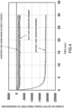
- the heat generated in the substrates 41 to 44 is released to the first casing portion 51 by the heat dissipation member 8, whereby the temperature drift of the infrared sensor 2 can be reduced as shown in FIG. 4 .
- the temperature drift of the infrared sensor 2 can also be reduced by bringing the first substrate 41 into direct contact with the first casing portion 51.
- FIG 4 is an experimental result showing a change in the output signal of the infrared sensor 2 in a case where the heat dissipation member 8 is not used and the place of the heat dissipation member 8 is a heat insulating layer, in a case where the heat dissipation member 8 is used, and in a case where the first substrate 41 is directly brought into contact with the first casing portion 51 and fixed with screws without using the heat dissipation member 8.
- the first casing portion 51 and the second casing portion 52 constituting the casing 5 are separated from each other.
- the first casing portion 51 and the second casing portion 52 may be formed of different members, and the first casing portion 51 and the second casing portion 52 may be formed of materials having different thermal conductivities.
- the front end surface of the first casing portion 51 and the rear end surface of the second casing portion 52 are connected so as to abut on each other.
- the connection is made using a screw (not illustrated).
- a third casing 53 from which the electric cable 6 extends is connected to a rear end surface of the first casing portion 51.
- first casing portion 51 and the second casing portion 52 are covered with a fourth casing portion 54, and here, a cylindrical gap S1 is formed between the fourth casing portion 54 and the first casing portion 51.
- the gap S1 functions as a heat insulating layer.
- the first casing portion 51 is provided with a diaphragm portion 9 that is provided in front of the incident side which is the measurement target side of the infrared sensor 2 and blocks heat radiation from the second casing portion 52.
- the diaphragm portion 9 forms a circular opening, and is formed on the front end side of the first casing portion 51.
- the diaphragm portion 9 can reduce thermal radiation from the second casing portion 52 incident on the infrared sensor 2.
- FIG. 5 is an experimental result showing a time change of the measured value (instruction value) in a case where the diaphragm portion 9 is not provided and a case where the diaphragm portion 9 is provided.
- a second wavelength selection filter 10 is provided in front of the incident side which is the measurement target side of the infrared sensor 2.
- the second wavelength selection filter 10 cuts transmission of wavelength bands other than the measurement wavelength that cannot be cut by the wavelength selection filter provided in the infrared sensor 2.
- the second wavelength selection filter 10 is provided on the front side of the diaphragm portion 9 in the first casing portion 51.
- the second wavelength selection filter 10 may not be provided.
- the second casing portion 52 includes a lens block 521 that holds the lens 3, and a casing main body 522 to which the lens block 521 is attached and detached, and the lens block 521 is configured to be replaceable with respect to the casing main body 522.
- the lens block 521 is prepared such that the length of the optical system and the type of the lens 3 are different according to the visual field characteristic, and is attached to the casing main body 522 according to the use of the radiation thermometer 100.
- the signal processing unit 4 since the signal processing unit 4 is configured by stacking the plurality of substrates 41 to 44 with the spacers 45 interposed therebetween, the signal processing unit 4 can be downsized and the circuit scale can be increased. As a result, the degree of freedom of the circuit accommodated in the casing 5 can be increased, and the analog signal from the infrared sensor 2 can be converted into the digital signal in the same casing 5 as the infrared sensor 2. Therefore, a digital signal can be output from the casing 5, and the configuration is resistant to electromagnetic noise.
- the signal processing unit 4 of the above embodiment is configured using the four substrates 41 to 44, but may be configured by stacking two or more substrates with a spacer interposed therebetween.
- the plurality of substrates may have different shapes.
- the spacers 45 are arranged in a row and the inter-substrate connectors 46 are arranged in a row in the stacking direction of the substrates 41 to 44.
- the spacers 45 and the inter-substrate connectors 46 may be alternately arranged in the stacking direction of the substrates 41 to 44.
- the first substrate 41 may be fixed in direct contact with the first casing portion 51 without using the heat dissipation member 8. Even in this case, as shown in FIG. 4 , it is possible to achieve an effect equivalent to or greater than that in the case of using the heat dissipation member 8.
- the elastic member 7 is configured to press the plurality of substrates 41 to 44 from the direction in which the plurality of substrates 41 to 44 are stacked, but may be configured to press the plurality of substrates 41 to 44 from the periphery.
- the heat dissipation member 8 is provided between the first casing portion 51 and the first substrate 41, but may be interposed between the third substrate 43 on which the temperature calculation unit (CPU) 4c is mounted and the first casing portion 51. Further, the heat dissipation member 8 may be interposed between each of the plurality of substrates 41 to 44 and the first casing portion 51.
- the functions of the signal processing unit 4 are divided into four and distributed to the four substrates 41 to 44, but the number of substrates to which the four functions are decomposed is not limited to four.
- the method of distributing the functions of the signal processing unit 4 to the plurality of substrates is not limited to the above embodiment.
- the casing 5 may be integrated without being separated into the first casing portion 51 and the second casing portion 52, or in the case where the casing 5 is separated into the first casing portion 51 and the second casing portion 52, a heat insulating member or a heat conduction member may be interposed therebetween.
- the lens block 521 is configured to be replaceable in the second casing portion 52, but the second casing portion 52 may be configured to be replaceable with respect to the first casing portion 51 so that the lens 3 can be replaced.
- the radiation thermometer can be downsized and the circuit scale can be increased.
Landscapes
- Physics & Mathematics (AREA)
- General Physics & Mathematics (AREA)
- Spectroscopy & Molecular Physics (AREA)
- Radiation Pyrometers (AREA)
- Photometry And Measurement Of Optical Pulse Characteristics (AREA)
Abstract
Description
- The present invention relates to a radiation thermometer.
- As disclosed in Patent Literature 1, the radiation thermometer is configured to detect infrared rays emitted from a measurement target with an infrared detection element (infrared sensor) so as to be able to measure the temperature of the measurement target based on the detected intensity.
- This radiation thermometer includes a measurement unit configured by accommodating an infrared sensor in a casing, and the measurement unit is desired to be downsized due to restrictions on an installation place and the like. Therefore, the casing of the measurement unit is usually configured to accommodate only the infrared sensor or to accommodate the infrared sensor and a preamplifier substrate. In addition, a calculation unit is connected to the measurement unit of the radiation thermometer via an electric cable, and the calculation unit is configured to calculate a temperature from an analog signal output from the measurement unit.
- However, as described above, when the measuring unit is downsized, only a minimum circuit can be accommodated in the casing. In addition, when the minimum circuit is accommodated in the casing, an analog signal from the infrared sensor is output to the outside, and the configuration is weak against electromagnetic noise (EMC noise).
- Patent Literature 1:
JP 2019-100987 A - Therefore, the present invention has been made to solve the above problems, and a main object of the present invention is to downsize a radiation thermometer and to increase a circuit scale.
- That is, a radiation thermometer according to the present invention includes: an infrared sensor; a signal processing unit that processes a signal of the infrared sensor; and a casing that accommodates the infrared sensor and the signal processing unit, in which the signal processing unit is configured by stacking a plurality of substrates with a spacer interposed therebetween.
- With such a configuration, since the signal processing unit is configured by stacking the plurality of substrates with the spacer interposed therebetween, the signal processing unit can be downsized and the circuit scale can be increased. As a result, the degree of freedom of the circuit accommodated in the casing can be increased, and an analog signal from the infrared sensor can be converted into a digital signal in the same casing as the infrared sensor. Therefore, a digital signal can be output from the casing, and the configuration is resistant to electromagnetic noise.
- Even in a case where the plurality of substrates are connected by an electric cable, the influence of electromagnetic noise is exerted. Therefore, it is desirable that the plurality of substrates be connected using an inter-substrate connector. Further, by connecting the plurality of substrates by the inter-substrate connector, connection between the substrates can be simplified.
- When a plurality of stacked substrates are fixed by screwing or the like, an excessive stress is applied to the substrates, and the plurality of substrates cannot be stably fixed. Therefore, it is desirable that the plurality of substrates be fixed to the casing with an elastic member interposed therebetween.
- When the plurality of substrates are connected by the inter-substrate connector, it is necessary to fix the inter-substrate connector so that the inter-substrate connector does not come off. Therefore, it is desirable that the elastic member press the plurality of substrates from a direction in which the plurality of substrates are stacked. With this configuration, the plurality of substrates can be stably fixed without coming off of the inter-substrate connector.
- In the present invention, it is conceivable that the infrared sensor is mounted on, for example, a first substrate located on an outermost side among the plurality of substrates. In the case of this configuration, the heat generated in the substrate is transmitted to the infrared sensor, and the output of the infrared sensor drifts. In order to suitably solve this problem, it is desirable that the first substrate be provided in contact with the casing or provided with a heat dissipation member interposed between the first substrate and the casing. With this configuration, the heat generated in the substrate can be released to the casing, so that the drift of the output of the infrared sensor can be reduced.
- In order to accurately measure the temperature of a measurement target, it is desirable that the radiation thermometer further include a lens provided in front of the infrared sensor.
- Here, in a case where the infrared sensor and the lens are accommodated in the same casing, it is necessary to take measures such as uniformizing the temperature distribution of the casing in order to cancel the thermal influence of the optical system such as the lens on the infrared sensor.
- Therefore, in the present invention, it is desirable that the casing include a first casing portion that accommodates the infrared sensor and the signal processing unit, and a second casing portion that accommodates the lens, and that the first casing portion and the second casing be configured to be separable from each other. With this configuration, since the first casing portion and the second casing portion are divided and thermally separated, the influence of the optical system such as the lens on the infrared sensor can be reduced.
- Here, when the infrared sensor detects thermal radiation from the second casing, a measurement error occurs. In order to reduce this measurement error, it is desirable that the first casing portion include a diaphragm portion that is provided in front of the infrared sensor and block heat radiation from the second casing portion. In addition, it is desirable that an inner diameter of the diaphragm portion be a diameter that blocks thermal radiation from the second casing portion without blocking infrared rays from a measurement target incident on the infrared sensor through the lens.
- In order to improve the measurement accuracy by the infrared sensor, it is conceivable to provide a wavelength selection filter in front of the infrared sensor. When the wavelength selection filter is provided in the second casing portion, the temperature difference between the infrared sensor and the wavelength selection filter increases, and the influence of the infrared light emitted from the wavelength selection filter is given. Therefore, it is desirable that the first casing portion include a wavelength selection filter provided in front of the infrared sensor. By providing the wavelength selection filter in the first casing portion in this manner, a temperature difference between the infrared sensor and the wavelength selection filter can be reduced, and a measurement error due to infrared rays emitted from the wavelength selection filter can be reduced.
- In order to be replaceable with various lenses according to the application of the radiation thermometer, it is desirable that the second casing portion include a lens block that holds the lens, and the lens block be configured to be replaceable.
- According to the present invention described above, the radiation thermometer can be downsized and the circuit scale can be increased.
-
-
FIG. 1 is a diagram schematically illustrating a configuration of a radiation thermometer according to an embodiment of the present invention. -
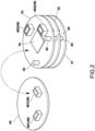
FIG. 2 is a perspective view illustrating a state in which a fourth substrate is separated from a third substrate in the embodiment. -
FIG. 3 is a schematic diagram illustrating a flow of heat of the embodiment. -
FIG. 4 is an experimental result showing the presence or absence of a heat dissipation member and a time change in an output signal of an infrared sensor in a case where a substrate and a casing are in direct contact with each other. -
FIG. 5 is an experimental result showing a time change of a measured value (instruction value) depending on the presence or absence of a diaphragm portion. -
FIG. 6 is an experimental result showing a time change of a measured value (instruction value) in a case where a wavelength selection filter is provided in a lens unit and in a case where the wavelength selection filter is provided in a sensor unit. -
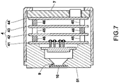
FIG. 7 is a cross-sectional view illustrating configurations of spacers and inter-substrate connectors in a signal processing unit of a modified embodiment. -
- 100
- radiation thermometer
- 2
- infrared sensor
- 3
- lens
- 4
- signal processing unit
- 41
- first substrate
- 42
- second substrate
- 43
- third substrate
- 44
- fourth substrate
- 45
- spacer
- 46
- inter-substrate connector
- 5
- casing
- 51
- first casing portion
- 52
- second casing portion
- 521
- lens block
- 7
- elastic member
- 8
- heat dissipation member
- 9
- diaphragm portion
- 10
- wavelength selection filter
- Hereinafter, a radiation thermometer according to an embodiment of the present invention will be described with reference to the drawings.
- A
radiation thermometer 100 according to the present embodiment measures a temperature of a measurement target in a non-contact manner based on the intensity of infrared rays emitted from the measurement target. - Specifically, the
radiation thermometer 100 includes aninfrared sensor 2, alens 3 provided in front of an incident side that is a measurement target side of theinfrared sensor 2, asignal processing unit 4 that processes a signal of theinfrared sensor 2 to calculate a temperature, and acasing 5 that accommodates theinfrared sensor 2 and thesignal processing unit 4. Note that the temperature data calculated by thesignal processing unit 4 is output to an external device (not illustrated) such as anexternal display unit 200 or a temperature control device via anelectric cable 6. - The
infrared sensor 2 detects infrared rays emitted from a measurement target and outputs an intensity signal (analog signal) corresponding to energy of the detected infrared rays. Specifically, theinfrared sensor 2 detects infrared rays in the entire wavelength band of the infrared wavelength band, for example, and is a thermal-type sensor such as a thermopile here. As the infrared sensor, other types, for example, quantum photoelectric elements such as HgCdTe, InGaAs, InAsSb, and PbSe may be used. Furthermore, theinfrared sensor 2 is provided with a wavelength selection filter (not illustrated) that passes only light (electromagnetic wave) in a predetermined wavelength band. Here, for example, one that passes only infrared rays in a band with a wavelength of 8 µm to 14 µm is used, and only infrared rays that have passed through thewavelength selection filter 10 are received. - The
lens 3 is an infrared lens that condenses infrared rays emitted from a measurement target on theinfrared sensor 2. In the present embodiment, a plano-convex lens in which one surface is a convex surface and the other surface is a flat surface is used. In addition, thelens 3 has a circular shape in plan view. Note that thelens 3 may be a biconvex lens having convex surfaces on both sides, or the shape and size may be appropriately changed. - The
signal processing unit 4 processes the analog signal of theinfrared sensor 2 and calculates the temperature of the measurement target. Thesignal processing unit 4 includes anamplification unit 4a that amplifies an analog signal of theinfrared sensor 2, anAD conversion unit 4b that converts the amplified analog signal into a digital signal, atemperature calculation unit 4c such as a CPU that calculates a temperature from the AD-converted digital signal, and an input/output interface unit 4d that outputs temperature data (digital signal) indicating the calculated temperature to the outside. - The
casing 5 accommodates theinfrared sensor 2, thesignal processing unit 4, and thelens 3, and has a substantially cylindrical shape. Thecasing 5 includes afirst casing portion 51 that accommodates theinfrared sensor 2 and thesignal processing unit 4, and asecond casing portion 52 that accommodates thelens 3. Thefirst casing portion 51 and thesecond casing portion 52 are desirably made of a material having high thermal conductivity, such as aluminum or copper. - Thus, as illustrated in
FIG. 1 , thesignal processing unit 4 of the present embodiment is configured by stacking a plurality ofsubstrates 41 to 44 in the thickness direction withspacers 45 interposed therebetween. In the present embodiment, a four-stage configuration in which foursubstrates 41 to 44 are stacked with thespacers 45 interposed therebetween is employed. - The
infrared sensor 2 is soldered and mounted on the upper surface of thefirst substrate 41 located at the uppermost stage (foremost side inFIG. 1 ) which is the outermost side. In addition, thefirst substrate 41 is provided with anamplification unit 4a that amplifies an analog signal of theinfrared sensor 2. Here, since theinfrared sensor 2 is mounted on the upper surface of thefirst substrate 41, theamplification unit 4a is provided on the back surface of thefirst substrate 41. - On the
second substrate 42 next to thefirst substrate 41, anAD conversion unit 4b that converts the analog signal amplified by theamplification unit 4a into a digital signal is mounted. InFIG. 1 , theAD conversion unit 4b is mounted on the back surface of thesecond substrate 42 so as not to physically interfere with theamplification unit 4a, but may be provided on the upper surface of thesecond substrate 42. - Furthermore, the
third substrate 43 next to thesecond substrate 42 is provided with atemperature calculation unit 4c such as a CPU that calculates a temperature from the converted digital signal. InFIG. 1 , thetemperature calculation unit 4c is mounted on the back surface of thethird substrate 43 so as not to physically interfere with theAD conversion unit 4b, but may be provided on the upper surface of thethird substrate 43. - Further, thereon, the
fourth substrate 44 next to thethird substrate 43 is provided with an input/output interface unit 4d for outputting the temperature data calculated by thetemperature calculation unit 4c to the outside. Theelectric cable 6 connected to an external device via a connector is connected to thefourth substrate 44. - These
substrates 41 to 44 are separated by a predetermined distance by thespacer 45. The spacer may be, for example, copper plated with tin or aluminum plated with tin. One or a plurality ofspacers 45 are provided between the substrates adjacent to each other. Thespacers 45 prevent theelectronic components 4a to 4d mounted on therespective substrates 41 to 44 from physically interfering with another substrate or an electronic component mounted on another substrate. - Further, these
substrates 41 to 44 are connected usinginter-substrate connectors 46. Theinter-substrate connector 46 is of a fitting type and is vertically connected. Specifically, as illustrated inFIG. 2 , theinter-substrate connector 46 includes aplug 461 provided on one of opposing surfaces of two boards adjacent to each other, and areceptacle 462 provided on the other. Note that theinter-substrate connector 46 also has a function similar to that of thespacer 45 described above, and causes thesubstrates 41 to 44 to be separated from each other by a predetermined distance. - The plurality of
substrates 41 to 44 constituting thesignal processing unit 4 are fixed to the casing 5 (here, the first casing portion 51) via anelastic member 7 such as silicone rubber. Specifically, theelastic member 7 is interposed between thefirst casing portion 51 and the plurality ofsubstrates 41 to 44 to press the plurality ofsubstrates 41 to 44 from a direction in which the plurality ofsubstrates 41 to 44 are stacked (front-rear direction inFIG. 1 ). In the present embodiment, theelastic member 7 is provided between thefourth substrate 44 opposite to thefirst substrate 41 on which theinfrared sensor 2 is mounted and thefirst casing portion 51. - Here, a
heat dissipation member 8 is provided between thefirst substrate 41 and thefirst casing portion 51. That is, theheat dissipation member 8 is provided in contact with thefirst substrate 41, and theheat dissipation member 8 is provided in contact with thefirst casing portion 51. Note that, in relation to theelastic member 7 described above, the plurality ofsubstrates 41 to 44 have a structure sandwiched between theelastic member 7 and theheat dissipation member 8. Thefirst substrate 41 may be brought into direct contact with thefirst casing portion 51 without providing theheat dissipation member 8. - The
heat dissipation member 8 is, for example, an acrylic or silicone-based sheet. Theheat dissipation member 8 releases the heat generated in thesubstrates 41 to 44 to thefirst casing portion 51, thereby reducing the temperature drift of theinfrared sensor 2. Theheat dissipation member 8 is provided so as to surround theinfrared sensor 2 on thefirst substrate 41. Among the electronic components mounted on the plurality ofsubstrates 41 to 44, the heat generation of the temperature calculation unit (CPU) 4c is large, and as illustrated inFIG. 3 , the heat from thethird substrate 43 on which thetemperature calculation unit 4c is mounted is transferred mainly to thefirst substrate 41 side with thespacers 45 interposed therebetween. The heat transferred to thefirst substrate 41 is transferred to thefirst casing portion 51 via theheat dissipation member 8. As described above, the heat generated in thesubstrates 41 to 44 is released to thefirst casing portion 51 by theheat dissipation member 8, whereby the temperature drift of theinfrared sensor 2 can be reduced as shown inFIG. 4 . The temperature drift of theinfrared sensor 2 can also be reduced by bringing thefirst substrate 41 into direct contact with thefirst casing portion 51.FIG. 4 is an experimental result showing a change in the output signal of theinfrared sensor 2 in a case where theheat dissipation member 8 is not used and the place of theheat dissipation member 8 is a heat insulating layer, in a case where theheat dissipation member 8 is used, and in a case where thefirst substrate 41 is directly brought into contact with thefirst casing portion 51 and fixed with screws without using theheat dissipation member 8. - The
first casing portion 51 and thesecond casing portion 52 constituting thecasing 5 are separated from each other. Specifically, thefirst casing portion 51 and thesecond casing portion 52 may be formed of different members, and thefirst casing portion 51 and thesecond casing portion 52 may be formed of materials having different thermal conductivities. In addition, the front end surface of thefirst casing portion 51 and the rear end surface of thesecond casing portion 52 are connected so as to abut on each other. Here, the connection is made using a screw (not illustrated). Athird casing 53 from which theelectric cable 6 extends is connected to a rear end surface of thefirst casing portion 51. In addition, the outer peripheral surfaces of thefirst casing portion 51 and thesecond casing portion 52 are covered with afourth casing portion 54, and here, a cylindrical gap S1 is formed between thefourth casing portion 54 and thefirst casing portion 51. The gap S1 functions as a heat insulating layer. - The
first casing portion 51 is provided with adiaphragm portion 9 that is provided in front of the incident side which is the measurement target side of theinfrared sensor 2 and blocks heat radiation from thesecond casing portion 52. Thediaphragm portion 9 forms a circular opening, and is formed on the front end side of thefirst casing portion 51. Thediaphragm portion 9 can reduce thermal radiation from thesecond casing portion 52 incident on theinfrared sensor 2. As a result, as shown inFIG. 5 , it is possible to prevent deterioration of the measured value (instruction value) due to temperature influence caused by separation of a sensor unit (thefirst casing portion 51 accommodating the infrared sensor 2) and a lens unit (thesecond casing portion 52 accommodating the lens 3).FIG. 5 is an experimental result showing a time change of the measured value (instruction value) in a case where thediaphragm portion 9 is not provided and a case where thediaphragm portion 9 is provided. - In the
first casing portion 51, a secondwavelength selection filter 10 is provided in front of the incident side which is the measurement target side of theinfrared sensor 2. The secondwavelength selection filter 10 cuts transmission of wavelength bands other than the measurement wavelength that cannot be cut by the wavelength selection filter provided in theinfrared sensor 2. Specifically, the secondwavelength selection filter 10 is provided on the front side of thediaphragm portion 9 in thefirst casing portion 51. By providing thesecond filter 10 in thefirst casing portion 51 in this manner, as shown inFIG. 6 , as compared with the case where the second filter is provided in the second casing portion 52 (lens unit), it is possible to reduce the temperature difference between theinfrared sensor 2 and the secondwavelength selection filter 10 and to prevent deterioration of the measured value (instruction value) due to the temperature influence. Note that the secondwavelength selection filter 10 may not be provided. - On the other hand, the
second casing portion 52 includes alens block 521 that holds thelens 3, and a casingmain body 522 to which thelens block 521 is attached and detached, and thelens block 521 is configured to be replaceable with respect to the casingmain body 522. Thelens block 521 is prepared such that the length of the optical system and the type of thelens 3 are different according to the visual field characteristic, and is attached to the casingmain body 522 according to the use of theradiation thermometer 100. - According to the
radiation thermometer 100 of the present embodiment, since thesignal processing unit 4 is configured by stacking the plurality ofsubstrates 41 to 44 with thespacers 45 interposed therebetween, thesignal processing unit 4 can be downsized and the circuit scale can be increased. As a result, the degree of freedom of the circuit accommodated in thecasing 5 can be increased, and the analog signal from theinfrared sensor 2 can be converted into the digital signal in thesame casing 5 as theinfrared sensor 2. Therefore, a digital signal can be output from thecasing 5, and the configuration is resistant to electromagnetic noise. - Note that the present invention is not limited to the above embodiment.
- For example, the
signal processing unit 4 of the above embodiment is configured using the foursubstrates 41 to 44, but may be configured by stacking two or more substrates with a spacer interposed therebetween. The plurality of substrates may have different shapes. - In the above embodiment, in the
substrates 41 to 44, thespacers 45 are arranged in a row and theinter-substrate connectors 46 are arranged in a row in the stacking direction of thesubstrates 41 to 44. However, as illustrated inFIG. 7 , in thesubstrates 41 to 44, thespacers 45 and theinter-substrate connectors 46 may be alternately arranged in the stacking direction of thesubstrates 41 to 44. As illustrated inFIG. 7 , thefirst substrate 41 may be fixed in direct contact with thefirst casing portion 51 without using theheat dissipation member 8. Even in this case, as shown inFIG. 4 , it is possible to achieve an effect equivalent to or greater than that in the case of using theheat dissipation member 8. - In the above embodiment, the
elastic member 7 is configured to press the plurality ofsubstrates 41 to 44 from the direction in which the plurality ofsubstrates 41 to 44 are stacked, but may be configured to press the plurality ofsubstrates 41 to 44 from the periphery. - In the above embodiment, the
heat dissipation member 8 is provided between thefirst casing portion 51 and thefirst substrate 41, but may be interposed between thethird substrate 43 on which the temperature calculation unit (CPU) 4c is mounted and thefirst casing portion 51. Further, theheat dissipation member 8 may be interposed between each of the plurality ofsubstrates 41 to 44 and thefirst casing portion 51. - In the above embodiment, the functions of the
signal processing unit 4 are divided into four and distributed to the foursubstrates 41 to 44, but the number of substrates to which the four functions are decomposed is not limited to four. The method of distributing the functions of thesignal processing unit 4 to the plurality of substrates is not limited to the above embodiment. - Furthermore, the
casing 5 may be integrated without being separated into thefirst casing portion 51 and thesecond casing portion 52, or in the case where thecasing 5 is separated into thefirst casing portion 51 and thesecond casing portion 52, a heat insulating member or a heat conduction member may be interposed therebetween. - Moreover, in the above embodiment, the
lens block 521 is configured to be replaceable in thesecond casing portion 52, but thesecond casing portion 52 may be configured to be replaceable with respect to thefirst casing portion 51 so that thelens 3 can be replaced. - In addition, various modifications and combinations of the embodiments may be made without departing from the gist of the present invention.
- According to the present invention, the radiation thermometer can be downsized and the circuit scale can be increased.
Claims (9)
- A radiation thermometer comprising:an infrared sensor;a signal processing unit that processes a signal of the infrared sensor; anda casing that accommodates the infrared sensor and the signal processing unit,wherein the signal processing unit is configured by stacking a plurality of substrates with a spacer interposed therebetween.
- The radiation thermometer according to claim 1, wherein the plurality of substrates are connected using an inter-substrate connector.
- The radiation thermometer according to claim 1 or 2, wherein the plurality of substrates are fixed to the casing with an elastic member interposed therebetween.
- The radiation thermometer according to claim 3, wherein the elastic member presses the plurality of substrates from a direction in which the plurality of substrates are stacked.
- The radiation thermometer according to any one of claims 1 to 4, whereinthe plurality of substrates include a first substrate on which the infrared sensor is mounted, andthe first substrate is provided in contact with the casing or provided with a heat dissipation member interposed between the first substrate and the casing.
- The radiation thermometer according to any one of claims 1 to 5, further comprising a lens provided in front of the infrared sensor,wherein the casing includes a first casing portion that accommodates the infrared sensor and the signal processing unit, and a second casing portion that accommodates the lens, andthe first casing portion and the second casing are configured to be separable from each other.
- The radiation thermometer according to claim 6, wherein the first casing portion includes a diaphragm portion that is provided in front of the infrared sensor and blocks heat radiation from the second casing portion.
- The radiation thermometer according to claim 6 or 7, wherein the first casing portion includes a wavelength selection filter provided in front of the infrared sensor.
- The radiation thermometer according to any one of claims 6 to 8, wherein the second casing portion includes a lens block that holds the lens, and the lens block is configured to be replaceable.
Applications Claiming Priority (2)
| Application Number | Priority Date | Filing Date | Title |
|---|---|---|---|
| JP2020111469 | 2020-06-29 | ||
| PCT/JP2021/023721 WO2022004507A1 (en) | 2020-06-29 | 2021-06-23 | Radiation thermometer |
Publications (3)
| Publication Number | Publication Date |
|---|---|
| EP4141395A1 true EP4141395A1 (en) | 2023-03-01 |
| EP4141395A4 EP4141395A4 (en) | 2024-04-24 |
| EP4141395B1 EP4141395B1 (en) | 2025-08-27 |
Family
ID=79316209
Family Applications (1)
| Application Number | Title | Priority Date | Filing Date |
|---|---|---|---|
| EP21832673.4A Active EP4141395B1 (en) | 2020-06-29 | 2021-06-23 | Radiation thermometer |
Country Status (5)
| Country | Link |
|---|---|
| US (1) | US12416527B2 (en) |
| EP (1) | EP4141395B1 (en) |
| JP (1) | JP7591572B2 (en) |
| CN (1) | CN115667863A (en) |
| WO (1) | WO2022004507A1 (en) |
Families Citing this family (4)
| Publication number | Priority date | Publication date | Assignee | Title |
|---|---|---|---|---|
| CN114641671A (en) * | 2019-11-18 | 2022-06-17 | 株式会社村田制作所 | Optical sensor |
| CN114641672A (en) * | 2019-11-18 | 2022-06-17 | 株式会社村田制作所 | Optical sensor |
| WO2026053726A1 (en) * | 2024-09-04 | 2026-03-12 | コニカミノルタ株式会社 | Photometric/colorimetric device |
| WO2026053720A1 (en) * | 2024-09-04 | 2026-03-12 | コニカミノルタ株式会社 | Photometric/colorimetric device |
Family Cites Families (22)
| Publication number | Priority date | Publication date | Assignee | Title |
|---|---|---|---|---|
| JPH0531536Y2 (en) * | 1986-05-09 | 1993-08-13 | ||
| US5512748A (en) * | 1994-07-26 | 1996-04-30 | Texas Instruments Incorporated | Thermal imaging system with a monolithic focal plane array and method |
| DE19535408A1 (en) * | 1995-09-23 | 1997-03-27 | Braun Ag | Infrared radiation thermometer for medical use |
| DE19600334C2 (en) * | 1996-01-08 | 2002-11-14 | Braun Gmbh | Process for evaluating the measurement signal supplied by an infrared sensor of an infrared thermometer, and infrared thermometer |
| DE19713608A1 (en) * | 1997-04-02 | 1998-10-08 | Braun Ag | Measuring tip for radiation thermometer |
| DE19842403B4 (en) * | 1998-09-16 | 2004-05-06 | Braun Gmbh | Radiation sensor with several sensor elements |
| JP2003188489A (en) | 2001-12-14 | 2003-07-04 | Pentax Corp | Electronic scope board structure |
| JP4555148B2 (en) * | 2005-01-07 | 2010-09-29 | 株式会社キーエンス | Radiation thermometer |
| JP2006226864A (en) * | 2005-02-18 | 2006-08-31 | Keyence Corp | Radiation thermometer |
| US7718970B2 (en) * | 2005-11-25 | 2010-05-18 | Panasonic Electric Works Co., Ltd. | Infrared detection unit using a semiconductor optical lens |
| JP5451957B2 (en) * | 2006-02-23 | 2014-03-26 | パナソニック株式会社 | Infrared detector |
| US7402802B1 (en) * | 2006-10-19 | 2008-07-22 | Flir Systems, Inc. | Infrared camera packaging systems and methods |
| JP2008187284A (en) | 2007-01-26 | 2008-08-14 | Fujitsu General Ltd | Camera device |
| JP2009002739A (en) | 2007-06-20 | 2009-01-08 | Horiba Ltd | Radiation thermometer |
| EP2511679A1 (en) | 2009-12-09 | 2012-10-17 | Panasonic Corporation | Infrared flame detector |
| KR102255446B1 (en) | 2014-08-04 | 2021-05-24 | 엘지이노텍 주식회사 | Camera module for vehicle |
| EP3078951A1 (en) * | 2015-04-10 | 2016-10-12 | Silverlight AG | Device with a pir sensor |
| JP5866585B1 (en) * | 2015-05-20 | 2016-02-17 | パナソニックIpマネジメント株式会社 | Light receiving sensor, air conditioner and electronic cooker using the same |
| JPWO2018008215A1 (en) * | 2016-07-04 | 2019-04-18 | 株式会社堀場製作所 | Infrared detector and radiation thermometer |
| JP6720033B2 (en) * | 2016-09-14 | 2020-07-08 | 株式会社Screenホールディングス | Heat treatment equipment |
| JP7137925B2 (en) | 2017-12-08 | 2022-09-15 | 株式会社 堀場アドバンスドテクノ | radiation thermometer |
| CN109405978A (en) | 2018-11-28 | 2019-03-01 | 西安泰豪红外科技有限公司 | A kind of infrared machine core of refrigeration mode and preparation method thereof |
-
2021
- 2021-06-23 US US17/999,015 patent/US12416527B2/en active Active
- 2021-06-23 EP EP21832673.4A patent/EP4141395B1/en active Active
- 2021-06-23 JP JP2022533903A patent/JP7591572B2/en active Active
- 2021-06-23 WO PCT/JP2021/023721 patent/WO2022004507A1/en not_active Ceased
- 2021-06-23 CN CN202180035920.5A patent/CN115667863A/en active Pending
Also Published As
| Publication number | Publication date |
|---|---|
| EP4141395B1 (en) | 2025-08-27 |
| CN115667863A (en) | 2023-01-31 |
| JP7591572B2 (en) | 2024-11-28 |
| US20230194350A1 (en) | 2023-06-22 |
| EP4141395A4 (en) | 2024-04-24 |
| US12416527B2 (en) | 2025-09-16 |
| WO2022004507A1 (en) | 2022-01-06 |
| JPWO2022004507A1 (en) | 2022-01-06 |
Similar Documents
| Publication | Publication Date | Title |
|---|---|---|
| EP4141395B1 (en) | Radiation thermometer | |
| US20210372854A1 (en) | Optical detection device having adhesive member | |
| US8952331B2 (en) | Infrared sensor module | |
| US20220333988A1 (en) | Light detection device | |
| EP4467942A2 (en) | Light detection device | |
| KR102641685B1 (en) | Spectrometer, and method of manufacturing the spectrometer | |
| EP2267423B1 (en) | Protective enclosure for a thermal imaging device of an industrial monitoring system | |
| JPWO2009081748A1 (en) | Radiation temperature measurement method and radiation temperature measurement system | |
| JP6350933B2 (en) | Infrared detector | |
| US20110304754A1 (en) | Image sensor module and camera module | |
| US4242581A (en) | Laser energy monitor | |
| JP5564681B2 (en) | Infrared sensor | |
| JP7137925B2 (en) | radiation thermometer | |
| JP6682408B2 (en) | Temperature control module | |
| ATE529895T1 (en) | DEVICE HAVING A SHIELDED SANDWICH STRUCTURE FOR DETECTING HEAT RADIATION AND USE OF THE DEVICE | |
| EP4177962B1 (en) | Infrared sensor and infrared sensor manufacturing method | |
| JP2010175442A (en) | Thermopile type infrared detector | |
| CN222213186U (en) | Laser module and laser projection device | |
| US20220412801A1 (en) | Spectral module and method for manufacturing spectral module | |
| JP2023179039A (en) | infrared sensor | |
| KR20180061994A (en) | Multi gas sensing package | |
| CN104776916A (en) | Infrared sensor | |
| JP6476873B2 (en) | Photodetection device, photodetection module, and electronic device | |
| JP2011123024A (en) | Photosensor | |
| CN112629672A (en) | Sensor and temperature measuring device |
Legal Events
| Date | Code | Title | Description |
|---|---|---|---|
| STAA | Information on the status of an ep patent application or granted ep patent |
Free format text: STATUS: THE INTERNATIONAL PUBLICATION HAS BEEN MADE |
|
| PUAI | Public reference made under article 153(3) epc to a published international application that has entered the european phase |
Free format text: ORIGINAL CODE: 0009012 |
|
| STAA | Information on the status of an ep patent application or granted ep patent |
Free format text: STATUS: REQUEST FOR EXAMINATION WAS MADE |
|
| 17P | Request for examination filed |
Effective date: 20221123 |
|
| AK | Designated contracting states |
Kind code of ref document: A1 Designated state(s): AL AT BE BG CH CY CZ DE DK EE ES FI FR GB GR HR HU IE IS IT LI LT LU LV MC MK MT NL NO PL PT RO RS SE SI SK SM TR |
|
| DAV | Request for validation of the european patent (deleted) | ||
| DAX | Request for extension of the european patent (deleted) | ||
| P01 | Opt-out of the competence of the unified patent court (upc) registered |
Effective date: 20231108 |
|
| A4 | Supplementary search report drawn up and despatched |
Effective date: 20240322 |
|
| RIC1 | Information provided on ipc code assigned before grant |
Ipc: G01J 5/06 20220101ALI20240319BHEP Ipc: G01J 5/0806 20220101ALI20240319BHEP Ipc: G01J 5/04 20060101ALI20240319BHEP Ipc: G01J 5/02 20220101AFI20240319BHEP |
|
| GRAP | Despatch of communication of intention to grant a patent |
Free format text: ORIGINAL CODE: EPIDOSNIGR1 |
|
| STAA | Information on the status of an ep patent application or granted ep patent |
Free format text: STATUS: GRANT OF PATENT IS INTENDED |
|
| RIC1 | Information provided on ipc code assigned before grant |
Ipc: G01J 5/06 20220101ALI20250423BHEP Ipc: G01J 5/0806 20220101ALI20250423BHEP Ipc: G01J 5/04 20060101ALI20250423BHEP Ipc: G01J 5/02 20220101AFI20250423BHEP |
|
| INTG | Intention to grant announced |
Effective date: 20250509 |
|
| GRAS | Grant fee paid |
Free format text: ORIGINAL CODE: EPIDOSNIGR3 |
|
| GRAA | (expected) grant |
Free format text: ORIGINAL CODE: 0009210 |
|
| STAA | Information on the status of an ep patent application or granted ep patent |
Free format text: STATUS: THE PATENT HAS BEEN GRANTED |
|
| AK | Designated contracting states |
Kind code of ref document: B1 Designated state(s): AL AT BE BG CH CY CZ DE DK EE ES FI FR GB GR HR HU IE IS IT LI LT LU LV MC MK MT NL NO PL PT RO RS SE SI SK SM TR |
|
| REG | Reference to a national code |
Ref country code: CH Ref legal event code: EP |
|
| REG | Reference to a national code |
Ref country code: DE Ref legal event code: R096 Ref document number: 602021037361 Country of ref document: DE |
|
| REG | Reference to a national code |
Ref country code: IE Ref legal event code: FG4D |
|
| REG | Reference to a national code |
Ref country code: NL Ref legal event code: MP Effective date: 20250827 |
|
| PG25 | Lapsed in a contracting state [announced via postgrant information from national office to epo] |
Ref country code: IS Free format text: LAPSE BECAUSE OF FAILURE TO SUBMIT A TRANSLATION OF THE DESCRIPTION OR TO PAY THE FEE WITHIN THE PRESCRIBED TIME-LIMIT Effective date: 20251227 |
|
| PG25 | Lapsed in a contracting state [announced via postgrant information from national office to epo] |
Ref country code: NO Free format text: LAPSE BECAUSE OF FAILURE TO SUBMIT A TRANSLATION OF THE DESCRIPTION OR TO PAY THE FEE WITHIN THE PRESCRIBED TIME-LIMIT Effective date: 20251127 |
|
| REG | Reference to a national code |
Ref country code: LT Ref legal event code: MG9D |
|
| PG25 | Lapsed in a contracting state [announced via postgrant information from national office to epo] |
Ref country code: PT Free format text: LAPSE BECAUSE OF FAILURE TO SUBMIT A TRANSLATION OF THE DESCRIPTION OR TO PAY THE FEE WITHIN THE PRESCRIBED TIME-LIMIT Effective date: 20251229 |
|
| PG25 | Lapsed in a contracting state [announced via postgrant information from national office to epo] |
Ref country code: FI Free format text: LAPSE BECAUSE OF FAILURE TO SUBMIT A TRANSLATION OF THE DESCRIPTION OR TO PAY THE FEE WITHIN THE PRESCRIBED TIME-LIMIT Effective date: 20250827 |
|
| PG25 | Lapsed in a contracting state [announced via postgrant information from national office to epo] |
Ref country code: NL Free format text: LAPSE BECAUSE OF FAILURE TO SUBMIT A TRANSLATION OF THE DESCRIPTION OR TO PAY THE FEE WITHIN THE PRESCRIBED TIME-LIMIT Effective date: 20250827 Ref country code: HR Free format text: LAPSE BECAUSE OF FAILURE TO SUBMIT A TRANSLATION OF THE DESCRIPTION OR TO PAY THE FEE WITHIN THE PRESCRIBED TIME-LIMIT Effective date: 20250827 |
|
| PG25 | Lapsed in a contracting state [announced via postgrant information from national office to epo] |
Ref country code: GR Free format text: LAPSE BECAUSE OF FAILURE TO SUBMIT A TRANSLATION OF THE DESCRIPTION OR TO PAY THE FEE WITHIN THE PRESCRIBED TIME-LIMIT Effective date: 20251128 |
|
| PG25 | Lapsed in a contracting state [announced via postgrant information from national office to epo] |
Ref country code: SE Free format text: LAPSE BECAUSE OF FAILURE TO SUBMIT A TRANSLATION OF THE DESCRIPTION OR TO PAY THE FEE WITHIN THE PRESCRIBED TIME-LIMIT Effective date: 20250827 |
|
| PG25 | Lapsed in a contracting state [announced via postgrant information from national office to epo] |
Ref country code: LV Free format text: LAPSE BECAUSE OF FAILURE TO SUBMIT A TRANSLATION OF THE DESCRIPTION OR TO PAY THE FEE WITHIN THE PRESCRIBED TIME-LIMIT Effective date: 20250827 |
|
| PG25 | Lapsed in a contracting state [announced via postgrant information from national office to epo] |
Ref country code: PL Free format text: LAPSE BECAUSE OF FAILURE TO SUBMIT A TRANSLATION OF THE DESCRIPTION OR TO PAY THE FEE WITHIN THE PRESCRIBED TIME-LIMIT Effective date: 20250827 Ref country code: BG Free format text: LAPSE BECAUSE OF FAILURE TO SUBMIT A TRANSLATION OF THE DESCRIPTION OR TO PAY THE FEE WITHIN THE PRESCRIBED TIME-LIMIT Effective date: 20250827 |
|
| PG25 | Lapsed in a contracting state [announced via postgrant information from national office to epo] |
Ref country code: RS Free format text: LAPSE BECAUSE OF FAILURE TO SUBMIT A TRANSLATION OF THE DESCRIPTION OR TO PAY THE FEE WITHIN THE PRESCRIBED TIME-LIMIT Effective date: 20251127 |
|
| PG25 | Lapsed in a contracting state [announced via postgrant information from national office to epo] |
Ref country code: ES Free format text: LAPSE BECAUSE OF FAILURE TO SUBMIT A TRANSLATION OF THE DESCRIPTION OR TO PAY THE FEE WITHIN THE PRESCRIBED TIME-LIMIT Effective date: 20250827 |
|
| PG25 | Lapsed in a contracting state [announced via postgrant information from national office to epo] |
Ref country code: SM Free format text: LAPSE BECAUSE OF FAILURE TO SUBMIT A TRANSLATION OF THE DESCRIPTION OR TO PAY THE FEE WITHIN THE PRESCRIBED TIME-LIMIT Effective date: 20250827 |
|
| PG25 | Lapsed in a contracting state [announced via postgrant information from national office to epo] |
Ref country code: DK Free format text: LAPSE BECAUSE OF FAILURE TO SUBMIT A TRANSLATION OF THE DESCRIPTION OR TO PAY THE FEE WITHIN THE PRESCRIBED TIME-LIMIT Effective date: 20250827 |
|
| PG25 | Lapsed in a contracting state [announced via postgrant information from national office to epo] |
Ref country code: IT Free format text: LAPSE BECAUSE OF FAILURE TO SUBMIT A TRANSLATION OF THE DESCRIPTION OR TO PAY THE FEE WITHIN THE PRESCRIBED TIME-LIMIT Effective date: 20250827 |
|
| PG25 | Lapsed in a contracting state [announced via postgrant information from national office to epo] |
Ref country code: CZ Free format text: LAPSE BECAUSE OF FAILURE TO SUBMIT A TRANSLATION OF THE DESCRIPTION OR TO PAY THE FEE WITHIN THE PRESCRIBED TIME-LIMIT Effective date: 20250827 |
|
| PG25 | Lapsed in a contracting state [announced via postgrant information from national office to epo] |
Ref country code: EE Free format text: LAPSE BECAUSE OF FAILURE TO SUBMIT A TRANSLATION OF THE DESCRIPTION OR TO PAY THE FEE WITHIN THE PRESCRIBED TIME-LIMIT Effective date: 20250827 Ref country code: SK Free format text: LAPSE BECAUSE OF FAILURE TO SUBMIT A TRANSLATION OF THE DESCRIPTION OR TO PAY THE FEE WITHIN THE PRESCRIBED TIME-LIMIT Effective date: 20250827 |