EP4138121A1 - Diode laser for wafer heating for epi processes - Google Patents
Diode laser for wafer heating for epi processes Download PDFInfo
- Publication number
- EP4138121A1 EP4138121A1 EP22198121.0A EP22198121A EP4138121A1 EP 4138121 A1 EP4138121 A1 EP 4138121A1 EP 22198121 A EP22198121 A EP 22198121A EP 4138121 A1 EP4138121 A1 EP 4138121A1
- Authority
- EP
- European Patent Office
- Prior art keywords
- substrate
- process chamber
- disposed
- source assembly
- susceptor
- Prior art date
- Legal status (The legal status is an assumption and is not a legal conclusion. Google has not performed a legal analysis and makes no representation as to the accuracy of the status listed.)
- Pending
Links
Images




Classifications
-
- H—ELECTRICITY
- H01—ELECTRIC ELEMENTS
- H01J—ELECTRIC DISCHARGE TUBES OR DISCHARGE LAMPS
- H01J37/00—Discharge tubes with provision for introducing objects or material to be exposed to the discharge, e.g. for the purpose of examination or processing thereof
- H01J37/32—Gas-filled discharge tubes
- H01J37/32431—Constructional details of the reactor
- H01J37/32715—Workpiece holder
- H01J37/32724—Temperature
-
- H—ELECTRICITY
- H10—SEMICONDUCTOR DEVICES; ELECTRIC SOLID-STATE DEVICES NOT OTHERWISE PROVIDED FOR
- H10P—GENERIC PROCESSES OR APPARATUS FOR THE MANUFACTURE OR TREATMENT OF DEVICES COVERED BY CLASS H10
- H10P72/00—Handling or holding of wafers, substrates or devices during manufacture or treatment thereof
- H10P72/04—Apparatus for manufacture or treatment
- H10P72/0431—Apparatus for thermal treatment
- H10P72/0436—Apparatus for thermal treatment mainly by radiation
-
- H—ELECTRICITY
- H01—ELECTRIC ELEMENTS
- H01J—ELECTRIC DISCHARGE TUBES OR DISCHARGE LAMPS
- H01J37/00—Discharge tubes with provision for introducing objects or material to be exposed to the discharge, e.g. for the purpose of examination or processing thereof
- H01J37/32—Gas-filled discharge tubes
- H01J37/32431—Constructional details of the reactor
- H01J37/3244—Gas supply means
-
- H—ELECTRICITY
- H10—SEMICONDUCTOR DEVICES; ELECTRIC SOLID-STATE DEVICES NOT OTHERWISE PROVIDED FOR
- H10P—GENERIC PROCESSES OR APPARATUS FOR THE MANUFACTURE OR TREATMENT OF DEVICES COVERED BY CLASS H10
- H10P34/00—Irradiation with electromagnetic or particle radiation of wafers, substrates or parts of devices
- H10P34/40—Irradiation with electromagnetic or particle radiation of wafers, substrates or parts of devices with high-energy radiation
- H10P34/42—Irradiation with electromagnetic or particle radiation of wafers, substrates or parts of devices with high-energy radiation with electromagnetic radiation, e.g. laser annealing
-
- H—ELECTRICITY
- H10—SEMICONDUCTOR DEVICES; ELECTRIC SOLID-STATE DEVICES NOT OTHERWISE PROVIDED FOR
- H10P—GENERIC PROCESSES OR APPARATUS FOR THE MANUFACTURE OR TREATMENT OF DEVICES COVERED BY CLASS H10
- H10P72/00—Handling or holding of wafers, substrates or devices during manufacture or treatment thereof
- H10P72/70—Handling or holding of wafers, substrates or devices during manufacture or treatment thereof for supporting or gripping
- H10P72/76—Handling or holding of wafers, substrates or devices during manufacture or treatment thereof for supporting or gripping using mechanical means, e.g. clamps or pinches
- H10P72/7604—Handling or holding of wafers, substrates or devices during manufacture or treatment thereof for supporting or gripping using mechanical means, e.g. clamps or pinches the wafers being placed on a susceptor, stage or support
- H10P72/7618—Handling or holding of wafers, substrates or devices during manufacture or treatment thereof for supporting or gripping using mechanical means, e.g. clamps or pinches the wafers being placed on a susceptor, stage or support characterised by a movable susceptor, stage or support, others than those only rotating on their own vertical axis, e.g. susceptors on a rotating carrousel
-
- H—ELECTRICITY
- H10—SEMICONDUCTOR DEVICES; ELECTRIC SOLID-STATE DEVICES NOT OTHERWISE PROVIDED FOR
- H10P—GENERIC PROCESSES OR APPARATUS FOR THE MANUFACTURE OR TREATMENT OF DEVICES COVERED BY CLASS H10
- H10P95/00—Generic processes or apparatus for manufacture or treatments not covered by the other groups of this subclass
- H10P95/90—Thermal treatments, e.g. annealing or sintering
Definitions
- Embodiments of the present disclosure generally relate to apparatus and methods for semiconductor processing, more particularly, to a thermal process chamber.
- Semiconductor substrates are processed for a wide variety of applications, including the fabrication of integrated devices and microdevices.
- the substrate is positioned on a susceptor within a process chamber.
- the susceptor is supported by a support shaft, which is rotatable about a central axis.
- Precise control over a heating source such as a plurality of heating lamps disposed below and above the substrate, allows the substrate to be heated within very strict tolerances.
- the temperature of the substrate can affect the uniformity of the material deposited on the substrate.
- a process chamber includes a first dome, a second dome, a substrate support disposed between the first dome and the second dome, a first plurality of heating elements disposed over the first dome, wherein the first dome is disposed between the first plurality of heating elements and the substrate support, and a high-energy radiant source assembly disposed over the first plurality of heating elements, wherein the high-energy radiant source assembly comprises a high-energy radiant source having a total output power of at least 100 W.
- a process chamber in another embodiment, includes a first dome, a second dome, a substrate support disposed between the first dome and the second dome, a first plurality of heating elements disposed over the first dome, wherein the first dome is disposed between the first plurality of heating elements and the substrate support, a support member disposed over the first plurality of heating elements, wherein the first plurality of heating elements are disposed between the first dome and the support member, and a first high-energy radiant source assembly disposed on the support member, wherein the high-energy radiant source assembly comprises a high-energy radiant source and a bracket for coupling the high-energy radiant source assembly to the support member.
- a process chamber in another embodiment, includes a first dome, a second dome, a substrate support disposed between the first dome and the second dome, a plurality of heating elements disposed over the first dome, wherein the first dome is disposed between the plurality of heating elements and the substrate support, a support member disposed over the first plurality of heating elements, wherein the first plurality of heating elements are disposed between the first dome and the support member, and a high-energy radiant source assembly movably disposed on a track formed on the support member, wherein the high-energy radiant source assembly comprises a high-energy radiant source.
- Embodiments of the present disclosure generally relate to apparatus and methods for semiconductor processing, more particularly, to a thermal process chamber.
- the thermal process chamber may include a substrate support, a first plurality of heating elements disposed over the substrate support, and one or more high-energy radiant source assemblies disposed over the first plurality of heating elements.
- the one or more high-energy radiant source assemblies are utilized to provide local heating of cold regions on a substrate disposed on the substrate support during processing. Localized heating of the substrate improves temperature profile, which in turn improves deposition uniformity.
- a “substrate” or “substrate surface,” as described herein, generally refers to any substrate surface upon which processing is performed.
- a substrate surface may include silicon, silicon oxide, doped silicon, silicon germanium, germanium, gallium arsenide, glass, sapphire, and any other materials, such as metals, metal nitrides, metal alloys, and other conductive or semi-conductive materials, depending on the application.
- a substrate or substrate surface may also include dielectric materials such as silicon dioxide, silicon nitride, organosilicates, and carbon dopes silicon oxide or nitride materials.
- the substrate itself is not limited to any particular size or shape. Although the embodiments described herein are made with generally made with reference to a round 200mm or 300mm substrate, other shapes, such as polygonal, squared, rectangular, curved, or otherwise non-circular workpieces may be utilized according to the embodiments described herein.
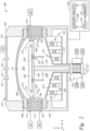
- FIG. 1 is a schematic cross sectional side view of a process chamber 100 according to one embodiment.
- the process chamber 100 may be a process chamber for performing any thermal process, such as an epitaxial process. It is contemplated that while a process chamber for epitaxial process is shown and described, the concept of the present disclosure is also applicable to other process chamber that is capable of providing a controlled thermal cycle that heats the substrate for processes such as, for example, thermal annealing, thermal cleaning, thermal chemical vapor deposition, thermal oxidation and thermal nitridation, regardless of whether the heating elements are provided at the top, bottom, or both of the process chamber.
- the process chamber 100 may be used to process one or more substrates, including the deposition of a material on a deposition surface 122 of a substrate 110.
- the process chamber 100 may include a first dome 112, a second dome 114, and a substrate support 102 disposed between the first dome 112 and the second dome 114.
- the substrate support 102 may include a susceptor 124 for supporting the substrate 110 and a susceptor support 126 for supporting the susceptor 124.
- the first dome 112 and the second dome 114 may be constructed from an optically transparent material, such as quartz.
- the substrate 110 can be brought into the process chamber 100 through a loading port 128 and positioned on the susceptor 124.
- the susceptor 124 may be made of SiC coated graphite.
- the susceptor support 126 may be rotated by a motor (not shown), which in turn rotates the susceptor 124 and the substrate 110.
- the process chamber 100 may further include a first plurality of heating elements 106, such as radiant heating lamps, disposed below the second dome 114 for heating the substrate 110 from below the substrate 110.
- the process chamber 100 may also include a second plurality of heating elements 104, such as radiant heating lamps, disposed over the first dome 112 for heating the substrate 110 from above the substrate 110.
- the first and second plurality of heating elements 104, 106 provide infrared radiant heat to the substrate though the first dome 112 and the second dome 114, respectively.
- the first and second domes 112, 114 may be transparent to the infrared radiation, defined as transmitting at least 95% of infrared radiation.
- the process chamber 100 may also include one or more temperature sensors 130, such as optical pyrometers, which measure temperatures within the process chamber 100 and on the surface 122 of the substrate 110.
- the one or more temperature sensors 130 may be disposed on a support member 132 that is disposed on a lid 116.
- a reflector 118 may be placed outside the first dome 112 to reflect infrared light radiating from the substrate 110 and the first dome 112 back towards the substrate 110.
- One or more high-energy radiant source assemblies 108 such as focused high-energy radiant source assemblies, for example laser source assemblies, may be disposed on the support member 132.
- the one or more high-energy radiant source assemblies 108 may produce one or more high-energy radiant beams 134, such as focused high-energy radiant beams, for example laser beams, which form a beam spot on the surface 122 of the substrate 110 in order to perform localized heating of the substrate 110.
- the one or more high-energy radiant beams 134 may go through an opening 120 formed in an annular portion 136 of the reflector 118, and the first dome 112 may be transparent to the high-energy radiant beams (transmitting at least 95% of the radiation of the high-energy radiant beam 134).
- the distance D 1 one high-energy radiant beam 134 of the one or more beams 134 travels from a lens ( Figure 3 ) to the surface 122 of the substrate 110 is about 400 mm, and the distance D2 the one high-energy radiant beam 134 of the one or more beams 134 travels from the first dome 112 to the surface 122 of the substrate 110 is about 76 mm.
- the substrate 110 may be heated to a predetermined temperature, such as less than about 750 degrees Celsius. Despite the precise control of heating the substrate 110, one or more regions on the substrate 110 may experience temperature non-uniformity, such as about 2-5 degrees Celsius lower than rest of the substrate 110.
- the temperature non-uniformity leads to film thickness non-uniformity, such as thickness non-uniformity of one percent or more, for a film deposited on the substrate in the one or more regions.
- the one or more high-energy radiant source assemblies 108 are used to locally heat the one or more regions on the substrate 110.
- the localized heating by the one or more high-energy radiant source assemblies 108 may be over an annular region at a certain radius of the substrate 110.
- the annular region is at about 50 mm radius.
- the one or more high-energy radiant source assemblies 108 may be movably disposed on the support member 132, such as movably disposed on a track ( Figure 8 ) disposed along a radial direction on the support member 132, and the one or more high-energy radiant source assemblies 108 may be movable along the track in order to locally heat any cold regions on the substrate 110 during operation.
- multiple high-energy radiant source assemblies 108 ( Figures 8 and 9 ) are utilized to simultaneously heat multiple cold regions on the substrate 110.
- FIGS 2 and 3 illustrate a schematic sectional view of a process chamber 200 according to another embodiment.
- the process chamber 200 may be used as an epitaxial deposition chamber, a rapid thermal process chamber, or other thermal treatment chamber.
- the process chamber 200 may be used to process one or more substrates, including the deposition of a material on an upper surface of a substrate 202, heating of a substrate 202, etching of a substrate 202, or combinations thereof.
- the process chamber 200 generally includes a chamber wall 103, and an array of radiant heating lamps 204 for heating, among other components, a susceptor 206 disposed within the process chamber 200. As shown in Figure 2 and Figure 3 , an array of radiant heating lamps 204 may be disposed below the susceptor 206.
- an array of radiant heating lamps 204 may be disposed below and/or above the susceptor 206.
- the radiant heating lamps 204 may provide a total lamp power of between about 10KW and about 60KW.
- the radiant heating lamps 204 may heat the substrate 202 to a temperature of between about 500 degrees Celsius and about 900 degrees Celsius.
- the susceptor 206 may be a disk-like substrate support as shown, or may include a ring-like substrate support (not shown), which supports the substrate from the edge of the substrate, which exposes a backside of the substrate 202 to heat from the radiant heating lamps 204.
- the susceptor 206 may be formed from silicon carbide or graphite coated with silicon carbide to absorb radiant energy from the lamps 204 and conduct the radiant energy to the substrate 202, thus heating the substrate 202.
- the susceptor 206 is located within the process chamber 200 between a first transmissive member 208, which may be a dome, and a second transmissive member 210, which may be a dome.
- Each of the first transmissive member 208 and/or the second transmissive member 210 may be convex and/or concave. In some embodiments, each of the first transmissive member 208 and/or the second transmissive member 210 may be transparent.
- the first transmissive member 208 may be disposed between the chamber wall 103 and the susceptor 206.
- an array of radiant heating lamps 204 may be disposed outside of the internal region 211 of the process chamber 200 and/or above the first transmissive member 208, for example, a region 149 defined between the first transmissive member 208 and a reflector 254 (discussed infra ).
- the substrate 202 can be transferred into the process chamber 200 and positioned onto the susceptor 206 through a loading port (not shown) formed in the base ring 212.
- a process gas inlet 214 and a gas outlet 216 may be provided in the base ring 212.
- the susceptor 206 includes a shaft or stem 218 that is coupled to a motion assembly 220.
- the motion assembly 220 includes one or more actuators and/or adjustment devices that provide movement and/or adjustment of the stem 218 and/or the susceptor 206 within the internal region 211.
- the motion assembly 220 may include a rotary actuator 222 that rotates the susceptor 206 about a longitudinal axis A of the process chamber 200.
- the longitudinal axis A may include a center of an X-Y plane of the process chamber 200.
- the motion assembly 220 may include a vertical actuator 224 to lift and lower the susceptor 206 in the Z direction.
- the motion assembly 220 may include a tilt adjustment device 226 that is used to adjust a planar orientation of the susceptor 206 in the internal region 211.
- the motion assembly 220 may also include a lateral adjustment device 228 that is utilized to adjust the positioning of the stem 218 and/or the susceptor 206 side to side within the internal region 211.
- the lateral adjustment device 228 is utilized to adjust positioning of the stem 218 and/or the susceptor 206 in the X and/or Y direction while the tilt adjustment device 226 adjusts an angular orientation ( ⁇ ) of the stem 218 and/or the susceptor 206.
- the motion assembly 220 includes a pivot mechanism 230.
- the pivot mechanism 230 is utilized to allow the motion assembly 220 to move the stem 218 and/or the susceptor 206 at least in the angular orientation ( ⁇ ) to reduce stresses on the second transmissive member 210.
- the susceptor 206 is shown in an elevated processing position but may be lifted or lowered vertically by the motion assembly 220 as described above.
- the susceptor 206 may be lowered to a transfer position (below the processing position) to allow lift pins 232 to contact the second transmissive member 210.
- the lift pins 232 extend through holes 207 in the susceptor 206 as the susceptor 206 is lowered, and the lift pins 232 raise the substrate 202 from the susceptor 206.
- a robot (not shown) may then enter the process chamber 200 to engage and remove the substrate therefrom though the loading port.
- a new substrate 202 may be loaded onto the lift pins 232 by the robot, and the susceptor 206 may then be actuated up to the processing position to place the substrate 202, with its device side 250 facing up.
- the lift pins 232 include an enlarged head allowing the lift pins 232 to be suspended in openings by the susceptor 206 in the processing position.
- stand-offs 234 coupled to the second transmissive member 210 are utilized to provide a flat surface for the lift pins 232 to contact.
- the stand-offs provide one or more surfaces parallel to the X-Y plane of the process chamber 200 and may be used to prevent binding of the lift pins 232 that may occur if the end thereof is allowed to contact the curved surface of the second transmissive member 210.
- the stand-offs 234 may be made of an optically transparent material, such as quartz, to allow energy from the lamps 204 to pass therethrough.
- the susceptor 206 while located in the processing position, divides the internal volume of the process chamber 200 into a process gas region 236 that is above the susceptor 206, and a purge gas region 238 below the susceptor 206.
- the susceptor 206 is rotated during processing by the rotary actuator 222 to minimize the effect of thermal and process gas flow spatial anomalies within the process chamber 200 and thus facilitates uniform processing of the substrate 202.
- the susceptor 206 may rotate at between about 5 RPM and about 100 RPM, for example, between about 10 RPM and about 50 RPM.
- the susceptor 206 is supported by the stem 218, which is generally centered on the susceptor 206 and facilitates movement of the susceptor 206 substrate 202 in a vertical direction (Z direction) during substrate transfer, and in some instances, processing of the substrate 202.
- the central portion of the first transmissive member 208 and the bottom of the second transmissive member 210 are formed from an optically transparent material such as quartz.
- the thickness and the degree of curvature of the first transmissive member 208 may be selected to provide a flatter geometry for uniform flow in the process chamber.
- One or more lamps can be disposed adjacent to and beneath the second transmissive member 210 in a specified manner around the stem 218.
- the radiant heating lamps 204 may be independently controlled in zones in order to control the temperature of various regions of the substrate 202 as the process gas passes thereover, thus facilitating the deposition of a material onto the upper surface of the substrate 202.
- the deposited material may include silicon, doped silicon, germanium, doped germanium, silicon germanium, doped silicon germanium, gallium arsenide, gallium nitride, or aluminum gallium nitride.
- the radiant heating lamps 204 may include a radiant heat source, depicted here as a lamp bulb 241, and may be configured to heat the substrate 202 to a temperature within a range of about 200 degrees Celsius to about 1,600 degrees Celsius.
- Each lamp bulb 241 can be coupled to a power distribution board, such as printed circuit board (PCB) 252, through which power is supplied to each lamp bulb 241.
- PCB printed circuit board
- a standoff may be used to couple the lamp bulb 241 to the power distribution board, if desired, to change the arrangement of lamps.
- the radiant heating lamps 204 are positioned within a lamphead 245 which may be cooled during or after processing by, for example, a cooling fluid introduced into channels 249 located between the radiant heating lamps 204.
- a circular shield 246 may be optionally disposed around the susceptor 206 and coupled to a sidewall of the chamber body 248.
- the shield 246 prevents or minimizes leakage of heat/light noise from the lamps 204 to the device side 250 of the substrate 202 in addition to providing a pre-heat zone for the process gases.
- the shield 246 may be made from CVD SiC, sintered graphite coated with SiC, grown SiC, opaque quartz, coated quartz, or any similar, suitable material that is resistant to chemical breakdown by process and purge gases.
- the shield 246 is coupled to a liner 263 disposed on the base ring 212.
- Substrate temperature is measured by sensors configured to measure temperatures at the bottom of the susceptor 206.
- the sensors may be pyrometers (not shown) disposed in ports formed in the lamphead 245. Additionally or alternatively, one or more sensors 253, such as a pyrometer, may be directed to measure the temperature of the device side 250 of the substrate 202.
- a reflector 254 may be optionally placed outside the first transmissive member 208 to reflect infrared light that is radiating off the substrate 202 and redirect the energy back onto the substrate 202.
- the reflector 254 may be secured to the first transmissive member 208 using a clamp ring 256.
- the reflector 254 may be disposed adjacent the chamber wall 103. In some embodiments, the reflector may be coupled to the chamber wall 103.
- the reflector 254 can be made of a metal such as aluminum or stainless steel.
- the sensors 253 may be disposed through the reflector 254 to receive radiation from the device side 250 of the substrate 202.
- Process gas supplied from a process gas supply source 251 is introduced into the process gas region 236 through the process gas inlet 214 formed in the sidewall of the base ring 212.
- the process gas inlet 214 is configured to direct the process gas in a generally radially inward direction.
- the process gas inlet 214 may be a cross-flow gas injector.
- the cross-flow gas injector is positioned to direct the process gas across a surface of the susceptor 206 and/or the substrate 202.
- the susceptor 206 is located in the processing position, which is adjacent to and at about the same elevation as the process gas inlet 214, thus allowing the process gas to flow generally along flow path 273 across the upper surface of the susceptor 206 and/or substrate 202.
- the process gas exits the process gas region 236 (along flow path 275) through the gas outlet 216 located on the opposite side of the process chamber 200 as the process gas inlet 214. Removal of the process gas through the gas outlet 216 may be facilitated by a vacuum pump 257 coupled thereto.
- Purge gas supplied from a purge gas source 262 is introduced to the purge gas region 238 through a purge gas inlet 264 formed in the sidewall of the base ring 212.
- the purge gas inlet 264 is disposed at an elevation below the process gas inlet 214. If the circular shield 246 is used, the circular shield 246 may be disposed between the process gas inlet 214 and the purge gas inlet 264. In either case, the purge gas inlet 264 is configured to direct the purge gas in a generally radially inward direction. The purge gas inlet 264 may be configured to direct the purge gas in an upward direction.
- the susceptor 206 is located at a position such that the purge gas flows generally along flow path 265 across a back side of the susceptor 206.
- the purge gas exits the purge gas region 238 (along flow path 266) and is exhausted out of the process chamber through the gas outlet 216 located on the opposite side of the process chamber 200 as the purge gas inlet 264.
- the process chamber 200 further includes a high-energy radiant source assembly 270, such as a focused high-energy radiant source assembly, for example a laser system assembly.
- the high-energy radiant source assembly 270 may be coupled to the process chamber 200.
- the process chamber 200 may include a plurality of high-energy radiant source assemblies 270, for example two or more assemblies 270 coupled to the process chamber 200.
- FIG 4 schematically illustrates a perspective view of the high-energy radiant source assembly 270 of Figure 2 and Figure 3 .
- the high-energy radiant source assembly 270 includes a source head 272, a source 274, and a fiber cable 276.
- the source 274 may be operatively connected to the source head 272 via the fiber cable 276.
- the high-energy radiant source assembly 270 may be a laser system assembly, such as a diode laser system assembly.
- the fiber cable 276 may include at least one diode.
- the fiber cable 276 may include a plurality of diodes.
- the high-energy radiant source assembly 270 may include a plurality of source heads 272 operatively connected to the source 274.
- the plurality of source heads 272 may be operatively connected to the source 274 via one or more fiber cables 276.
- the source head 272 may be coupled with the processing chamber 200 adjacent the upper lamp module, as shown in Figure 2 , and/or adjacent the lift pins 232.
- the source head 272 may secure an end of the fiber cable 276 in a fixed position such that the position of the high-energy radiant beam, such as a laser beam, is controlled.
- the high-energy radiant source assembly 270 may further include a mounting bracket 278.
- the mounting bracket 278 may be coupled to the processing chamber 200.
- the source head 272 may be coupled to the mounting bracket 278.
- the high-energy radiant source assembly 270 may further include a cover plate 280, the reflector 254, and a reflector member 284.
- the reflector 254 may be coupled to the chamber wall 103 and/or the mounting bracket 278. In some embodiments, the reflector 254 may be a circular disk; however, it is contemplated that the reflector 254 may be of any suitable shape.
- the reflector member 284 may be circular.
- the reflector member 284 may have an outer wall 294, a first edge 295, and a second edge 296.
- the outer wall 294, the first edge 295, and/or the second edge 296 may be circular in shape, ring like, or other suitable shapes.
- the first edge 295 may be disposed at a first end 297 of the reflector member 284 and the second edge 296 may disposed at a second end 298 of the reflector member 284, wherein the first edge is opposite the second edge 296.
- the first edge 295 and the second edge 296 may be substantially perpendicular to the outer wall 294.
- the second edge 296 may include at least one hole 199 bored therethrough for allowing light through the reflector member 284.
- the source head 272 may be positioned such that light from the source head 272 enters through the hole 199 toward the substrate 202 and/or the susceptor 206.
- the reflector member 284 may be coupled to the reflector 254. In some embodiments, the reflector member 284 may be coupled to the first edge 295 of the reflector member. In some embodiments, the reflector member 284 may be coupled to the reflector member 284 via a screw connection, a bolt connection, and/or any other suitable connection means.
- the cover plate 280 may be a circular cover plate 280 or a disk-shaped cover plate 280; however it is contemplated that the cover plate 280 may be of any suitable shape.
- the cover plate 280 may have a diameter less than a diameter of the reflector 254.
- the cover plate 280 may be disposed between the mounting bracket 278 and the reflector 254.
- the cover plate 280 may be coupled to the reflector 254.
- the cover plate 280 may be coupled to the reflector 254 with a bolted connection, a screw connection, and/or any other suitable connection means.
- the high-energy radiant source assembly 270 is positioned to direct high-energy radiant beam at a region of the susceptor 206 between about 90mm and about 130mm, for example between about 100mm and about 120mm, from a central area C of the susceptor 206.
- FIG. 5 schematically illustrates an enlarged view of the high-energy radiant source assembly 270 of Figure 4 .
- the mounting bracket 278 may be coupled to the cover plate 280.
- the mounting bracket 278 may be coupled to the cover plate 280 via a bolt mechanism.
- the mounting bracket 278 is coupled from a bottom side of the mounting bracket 278 to the cover plate 280 via a fastening mechanism 504, which may include a bolt.
- the mounting bracket 278 may be a "C" shaped mounting bracket 278 or an "L" shaped mounting bracket 278; however, it is contemplated that the mounting bracket 278 may be of any suitable shape.
- the mounting bracket 278 may include a first arm 286 which extends parallel to a surface of the cover plate 280, and/or a second arm 288 which extends perpendicular to a surface of the cover plate 280.
- the source head 272 may be coupled to the mounting bracket 278. In some embodiments, the source head 272 may be coupled to the first arm 286 of the mounting bracket 278, such that the source head 272 is raised relative to the cover plate 280.
- the first arm 286 of the mounting bracket 278, which, in certain embodiments, is coupled to the source head 272, may be tilted such that the first arm 286 of the mounting bracket 278 and the second arm 288 of the mounting bracket are not perpendicular.
- the first arm 286 of the mounting bracket 278 may be tilted at an angle of between about -4 degrees and about 4 degrees relative to the surface 282 of the cover plate 280.
- the source head 272 may be tilted 2 degrees relative to the surface 282 of the cover plate 280 and/or the surface of the susceptor 206.
- the surface 282 of the cover plate 280 may be parallel to a horizontal axis D of the susceptor 206.
- the first arm 286 of the mounting bracket 278 has a first central axis A and the second arm 288 of the mounting bracket 278 has a second central axis B.
- the first central axis A is not orthogonal to the second central axis B.
- the susceptor 206 has a horizontal axis D.
- the first central axis A of the first arm 286 of the mounting bracket 278 is not parallel to the horizontal axis D of the susceptor 206.
- the mounting bracket 278 may include a third arm 189.
- the third arm 189 of the mounting bracket 278 may have a central axis E.
- the central axis E of the third arm 189 may be parallel to the surface 282 of the cover plate 280.
- the third arm 189 may be coupled to the cover plate 280.
- the third arm 189 may be coupled to the cover plate 280 by a bolting mechanism and/or any other suitable connection mechanism.
- the second arm 288 of the mounting bracket 278 may be tilted, such that the central axis B of the second arm 288 is not perpendicular to the central axis E of the third arm 189.
- the central axis B of the second arm 288 may be tilted between about -4 degrees and about 4 degrees from an axis perpendicular to the central axis E of the third arm 189.
- the central axis A of the first arm 286 may be perpendicular to the central axis B of the second arm.
- tilting of the of the first arm 286 of the mounting bracket 278 and the source head 272 may decrease and/or prevent back shot of the light to the laser head 272.
- tilting of the source head 272 may position the high-energy radiant source assembly 270 to direct light at a region of the susceptor 206 between about 90mm and about 130mm, for example between about 100mm and about 120mm, from the central area C of the susceptor 206.
- Positioning of the high-energy radiant source assembly 270 and directing light at the region of the susceptor 206 between about 90mm and about 130mm from the central area C of the susceptor 206 may direct the light onto an area of the susceptor 206 and/or substrate 202 that is coupled with at least one lift pin 232.
- the high-energy radiant source assembly 270 may further include a lens holder 290.
- the lens holder 290 may be coupled to the mounting bracket 278.
- the lens holder 290 may be coupled to the second arm 288 of the mounting bracket 278.
- the lens holder 290 may be coupled to the mounting bracket 278 with a bolt connection, a screw connection, and/or any other suitable connection mechanism.
- the lens holder 290 is coupled to the mounting bracket 278 with screw 502.
- the lens holder 290 may extend outward from the mounting bracket 278 such that the lens holder 290 is disposed between the source head 272 and the cover plate 280.
- the lens holder 290 may be tilted at the same angle or at an angle substantially similar to the tilt angle of the source head 272. As such, a central axis F of the lens holder 290 may be substantially parallel to a central axis G of the source head 272.
- the lens holder 290 may include a lens 292.
- the lens 292 may be a telecentric lens.
- the telecentric lens 292 may defocus the light from the laser head 272 into a beam.
- the telecentric lens 292 may collimate the light.
- the lens 292 may focus the light from the source head 272 into a beam having a diameter of between about 2mm and about 10mm, for example between about 4mm and about 8mm.
- the lens holder 290 may include one or more optical elements.
- the source 274 may be offsite or onsite.
- the source may generate energy, for example light.
- the source 274 may be a diode laser source.
- the diodes may be electrically pumped. Recombination of the electrons and holes created by the applied current may introduce an optical gain. Reflection from the ends of a crystal may form an optical resonator, although the resonator may be external.
- the source 274 may be a fiber laser source.
- the fiber laser source may be a solid-state laser or a laser amplifier in which the light is guided due to a total internal reflection in a single mode optical fiber.
- the guiding of the light may allow for long gain regions.
- wave guiding properties of the fiber laser reduce thermal distortion of the light beam. Erbium and/or ytterbium ions may be active species in the fiber laser.
- the source 274 may provide a laser power of between about 20 watts and about 200 watts.
- the source 274 may be a source of laser light.
- the fiber cable 276 may be a light pipe to transmit the laser light into the process chamber 200. Additionally, in some embodiments, the fiber cable 276 may be a single pass amplifier.
- the source 274 may be a source of seed photons.
- the fiber cable 276 is a lasing medium comprising at least one diode.
- the diode may be inside the fiber cable 276.
- the fiber cable 276 may be the oscillator.
- the source 274 is a source of seed photons configured to start the stimulated emission of photons in the fiber cable 276 or in other such lasing mediums.
- the source 274 and the fiber cable 276, together, may comprise the laser.
- the substrate 202 may be loaded onto the lift pins 232 by the robot, and the susceptor 206 may then be actuated up to the processing position to place the substrate 202, with its device side 250 facing up.
- the lift pins 232 include an enlarged head allowing the lift pins 232 to be suspended in openings by the susceptor 206 in the processing position.
- the high-energy radiant source assembly 270 may provide localized heating to eliminate cold spots due to the lift pins 232. As such, the high-energy radiant source assembly 270 may focus a beam of the light to between about 2mm and about 20mm, for example to about 10mm.
- the high-energy radiant source assembly 270 may focus the light beam while the substrate 202 is rotating within the process chamber 200. Heating from the laser beam may cause a reduction in the resistivity (Rs) profile of the implant substrate 202 when annealed, as an increase in temperature lowers resistivity.
- Rs resistivity
- the high-energy radiant source assembly 270 may be directed to proper locations and operated at specific timings.
- the lift pins 232 operate at about 32RPM and move at a speed of about 380mm/s.
- timing control is calculated to be less than about 2.5ms.
- focusing of the light may be performed at specific timing intervals.
- a shutter with a speed similar to the speed of the susceptor 206 may be utilized as necessary.
- a laser with a 6 microsecond raise time may be utilized.
- the high-energy radiant source assembly 270 may provide a pulsed light beam such that the high-energy radiant source assembly 270 is on and functioning 0.5ms before the lift pin 232 is in contact with the substrate 202. It is contemplated that other time intervals may be utilized. In some embodiments, the high-energy radiant source assembly 270 may be turned off 0.5ms after the substrate passes the light of the high-energy radiant source assembly 270.
- a source head 272 on a moveable track may be utilized to ensure appropriate tuning of the substrate 202.
- the moveable track may allow the source head 272 to sweep across the substrate 202, thus allowing for gross adjustments in a predetermined pattern.
- the source head 272 may move from the outer circumference radially inward, however other embodiments, such as movement from the origin radially outward, etc.
- the high-energy radiant source assembly 270 is turned to the on position when the lift pin 232 is approximately in line with and/or at the focus position. As such, the motion of the lift pin 232 is synchronized with the high-energy radiant source assembly 270.
- a flag may be built on the susceptor 206 to indicate the location of the lift pin 232.
- the flag may have a width of between about 0.1 degree and about 1.0 degree.
- the flag may be machined and/or may be mounted to or coupled to the susceptor 206.
- a delay in the flag signal may be introduced to ease the mounting or coupling tolerance. The delay may be adjusted in order to improve accuracy of the high-energy radiant source assembly 270, thus improving accuracy of the light with respect to the locations of the lift pins 232.
- the flag may be a homing flag and/or an optical sensor.
- the flag may trigger an optical switch associated with a home location on the substrate 202.
- the flag may be machined into or coupled to the rotation assembly, such as the susceptor.
- a rotation encoder may be utilized to sync the high-energy radiant source assembly 270.
- the encoder may be a range based encoder.
- the encoder may me controlled by a controller 250, described infra .
- the encoder may have about a 0.03 degree resolution or better in order to achieve less than 1mm accuracy, and may be pulled at less than, in some embodiments, for example, 2.5ms. In other embodiments, the encoder may be pulled at a rate of 1ms.
- an imaging process may be used to detect features on the susceptor 206 and predict when to fire the high-energy radiant source assembly 270.
- the imaging process may be completed with less than a 2.5ms turnaround time.
- an algorithm may be determined and controlled by the controller 250 to predict and/or determine when to fire the high-energy radiant source assembly 270.
- the above-described process chamber 200 can be controlled by a processor based system controller, such as controller 250, shown in Figures 2 and 3 .
- the controller 250 may be configured to control flow of various precursor and process gases and purge gases from gas sources, during different operations of a substrate process sequence.
- the controller 250 may be configured to control a firing of the high-energy radiant source assembly 270, predict an algorithm for firing the high-energy radiant source assembly 270, control operation of the flag and/or flag signal, and/or encode or sync the high-energy radiant source assembly 270, among other controller operations.
- the controller 250 includes a programmable central processing unit (CPU) 252 that is operable with a memory 255 and a mass storage device, an input control unit, and a display unit (not shown), such as power supplies, clocks, cache, input/output (I/O) circuits, and the like, coupled to the various components of the process chamber 200 to facilitate control of the substrate processing.
- the controller 250 also includes hardware for monitoring substrate processing through sensors in the process chamber 200, including sensors monitoring the precursor, process gas and purge gas flow. Other sensors that measure system parameters such as substrate temperature, chamber atmosphere pressure and the like, may also provide information to the controller 250.
- the CPU 252 may be one of any form of general purpose computer processor that can be used in an industrial setting, such as a programmable logic controller (PLC), for controlling various chambers and sub-processors.
- the memory 255 is coupled to the CPU 252 and the memory 255 is non-transitory and may be one or more of readily available memory such as random access memory (RAM), read only memory (ROM), floppy disk drive, hard disk, or any other form of digital storage, local or remote.
- Support circuits 258 are coupled to the CPU 252 for supporting the processor in a conventional manner.
- Charged species generation, heating, and other processes are generally stored in the memory 255, typically as a software routine.
- the software routine may also be stored and/or executed by a second CPU (not shown) that is remotely located from the hardware being controlled by the CPU 252.
- the memory 255 is in the form of computer-readable storage media that contains instructions, that when executed by the CPU 252, facilitates the operation of the process chamber 200.
- the instructions in the memory 255 are in the form of a program product such as a program that implements the method of the present disclosure.
- the program code may conform to any one of a number of different programming languages.
- the disclosure may be implemented as a program product stored on computer-readable storage media for use with a computer system.
- the program(s) of the program product define functions of the embodiments (including the methods described herein).
- Illustrative computer-readable storage media include, but are not limited to: (i) non-writable storage media (e.g., read-only memory devices within a computer such as CD-ROM disks readable by a CD-ROM drive, flash memory, ROM chips or any type of solid-state non-volatile semiconductor memory) on which information is permanently stored; and (ii) writable storage media (e.g., floppy disks within a diskette drive or hard-disk drive or any type of solid-state random-access semiconductor memory) on which alterable information is stored.
- non-writable storage media e.g., read-only memory devices within a computer such as CD-ROM disks readable by a CD-ROM drive, flash memory, ROM chips or any type of solid-state non-volatile semiconductor memory
- writable storage media e.g., floppy disks within a diskette drive or hard-disk drive or any type of solid-state random-access semiconductor memory
- FIG 6 is a perspective view of the high-energy radiant source assembly 108 ( Figure 1 ) according to one embodiment.
- one high-energy radiant source assembly 108 of the one or more assemblies 108 may include a high-energy radiant source 602 and a bracket 610 for supporting components of the high-energy radiant source assembly 108.
- the high-energy radiant source assembly 108 may further include a cage plate 608 disposed on the bracket 610 for securing a fiber connector 606.
- the high-energy radiant source 602 is connected to the fiber connector 606 via a fiber 604.
- the high-energy radiant source 602 may be any suitable high-energy radiant source for producing radiant energy, such as focused radiant energy, at a power capable of increasing the temperature of the substrate 110 ( Figure 1 ) by 2-5 degrees Celsius during a deposition process, such as an epitaxial deposition.
- the focused high-energy may have a wavelength in the visible range.
- the high-energy radiant source 602 is a laser source including two laser diodes each having at least 50 W output power for a total output power of at least 100 W and a wavelength of about 810 nm.
- the high-energy radiant source 602 is a vertical cavity surface emitting laser (VCSEL) including 33 chips in series having a total output power of 264 W (each chip has an output power of 8 W).
- the length of the fiber 604 may be about 15 m.
- the high-energy radiant source 602 is disposed on the bracket 610.
- the high-energy radiant source assembly 108 may further include an optic holder 612 for holding one or more lenses, such as an aspheric lens ( Figure 7 ).
- the high-energy radiant source assembly 108 may be disposed on a support block 614 that is bolted to the support member 132. Alternatively, the high-energy radiant source assembly 108 may be disposed on a track along a radial direction of the substrate 110 ( Figure 8 ).
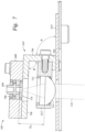
- FIG 7 is an enlarged schematic cross sectional side view of the high-energy radiant source assembly 108 according to one embodiment.
- the cage plate 608 may include two retainer rings 708, 710 for securing the fiber connector 606.
- the optic holder 612 may include a retainer ring 712 for securing a lens 714, such as an aspheric lens.
- the bracket 610 may include a first portion 702 coupled to the support block 614, a second portion 704 at an angle A with respect to the first portion 702, and a third portion 706 at an angle B with respect to the second portion 704.
- the optic holder 612 may be coupled to the second portion 704 and the cage plate 608 may be coupled to the third portion 706.
- the angle B is about 90 degrees and the angle A is either an acute or obtuse angle that is not 90 degrees so the second portion 704 is not substantially perpendicular to the surface 122 of the substrate 110 ( Figure 1 ).
- the angle A is about 92 degrees and the angle B is about 90 degrees, so the lens 714 has a 2° tilt with respect to the third portion 706 to prevent back reflections into the fiber 604 which could damage the high-energy radiant source 602.
- the angle A is about 90 degrees and the angle B is either an acute or obtuse angle that is not 90 degrees.
- the acute or obtuse angle A or B can be used to determine the location on the substrate 110 of the beam spot of the one or more high-energy radiant beams 134.
- first, second, and third portions 702, 704, 706 are a single piece of material, and the angles A, B are set and are not adjustable. In another embodiment, the first, second, and third portions 702, 704, 706 are made of different pieces of materials, and the angles A, B can be adjusted.
- the high-energy radiant beam, such as a focused high-energy radiant beam, for example a laser beam, out of the fiber 604 has a diameter of about 800 micrometers that is re-imaged onto the substrate 110 at 17x magnification by the lens 714, so the beam spot on the substrate 110 has a diameter of about 10 mm.
- the laser beam out of the fiber exits at a divergence of about 0.17 NA.
- the distance D 3 one focused high-energy radiant beam 134 of the one or more beams 134 travels from the fiber connector 606 to the lens 714 is about 18 mm.
- the transparent material of the first dome 112 may cause a slight shift of the beam spot on the substrate which can be compensated by adjusting the angle A or B.
- a small percentage of the high-energy radiant beam may be reflected by the first dome 112. In one embodiment, about 7 W of power is reflected by the first dome and the total output power of the high-energy radiant beam 134 is about 90 W.
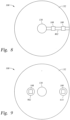
- Figure 8 is a schematic top view of the process chamber 100 of Figure 1 according to one embodiment.
- the process chamber 100 includes the one or more temperature sensors 130 supported by the support member 132.
- a track 802 may be formed on the support member 132 in a radial direction, and the one or more high-energy radiant source assemblies 108 may be movably disposed on the track 802.
- the one or more high-energy radiant source assemblies 108 may be moved during or between processes in order to provide localized heating of various regions on the substrate 110.
- one high-energy radiant source assembly 108 is disposed on the track 802.
- more than two high-energy radiant source assemblies 108 are disposed on the track 802.
- Figure 9 is a schematic top view of the process chamber 100 of Figure 1 according to one embodiment.
- one high-energy radiant source assembly 108 is disposed on the support block 614 and a second high-energy radiant source assembly 108 is disposed on a support block 902.
- the support blocks 614, 902 may be disposed at different radial positions on the support member 132 to simultaneously heat different radial regions of the substrate 110.
- one high-energy radiant source assembly 108 is utilized, and in some embodiments, more than two high-energy radiant source assemblies 108 are utilized.
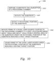
- Figure 10 schematically illustrates operations of a method 1000 for processing a substrate.
- the method 1000 may locally heat the substrate in an epitaxial deposition chamber.
- a substrate is disposed on a susceptor of a process chamber.
- the process chamber may be an epitaxy deposition chamber.
- the process chamber may be the process chamber 100 or the process chamber 200.
- the substrate is rotated.
- a rotational position of the substrate is detected.
- the rotational position of the substrate may be received by a controller and/or a sensor, which may be a camera or equivalent, or a thermal sensor.
- the rotational position may indicate the location and/or positioning of the substrate and/or the location and/or positioning of the susceptor within the processing chamber.
- the rotational position may also indicate the speed and/or timing of the substrate and/or susceptor within the processing chamber.
- a high-energy source such as a laser source
- the laser source may be a diode laser source.
- the high-energy source is coupled to the process chamber to a first location between about 100mm and about 120 from a central area of the substrate.
- the laser firing may be initiated from the diode laser source.
- the laser firing may last for any length of time and may be, in certain embodiments a constant firing and/or a pulsed firing.
- the firing of the laser may heat an area, portion, or specific region of the substrate, as described supra.
- firing the diode laser source may divert the light from the diode laser source to the first region of the chamber may allow the light from the laser source to tune and/or heat the first region.
- the first region of the chamber may include an area of a substrate coupled to a lift pin of the chamber. As such, the light may tune and/or heat the area of the substrate coupled to the lift pin in order to reduce a cold spot thereon.
- other types of lasers or laser sources may be utilized, for example a fiber laser, among others.
- the second target position may be received based on a rotational positioning of the susceptor and/or a rotational positioning of the substrate.
- the second target position may be received by the controller and/or a sensor.
- the second target position may indicate the location and/or positioning of the substrate and/or the location and/or positioning of the susceptor within the processing chamber.
- the second target position may also indicate the speed and/or timing of the substrate and/or susceptor within the processing chamber.
- the method 1000 may be repeated as the substrate and/or the susceptor is further rotated within the processing chamber.
- the substrate is optimally tuned, as the dip in resistivity is reduced, and cold spots on the substrate are appropriately compensated for, as shown in Figure 11 .
- located spot and area heating is applied to the substrate via the high-energy radiant source assembly in order to control the amount of energy going to the substrate.
- Certain and specific areas of the substrate may be tuned as the substrate rotates within the process chamber, thus alleviating a trough in the substrate profile and raising the profile of the substrate, as the high-energy radiant source assembly causes a narrow band of power to perform the localized heating.
- Benefits of the present disclosure include a reduction in the number of cold spots associated with a substrate. Reducing the temperature nonuniformities within a substrate further creates a substrate with a more uniform surface. A cost reduction is also realized in that there is an increase in substrate quality. Additional benefits include precise local heating of the substrate for ultra-fine tuning of temperature uniformity.
- an epitaxial deposition chamber which includes a high-energy radiant source assembly for providing localized heating of a substrate during processing.
- Energy may be focused to about a 10mm area during substrate rotation within the chamber in order to locally heat and tune specific locations of the substrate, such as locations adjacent a lift pin, at specifically timed intervals.
- Energy from the high-energy beam may provide a dip in a resistivity profile of an implant substrate when annealed.
- the high-energy radiant source assembly may be a diode laser system positioned to direct energy at a region of a susceptor between about 100mm and about 120mm from a central area of the susceptor.
Landscapes
- Physics & Mathematics (AREA)
- Engineering & Computer Science (AREA)
- Plasma & Fusion (AREA)
- Chemical & Material Sciences (AREA)
- Analytical Chemistry (AREA)
- Health & Medical Sciences (AREA)
- Toxicology (AREA)
- Electromagnetism (AREA)
- Optics & Photonics (AREA)
Abstract
Description
- Embodiments of the present disclosure generally relate to apparatus and methods for semiconductor processing, more particularly, to a thermal process chamber.
- Semiconductor substrates are processed for a wide variety of applications, including the fabrication of integrated devices and microdevices. During processing, the substrate is positioned on a susceptor within a process chamber. The susceptor is supported by a support shaft, which is rotatable about a central axis. Precise control over a heating source, such as a plurality of heating lamps disposed below and above the substrate, allows the substrate to be heated within very strict tolerances. The temperature of the substrate can affect the uniformity of the material deposited on the substrate.
- Despite the precise control of heating the substrate, it has been observed that valleys (lower deposition) are formed at certain locations on the substrate. Therefore, a need exists for an improved thermal process chamber in semiconductor processing.
- Embodiments of the present disclosure generally relate to apparatus and methods for semiconductor processing, more particularly, to a thermal process chamber. In one embodiment, a process chamber includes a first dome, a second dome, a substrate support disposed between the first dome and the second dome, a first plurality of heating elements disposed over the first dome, wherein the first dome is disposed between the first plurality of heating elements and the substrate support, and a high-energy radiant source assembly disposed over the first plurality of heating elements, wherein the high-energy radiant source assembly comprises a high-energy radiant source having a total output power of at least 100 W.
- In another embodiment, a process chamber includes a first dome, a second dome, a substrate support disposed between the first dome and the second dome, a first plurality of heating elements disposed over the first dome, wherein the first dome is disposed between the first plurality of heating elements and the substrate support, a support member disposed over the first plurality of heating elements, wherein the first plurality of heating elements are disposed between the first dome and the support member, and a first high-energy radiant source assembly disposed on the support member, wherein the high-energy radiant source assembly comprises a high-energy radiant source and a bracket for coupling the high-energy radiant source assembly to the support member.
- In another embodiment, a process chamber includes a first dome, a second dome, a substrate support disposed between the first dome and the second dome, a plurality of heating elements disposed over the first dome, wherein the first dome is disposed between the plurality of heating elements and the substrate support, a support member disposed over the first plurality of heating elements, wherein the first plurality of heating elements are disposed between the first dome and the support member, and a high-energy radiant source assembly movably disposed on a track formed on the support member, wherein the high-energy radiant source assembly comprises a high-energy radiant source.
- So that the manner in which the above recited features of the present disclosure can be understood in detail, a more particular description of the disclosure, briefly summarized above, may be had by reference to embodiments, some of which are illustrated in the appended drawings. It is to be noted, however, that the appended drawings illustrate only typical embodiments of this disclosure and are therefore not to be considered limiting of its scope, for the disclosure may admit to other equally effective embodiments.
-
Figure 1 is a schematic cross sectional side view of a process chamber according to one embodiment. -
Figure 2 is a schematic cross sectional side view of a process chamber according to another embodiment. -
Figure 3 is a schematic cross sectional side view of a process chamber according to another embodiment. -
Figure 4 is a schematic perspective view of a high-energy radiant source assembly according to embodiments described herein. -
Figure 5 is a schematic cross sectional side view of the high-energy radiant source assembly ofFigure 4 according to one embodiment. -
Figure 6 is a schematic perspective view of the high-energy radiant source assembly according to one embodiment. -
Figure 7 is an enlarged schematic cross sectional side view of the high-energy radiant source assembly ofFigure 6 according to one embodiment. -
Figure 8 is a schematic top view of the process chamber ofFigure 1 according to one embodiment. -
Figure 9 is a schematic top view of the process chamber ofFigure 1 according to another embodiment. -
Figure 10 illustrates operations of a method for processing a substrate according to embodiments described herein. -
Figure 11 illustrates a data plot providing test results for distance from origin of the substrate versus resistivity of the substrate. - To facilitate understanding, identical reference numerals have been used, where possible, to designate identical elements that are common to the figures. It is contemplated that elements disclosed in one embodiment may be beneficially utilized in other embodiments without specific recitation.
- Embodiments of the present disclosure generally relate to apparatus and methods for semiconductor processing, more particularly, to a thermal process chamber. The thermal process chamber may include a substrate support, a first plurality of heating elements disposed over the substrate support, and one or more high-energy radiant source assemblies disposed over the first plurality of heating elements. The one or more high-energy radiant source assemblies are utilized to provide local heating of cold regions on a substrate disposed on the substrate support during processing. Localized heating of the substrate improves temperature profile, which in turn improves deposition uniformity.
- A "substrate" or "substrate surface," as described herein, generally refers to any substrate surface upon which processing is performed. For example, a substrate surface may include silicon, silicon oxide, doped silicon, silicon germanium, germanium, gallium arsenide, glass, sapphire, and any other materials, such as metals, metal nitrides, metal alloys, and other conductive or semi-conductive materials, depending on the application. A substrate or substrate surface may also include dielectric materials such as silicon dioxide, silicon nitride, organosilicates, and carbon dopes silicon oxide or nitride materials. The substrate itself is not limited to any particular size or shape. Although the embodiments described herein are made with generally made with reference to a round 200mm or 300mm substrate, other shapes, such as polygonal, squared, rectangular, curved, or otherwise non-circular workpieces may be utilized according to the embodiments described herein.
-
Figure 1 is a schematic cross sectional side view of aprocess chamber 100 according to one embodiment. Theprocess chamber 100 may be a process chamber for performing any thermal process, such as an epitaxial process. It is contemplated that while a process chamber for epitaxial process is shown and described, the concept of the present disclosure is also applicable to other process chamber that is capable of providing a controlled thermal cycle that heats the substrate for processes such as, for example, thermal annealing, thermal cleaning, thermal chemical vapor deposition, thermal oxidation and thermal nitridation, regardless of whether the heating elements are provided at the top, bottom, or both of the process chamber. - The
process chamber 100 may be used to process one or more substrates, including the deposition of a material on adeposition surface 122 of asubstrate 110. Theprocess chamber 100 may include afirst dome 112, asecond dome 114, and asubstrate support 102 disposed between thefirst dome 112 and thesecond dome 114. Thesubstrate support 102 may include asusceptor 124 for supporting thesubstrate 110 and asusceptor support 126 for supporting thesusceptor 124. Thefirst dome 112 and thesecond dome 114 may be constructed from an optically transparent material, such as quartz. Thesubstrate 110 can be brought into theprocess chamber 100 through aloading port 128 and positioned on thesusceptor 124. Thesusceptor 124 may be made of SiC coated graphite. Thesusceptor support 126 may be rotated by a motor (not shown), which in turn rotates thesusceptor 124 and thesubstrate 110. - The
process chamber 100 may further include a first plurality ofheating elements 106, such as radiant heating lamps, disposed below thesecond dome 114 for heating thesubstrate 110 from below thesubstrate 110. Theprocess chamber 100 may also include a second plurality ofheating elements 104, such as radiant heating lamps, disposed over thefirst dome 112 for heating thesubstrate 110 from above thesubstrate 110. In one embodiment, the first and second plurality ofheating elements first dome 112 and thesecond dome 114, respectively. The first andsecond domes - In one embodiment, the
process chamber 100 may also include one ormore temperature sensors 130, such as optical pyrometers, which measure temperatures within theprocess chamber 100 and on thesurface 122 of thesubstrate 110. The one ormore temperature sensors 130 may be disposed on asupport member 132 that is disposed on alid 116. Areflector 118 may be placed outside thefirst dome 112 to reflect infrared light radiating from thesubstrate 110 and thefirst dome 112 back towards thesubstrate 110. One or more high-energyradiant source assemblies 108, such as focused high-energy radiant source assemblies, for example laser source assemblies, may be disposed on thesupport member 132. The one or more high-energyradiant source assemblies 108 may produce one or more high-energyradiant beams 134, such as focused high-energy radiant beams, for example laser beams, which form a beam spot on thesurface 122 of thesubstrate 110 in order to perform localized heating of thesubstrate 110. The one or more high-energyradiant beams 134 may go through anopening 120 formed in anannular portion 136 of thereflector 118, and thefirst dome 112 may be transparent to the high-energy radiant beams (transmitting at least 95% of the radiation of the high-energy radiant beam 134). In one embodiment, the distance D1 one high-energyradiant beam 134 of the one ormore beams 134 travels from a lens (Figure 3 ) to thesurface 122 of thesubstrate 110 is about 400 mm, and the distance D2 the one high-energyradiant beam 134 of the one ormore beams 134 travels from thefirst dome 112 to thesurface 122 of thesubstrate 110 is about 76 mm. - During operation, such as an epitaxial deposition, the
substrate 110 may be heated to a predetermined temperature, such as less than about 750 degrees Celsius. Despite the precise control of heating thesubstrate 110, one or more regions on thesubstrate 110 may experience temperature non-uniformity, such as about 2-5 degrees Celsius lower than rest of thesubstrate 110. The temperature non-uniformity leads to film thickness non-uniformity, such as thickness non-uniformity of one percent or more, for a film deposited on the substrate in the one or more regions. In order to improve temperature uniformity, which in turn improves film thickness non-uniformity, the one or more high-energyradiant source assemblies 108 are used to locally heat the one or more regions on thesubstrate 110. Since thesubstrate 110 is rotating during operation, the localized heating by the one or more high-energyradiant source assemblies 108 may be over an annular region at a certain radius of thesubstrate 110. In one embodiment, the annular region is at about 50 mm radius. In some embodiments, the one or more high-energyradiant source assemblies 108 may be movably disposed on thesupport member 132, such as movably disposed on a track (Figure 8 ) disposed along a radial direction on thesupport member 132, and the one or more high-energyradiant source assemblies 108 may be movable along the track in order to locally heat any cold regions on thesubstrate 110 during operation. In some embodiments, multiple high-energy radiant source assemblies 108 (Figures 8 and 9 ) are utilized to simultaneously heat multiple cold regions on thesubstrate 110. -
Figures 2 and3 illustrate a schematic sectional view of aprocess chamber 200 according to another embodiment. Theprocess chamber 200 may be used as an epitaxial deposition chamber, a rapid thermal process chamber, or other thermal treatment chamber. Theprocess chamber 200 may be used to process one or more substrates, including the deposition of a material on an upper surface of asubstrate 202, heating of asubstrate 202, etching of asubstrate 202, or combinations thereof. Theprocess chamber 200 generally includes achamber wall 103, and an array ofradiant heating lamps 204 for heating, among other components, asusceptor 206 disposed within theprocess chamber 200. As shown inFigure 2 andFigure 3 , an array ofradiant heating lamps 204 may be disposed below thesusceptor 206. As shown inFigure 3 , an array ofradiant heating lamps 204 may be disposed below and/or above thesusceptor 206. Theradiant heating lamps 204 may provide a total lamp power of between about 10KW and about 60KW. Theradiant heating lamps 204 may heat thesubstrate 202 to a temperature of between about 500 degrees Celsius and about 900 degrees Celsius. Thesusceptor 206 may be a disk-like substrate support as shown, or may include a ring-like substrate support (not shown), which supports the substrate from the edge of the substrate, which exposes a backside of thesubstrate 202 to heat from theradiant heating lamps 204. Thesusceptor 206 may be formed from silicon carbide or graphite coated with silicon carbide to absorb radiant energy from thelamps 204 and conduct the radiant energy to thesubstrate 202, thus heating thesubstrate 202. - The
susceptor 206 is located within theprocess chamber 200 between afirst transmissive member 208, which may be a dome, and asecond transmissive member 210, which may be a dome. Thefirst transmissive member 208 and thesecond transmissive member 210, along with abase ring 212 that is disposed between thefirst transmissive member 208 andsecond transmissive member 210, generally define aninternal region 211 of theprocess chamber 200. Each of thefirst transmissive member 208 and/or thesecond transmissive member 210 may be convex and/or concave. In some embodiments, each of thefirst transmissive member 208 and/or thesecond transmissive member 210 may be transparent. Thefirst transmissive member 208 may be disposed between thechamber wall 103 and thesusceptor 206. In some embodiments, an array ofradiant heating lamps 204 may be disposed outside of theinternal region 211 of theprocess chamber 200 and/or above thefirst transmissive member 208, for example, aregion 149 defined between thefirst transmissive member 208 and a reflector 254 (discussed infra). Thesubstrate 202 can be transferred into theprocess chamber 200 and positioned onto thesusceptor 206 through a loading port (not shown) formed in thebase ring 212. Aprocess gas inlet 214 and agas outlet 216 may be provided in thebase ring 212. - The
susceptor 206 includes a shaft or stem 218 that is coupled to amotion assembly 220. Themotion assembly 220 includes one or more actuators and/or adjustment devices that provide movement and/or adjustment of thestem 218 and/or thesusceptor 206 within theinternal region 211. For example, themotion assembly 220 may include arotary actuator 222 that rotates thesusceptor 206 about a longitudinal axis A of theprocess chamber 200. The longitudinal axis A may include a center of an X-Y plane of theprocess chamber 200. Themotion assembly 220 may include avertical actuator 224 to lift and lower thesusceptor 206 in the Z direction. Themotion assembly 220 may include atilt adjustment device 226 that is used to adjust a planar orientation of thesusceptor 206 in theinternal region 211. Themotion assembly 220 may also include alateral adjustment device 228 that is utilized to adjust the positioning of thestem 218 and/or thesusceptor 206 side to side within theinternal region 211. In embodiments including alateral adjustment device 228 and atilt adjustment device 226, thelateral adjustment device 228 is utilized to adjust positioning of thestem 218 and/or thesusceptor 206 in the X and/or Y direction while thetilt adjustment device 226 adjusts an angular orientation (α) of thestem 218 and/or thesusceptor 206. In one embodiment, themotion assembly 220 includes apivot mechanism 230. As thesecond transmissive member 210 is attached to theprocess chamber 200 by thebase ring 212, thepivot mechanism 230 is utilized to allow themotion assembly 220 to move thestem 218 and/or thesusceptor 206 at least in the angular orientation (α) to reduce stresses on thesecond transmissive member 210. - The
susceptor 206 is shown in an elevated processing position but may be lifted or lowered vertically by themotion assembly 220 as described above. Thesusceptor 206 may be lowered to a transfer position (below the processing position) to allowlift pins 232 to contact thesecond transmissive member 210. The lift pins 232 extend throughholes 207 in thesusceptor 206 as thesusceptor 206 is lowered, and the lift pins 232 raise thesubstrate 202 from thesusceptor 206. A robot (not shown) may then enter theprocess chamber 200 to engage and remove the substrate therefrom though the loading port. Anew substrate 202 may be loaded onto the lift pins 232 by the robot, and thesusceptor 206 may then be actuated up to the processing position to place thesubstrate 202, with itsdevice side 250 facing up. The lift pins 232 include an enlarged head allowing the lift pins 232 to be suspended in openings by thesusceptor 206 in the processing position. In one embodiment, stand-offs 234 coupled to thesecond transmissive member 210 are utilized to provide a flat surface for the lift pins 232 to contact. The stand-offs provide one or more surfaces parallel to the X-Y plane of theprocess chamber 200 and may be used to prevent binding of the lift pins 232 that may occur if the end thereof is allowed to contact the curved surface of thesecond transmissive member 210. The stand-offs 234 may be made of an optically transparent material, such as quartz, to allow energy from thelamps 204 to pass therethrough. - The
susceptor 206, while located in the processing position, divides the internal volume of theprocess chamber 200 into aprocess gas region 236 that is above thesusceptor 206, and apurge gas region 238 below thesusceptor 206. Thesusceptor 206 is rotated during processing by therotary actuator 222 to minimize the effect of thermal and process gas flow spatial anomalies within theprocess chamber 200 and thus facilitates uniform processing of thesubstrate 202. Thesusceptor 206 may rotate at between about 5 RPM and about 100 RPM, for example, between about 10 RPM and about 50 RPM. Thesusceptor 206 is supported by thestem 218, which is generally centered on thesusceptor 206 and facilitates movement of thesusceptor 206substrate 202 in a vertical direction (Z direction) during substrate transfer, and in some instances, processing of thesubstrate 202. - In general, the central portion of the
first transmissive member 208 and the bottom of thesecond transmissive member 210 are formed from an optically transparent material such as quartz. The thickness and the degree of curvature of thefirst transmissive member 208 may be selected to provide a flatter geometry for uniform flow in the process chamber. - One or more lamps, such as an array of the
radiant heating lamps 204, can be disposed adjacent to and beneath thesecond transmissive member 210 in a specified manner around thestem 218. Theradiant heating lamps 204 may be independently controlled in zones in order to control the temperature of various regions of thesubstrate 202 as the process gas passes thereover, thus facilitating the deposition of a material onto the upper surface of thesubstrate 202. While not discussed here in detail, the deposited material may include silicon, doped silicon, germanium, doped germanium, silicon germanium, doped silicon germanium, gallium arsenide, gallium nitride, or aluminum gallium nitride. - The
radiant heating lamps 204 may include a radiant heat source, depicted here as alamp bulb 241, and may be configured to heat thesubstrate 202 to a temperature within a range of about 200 degrees Celsius to about 1,600 degrees Celsius. Eachlamp bulb 241 can be coupled to a power distribution board, such as printed circuit board (PCB) 252, through which power is supplied to eachlamp bulb 241. A standoff may be used to couple thelamp bulb 241 to the power distribution board, if desired, to change the arrangement of lamps. In one embodiment, theradiant heating lamps 204 are positioned within alamphead 245 which may be cooled during or after processing by, for example, a cooling fluid introduced intochannels 249 located between theradiant heating lamps 204. - A
circular shield 246 may be optionally disposed around thesusceptor 206 and coupled to a sidewall of thechamber body 248. Theshield 246 prevents or minimizes leakage of heat/light noise from thelamps 204 to thedevice side 250 of thesubstrate 202 in addition to providing a pre-heat zone for the process gases. Theshield 246 may be made from CVD SiC, sintered graphite coated with SiC, grown SiC, opaque quartz, coated quartz, or any similar, suitable material that is resistant to chemical breakdown by process and purge gases. In some embodiments, theshield 246 is coupled to aliner 263 disposed on thebase ring 212. - Substrate temperature is measured by sensors configured to measure temperatures at the bottom of the
susceptor 206. The sensors may be pyrometers (not shown) disposed in ports formed in thelamphead 245. Additionally or alternatively, one ormore sensors 253, such as a pyrometer, may be directed to measure the temperature of thedevice side 250 of thesubstrate 202. Areflector 254 may be optionally placed outside thefirst transmissive member 208 to reflect infrared light that is radiating off thesubstrate 202 and redirect the energy back onto thesubstrate 202. Thereflector 254 may be secured to thefirst transmissive member 208 using aclamp ring 256. Thereflector 254 may be disposed adjacent thechamber wall 103. In some embodiments, the reflector may be coupled to thechamber wall 103. Thereflector 254 can be made of a metal such as aluminum or stainless steel. Thesensors 253 may be disposed through thereflector 254 to receive radiation from thedevice side 250 of thesubstrate 202. - Process gas supplied from a process
gas supply source 251 is introduced into theprocess gas region 236 through theprocess gas inlet 214 formed in the sidewall of thebase ring 212. Theprocess gas inlet 214 is configured to direct the process gas in a generally radially inward direction. As such, in some embodiments, theprocess gas inlet 214 may be a cross-flow gas injector. The cross-flow gas injector is positioned to direct the process gas across a surface of thesusceptor 206 and/or thesubstrate 202. During a film formation process, thesusceptor 206 is located in the processing position, which is adjacent to and at about the same elevation as theprocess gas inlet 214, thus allowing the process gas to flow generally alongflow path 273 across the upper surface of thesusceptor 206 and/orsubstrate 202. The process gas exits the process gas region 236 (along flow path 275) through thegas outlet 216 located on the opposite side of theprocess chamber 200 as theprocess gas inlet 214. Removal of the process gas through thegas outlet 216 may be facilitated by avacuum pump 257 coupled thereto. - Purge gas supplied from a
purge gas source 262 is introduced to thepurge gas region 238 through apurge gas inlet 264 formed in the sidewall of thebase ring 212. Thepurge gas inlet 264 is disposed at an elevation below theprocess gas inlet 214. If thecircular shield 246 is used, thecircular shield 246 may be disposed between theprocess gas inlet 214 and thepurge gas inlet 264. In either case, thepurge gas inlet 264 is configured to direct the purge gas in a generally radially inward direction. Thepurge gas inlet 264 may be configured to direct the purge gas in an upward direction. During a film formation process, thesusceptor 206 is located at a position such that the purge gas flows generally alongflow path 265 across a back side of thesusceptor 206. The purge gas exits the purge gas region 238 (along flow path 266) and is exhausted out of the process chamber through thegas outlet 216 located on the opposite side of theprocess chamber 200 as thepurge gas inlet 264. - The
process chamber 200 further includes a high-energyradiant source assembly 270, such as a focused high-energy radiant source assembly, for example a laser system assembly. The high-energyradiant source assembly 270 may be coupled to theprocess chamber 200. In some embodiments, theprocess chamber 200 may include a plurality of high-energyradiant source assemblies 270, for example two ormore assemblies 270 coupled to theprocess chamber 200. -
Figure 4 schematically illustrates a perspective view of the high-energyradiant source assembly 270 ofFigure 2 andFigure 3 . The high-energyradiant source assembly 270 includes asource head 272, asource 274, and afiber cable 276. Thesource 274 may be operatively connected to thesource head 272 via thefiber cable 276. In some embodiments, the high-energyradiant source assembly 270 may be a laser system assembly, such as a diode laser system assembly. Thefiber cable 276 may include at least one diode. In some embodiments, thefiber cable 276 may include a plurality of diodes. Furthermore, in some embodiments, the high-energyradiant source assembly 270 may include a plurality of source heads 272 operatively connected to thesource 274. The plurality of source heads 272 may be operatively connected to thesource 274 via one ormore fiber cables 276. In some embodiments, thesource head 272 may be coupled with theprocessing chamber 200 adjacent the upper lamp module, as shown inFigure 2 , and/or adjacent the lift pins 232. Thesource head 272 may secure an end of thefiber cable 276 in a fixed position such that the position of the high-energy radiant beam, such as a laser beam, is controlled. - The high-energy
radiant source assembly 270 may further include a mountingbracket 278. The mountingbracket 278 may be coupled to theprocessing chamber 200. Thesource head 272 may be coupled to the mountingbracket 278. The high-energyradiant source assembly 270 may further include acover plate 280, thereflector 254, and areflector member 284. - The
reflector 254 may be coupled to thechamber wall 103 and/or the mountingbracket 278. In some embodiments, thereflector 254 may be a circular disk; however, it is contemplated that thereflector 254 may be of any suitable shape. Thereflector member 284 may be circular. Thereflector member 284 may have anouter wall 294, afirst edge 295, and asecond edge 296. Theouter wall 294, thefirst edge 295, and/or thesecond edge 296 may be circular in shape, ring like, or other suitable shapes. Thefirst edge 295 may be disposed at afirst end 297 of thereflector member 284 and thesecond edge 296 may disposed at asecond end 298 of thereflector member 284, wherein the first edge is opposite thesecond edge 296. Thefirst edge 295 and thesecond edge 296 may be substantially perpendicular to theouter wall 294. Thesecond edge 296 may include at least onehole 199 bored therethrough for allowing light through thereflector member 284. Thesource head 272 may be positioned such that light from thesource head 272 enters through thehole 199 toward thesubstrate 202 and/or thesusceptor 206. Thereflector member 284 may be coupled to thereflector 254. In some embodiments, thereflector member 284 may be coupled to thefirst edge 295 of the reflector member. In some embodiments, thereflector member 284 may be coupled to thereflector member 284 via a screw connection, a bolt connection, and/or any other suitable connection means. - The
cover plate 280 may be acircular cover plate 280 or a disk-shapedcover plate 280; however it is contemplated that thecover plate 280 may be of any suitable shape. Thecover plate 280 may have a diameter less than a diameter of thereflector 254. Thecover plate 280 may be disposed between the mountingbracket 278 and thereflector 254. Thecover plate 280 may be coupled to thereflector 254. In some embodiments, thecover plate 280 may be coupled to thereflector 254 with a bolted connection, a screw connection, and/or any other suitable connection means. - The high-energy
radiant source assembly 270 is positioned to direct high-energy radiant beam at a region of thesusceptor 206 between about 90mm and about 130mm, for example between about 100mm and about 120mm, from a central area C of thesusceptor 206. -
Figure 5 schematically illustrates an enlarged view of the high-energyradiant source assembly 270 ofFigure 4 . As shown, the mountingbracket 278 may be coupled to thecover plate 280. In some embodiments, the mountingbracket 278 may be coupled to thecover plate 280 via a bolt mechanism. As shown inFigure 5 , the mountingbracket 278 is coupled from a bottom side of the mountingbracket 278 to thecover plate 280 via afastening mechanism 504, which may include a bolt. In some embodiments, the mountingbracket 278 may be a "C" shaped mountingbracket 278 or an "L" shaped mountingbracket 278; however, it is contemplated that the mountingbracket 278 may be of any suitable shape. The mountingbracket 278 may include afirst arm 286 which extends parallel to a surface of thecover plate 280, and/or asecond arm 288 which extends perpendicular to a surface of thecover plate 280. Thesource head 272 may be coupled to the mountingbracket 278. In some embodiments, thesource head 272 may be coupled to thefirst arm 286 of the mountingbracket 278, such that thesource head 272 is raised relative to thecover plate 280. - The
first arm 286 of the mountingbracket 278, which, in certain embodiments, is coupled to thesource head 272, may be tilted such that thefirst arm 286 of the mountingbracket 278 and thesecond arm 288 of the mounting bracket are not perpendicular. Thefirst arm 286 of the mountingbracket 278 may be tilted at an angle of between about -4 degrees and about 4 degrees relative to thesurface 282 of thecover plate 280. For example, in some embodiments, thesource head 272 may be tilted 2 degrees relative to thesurface 282 of thecover plate 280 and/or the surface of thesusceptor 206. Thesurface 282 of thecover plate 280 may be parallel to a horizontal axis D of thesusceptor 206. In some embodiments, thefirst arm 286 of the mountingbracket 278 has a first central axis A and thesecond arm 288 of the mountingbracket 278 has a second central axis B. The first central axis A is not orthogonal to the second central axis B. Furthermore, in some embodiments, thesusceptor 206 has a horizontal axis D. The first central axis A of thefirst arm 286 of the mountingbracket 278 is not parallel to the horizontal axis D of thesusceptor 206. - In some embodiments, the mounting
bracket 278 may include athird arm 189. Thethird arm 189 of the mountingbracket 278 may have a central axis E. The central axis E of thethird arm 189 may be parallel to thesurface 282 of thecover plate 280. Thethird arm 189 may be coupled to thecover plate 280. In some embodiments, thethird arm 189 may be coupled to thecover plate 280 by a bolting mechanism and/or any other suitable connection mechanism. Thesecond arm 288 of the mountingbracket 278 may be tilted, such that the central axis B of thesecond arm 288 is not perpendicular to the central axis E of thethird arm 189. In some embodiments, the central axis B of thesecond arm 288 may be tilted between about -4 degrees and about 4 degrees from an axis perpendicular to the central axis E of thethird arm 189. The central axis A of thefirst arm 286 may be perpendicular to the central axis B of the second arm. - The tilting of the of the
first arm 286 of the mountingbracket 278 and thesource head 272 may decrease and/or prevent back shot of the light to thelaser head 272. Furthermore, tilting of thesource head 272 may position the high-energyradiant source assembly 270 to direct light at a region of thesusceptor 206 between about 90mm and about 130mm, for example between about 100mm and about 120mm, from the central area C of thesusceptor 206. Positioning of the high-energyradiant source assembly 270 and directing light at the region of thesusceptor 206 between about 90mm and about 130mm from the central area C of thesusceptor 206 may direct the light onto an area of thesusceptor 206 and/orsubstrate 202 that is coupled with at least onelift pin 232. - The high-energy
radiant source assembly 270 may further include alens holder 290. Thelens holder 290 may be coupled to the mountingbracket 278. In some embodiments, thelens holder 290 may be coupled to thesecond arm 288 of the mountingbracket 278. Thelens holder 290 may be coupled to the mountingbracket 278 with a bolt connection, a screw connection, and/or any other suitable connection mechanism. For example, as shown inFigure 5 , thelens holder 290 is coupled to the mountingbracket 278 withscrew 502. Thelens holder 290 may extend outward from the mountingbracket 278 such that thelens holder 290 is disposed between thesource head 272 and thecover plate 280. Thelens holder 290 may be tilted at the same angle or at an angle substantially similar to the tilt angle of thesource head 272. As such, a central axis F of thelens holder 290 may be substantially parallel to a central axis G of thesource head 272. - The
lens holder 290 may include alens 292. Thelens 292 may be a telecentric lens. Thetelecentric lens 292 may defocus the light from thelaser head 272 into a beam. In some embodiments, thetelecentric lens 292 may collimate the light. In some embodiments, if the light has a focal point when incident on thetelecentric lens 292, the light may leave thetelecentric lens 292 with no focal point or a focal point at infinity. In certain embodiments, thelens 292 may focus the light from thesource head 272 into a beam having a diameter of between about 2mm and about 10mm, for example between about 4mm and about 8mm. In some embodiments, thelens holder 290 may include one or more optical elements. - The
source 274 may be offsite or onsite. The source may generate energy, for example light. In some embodiments, thesource 274 may be a diode laser source. The diodes may be electrically pumped. Recombination of the electrons and holes created by the applied current may introduce an optical gain. Reflection from the ends of a crystal may form an optical resonator, although the resonator may be external. In some embodiments, thesource 274 may be a fiber laser source. The fiber laser source may be a solid-state laser or a laser amplifier in which the light is guided due to a total internal reflection in a single mode optical fiber. The guiding of the light may allow for long gain regions. Furthermore, wave guiding properties of the fiber laser reduce thermal distortion of the light beam. Erbium and/or ytterbium ions may be active species in the fiber laser. Thesource 274 may provide a laser power of between about 20 watts and about 200 watts. - In some embodiments, the
source 274 may be a source of laser light. As such, in certain embodiments, thefiber cable 276 may be a light pipe to transmit the laser light into theprocess chamber 200. Additionally, in some embodiments, thefiber cable 276 may be a single pass amplifier. - In some embodiments, the
source 274 may be a source of seed photons. As such, in certain embodiments, thefiber cable 276 is a lasing medium comprising at least one diode. In some embodiments, the diode may be inside thefiber cable 276. Thefiber cable 276 may be the oscillator. As such, thesource 274 is a source of seed photons configured to start the stimulated emission of photons in thefiber cable 276 or in other such lasing mediums. Thesource 274 and thefiber cable 276, together, may comprise the laser. - As described supra, during processing of a
new substrate 202 within theprocess chamber 200, thesubstrate 202 may be loaded onto the lift pins 232 by the robot, and thesusceptor 206 may then be actuated up to the processing position to place thesubstrate 202, with itsdevice side 250 facing up. The lift pins 232 include an enlarged head allowing the lift pins 232 to be suspended in openings by thesusceptor 206 in the processing position. The high-energyradiant source assembly 270 may provide localized heating to eliminate cold spots due to the lift pins 232. As such, the high-energyradiant source assembly 270 may focus a beam of the light to between about 2mm and about 20mm, for example to about 10mm. In some embodiments, the high-energyradiant source assembly 270 may focus the light beam while thesubstrate 202 is rotating within theprocess chamber 200. Heating from the laser beam may cause a reduction in the resistivity (Rs) profile of theimplant substrate 202 when annealed, as an increase in temperature lowers resistivity. - In order to locally heat and/or tune specific areas of the substrate, for example, areas coupled to and/or near the lift pins 232, the high-energy
radiant source assembly 270 may be directed to proper locations and operated at specific timings. In certain embodiments, by way of example only, the lift pins 232 operate at about 32RPM and move at a speed of about 380mm/s. In order to achieve less than 1mm accuracy, timing control is calculated to be less than about 2.5ms. In some embodiments, focusing of the light may be performed at specific timing intervals. In other embodiments, a shutter with a speed similar to the speed of thesusceptor 206 may be utilized as necessary. In some embodiments, a laser with a 6 microsecond raise time may be utilized. - In some embodiments, the high-energy
radiant source assembly 270 may provide a pulsed light beam such that the high-energyradiant source assembly 270 is on and functioning 0.5ms before thelift pin 232 is in contact with thesubstrate 202. It is contemplated that other time intervals may be utilized. In some embodiments, the high-energyradiant source assembly 270 may be turned off 0.5ms after the substrate passes the light of the high-energyradiant source assembly 270. - It is further contemplated that multiple high-energy
radiant source assemblies 270 may be utilized within theprocess chamber 200. Furthermore, in some embodiments, asource head 272 on a moveable track may be utilized to ensure appropriate tuning of thesubstrate 202. The moveable track may allow thesource head 272 to sweep across thesubstrate 202, thus allowing for gross adjustments in a predetermined pattern. In such an embodiment, thesource head 272 may move from the outer circumference radially inward, however other embodiments, such as movement from the origin radially outward, etc. - To trigger the high-energy
radiant source assembly 270 at the proper time (i.e., when thesubstrate 202 is passing an acceptable location), the high-energyradiant source assembly 270 is turned to the on position when thelift pin 232 is approximately in line with and/or at the focus position. As such, the motion of thelift pin 232 is synchronized with the high-energyradiant source assembly 270. - In one embodiment, a flag may be built on the
susceptor 206 to indicate the location of thelift pin 232. The flag may have a width of between about 0.1 degree and about 1.0 degree. The flag may be machined and/or may be mounted to or coupled to thesusceptor 206. In certain embodiments, a delay in the flag signal may be introduced to ease the mounting or coupling tolerance. The delay may be adjusted in order to improve accuracy of the high-energyradiant source assembly 270, thus improving accuracy of the light with respect to the locations of the lift pins 232. - In some embodiments, the flag may be a homing flag and/or an optical sensor. The flag may trigger an optical switch associated with a home location on the
substrate 202. In certain embodiments, the flag may be machined into or coupled to the rotation assembly, such as the susceptor. - In another embodiment, a rotation encoder may be utilized to sync the high-energy
radiant source assembly 270. In some embodiments, the encoder may be a range based encoder. The encoder may me controlled by acontroller 250, described infra. The encoder may have about a 0.03 degree resolution or better in order to achieve less than 1mm accuracy, and may be pulled at less than, in some embodiments, for example, 2.5ms. In other embodiments, the encoder may be pulled at a rate of 1ms. - In another embodiment, an imaging process may be used to detect features on the
susceptor 206 and predict when to fire the high-energyradiant source assembly 270. The imaging process may be completed with less than a 2.5ms turnaround time. As such, an algorithm may be determined and controlled by thecontroller 250 to predict and/or determine when to fire the high-energyradiant source assembly 270. - The above-described
process chamber 200 can be controlled by a processor based system controller, such ascontroller 250, shown inFigures 2 and3 . For example, thecontroller 250 may be configured to control flow of various precursor and process gases and purge gases from gas sources, during different operations of a substrate process sequence. By way of further example, thecontroller 250 may be configured to control a firing of the high-energyradiant source assembly 270, predict an algorithm for firing the high-energyradiant source assembly 270, control operation of the flag and/or flag signal, and/or encode or sync the high-energyradiant source assembly 270, among other controller operations. Thecontroller 250 includes a programmable central processing unit (CPU) 252 that is operable with amemory 255 and a mass storage device, an input control unit, and a display unit (not shown), such as power supplies, clocks, cache, input/output (I/O) circuits, and the like, coupled to the various components of theprocess chamber 200 to facilitate control of the substrate processing. Thecontroller 250 also includes hardware for monitoring substrate processing through sensors in theprocess chamber 200, including sensors monitoring the precursor, process gas and purge gas flow. Other sensors that measure system parameters such as substrate temperature, chamber atmosphere pressure and the like, may also provide information to thecontroller 250. - To facilitate control of the
process chamber 200 described above, theCPU 252 may be one of any form of general purpose computer processor that can be used in an industrial setting, such as a programmable logic controller (PLC), for controlling various chambers and sub-processors. Thememory 255 is coupled to theCPU 252 and thememory 255 is non-transitory and may be one or more of readily available memory such as random access memory (RAM), read only memory (ROM), floppy disk drive, hard disk, or any other form of digital storage, local or remote.Support circuits 258 are coupled to theCPU 252 for supporting the processor in a conventional manner. Charged species generation, heating, and other processes are generally stored in thememory 255, typically as a software routine. The software routine may also be stored and/or executed by a second CPU (not shown) that is remotely located from the hardware being controlled by theCPU 252. - The
memory 255 is in the form of computer-readable storage media that contains instructions, that when executed by theCPU 252, facilitates the operation of theprocess chamber 200. The instructions in thememory 255 are in the form of a program product such as a program that implements the method of the present disclosure. The program code may conform to any one of a number of different programming languages. In one example, the disclosure may be implemented as a program product stored on computer-readable storage media for use with a computer system. The program(s) of the program product define functions of the embodiments (including the methods described herein). Illustrative computer-readable storage media include, but are not limited to: (i) non-writable storage media (e.g., read-only memory devices within a computer such as CD-ROM disks readable by a CD-ROM drive, flash memory, ROM chips or any type of solid-state non-volatile semiconductor memory) on which information is permanently stored; and (ii) writable storage media (e.g., floppy disks within a diskette drive or hard-disk drive or any type of solid-state random-access semiconductor memory) on which alterable information is stored. Such computer-readable storage media, when carrying computer-readable instructions that direct the functions of the methods described herein, are embodiments of the present disclosure. -
Figure 6 is a perspective view of the high-energy radiant source assembly 108 (Figure 1 ) according to one embodiment. As shown inFigure 6 , one high-energyradiant source assembly 108 of the one ormore assemblies 108 may include a high-energyradiant source 602 and abracket 610 for supporting components of the high-energyradiant source assembly 108. The high-energyradiant source assembly 108 may further include acage plate 608 disposed on thebracket 610 for securing afiber connector 606. In one embodiment, the high-energyradiant source 602 is connected to thefiber connector 606 via afiber 604. The high-energyradiant source 602 may be any suitable high-energy radiant source for producing radiant energy, such as focused radiant energy, at a power capable of increasing the temperature of the substrate 110 (Figure 1 ) by 2-5 degrees Celsius during a deposition process, such as an epitaxial deposition. The focused high-energy may have a wavelength in the visible range. In one embodiment, the high-energyradiant source 602 is a laser source including two laser diodes each having at least 50 W output power for a total output power of at least 100 W and a wavelength of about 810 nm. In one embodiment, the high-energyradiant source 602 is a vertical cavity surface emitting laser (VCSEL) including 33 chips in series having a total output power of 264 W (each chip has an output power of 8 W). The length of thefiber 604 may be about 15 m. In one embodiment, instead of coupling the high-energy radiant beam to thefiber 604, the high-energyradiant source 602 is disposed on thebracket 610. - The high-energy
radiant source assembly 108 may further include anoptic holder 612 for holding one or more lenses, such as an aspheric lens (Figure 7 ). The high-energyradiant source assembly 108 may be disposed on asupport block 614 that is bolted to thesupport member 132. Alternatively, the high-energyradiant source assembly 108 may be disposed on a track along a radial direction of the substrate 110 (Figure 8 ). -
Figure 7 is an enlarged schematic cross sectional side view of the high-energyradiant source assembly 108 according to one embodiment. As shown inFigure 7 , thecage plate 608 may include tworetainer rings fiber connector 606. Theoptic holder 612 may include aretainer ring 712 for securing alens 714, such as an aspheric lens. Thebracket 610 may include afirst portion 702 coupled to thesupport block 614, asecond portion 704 at an angle A with respect to thefirst portion 702, and athird portion 706 at an angle B with respect to thesecond portion 704. Theoptic holder 612 may be coupled to thesecond portion 704 and thecage plate 608 may be coupled to thethird portion 706. In one embodiment, the angle B is about 90 degrees and the angle A is either an acute or obtuse angle that is not 90 degrees so thesecond portion 704 is not substantially perpendicular to thesurface 122 of the substrate 110 (Figure 1 ). In one embodiment, the angle A is about 92 degrees and the angle B is about 90 degrees, so thelens 714 has a 2° tilt with respect to thethird portion 706 to prevent back reflections into thefiber 604 which could damage the high-energyradiant source 602. Alternatively, the angle A is about 90 degrees and the angle B is either an acute or obtuse angle that is not 90 degrees. The acute or obtuse angle A or B can be used to determine the location on thesubstrate 110 of the beam spot of the one or more high-energyradiant beams 134. In one embodiment, the first, second, andthird portions third portions - In one embodiment, the high-energy radiant beam, such as a focused high-energy radiant beam, for example a laser beam, out of the
fiber 604 has a diameter of about 800 micrometers that is re-imaged onto thesubstrate 110 at 17x magnification by thelens 714, so the beam spot on thesubstrate 110 has a diameter of about 10 mm. In one embodiment, the laser beam out of the fiber exits at a divergence of about 0.17 NA. The distance D3 one focused high-energyradiant beam 134 of the one ormore beams 134 travels from thefiber connector 606 to thelens 714 is about 18 mm. The transparent material of the first dome 112 (Figure 1 ) may cause a slight shift of the beam spot on the substrate which can be compensated by adjusting the angle A or B. A small percentage of the high-energy radiant beam may be reflected by thefirst dome 112. In one embodiment, about 7 W of power is reflected by the first dome and the total output power of the high-energyradiant beam 134 is about 90 W. -
Figure 8 is a schematic top view of theprocess chamber 100 ofFigure 1 according to one embodiment. As shown inFigure 8 , theprocess chamber 100 includes the one ormore temperature sensors 130 supported by thesupport member 132. Atrack 802 may be formed on thesupport member 132 in a radial direction, and the one or more high-energyradiant source assemblies 108 may be movably disposed on thetrack 802. The one or more high-energyradiant source assemblies 108 may be moved during or between processes in order to provide localized heating of various regions on thesubstrate 110. As shown inFigure 8 , there are two high-energyradiant source assemblies 108 disposed on thetrack 802 for simultaneously heating cold regions on thesubstrate 110. In some embodiments, one high-energyradiant source assembly 108 is disposed on thetrack 802. In some embodiments, more than two high-energyradiant source assemblies 108 are disposed on thetrack 802. -
Figure 9 is a schematic top view of theprocess chamber 100 ofFigure 1 according to one embodiment. As shown inFigure 9 , one high-energyradiant source assembly 108 is disposed on thesupport block 614 and a second high-energyradiant source assembly 108 is disposed on asupport block 902. The support blocks 614, 902 may be disposed at different radial positions on thesupport member 132 to simultaneously heat different radial regions of thesubstrate 110. Again in some embodiments, one high-energyradiant source assembly 108 is utilized, and in some embodiments, more than two high-energyradiant source assemblies 108 are utilized. -
Figure 10 schematically illustrates operations of amethod 1000 for processing a substrate. In some embodiments, themethod 1000 may locally heat the substrate in an epitaxial deposition chamber. - At operation 1010 a substrate is disposed on a susceptor of a process chamber. In some embodiments, the process chamber may be an epitaxy deposition chamber. The process chamber may be the
process chamber 100 or theprocess chamber 200. Atoperation 1020, the substrate is rotated. - At
operation 1030, a rotational position of the substrate is detected. The rotational position of the substrate may be received by a controller and/or a sensor, which may be a camera or equivalent, or a thermal sensor. The rotational position may indicate the location and/or positioning of the substrate and/or the location and/or positioning of the susceptor within the processing chamber. The rotational position may also indicate the speed and/or timing of the substrate and/or susceptor within the processing chamber. - At
operation 1040, when the rotational position of the substrate reaches a first target position, firing of a high-energy source, such as a laser source, is initiated. The laser source may be a diode laser source. The high-energy source is coupled to the process chamber to a first location between about 100mm and about 120 from a central area of the substrate. The laser firing may be initiated from the diode laser source. The laser firing may last for any length of time and may be, in certain embodiments a constant firing and/or a pulsed firing. The firing of the laser may heat an area, portion, or specific region of the substrate, as described supra. Furthermore, firing the diode laser source may divert the light from the diode laser source to the first region of the chamber may allow the light from the laser source to tune and/or heat the first region. In some embodiments, the first region of the chamber may include an area of a substrate coupled to a lift pin of the chamber. As such, the light may tune and/or heat the area of the substrate coupled to the lift pin in order to reduce a cold spot thereon. It is further contemplated that other types of lasers or laser sources may be utilized, for example a fiber laser, among others. - At
operation 1050, when the rotational position of the substrate reaches a second target position, firing of the high-energy source is ceased. The second target position may be received based on a rotational positioning of the susceptor and/or a rotational positioning of the substrate. The second target position may be received by the controller and/or a sensor. The second target position may indicate the location and/or positioning of the substrate and/or the location and/or positioning of the susceptor within the processing chamber. The second target position may also indicate the speed and/or timing of the substrate and/or susceptor within the processing chamber. Themethod 1000 may be repeated as the substrate and/or the susceptor is further rotated within the processing chamber. - Testing was performed and results indicated that with a utilization of the apparatus and methods described herein at between about 105mm and about 120mm from a center of the substrate within the process chamber, the substrate is optimally tuned, as the dip in resistivity is reduced, and cold spots on the substrate are appropriately compensated for, as shown in
Figure 11 . As such, located spot and area heating is applied to the substrate via the high-energy radiant source assembly in order to control the amount of energy going to the substrate. Certain and specific areas of the substrate may be tuned as the substrate rotates within the process chamber, thus alleviating a trough in the substrate profile and raising the profile of the substrate, as the high-energy radiant source assembly causes a narrow band of power to perform the localized heating. - Benefits of the present disclosure include a reduction in the number of cold spots associated with a substrate. Reducing the temperature nonuniformities within a substrate further creates a substrate with a more uniform surface. A cost reduction is also realized in that there is an increase in substrate quality. Additional benefits include precise local heating of the substrate for ultra-fine tuning of temperature uniformity.
- In summation, embodiments described herein provide an epitaxial deposition chamber which includes a high-energy radiant source assembly for providing localized heating of a substrate during processing. Energy may be focused to about a 10mm area during substrate rotation within the chamber in order to locally heat and tune specific locations of the substrate, such as locations adjacent a lift pin, at specifically timed intervals. Energy from the high-energy beam may provide a dip in a resistivity profile of an implant substrate when annealed. The high-energy radiant source assembly may be a diode laser system positioned to direct energy at a region of a susceptor between about 100mm and about 120mm from a central area of the susceptor.
- While the foregoing is directed to embodiments of the present disclosure, other and further embodiments of the disclosure may be devised without departing from the basic scope thereof, and the scope thereof is determined by the claims that follow.
- The following implementations are described:
- 1. A process chamber, comprising:
- a first dome;
- a second dome;
- a substrate support disposed between the first dome and the second dome;
- a first plurality of heating elements disposed over the first dome, wherein the first dome is disposed between the first plurality of heating elements and the substrate support; and
- a spot heating source assembly disposed over the first dome, wherein the spot heating source assembly comprises a radiant spot heating source pointed at the substrate support.
- 2. The process chamber of
implementation 1, further comprising a second plurality of heating elements disposed below the second dome, wherein the second dome is disposed between the substrate support and the second plurality of heating elements. - 3. The process chamber of
implementation 1, wherein the spot heating source assembly is a beam spot heating source assembly and the radiant spot heating source is a beam spot heating source. - 4. The process chamber of implementation 3, wherein the beam spot heating source comprises two laser diodes.
- 5. The process chamber of implementation 3, wherein the beam spot heating source includes a vertical cavity surface emitting laser.
- 6. A process chamber, comprising:
- a first dome;
- a second dome;
- a substrate support disposed between the first dome and the second dome;
- a first plurality of heating elements disposed over the first dome, wherein the first dome is disposed between the first plurality of heating elements and the substrate support;
- a support member disposed over the first plurality of heating elements, wherein the first plurality of heating elements are disposed between the first dome and the support member; and
- a first high-energy radiant spot heating source assembly disposed on the support member, wherein the high-energy radiant spot heating source assembly comprises:
- a high-energy radiant spot heating source; and
- a bracket for coupling the high-energy radiant spot heating source assembly to the support member.
- 7. The process chamber of implementation 6, wherein the first high-energy radiant spot heating source assembly further comprises a lens and an optic holder holding the lens, wherein the optic holder is coupled to the bracket.
- 8. The process chamber of implementation 7, wherein the lens is an aspheric lens.
- 9. The process chamber of implementation 6, wherein the bracket comprises a first portion coupled to the support member, a second portion and a third portion, wherein the first portion and the second portion form a first angle and the second portion and the third portion form a second angle.
- 10. The process chamber of implementation 9, wherein the first angle is either an acute angle or an obtuse angle and the second angle is about 90 degrees.
- 11. The process chamber of implementation 10, wherein the first angle is about 92 degrees.
- 12. The process chamber of implementation 6, wherein the first high-energy radiant spot heating source assembly further comprises a cage plate disposed on the bracket, a fiber connector secured by the cage plate, and a fiber coupled to the fiber connector, wherein the fiber is coupled to the high-energy radiant spot heating source.
- 13. The process chamber of implementation 6, further comprising a second high-energy radiant spot heating source assembly disposed on the support member.
- 14. A process chamber, comprising:
- a first dome;
- a second dome;
- a substrate support disposed between the first dome and the second dome;
- a plurality of heating elements disposed over the first dome, wherein the first dome is disposed between the plurality of heating elements and the substrate support;
- a support member disposed over the plurality of heating elements, wherein the plurality of heating elements are disposed between the first dome and the support member; and
- a high-energy radiant spot heating source assembly movably disposed on a track formed on the support member, wherein the high-energy radiant spot heating source assembly comprises a high-energy radiant spot heating source.
- 15. The process chamber of implementation 14, wherein the high-energy radiant spot heating source assembly further comprises a lens, an optic holder holding the lens, and a bracket, wherein the optic holder is coupled to the bracket and the bracket is coupled to the support member.
Claims (10)
- A process chamber (100), comprising:a first transmissive member (112);a second transmissive member (114);a substrate support (102) disposed between the first transmissive member (112) and the second transmissive member (114);a first plurality of heating elements (104) disposed over the first transmissive member (112), wherein the first transmissive member (112) is disposed between the first plurality of heating elements (104) and the substrate support (102);a lid (116), particularly disposed over the first plurality of heating elements (104);a support member (132) disposed on the lid (116);a support block (614) disposed on the support member (132); anda spot heating source assembly (108) disposed on the support block (614), wherein the spot heating source assembly (108) comprises a radiant spot heating source pointed at the substrate support (102).
- The process chamber of claim 1, further comprising a second plurality of heating elements (106) disposed below the second transmissive member (114), wherein the second transmissive member (114) is disposed between the substrate support (102) and the second plurality of heating elements (106).
- The process chamber of claim 1, wherein the spot heating source assembly (108) is a beam spot heating source assembly and the radiant spot heating source is a beam spot heating source.
- The process chamber of claim 3, wherein the beam spot heating source comprises two laser diodes.
- The process chamber of claim 3, wherein the beam spot heating source includes a vertical cavity surface emitting laser.
- The process chamber of claim 1,wherein the first plurality of heating elements (104) are disposed between the first transmissive member (112) and the support member (132); andwherein the spot heating source assembly comprises:
a bracket (610) for coupling the spot heating source assembly (108) to the support block (614). - The process chamber of claim 6, wherein the spot heating source assembly (108) further comprises a lens (714) and an optic holder (612) holding the lens (714), wherein the optic holder (612) is coupled to the bracket (610).
- The process chamber of claim 6, wherein the bracket (610) comprises a first portion (702) coupled to the support block (614), a second portion (704) and a third portion (706), wherein the first portion (702) and the second portion (704) form a first angle and the second portion (704) and the third portion (706) form a second angle.
- The process chamber of claim 8, wherein the first angle is either an acute angle or an obtuse angle and the second angle is about 90 degrees.
- The process chamber of claim 6, wherein the spot heating source assembly (108) further comprises a cage plate (608) disposed on the bracket (610), a fiber connector (606) secured by the cage plate (608), and a fiber (604) coupled to the fiber connector (606), wherein the fiber (604) is coupled to the radiant spot heating source.
Applications Claiming Priority (4)
| Application Number | Priority Date | Filing Date | Title |
|---|---|---|---|
| IN5420CH2015 | 2015-10-09 | ||
| US201562262980P | 2015-12-04 | 2015-12-04 | |
| PCT/US2016/056111 WO2017062852A1 (en) | 2015-10-09 | 2016-10-07 | Diode laser for wafer heating for epi processes |
| EP16854479.9A EP3360155B1 (en) | 2015-10-09 | 2016-10-07 | Diode laser for wafer heating for epi processes |
Related Parent Applications (1)
| Application Number | Title | Priority Date | Filing Date |
|---|---|---|---|
| EP16854479.9A Division EP3360155B1 (en) | 2015-10-09 | 2016-10-07 | Diode laser for wafer heating for epi processes |
Publications (1)
| Publication Number | Publication Date |
|---|---|
| EP4138121A1 true EP4138121A1 (en) | 2023-02-22 |
Family
ID=58488724
Family Applications (2)
| Application Number | Title | Priority Date | Filing Date |
|---|---|---|---|
| EP16854479.9A Active EP3360155B1 (en) | 2015-10-09 | 2016-10-07 | Diode laser for wafer heating for epi processes |
| EP22198121.0A Pending EP4138121A1 (en) | 2015-10-09 | 2016-10-07 | Diode laser for wafer heating for epi processes |
Family Applications Before (1)
| Application Number | Title | Priority Date | Filing Date |
|---|---|---|---|
| EP16854479.9A Active EP3360155B1 (en) | 2015-10-09 | 2016-10-07 | Diode laser for wafer heating for epi processes |
Country Status (8)
| Country | Link |
|---|---|
| US (1) | US11171023B2 (en) |
| EP (2) | EP3360155B1 (en) |
| JP (1) | JP6840138B2 (en) |
| KR (2) | KR102652337B1 (en) |
| CN (3) | CN115206844A (en) |
| HU (1) | HUE060525T2 (en) |
| TW (1) | TWI692047B (en) |
| WO (1) | WO2017062852A1 (en) |
Families Citing this family (383)
| Publication number | Priority date | Publication date | Assignee | Title |
|---|---|---|---|---|
| US10378106B2 (en) | 2008-11-14 | 2019-08-13 | Asm Ip Holding B.V. | Method of forming insulation film by modified PEALD |
| US9394608B2 (en) | 2009-04-06 | 2016-07-19 | Asm America, Inc. | Semiconductor processing reactor and components thereof |
| US8802201B2 (en) | 2009-08-14 | 2014-08-12 | Asm America, Inc. | Systems and methods for thin-film deposition of metal oxides using excited nitrogen-oxygen species |
| US9312155B2 (en) | 2011-06-06 | 2016-04-12 | Asm Japan K.K. | High-throughput semiconductor-processing apparatus equipped with multiple dual-chamber modules |
| US10364496B2 (en) | 2011-06-27 | 2019-07-30 | Asm Ip Holding B.V. | Dual section module having shared and unshared mass flow controllers |
| US10854498B2 (en) | 2011-07-15 | 2020-12-01 | Asm Ip Holding B.V. | Wafer-supporting device and method for producing same |
| US20130023129A1 (en) | 2011-07-20 | 2013-01-24 | Asm America, Inc. | Pressure transmitter for a semiconductor processing environment |
| US9017481B1 (en) | 2011-10-28 | 2015-04-28 | Asm America, Inc. | Process feed management for semiconductor substrate processing |
| US9659799B2 (en) | 2012-08-28 | 2017-05-23 | Asm Ip Holding B.V. | Systems and methods for dynamic semiconductor process scheduling |
| US9021985B2 (en) | 2012-09-12 | 2015-05-05 | Asm Ip Holdings B.V. | Process gas management for an inductively-coupled plasma deposition reactor |
| US10714315B2 (en) | 2012-10-12 | 2020-07-14 | Asm Ip Holdings B.V. | Semiconductor reaction chamber showerhead |
| US20160376700A1 (en) | 2013-02-01 | 2016-12-29 | Asm Ip Holding B.V. | System for treatment of deposition reactor |
| US9484191B2 (en) | 2013-03-08 | 2016-11-01 | Asm Ip Holding B.V. | Pulsed remote plasma method and system |
| US9589770B2 (en) | 2013-03-08 | 2017-03-07 | Asm Ip Holding B.V. | Method and systems for in-situ formation of intermediate reactive species |
| US9240412B2 (en) | 2013-09-27 | 2016-01-19 | Asm Ip Holding B.V. | Semiconductor structure and device and methods of forming same using selective epitaxial process |
| US10683571B2 (en) | 2014-02-25 | 2020-06-16 | Asm Ip Holding B.V. | Gas supply manifold and method of supplying gases to chamber using same |
| US10167557B2 (en) | 2014-03-18 | 2019-01-01 | Asm Ip Holding B.V. | Gas distribution system, reactor including the system, and methods of using the same |
| US11015245B2 (en) | 2014-03-19 | 2021-05-25 | Asm Ip Holding B.V. | Gas-phase reactor and system having exhaust plenum and components thereof |
| US10858737B2 (en) | 2014-07-28 | 2020-12-08 | Asm Ip Holding B.V. | Showerhead assembly and components thereof |
| US9890456B2 (en) | 2014-08-21 | 2018-02-13 | Asm Ip Holding B.V. | Method and system for in situ formation of gas-phase compounds |
| US9657845B2 (en) | 2014-10-07 | 2017-05-23 | Asm Ip Holding B.V. | Variable conductance gas distribution apparatus and method |
| US10941490B2 (en) | 2014-10-07 | 2021-03-09 | Asm Ip Holding B.V. | Multiple temperature range susceptor, assembly, reactor and system including the susceptor, and methods of using the same |
| KR102263121B1 (en) | 2014-12-22 | 2021-06-09 | 에이에스엠 아이피 홀딩 비.브이. | Semiconductor device and manufacuring method thereof |
| US10529542B2 (en) | 2015-03-11 | 2020-01-07 | Asm Ip Holdings B.V. | Cross-flow reactor and method |
| US10276355B2 (en) | 2015-03-12 | 2019-04-30 | Asm Ip Holding B.V. | Multi-zone reactor, system including the reactor, and method of using the same |
| US10458018B2 (en) | 2015-06-26 | 2019-10-29 | Asm Ip Holding B.V. | Structures including metal carbide material, devices including the structures, and methods of forming same |
| US10600673B2 (en) | 2015-07-07 | 2020-03-24 | Asm Ip Holding B.V. | Magnetic susceptor to baseplate seal |
| US10083836B2 (en) | 2015-07-24 | 2018-09-25 | Asm Ip Holding B.V. | Formation of boron-doped titanium metal films with high work function |
| US9960072B2 (en) | 2015-09-29 | 2018-05-01 | Asm Ip Holding B.V. | Variable adjustment for precise matching of multiple chamber cavity housings |
| US10211308B2 (en) | 2015-10-21 | 2019-02-19 | Asm Ip Holding B.V. | NbMC layers |
| US10322384B2 (en) | 2015-11-09 | 2019-06-18 | Asm Ip Holding B.V. | Counter flow mixer for process chamber |
| US11139308B2 (en) | 2015-12-29 | 2021-10-05 | Asm Ip Holding B.V. | Atomic layer deposition of III-V compounds to form V-NAND devices |
| US10468251B2 (en) | 2016-02-19 | 2019-11-05 | Asm Ip Holding B.V. | Method for forming spacers using silicon nitride film for spacer-defined multiple patterning |
| US10529554B2 (en) | 2016-02-19 | 2020-01-07 | Asm Ip Holding B.V. | Method for forming silicon nitride film selectively on sidewalls or flat surfaces of trenches |
| US10501866B2 (en) | 2016-03-09 | 2019-12-10 | Asm Ip Holding B.V. | Gas distribution apparatus for improved film uniformity in an epitaxial system |
| US10343920B2 (en) | 2016-03-18 | 2019-07-09 | Asm Ip Holding B.V. | Aligned carbon nanotubes |
| US9892913B2 (en) | 2016-03-24 | 2018-02-13 | Asm Ip Holding B.V. | Radial and thickness control via biased multi-port injection settings |
| US10865475B2 (en) | 2016-04-21 | 2020-12-15 | Asm Ip Holding B.V. | Deposition of metal borides and silicides |
| US10190213B2 (en) | 2016-04-21 | 2019-01-29 | Asm Ip Holding B.V. | Deposition of metal borides |
| US10367080B2 (en) | 2016-05-02 | 2019-07-30 | Asm Ip Holding B.V. | Method of forming a germanium oxynitride film |
| US10032628B2 (en) | 2016-05-02 | 2018-07-24 | Asm Ip Holding B.V. | Source/drain performance through conformal solid state doping |
| KR102592471B1 (en) | 2016-05-17 | 2023-10-20 | 에이에스엠 아이피 홀딩 비.브이. | Method of forming metal interconnection and method of fabricating semiconductor device using the same |
| US11453943B2 (en) | 2016-05-25 | 2022-09-27 | Asm Ip Holding B.V. | Method for forming carbon-containing silicon/metal oxide or nitride film by ALD using silicon precursor and hydrocarbon precursor |
| US10388509B2 (en) | 2016-06-28 | 2019-08-20 | Asm Ip Holding B.V. | Formation of epitaxial layers via dislocation filtering |
| US9859151B1 (en) | 2016-07-08 | 2018-01-02 | Asm Ip Holding B.V. | Selective film deposition method to form air gaps |
| US10612137B2 (en) | 2016-07-08 | 2020-04-07 | Asm Ip Holdings B.V. | Organic reactants for atomic layer deposition |
| US10714385B2 (en) | 2016-07-19 | 2020-07-14 | Asm Ip Holding B.V. | Selective deposition of tungsten |
| US10381226B2 (en) | 2016-07-27 | 2019-08-13 | Asm Ip Holding B.V. | Method of processing substrate |
| US9812320B1 (en) | 2016-07-28 | 2017-11-07 | Asm Ip Holding B.V. | Method and apparatus for filling a gap |
| US9887082B1 (en) | 2016-07-28 | 2018-02-06 | Asm Ip Holding B.V. | Method and apparatus for filling a gap |
| US10395919B2 (en) | 2016-07-28 | 2019-08-27 | Asm Ip Holding B.V. | Method and apparatus for filling a gap |
| KR102532607B1 (en) | 2016-07-28 | 2023-05-15 | 에이에스엠 아이피 홀딩 비.브이. | Substrate processing apparatus and method of operating the same |
| US10410943B2 (en) | 2016-10-13 | 2019-09-10 | Asm Ip Holding B.V. | Method for passivating a surface of a semiconductor and related systems |
| US10643826B2 (en) | 2016-10-26 | 2020-05-05 | Asm Ip Holdings B.V. | Methods for thermally calibrating reaction chambers |
| US11532757B2 (en) | 2016-10-27 | 2022-12-20 | Asm Ip Holding B.V. | Deposition of charge trapping layers |
| US10643904B2 (en) | 2016-11-01 | 2020-05-05 | Asm Ip Holdings B.V. | Methods for forming a semiconductor device and related semiconductor device structures |
| US10714350B2 (en) | 2016-11-01 | 2020-07-14 | ASM IP Holdings, B.V. | Methods for forming a transition metal niobium nitride film on a substrate by atomic layer deposition and related semiconductor device structures |
| US10435790B2 (en) | 2016-11-01 | 2019-10-08 | Asm Ip Holding B.V. | Method of subatmospheric plasma-enhanced ALD using capacitively coupled electrodes with narrow gap |
| US10229833B2 (en) | 2016-11-01 | 2019-03-12 | Asm Ip Holding B.V. | Methods for forming a transition metal nitride film on a substrate by atomic layer deposition and related semiconductor device structures |
| US10134757B2 (en) | 2016-11-07 | 2018-11-20 | Asm Ip Holding B.V. | Method of processing a substrate and a device manufactured by using the method |
| KR102546317B1 (en) | 2016-11-15 | 2023-06-21 | 에이에스엠 아이피 홀딩 비.브이. | Gas supply unit and substrate processing apparatus including the same |
| US10340135B2 (en) | 2016-11-28 | 2019-07-02 | Asm Ip Holding B.V. | Method of topologically restricted plasma-enhanced cyclic deposition of silicon or metal nitride |
| KR102762543B1 (en) | 2016-12-14 | 2025-02-05 | 에이에스엠 아이피 홀딩 비.브이. | Substrate processing apparatus |
| US11581186B2 (en) | 2016-12-15 | 2023-02-14 | Asm Ip Holding B.V. | Sequential infiltration synthesis apparatus |
| US11447861B2 (en) | 2016-12-15 | 2022-09-20 | Asm Ip Holding B.V. | Sequential infiltration synthesis apparatus and a method of forming a patterned structure |
| KR102700194B1 (en) | 2016-12-19 | 2024-08-28 | 에이에스엠 아이피 홀딩 비.브이. | Substrate processing apparatus |
| US10269558B2 (en) | 2016-12-22 | 2019-04-23 | Asm Ip Holding B.V. | Method of forming a structure on a substrate |
| US10867788B2 (en) | 2016-12-28 | 2020-12-15 | Asm Ip Holding B.V. | Method of forming a structure on a substrate |
| US11390950B2 (en) | 2017-01-10 | 2022-07-19 | Asm Ip Holding B.V. | Reactor system and method to reduce residue buildup during a film deposition process |
| US10655221B2 (en) | 2017-02-09 | 2020-05-19 | Asm Ip Holding B.V. | Method for depositing oxide film by thermal ALD and PEALD |
| US10468261B2 (en) | 2017-02-15 | 2019-11-05 | Asm Ip Holding B.V. | Methods for forming a metallic film on a substrate by cyclical deposition and related semiconductor device structures |
| US10283353B2 (en) | 2017-03-29 | 2019-05-07 | Asm Ip Holding B.V. | Method of reforming insulating film deposited on substrate with recess pattern |
| US10529563B2 (en) | 2017-03-29 | 2020-01-07 | Asm Ip Holdings B.V. | Method for forming doped metal oxide films on a substrate by cyclical deposition and related semiconductor device structures |
| US10103040B1 (en) * | 2017-03-31 | 2018-10-16 | Asm Ip Holding B.V. | Apparatus and method for manufacturing a semiconductor device |
| KR102457289B1 (en) | 2017-04-25 | 2022-10-21 | 에이에스엠 아이피 홀딩 비.브이. | Method for depositing a thin film and manufacturing a semiconductor device |
| US10770286B2 (en) | 2017-05-08 | 2020-09-08 | Asm Ip Holdings B.V. | Methods for selectively forming a silicon nitride film on a substrate and related semiconductor device structures |
| US10446393B2 (en) | 2017-05-08 | 2019-10-15 | Asm Ip Holding B.V. | Methods for forming silicon-containing epitaxial layers and related semiconductor device structures |
| US10892156B2 (en) | 2017-05-08 | 2021-01-12 | Asm Ip Holding B.V. | Methods for forming a silicon nitride film on a substrate and related semiconductor device structures |
| US10504742B2 (en) | 2017-05-31 | 2019-12-10 | Asm Ip Holding B.V. | Method of atomic layer etching using hydrogen plasma |
| US10886123B2 (en) | 2017-06-02 | 2021-01-05 | Asm Ip Holding B.V. | Methods for forming low temperature semiconductor layers and related semiconductor device structures |
| US12040200B2 (en) | 2017-06-20 | 2024-07-16 | Asm Ip Holding B.V. | Semiconductor processing apparatus and methods for calibrating a semiconductor processing apparatus |
| US11306395B2 (en) | 2017-06-28 | 2022-04-19 | Asm Ip Holding B.V. | Methods for depositing a transition metal nitride film on a substrate by atomic layer deposition and related deposition apparatus |
| US10685834B2 (en) | 2017-07-05 | 2020-06-16 | Asm Ip Holdings B.V. | Methods for forming a silicon germanium tin layer and related semiconductor device structures |
| KR20190009245A (en) | 2017-07-18 | 2019-01-28 | 에이에스엠 아이피 홀딩 비.브이. | Methods for forming a semiconductor device structure and related semiconductor device structures |
| US11374112B2 (en) | 2017-07-19 | 2022-06-28 | Asm Ip Holding B.V. | Method for depositing a group IV semiconductor and related semiconductor device structures |
| US10541333B2 (en) | 2017-07-19 | 2020-01-21 | Asm Ip Holding B.V. | Method for depositing a group IV semiconductor and related semiconductor device structures |
| US11018002B2 (en) | 2017-07-19 | 2021-05-25 | Asm Ip Holding B.V. | Method for selectively depositing a Group IV semiconductor and related semiconductor device structures |
| US10605530B2 (en) | 2017-07-26 | 2020-03-31 | Asm Ip Holding B.V. | Assembly of a liner and a flange for a vertical furnace as well as the liner and the vertical furnace |
| US10590535B2 (en) | 2017-07-26 | 2020-03-17 | Asm Ip Holdings B.V. | Chemical treatment, deposition and/or infiltration apparatus and method for using the same |
| US10312055B2 (en) | 2017-07-26 | 2019-06-04 | Asm Ip Holding B.V. | Method of depositing film by PEALD using negative bias |
| TWI815813B (en) | 2017-08-04 | 2023-09-21 | 荷蘭商Asm智慧財產控股公司 | Showerhead assembly for distributing a gas within a reaction chamber |
| US10692741B2 (en) | 2017-08-08 | 2020-06-23 | Asm Ip Holdings B.V. | Radiation shield |
| US10770336B2 (en) | 2017-08-08 | 2020-09-08 | Asm Ip Holding B.V. | Substrate lift mechanism and reactor including same |
| US11139191B2 (en) | 2017-08-09 | 2021-10-05 | Asm Ip Holding B.V. | Storage apparatus for storing cassettes for substrates and processing apparatus equipped therewith |
| US10249524B2 (en) | 2017-08-09 | 2019-04-02 | Asm Ip Holding B.V. | Cassette holder assembly for a substrate cassette and holding member for use in such assembly |
| US11769682B2 (en) | 2017-08-09 | 2023-09-26 | Asm Ip Holding B.V. | Storage apparatus for storing cassettes for substrates and processing apparatus equipped therewith |
| US10236177B1 (en) | 2017-08-22 | 2019-03-19 | ASM IP Holding B.V.. | Methods for depositing a doped germanium tin semiconductor and related semiconductor device structures |
| USD900036S1 (en) | 2017-08-24 | 2020-10-27 | Asm Ip Holding B.V. | Heater electrical connector and adapter |
| US11830730B2 (en) | 2017-08-29 | 2023-11-28 | Asm Ip Holding B.V. | Layer forming method and apparatus |
| KR102491945B1 (en) | 2017-08-30 | 2023-01-26 | 에이에스엠 아이피 홀딩 비.브이. | Substrate processing apparatus |
| US11295980B2 (en) | 2017-08-30 | 2022-04-05 | Asm Ip Holding B.V. | Methods for depositing a molybdenum metal film over a dielectric surface of a substrate by a cyclical deposition process and related semiconductor device structures |
| US11056344B2 (en) | 2017-08-30 | 2021-07-06 | Asm Ip Holding B.V. | Layer forming method |
| KR102401446B1 (en) | 2017-08-31 | 2022-05-24 | 에이에스엠 아이피 홀딩 비.브이. | Substrate processing apparatus |
| US10607895B2 (en) | 2017-09-18 | 2020-03-31 | Asm Ip Holdings B.V. | Method for forming a semiconductor device structure comprising a gate fill metal |
| KR102630301B1 (en) | 2017-09-21 | 2024-01-29 | 에이에스엠 아이피 홀딩 비.브이. | Method of sequential infiltration synthesis treatment of infiltrateable material and structures and devices formed using same |
| US10844484B2 (en) | 2017-09-22 | 2020-11-24 | Asm Ip Holding B.V. | Apparatus for dispensing a vapor phase reactant to a reaction chamber and related methods |
| US10658205B2 (en) | 2017-09-28 | 2020-05-19 | Asm Ip Holdings B.V. | Chemical dispensing apparatus and methods for dispensing a chemical to a reaction chamber |
| US10403504B2 (en) | 2017-10-05 | 2019-09-03 | Asm Ip Holding B.V. | Method for selectively depositing a metallic film on a substrate |
| US10319588B2 (en) | 2017-10-10 | 2019-06-11 | Asm Ip Holding B.V. | Method for depositing a metal chalcogenide on a substrate by cyclical deposition |
| WO2019089185A1 (en) * | 2017-10-30 | 2019-05-09 | Applied Materials, Inc. | Multi zone spot heating in epi |
| US10923344B2 (en) | 2017-10-30 | 2021-02-16 | Asm Ip Holding B.V. | Methods for forming a semiconductor structure and related semiconductor structures |
| KR102443047B1 (en) | 2017-11-16 | 2022-09-14 | 에이에스엠 아이피 홀딩 비.브이. | Substrate processing apparatus method and apparatus manufactured thereby |
| US10910262B2 (en) | 2017-11-16 | 2021-02-02 | Asm Ip Holding B.V. | Method of selectively depositing a capping layer structure on a semiconductor device structure |
| US11022879B2 (en) | 2017-11-24 | 2021-06-01 | Asm Ip Holding B.V. | Method of forming an enhanced unexposed photoresist layer |
| JP7214724B2 (en) | 2017-11-27 | 2023-01-30 | エーエスエム アイピー ホールディング ビー.ブイ. | Storage device for storing wafer cassettes used in batch furnaces |
| TWI791689B (en) | 2017-11-27 | 2023-02-11 | 荷蘭商Asm智慧財產控股私人有限公司 | Apparatus including a clean mini environment |
| US10290508B1 (en) | 2017-12-05 | 2019-05-14 | Asm Ip Holding B.V. | Method for forming vertical spacers for spacer-defined patterning |
| US10872771B2 (en) | 2018-01-16 | 2020-12-22 | Asm Ip Holding B. V. | Method for depositing a material film on a substrate within a reaction chamber by a cyclical deposition process and related device structures |
| TWI799494B (en) | 2018-01-19 | 2023-04-21 | 荷蘭商Asm 智慧財產控股公司 | Deposition method |
| KR102695659B1 (en) | 2018-01-19 | 2024-08-14 | 에이에스엠 아이피 홀딩 비.브이. | Method for depositing a gap filling layer by plasma assisted deposition |
| USD903477S1 (en) | 2018-01-24 | 2020-12-01 | Asm Ip Holdings B.V. | Metal clamp |
| US11018047B2 (en) | 2018-01-25 | 2021-05-25 | Asm Ip Holding B.V. | Hybrid lift pin |
| USD880437S1 (en) | 2018-02-01 | 2020-04-07 | Asm Ip Holding B.V. | Gas supply plate for semiconductor manufacturing apparatus |
| US10535516B2 (en) | 2018-02-01 | 2020-01-14 | Asm Ip Holdings B.V. | Method for depositing a semiconductor structure on a surface of a substrate and related semiconductor structures |
| US11081345B2 (en) | 2018-02-06 | 2021-08-03 | Asm Ip Holding B.V. | Method of post-deposition treatment for silicon oxide film |
| US11685991B2 (en) | 2018-02-14 | 2023-06-27 | Asm Ip Holding B.V. | Method for depositing a ruthenium-containing film on a substrate by a cyclical deposition process |
| US10896820B2 (en) | 2018-02-14 | 2021-01-19 | Asm Ip Holding B.V. | Method for depositing a ruthenium-containing film on a substrate by a cyclical deposition process |
| US10731249B2 (en) | 2018-02-15 | 2020-08-04 | Asm Ip Holding B.V. | Method of forming a transition metal containing film on a substrate by a cyclical deposition process, a method for supplying a transition metal halide compound to a reaction chamber, and related vapor deposition apparatus |
| US10658181B2 (en) | 2018-02-20 | 2020-05-19 | Asm Ip Holding B.V. | Method of spacer-defined direct patterning in semiconductor fabrication |
| KR102636427B1 (en) | 2018-02-20 | 2024-02-13 | 에이에스엠 아이피 홀딩 비.브이. | Substrate processing method and apparatus |
| US10975470B2 (en) | 2018-02-23 | 2021-04-13 | Asm Ip Holding B.V. | Apparatus for detecting or monitoring for a chemical precursor in a high temperature environment |
| KR102367094B1 (en) * | 2018-02-23 | 2022-02-25 | 어플라이드 머티어리얼스, 인코포레이티드 | EPI thickness adjustment by pulse or profile point heating |
| US11473195B2 (en) | 2018-03-01 | 2022-10-18 | Asm Ip Holding B.V. | Semiconductor processing apparatus and a method for processing a substrate |
| US11629406B2 (en) | 2018-03-09 | 2023-04-18 | Asm Ip Holding B.V. | Semiconductor processing apparatus comprising one or more pyrometers for measuring a temperature of a substrate during transfer of the substrate |
| US11114283B2 (en) | 2018-03-16 | 2021-09-07 | Asm Ip Holding B.V. | Reactor, system including the reactor, and methods of manufacturing and using same |
| US11521868B2 (en) * | 2018-03-20 | 2022-12-06 | Beijing E-Town Semiconductor Technology, Co., Ltd | Support plate for localized heating in thermal processing systems |
| KR102646467B1 (en) | 2018-03-27 | 2024-03-11 | 에이에스엠 아이피 홀딩 비.브이. | Method of forming an electrode on a substrate and a semiconductor device structure including an electrode |
| US10510536B2 (en) | 2018-03-29 | 2019-12-17 | Asm Ip Holding B.V. | Method of depositing a co-doped polysilicon film on a surface of a substrate within a reaction chamber |
| US11088002B2 (en) | 2018-03-29 | 2021-08-10 | Asm Ip Holding B.V. | Substrate rack and a substrate processing system and method |
| US11230766B2 (en) | 2018-03-29 | 2022-01-25 | Asm Ip Holding B.V. | Substrate processing apparatus and method |
| KR102501472B1 (en) | 2018-03-30 | 2023-02-20 | 에이에스엠 아이피 홀딩 비.브이. | Substrate processing method |
| KR102600229B1 (en) | 2018-04-09 | 2023-11-10 | 에이에스엠 아이피 홀딩 비.브이. | Substrate supporting device, substrate processing apparatus including the same and substrate processing method |
| US12025484B2 (en) | 2018-05-08 | 2024-07-02 | Asm Ip Holding B.V. | Thin film forming method |
| TWI843623B (en) | 2018-05-08 | 2024-05-21 | 荷蘭商Asm Ip私人控股有限公司 | Methods for depositing an oxide film on a substrate by a cyclical deposition process and related device structures |
| US12272527B2 (en) | 2018-05-09 | 2025-04-08 | Asm Ip Holding B.V. | Apparatus for use with hydrogen radicals and method of using same |
| KR20190129718A (en) | 2018-05-11 | 2019-11-20 | 에이에스엠 아이피 홀딩 비.브이. | Methods for forming a doped metal carbide film on a substrate and related semiconductor device structures |
| KR102596988B1 (en) | 2018-05-28 | 2023-10-31 | 에이에스엠 아이피 홀딩 비.브이. | Method of processing a substrate and a device manufactured by the same |
| TWI840362B (en) | 2018-06-04 | 2024-05-01 | 荷蘭商Asm Ip私人控股有限公司 | Wafer handling chamber with moisture reduction |
| US11718913B2 (en) | 2018-06-04 | 2023-08-08 | Asm Ip Holding B.V. | Gas distribution system and reactor system including same |
| US11177144B2 (en) * | 2018-06-04 | 2021-11-16 | Applied Materials, Inc. | Wafer spot heating with beam width modulation |
| US11286562B2 (en) | 2018-06-08 | 2022-03-29 | Asm Ip Holding B.V. | Gas-phase chemical reactor and method of using same |
| US10797133B2 (en) | 2018-06-21 | 2020-10-06 | Asm Ip Holding B.V. | Method for depositing a phosphorus doped silicon arsenide film and related semiconductor device structures |
| KR102568797B1 (en) | 2018-06-21 | 2023-08-21 | 에이에스엠 아이피 홀딩 비.브이. | Substrate processing system |
| TWI871083B (en) | 2018-06-27 | 2025-01-21 | 荷蘭商Asm Ip私人控股有限公司 | Cyclic deposition processes for forming metal-containing material |
| US11499222B2 (en) | 2018-06-27 | 2022-11-15 | Asm Ip Holding B.V. | Cyclic deposition methods for forming metal-containing material and films and structures including the metal-containing material |
| US10612136B2 (en) | 2018-06-29 | 2020-04-07 | ASM IP Holding, B.V. | Temperature-controlled flange and reactor system including same |
| KR102686758B1 (en) | 2018-06-29 | 2024-07-18 | 에이에스엠 아이피 홀딩 비.브이. | Method for depositing a thin film and manufacturing a semiconductor device |
| US10755922B2 (en) | 2018-07-03 | 2020-08-25 | Asm Ip Holding B.V. | Method for depositing silicon-free carbon-containing film as gap-fill layer by pulse plasma-assisted deposition |
| US10388513B1 (en) | 2018-07-03 | 2019-08-20 | Asm Ip Holding B.V. | Method for depositing silicon-free carbon-containing film as gap-fill layer by pulse plasma-assisted deposition |
| US10767789B2 (en) | 2018-07-16 | 2020-09-08 | Asm Ip Holding B.V. | Diaphragm valves, valve components, and methods for forming valve components |
| US10483099B1 (en) | 2018-07-26 | 2019-11-19 | Asm Ip Holding B.V. | Method for forming thermally stable organosilicon polymer film |
| US11053591B2 (en) | 2018-08-06 | 2021-07-06 | Asm Ip Holding B.V. | Multi-port gas injection system and reactor system including same |
| US10883175B2 (en) | 2018-08-09 | 2021-01-05 | Asm Ip Holding B.V. | Vertical furnace for processing substrates and a liner for use therein |
| US10829852B2 (en) | 2018-08-16 | 2020-11-10 | Asm Ip Holding B.V. | Gas distribution device for a wafer processing apparatus |
| US11430674B2 (en) | 2018-08-22 | 2022-08-30 | Asm Ip Holding B.V. | Sensor array, apparatus for dispensing a vapor phase reactant to a reaction chamber and related methods |
| US11024523B2 (en) | 2018-09-11 | 2021-06-01 | Asm Ip Holding B.V. | Substrate processing apparatus and method |
| KR102707956B1 (en) | 2018-09-11 | 2024-09-19 | 에이에스엠 아이피 홀딩 비.브이. | Method for deposition of a thin film |
| US11049751B2 (en) | 2018-09-14 | 2021-06-29 | Asm Ip Holding B.V. | Cassette supply system to store and handle cassettes and processing apparatus equipped therewith |
| CN110970344B (en) | 2018-10-01 | 2024-10-25 | Asmip控股有限公司 | Substrate holding device, system including the same and method of using the same |
| US11232963B2 (en) | 2018-10-03 | 2022-01-25 | Asm Ip Holding B.V. | Substrate processing apparatus and method |
| KR102592699B1 (en) | 2018-10-08 | 2023-10-23 | 에이에스엠 아이피 홀딩 비.브이. | Substrate support unit and apparatuses for depositing thin film and processing the substrate including the same |
| US10847365B2 (en) | 2018-10-11 | 2020-11-24 | Asm Ip Holding B.V. | Method of forming conformal silicon carbide film by cyclic CVD |
| US10811256B2 (en) | 2018-10-16 | 2020-10-20 | Asm Ip Holding B.V. | Method for etching a carbon-containing feature |
| KR102546322B1 (en) | 2018-10-19 | 2023-06-21 | 에이에스엠 아이피 홀딩 비.브이. | Substrate processing apparatus and substrate processing method |
| KR102605121B1 (en) | 2018-10-19 | 2023-11-23 | 에이에스엠 아이피 홀딩 비.브이. | Substrate processing apparatus and substrate processing method |
| USD948463S1 (en) | 2018-10-24 | 2022-04-12 | Asm Ip Holding B.V. | Susceptor for semiconductor substrate supporting apparatus |
| US10381219B1 (en) | 2018-10-25 | 2019-08-13 | Asm Ip Holding B.V. | Methods for forming a silicon nitride film |
| US12378665B2 (en) | 2018-10-26 | 2025-08-05 | Asm Ip Holding B.V. | High temperature coatings for a preclean and etch apparatus and related methods |
| US11087997B2 (en) | 2018-10-31 | 2021-08-10 | Asm Ip Holding B.V. | Substrate processing apparatus for processing substrates |
| KR102748291B1 (en) | 2018-11-02 | 2024-12-31 | 에이에스엠 아이피 홀딩 비.브이. | Substrate support unit and substrate processing apparatus including the same |
| US11572620B2 (en) | 2018-11-06 | 2023-02-07 | Asm Ip Holding B.V. | Methods for selectively depositing an amorphous silicon film on a substrate |
| US11031242B2 (en) | 2018-11-07 | 2021-06-08 | Asm Ip Holding B.V. | Methods for depositing a boron doped silicon germanium film |
| US10818758B2 (en) | 2018-11-16 | 2020-10-27 | Asm Ip Holding B.V. | Methods for forming a metal silicate film on a substrate in a reaction chamber and related semiconductor device structures |
| US10847366B2 (en) | 2018-11-16 | 2020-11-24 | Asm Ip Holding B.V. | Methods for depositing a transition metal chalcogenide film on a substrate by a cyclical deposition process |
| US10559458B1 (en) | 2018-11-26 | 2020-02-11 | Asm Ip Holding B.V. | Method of forming oxynitride film |
| US12040199B2 (en) | 2018-11-28 | 2024-07-16 | Asm Ip Holding B.V. | Substrate processing apparatus for processing substrates |
| US11217444B2 (en) | 2018-11-30 | 2022-01-04 | Asm Ip Holding B.V. | Method for forming an ultraviolet radiation responsive metal oxide-containing film |
| KR102636428B1 (en) | 2018-12-04 | 2024-02-13 | 에이에스엠 아이피 홀딩 비.브이. | A method for cleaning a substrate processing apparatus |
| US11158513B2 (en) | 2018-12-13 | 2021-10-26 | Asm Ip Holding B.V. | Methods for forming a rhenium-containing film on a substrate by a cyclical deposition process and related semiconductor device structures |
| JP7504584B2 (en) | 2018-12-14 | 2024-06-24 | エーエスエム・アイピー・ホールディング・ベー・フェー | Method and system for forming device structures using selective deposition of gallium nitride - Patents.com |
| TWI866480B (en) | 2019-01-17 | 2024-12-11 | 荷蘭商Asm Ip 私人控股有限公司 | Methods of forming a transition metal containing film on a substrate by a cyclical deposition process |
| KR102727227B1 (en) | 2019-01-22 | 2024-11-07 | 에이에스엠 아이피 홀딩 비.브이. | Semiconductor processing device |
| CN111524788B (en) | 2019-02-01 | 2023-11-24 | Asm Ip私人控股有限公司 | Method for forming topologically selective films of silicon oxide |
| TWI873122B (en) | 2019-02-20 | 2025-02-21 | 荷蘭商Asm Ip私人控股有限公司 | Method of filling a recess formed within a surface of a substrate, semiconductor structure formed according to the method, and semiconductor processing apparatus |
| KR20200102357A (en) | 2019-02-20 | 2020-08-31 | 에이에스엠 아이피 홀딩 비.브이. | Apparatus and methods for plug fill deposition in 3-d nand applications |
| KR102626263B1 (en) | 2019-02-20 | 2024-01-16 | 에이에스엠 아이피 홀딩 비.브이. | Cyclical deposition method including treatment step and apparatus for same |
| TWI845607B (en) | 2019-02-20 | 2024-06-21 | 荷蘭商Asm Ip私人控股有限公司 | Cyclical deposition method and apparatus for filling a recess formed within a substrate surface |
| DE102019104433A1 (en) * | 2019-02-21 | 2020-08-27 | Aixtron Se | CVD reactor with means for locally influencing the susceptor temperature |
| TWI842826B (en) | 2019-02-22 | 2024-05-21 | 荷蘭商Asm Ip私人控股有限公司 | Substrate processing apparatus and method for processing substrate |
| KR102762833B1 (en) | 2019-03-08 | 2025-02-04 | 에이에스엠 아이피 홀딩 비.브이. | STRUCTURE INCLUDING SiOCN LAYER AND METHOD OF FORMING SAME |
| KR102858005B1 (en) | 2019-03-08 | 2025-09-09 | 에이에스엠 아이피 홀딩 비.브이. | Method for Selective Deposition of Silicon Nitride Layer and Structure Including Selectively-Deposited Silicon Nitride Layer |
| KR102782593B1 (en) | 2019-03-08 | 2025-03-14 | 에이에스엠 아이피 홀딩 비.브이. | Structure Including SiOC Layer and Method of Forming Same |
| JP2020167398A (en) | 2019-03-28 | 2020-10-08 | エーエスエム・アイピー・ホールディング・ベー・フェー | Door openers and substrate processing equipment provided with door openers |
| KR102809999B1 (en) | 2019-04-01 | 2025-05-19 | 에이에스엠 아이피 홀딩 비.브이. | Method of manufacturing semiconductor device |
| KR102897355B1 (en) | 2019-04-19 | 2025-12-08 | 에이에스엠 아이피 홀딩 비.브이. | Layer forming method and apparatus |
| KR20200125453A (en) | 2019-04-24 | 2020-11-04 | 에이에스엠 아이피 홀딩 비.브이. | Gas-phase reactor system and method of using same |
| KR102869364B1 (en) | 2019-05-07 | 2025-10-10 | 에이에스엠 아이피 홀딩 비.브이. | Method for Reforming Amorphous Carbon Polymer Film |
| KR102929471B1 (en) | 2019-05-07 | 2026-02-20 | 에이에스엠 아이피 홀딩 비.브이. | Chemical source vessel with dip tube |
| KR102929472B1 (en) | 2019-05-10 | 2026-02-20 | 에이에스엠 아이피 홀딩 비.브이. | Method of depositing material onto a surface and structure formed according to the method |
| JP7598201B2 (en) | 2019-05-16 | 2024-12-11 | エーエスエム・アイピー・ホールディング・ベー・フェー | Wafer boat handling apparatus, vertical batch furnace and method |
| JP7612342B2 (en) | 2019-05-16 | 2025-01-14 | エーエスエム・アイピー・ホールディング・ベー・フェー | Wafer boat handling apparatus, vertical batch furnace and method |
| USD975665S1 (en) | 2019-05-17 | 2023-01-17 | Asm Ip Holding B.V. | Susceptor shaft |
| USD947913S1 (en) | 2019-05-17 | 2022-04-05 | Asm Ip Holding B.V. | Susceptor shaft |
| USD935572S1 (en) | 2019-05-24 | 2021-11-09 | Asm Ip Holding B.V. | Gas channel plate |
| USD922229S1 (en) | 2019-06-05 | 2021-06-15 | Asm Ip Holding B.V. | Device for controlling a temperature of a gas supply unit |
| KR20200141002A (en) | 2019-06-06 | 2020-12-17 | 에이에스엠 아이피 홀딩 비.브이. | Method of using a gas-phase reactor system including analyzing exhausted gas |
| KR102918757B1 (en) | 2019-06-10 | 2026-01-28 | 에이에스엠 아이피 홀딩 비.브이. | Method for cleaning quartz epitaxial chambers |
| KR20200143254A (en) | 2019-06-11 | 2020-12-23 | 에이에스엠 아이피 홀딩 비.브이. | Method of forming an electronic structure using an reforming gas, system for performing the method, and structure formed using the method |
| USD944946S1 (en) | 2019-06-14 | 2022-03-01 | Asm Ip Holding B.V. | Shower plate |
| USD931978S1 (en) | 2019-06-27 | 2021-09-28 | Asm Ip Holding B.V. | Showerhead vacuum transport |
| KR102911421B1 (en) | 2019-07-03 | 2026-01-12 | 에이에스엠 아이피 홀딩 비.브이. | Temperature control assembly for substrate processing apparatus and method of using same |
| JP7499079B2 (en) | 2019-07-09 | 2024-06-13 | エーエスエム・アイピー・ホールディング・ベー・フェー | Plasma device using coaxial waveguide and substrate processing method |
| CN112216646B (en) | 2019-07-10 | 2026-02-10 | Asmip私人控股有限公司 | Substrate support assembly and substrate processing apparatus including the thereof |
| KR102895115B1 (en) | 2019-07-16 | 2025-12-03 | 에이에스엠 아이피 홀딩 비.브이. | Substrate processing apparatus |
| KR102860110B1 (en) | 2019-07-17 | 2025-09-16 | 에이에스엠 아이피 홀딩 비.브이. | Methods of forming silicon germanium structures |
| TWI826704B (en) | 2019-07-17 | 2023-12-21 | 荷蘭商Asm Ip私人控股有限公司 | Radical assist ignition plasma system and method |
| US11643724B2 (en) | 2019-07-18 | 2023-05-09 | Asm Ip Holding B.V. | Method of forming structures using a neutral beam |
| TWI839544B (en) | 2019-07-19 | 2024-04-21 | 荷蘭商Asm Ip私人控股有限公司 | Method of forming topology-controlled amorphous carbon polymer film |
| KR102903090B1 (en) | 2019-07-19 | 2025-12-19 | 에이에스엠 아이피 홀딩 비.브이. | Method of Forming Topology-Controlled Amorphous Carbon Polymer Film |
| CN112309843B (en) | 2019-07-29 | 2026-01-23 | Asmip私人控股有限公司 | Selective deposition method for achieving high dopant incorporation |
| CN112309899B (en) | 2019-07-30 | 2025-11-14 | Asmip私人控股有限公司 | Substrate processing equipment |
| KR20210015655A (en) | 2019-07-30 | 2021-02-10 | 에이에스엠 아이피 홀딩 비.브이. | Substrate processing apparatus and method |
| CN112309900B (en) | 2019-07-30 | 2025-11-04 | Asmip私人控股有限公司 | Substrate processing equipment |
| US11587814B2 (en) | 2019-07-31 | 2023-02-21 | Asm Ip Holding B.V. | Vertical batch furnace assembly |
| US11227782B2 (en) | 2019-07-31 | 2022-01-18 | Asm Ip Holding B.V. | Vertical batch furnace assembly |
| US11587815B2 (en) | 2019-07-31 | 2023-02-21 | Asm Ip Holding B.V. | Vertical batch furnace assembly |
| KR20210018759A (en) | 2019-08-05 | 2021-02-18 | 에이에스엠 아이피 홀딩 비.브이. | Liquid level sensor for a chemical source vessel |
| KR20210018761A (en) | 2019-08-09 | 2021-02-18 | 에이에스엠 아이피 홀딩 비.브이. | heater assembly including cooling apparatus and method of using same |
| USD965524S1 (en) | 2019-08-19 | 2022-10-04 | Asm Ip Holding B.V. | Susceptor support |
| USD965044S1 (en) | 2019-08-19 | 2022-09-27 | Asm Ip Holding B.V. | Susceptor shaft |
| JP7810514B2 (en) | 2019-08-21 | 2026-02-03 | エーエスエム・アイピー・ホールディング・ベー・フェー | Film-forming raw material mixed gas generating device and film-forming device |
| USD979506S1 (en) | 2019-08-22 | 2023-02-28 | Asm Ip Holding B.V. | Insulator |
| KR20210024423A (en) | 2019-08-22 | 2021-03-05 | 에이에스엠 아이피 홀딩 비.브이. | Method for forming a structure with a hole |
| USD930782S1 (en) | 2019-08-22 | 2021-09-14 | Asm Ip Holding B.V. | Gas distributor |
| USD940837S1 (en) | 2019-08-22 | 2022-01-11 | Asm Ip Holding B.V. | Electrode |
| USD949319S1 (en) | 2019-08-22 | 2022-04-19 | Asm Ip Holding B.V. | Exhaust duct |
| US11286558B2 (en) | 2019-08-23 | 2022-03-29 | Asm Ip Holding B.V. | Methods for depositing a molybdenum nitride film on a surface of a substrate by a cyclical deposition process and related semiconductor device structures including a molybdenum nitride film |
| KR102928101B1 (en) | 2019-08-23 | 2026-02-13 | 에이에스엠 아이피 홀딩 비.브이. | Method for depositing silicon oxide film having improved quality by peald using bis(diethylamino)silane |
| KR102868968B1 (en) | 2019-09-03 | 2025-10-10 | 에이에스엠 아이피 홀딩 비.브이. | Methods and apparatus for depositing a chalcogenide film and structures including the film |
| KR102806450B1 (en) | 2019-09-04 | 2025-05-12 | 에이에스엠 아이피 홀딩 비.브이. | Methods for selective deposition using a sacrificial capping layer |
| KR102733104B1 (en) | 2019-09-05 | 2024-11-22 | 에이에스엠 아이피 홀딩 비.브이. | Substrate processing apparatus |
| US12469693B2 (en) | 2019-09-17 | 2025-11-11 | Asm Ip Holding B.V. | Method of forming a carbon-containing layer and structure including the layer |
| US11562901B2 (en) | 2019-09-25 | 2023-01-24 | Asm Ip Holding B.V. | Substrate processing method |
| CN112593212B (en) | 2019-10-02 | 2023-12-22 | Asm Ip私人控股有限公司 | Method for forming topologically selective silicon oxide film through cyclic plasma enhanced deposition process |
| KR102948143B1 (en) | 2019-10-08 | 2026-04-07 | 에이에스엠 아이피 홀딩 비.브이. | Reactor system including a gas distribution assembly for use with activated species and method of using same |
| TW202128273A (en) | 2019-10-08 | 2021-08-01 | 荷蘭商Asm Ip私人控股有限公司 | Gas injection system, reactor system, and method of depositing material on surface of substratewithin reaction chamber |
| TWI846953B (en) | 2019-10-08 | 2024-07-01 | 荷蘭商Asm Ip私人控股有限公司 | Substrate processing device |
| TWI846966B (en) | 2019-10-10 | 2024-07-01 | 荷蘭商Asm Ip私人控股有限公司 | Method of forming a photoresist underlayer and structure including same |
| US12009241B2 (en) | 2019-10-14 | 2024-06-11 | Asm Ip Holding B.V. | Vertical batch furnace assembly with detector to detect cassette |
| TWI834919B (en) | 2019-10-16 | 2024-03-11 | 荷蘭商Asm Ip私人控股有限公司 | Method of topology-selective film formation of silicon oxide |
| US11637014B2 (en) | 2019-10-17 | 2023-04-25 | Asm Ip Holding B.V. | Methods for selective deposition of doped semiconductor material |
| KR102845724B1 (en) | 2019-10-21 | 2025-08-13 | 에이에스엠 아이피 홀딩 비.브이. | Apparatus and methods for selectively etching films |
| US11996292B2 (en) | 2019-10-25 | 2024-05-28 | Asm Ip Holding B.V. | Methods for filling a gap feature on a substrate surface and related semiconductor structures |
| US11646205B2 (en) | 2019-10-29 | 2023-05-09 | Asm Ip Holding B.V. | Methods of selectively forming n-type doped material on a surface, systems for selectively forming n-type doped material, and structures formed using same |
| KR102890638B1 (en) | 2019-11-05 | 2025-11-25 | 에이에스엠 아이피 홀딩 비.브이. | Structures with doped semiconductor layers and methods and systems for forming same |
| US11501968B2 (en) | 2019-11-15 | 2022-11-15 | Asm Ip Holding B.V. | Method for providing a semiconductor device with silicon filled gaps |
| KR102861314B1 (en) | 2019-11-20 | 2025-09-17 | 에이에스엠 아이피 홀딩 비.브이. | Method of depositing carbon-containing material on a surface of a substrate, structure formed using the method, and system for forming the structure |
| KR20210065848A (en) | 2019-11-26 | 2021-06-04 | 에이에스엠 아이피 홀딩 비.브이. | Methods for selectivley forming a target film on a substrate comprising a first dielectric surface and a second metallic surface |
| CN112951697B (en) | 2019-11-26 | 2025-07-29 | Asmip私人控股有限公司 | Substrate processing apparatus |
| CN120432376A (en) | 2019-11-29 | 2025-08-05 | Asm Ip私人控股有限公司 | Substrate processing equipment |
| CN112885692B (en) | 2019-11-29 | 2025-08-15 | Asmip私人控股有限公司 | Substrate processing apparatus |
| JP7527928B2 (en) | 2019-12-02 | 2024-08-05 | エーエスエム・アイピー・ホールディング・ベー・フェー | Substrate processing apparatus and substrate processing method |
| KR20210070898A (en) | 2019-12-04 | 2021-06-15 | 에이에스엠 아이피 홀딩 비.브이. | Substrate processing apparatus |
| US11885013B2 (en) | 2019-12-17 | 2024-01-30 | Asm Ip Holding B.V. | Method of forming vanadium nitride layer and structure including the vanadium nitride layer |
| KR102943768B1 (en) | 2019-12-19 | 2026-03-26 | 에이에스엠 아이피 홀딩 비.브이. | Methods for filling a gap feature on a substrate and related semiconductor structures |
| JP7730637B2 (en) | 2020-01-06 | 2025-08-28 | エーエスエム・アイピー・ホールディング・ベー・フェー | Gas delivery assembly, components thereof, and reactor system including same |
| TWI887322B (en) | 2020-01-06 | 2025-06-21 | 荷蘭商Asm Ip私人控股有限公司 | Reactor system, lift pin, and processing method |
| US11993847B2 (en) | 2020-01-08 | 2024-05-28 | Asm Ip Holding B.V. | Injector |
| KR102882467B1 (en) | 2020-01-16 | 2025-11-05 | 에이에스엠 아이피 홀딩 비.브이. | Method of forming high aspect ratio features |
| KR102675856B1 (en) | 2020-01-20 | 2024-06-17 | 에이에스엠 아이피 홀딩 비.브이. | Method of forming thin film and method of modifying surface of thin film |
| TWI889744B (en) | 2020-01-29 | 2025-07-11 | 荷蘭商Asm Ip私人控股有限公司 | Contaminant trap system, and baffle plate stack |
| TW202513845A (en) | 2020-02-03 | 2025-04-01 | 荷蘭商Asm Ip私人控股有限公司 | Semiconductor structures and methods for forming the same |
| KR20210100010A (en) | 2020-02-04 | 2021-08-13 | 에이에스엠 아이피 홀딩 비.브이. | Method and apparatus for transmittance measurements of large articles |
| US11776846B2 (en) | 2020-02-07 | 2023-10-03 | Asm Ip Holding B.V. | Methods for depositing gap filling fluids and related systems and devices |
| KR20210103953A (en) | 2020-02-13 | 2021-08-24 | 에이에스엠 아이피 홀딩 비.브이. | Gas distribution assembly and method of using same |
| KR102916725B1 (en) | 2020-02-13 | 2026-01-23 | 에이에스엠 아이피 홀딩 비.브이. | Substrate processing apparatus including light receiving device and calibration method of light receiving device |
| US11781243B2 (en) | 2020-02-17 | 2023-10-10 | Asm Ip Holding B.V. | Method for depositing low temperature phosphorous-doped silicon |
| TWI895326B (en) | 2020-02-28 | 2025-09-01 | 荷蘭商Asm Ip私人控股有限公司 | System dedicated for parts cleaning |
| KR102943116B1 (en) | 2020-03-04 | 2026-03-23 | 에이에스엠 아이피 홀딩 비.브이. | Alignment fixture for a reactor system |
| US11876356B2 (en) | 2020-03-11 | 2024-01-16 | Asm Ip Holding B.V. | Lockout tagout assembly and system and method of using same |
| KR20210116240A (en) | 2020-03-11 | 2021-09-27 | 에이에스엠 아이피 홀딩 비.브이. | Substrate handling device with adjustable joints |
| KR102775390B1 (en) | 2020-03-12 | 2025-02-28 | 에이에스엠 아이피 홀딩 비.브이. | Method for Fabricating Layer Structure Having Target Topological Profile |
| US12173404B2 (en) | 2020-03-17 | 2024-12-24 | Asm Ip Holding B.V. | Method of depositing epitaxial material, structure formed using the method, and system for performing the method |
| JP7370293B2 (en) * | 2020-03-31 | 2023-10-27 | 本田技研工業株式会社 | Laser processing equipment and laser processing method |
| KR102755229B1 (en) | 2020-04-02 | 2025-01-14 | 에이에스엠 아이피 홀딩 비.브이. | Thin film forming method |
| TWI887376B (en) | 2020-04-03 | 2025-06-21 | 荷蘭商Asm Ip私人控股有限公司 | Method for manufacturing semiconductor device |
| TWI888525B (en) | 2020-04-08 | 2025-07-01 | 荷蘭商Asm Ip私人控股有限公司 | Apparatus and methods for selectively etching silcon oxide films |
| KR20210128343A (en) | 2020-04-15 | 2021-10-26 | 에이에스엠 아이피 홀딩 비.브이. | Method of forming chromium nitride layer and structure including the chromium nitride layer |
| US11821078B2 (en) | 2020-04-15 | 2023-11-21 | Asm Ip Holding B.V. | Method for forming precoat film and method for forming silicon-containing film |
| US11996289B2 (en) | 2020-04-16 | 2024-05-28 | Asm Ip Holding B.V. | Methods of forming structures including silicon germanium and silicon layers, devices formed using the methods, and systems for performing the methods |
| KR102901748B1 (en) | 2020-04-21 | 2025-12-17 | 에이에스엠 아이피 홀딩 비.브이. | Method for processing a substrate |
| KR102934380B1 (en) | 2020-04-24 | 2026-03-05 | 에이에스엠 아이피 홀딩 비.브이. | Methods of forming structures including vanadium boride and vanadium phosphide layers |
| CN113555279A (en) | 2020-04-24 | 2021-10-26 | Asm Ip私人控股有限公司 | Methods of forming vanadium nitride-containing layers and structures comprising the same |
| KR20210132600A (en) | 2020-04-24 | 2021-11-04 | 에이에스엠 아이피 홀딩 비.브이. | Methods and systems for depositing a layer comprising vanadium, nitrogen, and a further element |
| TW202539998A (en) | 2020-04-24 | 2025-10-16 | 荷蘭商Asm Ip私人控股有限公司 | Compositions and vessels including vanadium compounds, and methods and systems for stabilizing vanadium compounds |
| KR102866804B1 (en) | 2020-04-24 | 2025-09-30 | 에이에스엠 아이피 홀딩 비.브이. | Vertical batch furnace assembly comprising a cooling gas supply |
| KR102783898B1 (en) | 2020-04-29 | 2025-03-18 | 에이에스엠 아이피 홀딩 비.브이. | Solid source precursor vessel |
| KR20210134869A (en) | 2020-05-01 | 2021-11-11 | 에이에스엠 아이피 홀딩 비.브이. | Fast FOUP swapping with a FOUP handler |
| JP7726664B2 (en) | 2020-05-04 | 2025-08-20 | エーエスエム・アイピー・ホールディング・ベー・フェー | Substrate processing system for processing a substrate |
| JP7736446B2 (en) | 2020-05-07 | 2025-09-09 | エーエスエム・アイピー・ホールディング・ベー・フェー | Reactor system with tuned circuit |
| KR102788543B1 (en) * | 2020-05-13 | 2025-03-27 | 에이에스엠 아이피 홀딩 비.브이. | Laser alignment fixture for a reactor system |
| KR102936676B1 (en) | 2020-05-15 | 2026-03-10 | 에이에스엠 아이피 홀딩 비.브이. | Methods for silicon germanium uniformity control using multiple precursors |
| KR102905441B1 (en) | 2020-05-19 | 2025-12-30 | 에이에스엠 아이피 홀딩 비.브이. | Substrate processing apparatus |
| KR20210145079A (en) | 2020-05-21 | 2021-12-01 | 에이에스엠 아이피 홀딩 비.브이. | Flange and apparatus for processing substrates |
| KR102795476B1 (en) | 2020-05-21 | 2025-04-11 | 에이에스엠 아이피 홀딩 비.브이. | Structures including multiple carbon layers and methods of forming and using same |
| TWI873343B (en) | 2020-05-22 | 2025-02-21 | 荷蘭商Asm Ip私人控股有限公司 | Reaction system for forming thin film on substrate |
| KR20210146802A (en) | 2020-05-26 | 2021-12-06 | 에이에스엠 아이피 홀딩 비.브이. | Method for depositing boron and gallium containing silicon germanium layers |
| TWI876048B (en) | 2020-05-29 | 2025-03-11 | 荷蘭商Asm Ip私人控股有限公司 | Substrate processing device |
| TW202212620A (en) | 2020-06-02 | 2022-04-01 | 荷蘭商Asm Ip私人控股有限公司 | Apparatus for processing substrate, method of forming film, and method of controlling apparatus for processing substrate |
| KR20210156219A (en) | 2020-06-16 | 2021-12-24 | 에이에스엠 아이피 홀딩 비.브이. | Method for depositing boron containing silicon germanium layers |
| TWI908816B (en) | 2020-06-24 | 2025-12-21 | 荷蘭商Asm Ip私人控股有限公司 | Method for forming a layer provided with silicon |
| TWI873359B (en) | 2020-06-30 | 2025-02-21 | 荷蘭商Asm Ip私人控股有限公司 | Substrate processing method |
| US12431354B2 (en) | 2020-07-01 | 2025-09-30 | Asm Ip Holding B.V. | Silicon nitride and silicon oxide deposition methods using fluorine inhibitor |
| KR102707957B1 (en) | 2020-07-08 | 2024-09-19 | 에이에스엠 아이피 홀딩 비.브이. | Method for processing a substrate |
| US11842907B2 (en) * | 2020-07-08 | 2023-12-12 | Applied Materials, Inc. | Spot heating by moving a beam with horizontal rotary motion |
| KR20220010438A (en) | 2020-07-17 | 2022-01-25 | 에이에스엠 아이피 홀딩 비.브이. | Structures and methods for use in photolithography |
| TWI878570B (en) | 2020-07-20 | 2025-04-01 | 荷蘭商Asm Ip私人控股有限公司 | Method and system for depositing molybdenum layers |
| KR20220011092A (en) | 2020-07-20 | 2022-01-27 | 에이에스엠 아이피 홀딩 비.브이. | Method and system for forming structures including transition metal layers |
| TW202219303A (en) | 2020-07-27 | 2022-05-16 | 荷蘭商Asm Ip私人控股有限公司 | Thin film deposition process |
| KR20220020210A (en) | 2020-08-11 | 2022-02-18 | 에이에스엠 아이피 홀딩 비.브이. | Methods for Depositing a Titinum Aluminun Carbide Film Structuru on a Substrate and Releated Semiconductor Structures |
| KR102915124B1 (en) | 2020-08-14 | 2026-01-19 | 에이에스엠 아이피 홀딩 비.브이. | Method for processing a substrate |
| US12040177B2 (en) | 2020-08-18 | 2024-07-16 | Asm Ip Holding B.V. | Methods for forming a laminate film by cyclical plasma-enhanced deposition processes |
| JP7528396B2 (en) * | 2020-08-25 | 2024-08-06 | 国立大学法人東北大学 | Laser heat treatment equipment |
| TWI911263B (en) | 2020-08-25 | 2026-01-11 | 荷蘭商Asm Ip私人控股有限公司 | Method for cleaning a substrate, method for selectively depositing, and reaction system |
| TW202534193A (en) | 2020-08-26 | 2025-09-01 | 荷蘭商Asm Ip私人控股有限公司 | Method of forming metal silicon oxide layer and metal silicon oxynitride layer |
| TWI911265B (en) | 2020-08-27 | 2026-01-11 | 荷蘭商Asm Ip私人控股有限公司 | Method of forming patterned structures, method of manipulating mechanical property, and device structure |
| US12033874B2 (en) * | 2020-09-03 | 2024-07-09 | Applied Materials, Inc. | EPI chamber with full wafer laser heating |
| TWI904232B (en) | 2020-09-10 | 2025-11-11 | 荷蘭商Asm Ip私人控股有限公司 | Methods for depositing gap filing fluids and related systems and devices |
| USD990534S1 (en) | 2020-09-11 | 2023-06-27 | Asm Ip Holding B.V. | Weighted lift pin |
| US11359972B2 (en) | 2020-09-15 | 2022-06-14 | Applied Materials, Inc. | Temperature calibration with band gap absorption method |
| KR20220036866A (en) | 2020-09-16 | 2022-03-23 | 에이에스엠 아이피 홀딩 비.브이. | Silicon oxide deposition method |
| USD1012873S1 (en) | 2020-09-24 | 2024-01-30 | Asm Ip Holding B.V. | Electrode for semiconductor processing apparatus |
| TWI889903B (en) | 2020-09-25 | 2025-07-11 | 荷蘭商Asm Ip私人控股有限公司 | Semiconductor processing method |
| US12009224B2 (en) | 2020-09-29 | 2024-06-11 | Asm Ip Holding B.V. | Apparatus and method for etching metal nitrides |
| TW202229612A (en) | 2020-10-06 | 2022-08-01 | 荷蘭商Asm Ip私人控股有限公司 | Method and system for forming silicon nitride on a sidewall of a feature |
| KR20220045900A (en) | 2020-10-06 | 2022-04-13 | 에이에스엠 아이피 홀딩 비.브이. | Deposition method and an apparatus for depositing a silicon-containing material |
| CN114293174A (en) | 2020-10-07 | 2022-04-08 | Asm Ip私人控股有限公司 | Gas supply unit and substrate processing apparatus including the same |
| KR102855834B1 (en) | 2020-10-14 | 2025-09-04 | 에이에스엠 아이피 홀딩 비.브이. | Method of Depositing Material on Stepped Structure |
| KR102873665B1 (en) | 2020-10-15 | 2025-10-17 | 에이에스엠 아이피 홀딩 비.브이. | Method of manufacturing semiconductor device, and substrate treatment apparatus using ether-cat |
| TW202217037A (en) | 2020-10-22 | 2022-05-01 | 荷蘭商Asm Ip私人控股有限公司 | Method of depositing vanadium metal, structure, device and a deposition assembly |
| TW202223136A (en) | 2020-10-28 | 2022-06-16 | 荷蘭商Asm Ip私人控股有限公司 | Method for forming layer on substrate, and semiconductor processing system |
| TW202229620A (en) | 2020-11-12 | 2022-08-01 | 特文特大學 | Deposition system, method for controlling reaction condition, method for depositing |
| US20220157604A1 (en) * | 2020-11-16 | 2022-05-19 | Applied Materials, Inc. | Apparatus, systems, and methods of using atomic hydrogen radicals with selective epitaxial deposition |
| TW202229795A (en) | 2020-11-23 | 2022-08-01 | 荷蘭商Asm Ip私人控股有限公司 | A substrate processing apparatus with an injector |
| TW202235649A (en) | 2020-11-24 | 2022-09-16 | 荷蘭商Asm Ip私人控股有限公司 | Methods for filling a gap and related systems and devices |
| TW202235675A (en) | 2020-11-30 | 2022-09-16 | 荷蘭商Asm Ip私人控股有限公司 | Injector, and substrate processing apparatus |
| KR20220077875A (en) | 2020-12-02 | 2022-06-09 | 에이에스엠 아이피 홀딩 비.브이. | Cleaning fixture for showerhead assemblies |
| US12255053B2 (en) | 2020-12-10 | 2025-03-18 | Asm Ip Holding B.V. | Methods and systems for depositing a layer |
| US12159788B2 (en) | 2020-12-14 | 2024-12-03 | Asm Ip Holding B.V. | Method of forming structures for threshold voltage control |
| CN114639631A (en) | 2020-12-16 | 2022-06-17 | Asm Ip私人控股有限公司 | Fixing device for measuring jumping and swinging |
| TW202232639A (en) | 2020-12-18 | 2022-08-16 | 荷蘭商Asm Ip私人控股有限公司 | Wafer processing apparatus with a rotatable table |
| KR20220090435A (en) | 2020-12-22 | 2022-06-29 | 에이에스엠 아이피 홀딩 비.브이. | Precursor capsule, vessel and method |
| KR20220090438A (en) | 2020-12-22 | 2022-06-29 | 에이에스엠 아이피 홀딩 비.브이. | Transition metal deposition method |
| TW202226899A (en) | 2020-12-22 | 2022-07-01 | 荷蘭商Asm Ip私人控股有限公司 | Plasma treatment device having matching box |
| KR20250102113A (en) * | 2021-02-11 | 2025-07-04 | 어플라이드 머티어리얼스, 인코포레이티드 | Chamber body feedthrough for in chamber resistive heating element |
| CN112967958B (en) * | 2021-04-02 | 2024-12-31 | 盛吉盛(宁波)半导体科技有限公司 | Epitaxial film growth device and separation method |
| US12324061B2 (en) * | 2021-04-06 | 2025-06-03 | Applied Materials, Inc. | Epitaxial deposition chamber |
| USD981973S1 (en) | 2021-05-11 | 2023-03-28 | Asm Ip Holding B.V. | Reactor wall for substrate processing apparatus |
| USD980813S1 (en) | 2021-05-11 | 2023-03-14 | Asm Ip Holding B.V. | Gas flow control plate for substrate processing apparatus |
| US20220367216A1 (en) * | 2021-05-11 | 2022-11-17 | Applied Materials, Inc. | Multi-zone lamp heating and temperature monitoring in epitaxy process chamber |
| USD1023959S1 (en) | 2021-05-11 | 2024-04-23 | Asm Ip Holding B.V. | Electrode for substrate processing apparatus |
| USD980814S1 (en) | 2021-05-11 | 2023-03-14 | Asm Ip Holding B.V. | Gas distributor for substrate processing apparatus |
| KR102896969B1 (en) * | 2021-06-23 | 2025-12-09 | 세메스 주식회사 | Apparatus for treating substrate and method for treating substrate |
| USD990441S1 (en) | 2021-09-07 | 2023-06-27 | Asm Ip Holding B.V. | Gas flow control plate |
| USD1099184S1 (en) | 2021-11-29 | 2025-10-21 | Asm Ip Holding B.V. | Weighted lift pin |
| USD1060598S1 (en) | 2021-12-03 | 2025-02-04 | Asm Ip Holding B.V. | Split showerhead cover |
| US12341038B2 (en) | 2022-01-11 | 2025-06-24 | Applied Materials, Inc. | Dynamic and localized temperature control for epitaxial deposition reactors |
| US12492867B2 (en) | 2022-04-26 | 2025-12-09 | Applied Materials, Inc. | Air shrouds with integrated heat exchanger |
| US20230399742A1 (en) * | 2022-06-10 | 2023-12-14 | Taiwan Semiconductor Manufacturing Company, Ltd. | Semiconductor process chamber with improved reflector |
| US20240234175A9 (en) * | 2022-10-21 | 2024-07-11 | Applied Materials, Inc. | Heat source arrangements, processing chambers, and related methods to facilitate deposition process adjustability |
| US20240309547A1 (en) * | 2023-03-16 | 2024-09-19 | Applied Materials, Inc. | Processing systems, chambers, and related methods including thermoelectric generators for energy harnessing |
| US20250129477A1 (en) * | 2023-10-20 | 2025-04-24 | Applied Materials, Inc. | System for adjusting process chamber component temperature |
| CN118522673A (en) * | 2024-07-22 | 2024-08-20 | 深圳市新凯来工业机器有限公司 | Heating device and semiconductor process equipment |
Citations (5)
| Publication number | Priority date | Publication date | Assignee | Title |
|---|---|---|---|---|
| WO2000041223A1 (en) * | 1999-01-06 | 2000-07-13 | Steag Rtp Systems, Inc. | Heating device for heating semiconductor wafers in thermal processing chambers |
| US20090272719A1 (en) * | 2008-05-02 | 2009-11-05 | Applied Materials, Inc. | System and method for pedestal adjustment |
| US20140246422A1 (en) * | 2000-12-21 | 2014-09-04 | Mattson Technology, Inc. | Heating Configuration for Use in Thermal Processing Chambers |
| US20140273416A1 (en) * | 2013-03-15 | 2014-09-18 | Applied Materials, Inc. | Apparatus and methods for photo-excitation processes |
| US20150064933A1 (en) * | 2013-08-30 | 2015-03-05 | Applied Materials, Inc. | Crystallization of amorphous films and grain growth using combination of laser and rapid thermal annealing |
Family Cites Families (41)
| Publication number | Priority date | Publication date | Assignee | Title |
|---|---|---|---|---|
| US4573791A (en) * | 1979-04-03 | 1986-03-04 | Optimetrix Corporation | Step-and-repeat projection alignment and exposure system |
| FR2532783A1 (en) * | 1982-09-07 | 1984-03-09 | Vu Duy Phach | THERMAL PROCESSING MACHINE FOR SEMICONDUCTORS |
| DE4109956A1 (en) * | 1991-03-26 | 1992-10-01 | Siemens Ag | METHOD FOR SHORT-TEMPERATURE A SEMICONDUCTOR DISC BY IRRADIATION |
| US5407119A (en) * | 1992-12-10 | 1995-04-18 | American Research Corporation Of Virginia | Laser brazing for ceramic-to-metal joining |
| US5444217A (en) * | 1993-01-21 | 1995-08-22 | Moore Epitaxial Inc. | Rapid thermal processing apparatus for processing semiconductor wafers |
| US5874711A (en) * | 1997-04-17 | 1999-02-23 | Ag Associates | Apparatus and method for determining the temperature of a radiating surface |
| US6197117B1 (en) | 1997-07-23 | 2001-03-06 | Applied Materials, Inc. | Wafer out-of-pocket detector and susceptor leveling tool |
| US6027244A (en) * | 1997-07-24 | 2000-02-22 | Steag Rtp Systems, Inc. | Apparatus for determining the temperature of a semi-transparent radiating body |
| WO1999031719A1 (en) * | 1997-12-17 | 1999-06-24 | Matsushita Electric Industrial Co., Ltd. | Semiconductor thin film, method of producing the same, apparatus for producing the same, semiconductor device and method of producing the same |
| TW425635B (en) * | 1999-08-23 | 2001-03-11 | Promos Technologies Inc | Rapid thermal processing method and its device |
| US6531681B1 (en) * | 2000-03-27 | 2003-03-11 | Ultratech Stepper, Inc. | Apparatus having line source of radiant energy for exposing a substrate |
| US7154066B2 (en) * | 2002-11-06 | 2006-12-26 | Ultratech, Inc. | Laser scanning apparatus and methods for thermal processing |
| JP2005129674A (en) * | 2003-10-23 | 2005-05-19 | Canon Inc | Scanning exposure apparatus and device manufacturing method |
| US7158221B2 (en) * | 2003-12-23 | 2007-01-02 | Applied Materials, Inc. | Method and apparatus for performing limited area spectral analysis |
| US7129440B2 (en) * | 2004-11-12 | 2006-10-31 | Applied Materials, Inc. | Single axis light pipe for homogenizing slow axis of illumination systems based on laser diodes |
| US7642205B2 (en) * | 2005-04-08 | 2010-01-05 | Mattson Technology, Inc. | Rapid thermal processing using energy transfer layers |
| US7135392B1 (en) * | 2005-07-20 | 2006-11-14 | Applied Materials, Inc. | Thermal flux laser annealing for ion implantation of semiconductor P-N junctions |
| US20080017117A1 (en) * | 2006-07-18 | 2008-01-24 | Jeffrey Campbell | Substrate support with adjustable lift and rotation mount |
| US7674999B2 (en) * | 2006-08-23 | 2010-03-09 | Applied Materials, Inc. | Fast axis beam profile shaping by collimation lenslets for high power laser diode based annealing system |
| US20090032828A1 (en) * | 2007-08-03 | 2009-02-05 | Philips Lumileds Lighting Company, Llc | III-Nitride Device Grown on Edge-Dislocation Template |
| US20090194024A1 (en) * | 2008-01-31 | 2009-08-06 | Applied Materials, Inc. | Cvd apparatus |
| TWI476836B (en) | 2008-05-02 | 2015-03-11 | 應用材料股份有限公司 | Non-radial temperature control system for rotating substrates |
| US8726837B2 (en) | 2008-06-23 | 2014-05-20 | Applied Materials, Inc. | Semiconductor process chamber vision and monitoring system |
| US8254767B2 (en) * | 2008-08-29 | 2012-08-28 | Applied Materials, Inc. | Method and apparatus for extended temperature pyrometry |
| US8314369B2 (en) * | 2008-09-17 | 2012-11-20 | Applied Materials, Inc. | Managing thermal budget in annealing of substrates |
| ES1071023Y (en) | 2009-05-25 | 2010-03-04 | Veridentia S L | DEVICE WITH ELECTROMECHANICAL CLOSURE FOR THE SAFE DISTRIBUTION OF HEMOCOMPONENTS OR PHARMACOS |
| US20110185969A1 (en) | 2009-08-21 | 2011-08-04 | Varian Semiconductor Equipment Associates, Inc. | Dual heating for precise wafer temperature control |
| US8999798B2 (en) * | 2009-12-17 | 2015-04-07 | Applied Materials, Inc. | Methods for forming NMOS EPI layers |
| US9650726B2 (en) | 2010-02-26 | 2017-05-16 | Applied Materials, Inc. | Methods and apparatus for deposition processes |
| TWI435391B (en) * | 2010-09-16 | 2014-04-21 | 大日本網屏製造股份有限公司 | Flash heat treatment device |
| JP5558985B2 (en) * | 2010-09-16 | 2014-07-23 | 大日本スクリーン製造株式会社 | Heat treatment equipment |
| US8958061B2 (en) * | 2011-05-31 | 2015-02-17 | Veeco Instruments Inc. | Heated wafer carrier profiling |
| KR20130037688A (en) * | 2011-09-01 | 2013-04-16 | 비코 인스트루먼츠 인코포레이티드 | Wafer carrier with thermal features |
| JP5964626B2 (en) * | 2012-03-22 | 2016-08-03 | 株式会社Screenホールディングス | Heat treatment equipment |
| US9905444B2 (en) | 2012-04-25 | 2018-02-27 | Applied Materials, Inc. | Optics for controlling light transmitted through a conical quartz dome |
| JP6108560B2 (en) | 2012-09-26 | 2017-04-05 | 株式会社日立国際電気 | Semiconductor device manufacturing method, substrate processing apparatus, and program |
| JP6084479B2 (en) * | 2013-02-18 | 2017-02-22 | 株式会社Screenホールディングス | Heat treatment method, heat treatment apparatus and susceptor |
| US10409306B2 (en) * | 2013-05-01 | 2019-09-10 | Applied Materials, Inc. | Apparatus and methods for low temperature measurement in a wafer processing system |
| US9443728B2 (en) * | 2013-08-16 | 2016-09-13 | Applied Materials, Inc. | Accelerated relaxation of strain-relaxed epitaxial buffers by use of integrated or stand-alone thermal processing |
| KR102343226B1 (en) * | 2014-09-04 | 2021-12-23 | 삼성전자주식회사 | Spot heater and Device for cleaning wafer using the same |
| CN107851580B (en) * | 2015-07-29 | 2022-10-18 | 应用材料公司 | Laser annealing of rotating substrates |
-
2016
- 2016-10-07 CN CN202210863817.6A patent/CN115206844A/en active Pending
- 2016-10-07 US US15/288,404 patent/US11171023B2/en active Active
- 2016-10-07 WO PCT/US2016/056111 patent/WO2017062852A1/en not_active Ceased
- 2016-10-07 CN CN201680056747.6A patent/CN108140597B/en active Active
- 2016-10-07 TW TW105132553A patent/TWI692047B/en active
- 2016-10-07 EP EP16854479.9A patent/EP3360155B1/en active Active
- 2016-10-07 KR KR1020187013160A patent/KR102652337B1/en active Active
- 2016-10-07 KR KR1020247009937A patent/KR20240045360A/en active Pending
- 2016-10-07 HU HUE16854479A patent/HUE060525T2/en unknown
- 2016-10-07 CN CN202210541858.3A patent/CN114864450A/en active Pending
- 2016-10-07 EP EP22198121.0A patent/EP4138121A1/en active Pending
- 2016-10-07 JP JP2018517773A patent/JP6840138B2/en active Active
Patent Citations (5)
| Publication number | Priority date | Publication date | Assignee | Title |
|---|---|---|---|---|
| WO2000041223A1 (en) * | 1999-01-06 | 2000-07-13 | Steag Rtp Systems, Inc. | Heating device for heating semiconductor wafers in thermal processing chambers |
| US20140246422A1 (en) * | 2000-12-21 | 2014-09-04 | Mattson Technology, Inc. | Heating Configuration for Use in Thermal Processing Chambers |
| US20090272719A1 (en) * | 2008-05-02 | 2009-11-05 | Applied Materials, Inc. | System and method for pedestal adjustment |
| US20140273416A1 (en) * | 2013-03-15 | 2014-09-18 | Applied Materials, Inc. | Apparatus and methods for photo-excitation processes |
| US20150064933A1 (en) * | 2013-08-30 | 2015-03-05 | Applied Materials, Inc. | Crystallization of amorphous films and grain growth using combination of laser and rapid thermal annealing |
Also Published As
| Publication number | Publication date |
|---|---|
| KR20180054894A (en) | 2018-05-24 |
| CN114864450A (en) | 2022-08-05 |
| JP6840138B2 (en) | 2021-03-10 |
| CN108140597B (en) | 2022-08-05 |
| CN108140597A (en) | 2018-06-08 |
| EP3360155B1 (en) | 2022-10-05 |
| US20170103907A1 (en) | 2017-04-13 |
| US11171023B2 (en) | 2021-11-09 |
| CN115206844A (en) | 2022-10-18 |
| KR20240045360A (en) | 2024-04-05 |
| WO2017062852A1 (en) | 2017-04-13 |
| EP3360155A1 (en) | 2018-08-15 |
| JP2018535545A (en) | 2018-11-29 |
| KR102652337B1 (en) | 2024-03-29 |
| TWI692047B (en) | 2020-04-21 |
| EP3360155A4 (en) | 2019-06-12 |
| HUE060525T2 (en) | 2023-03-28 |
| TW201724320A (en) | 2017-07-01 |
Similar Documents
| Publication | Publication Date | Title |
|---|---|---|
| EP3360155B1 (en) | Diode laser for wafer heating for epi processes | |
| US12163229B2 (en) | Multi zone spot heating in EPI | |
| US11815401B2 (en) | Temperature calibration with band gap absorption method | |
| US12261062B2 (en) | Spot heating by moving a beam with horizontal rotary motion | |
| US11337277B2 (en) | Circular lamp arrays | |
| US11177144B2 (en) | Wafer spot heating with beam width modulation | |
| TWI724822B (en) | Diode laser for wafer heating for epi processes |
Legal Events
| Date | Code | Title | Description |
|---|---|---|---|
| PUAI | Public reference made under article 153(3) epc to a published international application that has entered the european phase |
Free format text: ORIGINAL CODE: 0009012 |
|
| STAA | Information on the status of an ep patent application or granted ep patent |
Free format text: STATUS: THE APPLICATION HAS BEEN PUBLISHED |
|
| AC | Divisional application: reference to earlier application |
Ref document number: 3360155 Country of ref document: EP Kind code of ref document: P |
|
| AK | Designated contracting states |
Kind code of ref document: A1 Designated state(s): AL AT BE BG CH CY CZ DE DK EE ES FI FR GB GR HR HU IE IS IT LI LT LU LV MC MK MT NL NO PL PT RO RS SE SI SK SM TR |
|
| STAA | Information on the status of an ep patent application or granted ep patent |
Free format text: STATUS: REQUEST FOR EXAMINATION WAS MADE |
|
| 17P | Request for examination filed |
Effective date: 20230818 |
|
| RBV | Designated contracting states (corrected) |
Designated state(s): AL AT BE BG CH CY CZ DE DK EE ES FI FR GB GR HR HU IE IS IT LI LT LU LV MC MK MT NL NO PL PT RO RS SE SI SK SM TR |