EP4138070A1 - Pixel driving circuit, display screen, and terminal - Google Patents
Pixel driving circuit, display screen, and terminal Download PDFInfo
- Publication number
- EP4138070A1 EP4138070A1 EP21793584.0A EP21793584A EP4138070A1 EP 4138070 A1 EP4138070 A1 EP 4138070A1 EP 21793584 A EP21793584 A EP 21793584A EP 4138070 A1 EP4138070 A1 EP 4138070A1
- Authority
- EP
- European Patent Office
- Prior art keywords
- transistor
- gating signal
- path
- driving circuit
- pixel driving
- Prior art date
- Legal status (The legal status is an assumption and is not a legal conclusion. Google has not performed a legal analysis and makes no representation as to the accuracy of the status listed.)
- Withdrawn
Links
Images




Classifications
-
- G—PHYSICS
- G09—EDUCATION; CRYPTOGRAPHY; DISPLAY; ADVERTISING; SEALS
- G09G—ARRANGEMENTS OR CIRCUITS FOR CONTROL OF INDICATING DEVICES USING STATIC MEANS TO PRESENT VARIABLE INFORMATION
- G09G3/00—Control arrangements or circuits, of interest only in connection with visual indicators other than cathode-ray tubes
- G09G3/20—Control arrangements or circuits, of interest only in connection with visual indicators other than cathode-ray tubes for presentation of an assembly of a number of characters, e.g. a page, by composing the assembly by combination of individual elements arranged in a matrix no fixed position being assigned to or needed to be assigned to the individual characters or partial characters
- G09G3/22—Control arrangements or circuits, of interest only in connection with visual indicators other than cathode-ray tubes for presentation of an assembly of a number of characters, e.g. a page, by composing the assembly by combination of individual elements arranged in a matrix no fixed position being assigned to or needed to be assigned to the individual characters or partial characters using controlled light sources
- G09G3/30—Control arrangements or circuits, of interest only in connection with visual indicators other than cathode-ray tubes for presentation of an assembly of a number of characters, e.g. a page, by composing the assembly by combination of individual elements arranged in a matrix no fixed position being assigned to or needed to be assigned to the individual characters or partial characters using controlled light sources using electroluminescent panels
- G09G3/32—Control arrangements or circuits, of interest only in connection with visual indicators other than cathode-ray tubes for presentation of an assembly of a number of characters, e.g. a page, by composing the assembly by combination of individual elements arranged in a matrix no fixed position being assigned to or needed to be assigned to the individual characters or partial characters using controlled light sources using electroluminescent panels semiconductive, e.g. using light-emitting diodes [LED]
- G09G3/3208—Control arrangements or circuits, of interest only in connection with visual indicators other than cathode-ray tubes for presentation of an assembly of a number of characters, e.g. a page, by composing the assembly by combination of individual elements arranged in a matrix no fixed position being assigned to or needed to be assigned to the individual characters or partial characters using controlled light sources using electroluminescent panels semiconductive, e.g. using light-emitting diodes [LED] organic, e.g. using organic light-emitting diodes [OLED]
- G09G3/3225—Control arrangements or circuits, of interest only in connection with visual indicators other than cathode-ray tubes for presentation of an assembly of a number of characters, e.g. a page, by composing the assembly by combination of individual elements arranged in a matrix no fixed position being assigned to or needed to be assigned to the individual characters or partial characters using controlled light sources using electroluminescent panels semiconductive, e.g. using light-emitting diodes [LED] organic, e.g. using organic light-emitting diodes [OLED] using an active matrix
- G09G3/3233—Control arrangements or circuits, of interest only in connection with visual indicators other than cathode-ray tubes for presentation of an assembly of a number of characters, e.g. a page, by composing the assembly by combination of individual elements arranged in a matrix no fixed position being assigned to or needed to be assigned to the individual characters or partial characters using controlled light sources using electroluminescent panels semiconductive, e.g. using light-emitting diodes [LED] organic, e.g. using organic light-emitting diodes [OLED] using an active matrix with pixel circuitry controlling the current through the light-emitting element
-
- G—PHYSICS
- G09—EDUCATION; CRYPTOGRAPHY; DISPLAY; ADVERTISING; SEALS
- G09G—ARRANGEMENTS OR CIRCUITS FOR CONTROL OF INDICATING DEVICES USING STATIC MEANS TO PRESENT VARIABLE INFORMATION
- G09G3/00—Control arrangements or circuits, of interest only in connection with visual indicators other than cathode-ray tubes
- G09G3/20—Control arrangements or circuits, of interest only in connection with visual indicators other than cathode-ray tubes for presentation of an assembly of a number of characters, e.g. a page, by composing the assembly by combination of individual elements arranged in a matrix no fixed position being assigned to or needed to be assigned to the individual characters or partial characters
- G09G3/22—Control arrangements or circuits, of interest only in connection with visual indicators other than cathode-ray tubes for presentation of an assembly of a number of characters, e.g. a page, by composing the assembly by combination of individual elements arranged in a matrix no fixed position being assigned to or needed to be assigned to the individual characters or partial characters using controlled light sources
- G09G3/30—Control arrangements or circuits, of interest only in connection with visual indicators other than cathode-ray tubes for presentation of an assembly of a number of characters, e.g. a page, by composing the assembly by combination of individual elements arranged in a matrix no fixed position being assigned to or needed to be assigned to the individual characters or partial characters using controlled light sources using electroluminescent panels
- G09G3/32—Control arrangements or circuits, of interest only in connection with visual indicators other than cathode-ray tubes for presentation of an assembly of a number of characters, e.g. a page, by composing the assembly by combination of individual elements arranged in a matrix no fixed position being assigned to or needed to be assigned to the individual characters or partial characters using controlled light sources using electroluminescent panels semiconductive, e.g. using light-emitting diodes [LED]
- G09G3/3208—Control arrangements or circuits, of interest only in connection with visual indicators other than cathode-ray tubes for presentation of an assembly of a number of characters, e.g. a page, by composing the assembly by combination of individual elements arranged in a matrix no fixed position being assigned to or needed to be assigned to the individual characters or partial characters using controlled light sources using electroluminescent panels semiconductive, e.g. using light-emitting diodes [LED] organic, e.g. using organic light-emitting diodes [OLED]
- G09G3/3225—Control arrangements or circuits, of interest only in connection with visual indicators other than cathode-ray tubes for presentation of an assembly of a number of characters, e.g. a page, by composing the assembly by combination of individual elements arranged in a matrix no fixed position being assigned to or needed to be assigned to the individual characters or partial characters using controlled light sources using electroluminescent panels semiconductive, e.g. using light-emitting diodes [LED] organic, e.g. using organic light-emitting diodes [OLED] using an active matrix
-
- G—PHYSICS
- G09—EDUCATION; CRYPTOGRAPHY; DISPLAY; ADVERTISING; SEALS
- G09G—ARRANGEMENTS OR CIRCUITS FOR CONTROL OF INDICATING DEVICES USING STATIC MEANS TO PRESENT VARIABLE INFORMATION
- G09G3/00—Control arrangements or circuits, of interest only in connection with visual indicators other than cathode-ray tubes
- G09G3/20—Control arrangements or circuits, of interest only in connection with visual indicators other than cathode-ray tubes for presentation of an assembly of a number of characters, e.g. a page, by composing the assembly by combination of individual elements arranged in a matrix no fixed position being assigned to or needed to be assigned to the individual characters or partial characters
- G09G3/22—Control arrangements or circuits, of interest only in connection with visual indicators other than cathode-ray tubes for presentation of an assembly of a number of characters, e.g. a page, by composing the assembly by combination of individual elements arranged in a matrix no fixed position being assigned to or needed to be assigned to the individual characters or partial characters using controlled light sources
- G09G3/30—Control arrangements or circuits, of interest only in connection with visual indicators other than cathode-ray tubes for presentation of an assembly of a number of characters, e.g. a page, by composing the assembly by combination of individual elements arranged in a matrix no fixed position being assigned to or needed to be assigned to the individual characters or partial characters using controlled light sources using electroluminescent panels
- G09G3/32—Control arrangements or circuits, of interest only in connection with visual indicators other than cathode-ray tubes for presentation of an assembly of a number of characters, e.g. a page, by composing the assembly by combination of individual elements arranged in a matrix no fixed position being assigned to or needed to be assigned to the individual characters or partial characters using controlled light sources using electroluminescent panels semiconductive, e.g. using light-emitting diodes [LED]
- G09G3/3208—Control arrangements or circuits, of interest only in connection with visual indicators other than cathode-ray tubes for presentation of an assembly of a number of characters, e.g. a page, by composing the assembly by combination of individual elements arranged in a matrix no fixed position being assigned to or needed to be assigned to the individual characters or partial characters using controlled light sources using electroluminescent panels semiconductive, e.g. using light-emitting diodes [LED] organic, e.g. using organic light-emitting diodes [OLED]
- G09G3/3225—Control arrangements or circuits, of interest only in connection with visual indicators other than cathode-ray tubes for presentation of an assembly of a number of characters, e.g. a page, by composing the assembly by combination of individual elements arranged in a matrix no fixed position being assigned to or needed to be assigned to the individual characters or partial characters using controlled light sources using electroluminescent panels semiconductive, e.g. using light-emitting diodes [LED] organic, e.g. using organic light-emitting diodes [OLED] using an active matrix
- G09G3/3258—Control arrangements or circuits, of interest only in connection with visual indicators other than cathode-ray tubes for presentation of an assembly of a number of characters, e.g. a page, by composing the assembly by combination of individual elements arranged in a matrix no fixed position being assigned to or needed to be assigned to the individual characters or partial characters using controlled light sources using electroluminescent panels semiconductive, e.g. using light-emitting diodes [LED] organic, e.g. using organic light-emitting diodes [OLED] using an active matrix with pixel circuitry controlling the voltage across the light-emitting element
-
- G—PHYSICS
- G09—EDUCATION; CRYPTOGRAPHY; DISPLAY; ADVERTISING; SEALS
- G09G—ARRANGEMENTS OR CIRCUITS FOR CONTROL OF INDICATING DEVICES USING STATIC MEANS TO PRESENT VARIABLE INFORMATION
- G09G3/00—Control arrangements or circuits, of interest only in connection with visual indicators other than cathode-ray tubes
- G09G3/20—Control arrangements or circuits, of interest only in connection with visual indicators other than cathode-ray tubes for presentation of an assembly of a number of characters, e.g. a page, by composing the assembly by combination of individual elements arranged in a matrix no fixed position being assigned to or needed to be assigned to the individual characters or partial characters
- G09G3/22—Control arrangements or circuits, of interest only in connection with visual indicators other than cathode-ray tubes for presentation of an assembly of a number of characters, e.g. a page, by composing the assembly by combination of individual elements arranged in a matrix no fixed position being assigned to or needed to be assigned to the individual characters or partial characters using controlled light sources
- G09G3/30—Control arrangements or circuits, of interest only in connection with visual indicators other than cathode-ray tubes for presentation of an assembly of a number of characters, e.g. a page, by composing the assembly by combination of individual elements arranged in a matrix no fixed position being assigned to or needed to be assigned to the individual characters or partial characters using controlled light sources using electroluminescent panels
- G09G3/32—Control arrangements or circuits, of interest only in connection with visual indicators other than cathode-ray tubes for presentation of an assembly of a number of characters, e.g. a page, by composing the assembly by combination of individual elements arranged in a matrix no fixed position being assigned to or needed to be assigned to the individual characters or partial characters using controlled light sources using electroluminescent panels semiconductive, e.g. using light-emitting diodes [LED]
- G09G3/3208—Control arrangements or circuits, of interest only in connection with visual indicators other than cathode-ray tubes for presentation of an assembly of a number of characters, e.g. a page, by composing the assembly by combination of individual elements arranged in a matrix no fixed position being assigned to or needed to be assigned to the individual characters or partial characters using controlled light sources using electroluminescent panels semiconductive, e.g. using light-emitting diodes [LED] organic, e.g. using organic light-emitting diodes [OLED]
- G09G3/3275—Details of drivers for data electrodes
- G09G3/3291—Details of drivers for data electrodes in which the data driver supplies a variable data voltage for setting the current through, or the voltage across, the light-emitting elements
-
- G—PHYSICS
- G09—EDUCATION; CRYPTOGRAPHY; DISPLAY; ADVERTISING; SEALS
- G09G—ARRANGEMENTS OR CIRCUITS FOR CONTROL OF INDICATING DEVICES USING STATIC MEANS TO PRESENT VARIABLE INFORMATION
- G09G2300/00—Aspects of the constitution of display devices
- G09G2300/08—Active matrix structure, i.e. with use of active elements, inclusive of non-linear two terminal elements, in the pixels together with light emitting or modulating elements
- G09G2300/0809—Several active elements per pixel in active matrix panels
- G09G2300/0819—Several active elements per pixel in active matrix panels used for counteracting undesired variations, e.g. feedback or autozeroing
-
- G—PHYSICS
- G09—EDUCATION; CRYPTOGRAPHY; DISPLAY; ADVERTISING; SEALS
- G09G—ARRANGEMENTS OR CIRCUITS FOR CONTROL OF INDICATING DEVICES USING STATIC MEANS TO PRESENT VARIABLE INFORMATION
- G09G2300/00—Aspects of the constitution of display devices
- G09G2300/08—Active matrix structure, i.e. with use of active elements, inclusive of non-linear two terminal elements, in the pixels together with light emitting or modulating elements
- G09G2300/0809—Several active elements per pixel in active matrix panels
- G09G2300/0842—Several active elements per pixel in active matrix panels forming a memory circuit, e.g. a dynamic memory with one capacitor
-
- G—PHYSICS
- G09—EDUCATION; CRYPTOGRAPHY; DISPLAY; ADVERTISING; SEALS
- G09G—ARRANGEMENTS OR CIRCUITS FOR CONTROL OF INDICATING DEVICES USING STATIC MEANS TO PRESENT VARIABLE INFORMATION
- G09G2300/00—Aspects of the constitution of display devices
- G09G2300/08—Active matrix structure, i.e. with use of active elements, inclusive of non-linear two terminal elements, in the pixels together with light emitting or modulating elements
- G09G2300/0809—Several active elements per pixel in active matrix panels
- G09G2300/0842—Several active elements per pixel in active matrix panels forming a memory circuit, e.g. a dynamic memory with one capacitor
- G09G2300/0861—Several active elements per pixel in active matrix panels forming a memory circuit, e.g. a dynamic memory with one capacitor with additional control of the display period without amending the charge stored in a pixel memory, e.g. by means of additional select electrodes
-
- G—PHYSICS
- G09—EDUCATION; CRYPTOGRAPHY; DISPLAY; ADVERTISING; SEALS
- G09G—ARRANGEMENTS OR CIRCUITS FOR CONTROL OF INDICATING DEVICES USING STATIC MEANS TO PRESENT VARIABLE INFORMATION
- G09G2310/00—Command of the display device
- G09G2310/02—Addressing, scanning or driving the display screen or processing steps related thereto
- G09G2310/0262—The addressing of the pixel, in a display other than an active matrix LCD, involving the control of two or more scan electrodes or two or more data electrodes, e.g. pixel voltage dependent on signals of two data electrodes
-
- G—PHYSICS
- G09—EDUCATION; CRYPTOGRAPHY; DISPLAY; ADVERTISING; SEALS
- G09G—ARRANGEMENTS OR CIRCUITS FOR CONTROL OF INDICATING DEVICES USING STATIC MEANS TO PRESENT VARIABLE INFORMATION
- G09G2310/00—Command of the display device
- G09G2310/06—Details of flat display driving waveforms
- G09G2310/061—Details of flat display driving waveforms for resetting or blanking
-
- G—PHYSICS
- G09—EDUCATION; CRYPTOGRAPHY; DISPLAY; ADVERTISING; SEALS
- G09G—ARRANGEMENTS OR CIRCUITS FOR CONTROL OF INDICATING DEVICES USING STATIC MEANS TO PRESENT VARIABLE INFORMATION
- G09G2310/00—Command of the display device
- G09G2310/08—Details of timing specific for flat panels, other than clock recovery
-
- G—PHYSICS
- G09—EDUCATION; CRYPTOGRAPHY; DISPLAY; ADVERTISING; SEALS
- G09G—ARRANGEMENTS OR CIRCUITS FOR CONTROL OF INDICATING DEVICES USING STATIC MEANS TO PRESENT VARIABLE INFORMATION
- G09G2320/00—Control of display operating conditions
- G09G2320/02—Improving the quality of display appearance
- G09G2320/0209—Crosstalk reduction, i.e. to reduce direct or indirect influences of signals directed to a certain pixel of the displayed image on other pixels of said image, inclusive of influences affecting pixels in different frames or fields or sub-images which constitute a same image, e.g. left and right images of a stereoscopic display
- G09G2320/0214—Crosstalk reduction, i.e. to reduce direct or indirect influences of signals directed to a certain pixel of the displayed image on other pixels of said image, inclusive of influences affecting pixels in different frames or fields or sub-images which constitute a same image, e.g. left and right images of a stereoscopic display with crosstalk due to leakage current of pixel switch in active matrix panels
-
- G—PHYSICS
- G09—EDUCATION; CRYPTOGRAPHY; DISPLAY; ADVERTISING; SEALS
- G09G—ARRANGEMENTS OR CIRCUITS FOR CONTROL OF INDICATING DEVICES USING STATIC MEANS TO PRESENT VARIABLE INFORMATION
- G09G2320/00—Control of display operating conditions
- G09G2320/02—Improving the quality of display appearance
- G09G2320/0238—Improving the black level
-
- G—PHYSICS
- G09—EDUCATION; CRYPTOGRAPHY; DISPLAY; ADVERTISING; SEALS
- G09G—ARRANGEMENTS OR CIRCUITS FOR CONTROL OF INDICATING DEVICES USING STATIC MEANS TO PRESENT VARIABLE INFORMATION
- G09G2340/00—Aspects of display data processing
- G09G2340/04—Changes in size, position or resolution of an image
- G09G2340/0407—Resolution change, inclusive of the use of different resolutions for different screen areas
- G09G2340/0435—Change or adaptation of the frame rate of the video stream
Definitions
- the present disclosure relates to the field of terminal technologies, and in particular to a pixel driving circuit, a display screen, and a terminal.
- a light-emitting circuit includes an active-matrix organic light-emitting diode (AMOLED) panel.
- the AMOLED is also known as a source-matrix organic light-emitting diode or an active-matrix organic light-emitting diode, which has self-emitting properties and includes an organic material coating and a glass substrate.
- the AMOLED is driven by a driving current to emit light.
- the organic material in an organic material layer of the AMOLED emits light when a current passes through.
- Thin film transistor (TFT) is usually applied as the driver of AMOLED, and low temperature poly-silicon (LTPS) is a common TFT technology. Therefore, LTPS is often applied as the driver in terminal products adopting AMOLED as display screens, thereby realizing the process of displaying images.
- TFT Thin film transistor
- LTPS low temperature poly-silicon
- the present disclosure provides a pixel driving circuit, a display screen, and a terminal to reduce the difficulty of fine-tuning the correction parameters.
- the present disclosure provides a pixel driving circuit, including: a data writing path, a light-emitting path, a reset path and a capacitor;
- the present disclosure provides a display screen including the pixel driving circuit in the embodiments of the present disclosure.
- the present disclosure provides a terminal including the display screen in the embodiments of the present disclosure.
- plural indicates two or more.
- the term “and/or” describes an association relationship of associated object, indicating that there may be three types of relationships. For example, A and/or B may indicate the following three cases: A alone, A and B at the same time, and B alone.
- the character “/” generally indicates that the associated objects before and after "/" are is in an "or” relationship.
- a data writing path a light-emitting path, a reset path and a capacitor
- the data writing path comprises a third transistor, a fourth transistor, and a fifth transistor;
- the light-emitting path comprises a sixth transistor, a seventh transistor, a fifth transistor, and a light-emitting diode;
- a gate of the first transistor and a gate of the second transistor are both configured to receive the third gating signal.
- the first gating signal controls the data writing path to be disconnected
- the second gating signal controls the light-emitting path to be disconnected
- the third gating signal controls the reset path to be turned on.
- the third gating signal controls the reset path to be disconnected, the second gating signal controls the light-emitting path to be disconnected, and the first gating signal controls the data writing path to be turned on.
- the third gating signal controls the reset path to be disconnected, the first gating signal controls the data writing path to be disconnected, and the second gating signal controls the light-emitting path to be turned on.
- the first gating signal is at a high level
- the second gating signal is at a high level
- the third gating signal is at a low level
- the reset voltage is received through the reset path, and the first node and the second node are voltage reset.
- the first gating signal is at a low level
- the second gating signal is at a high level
- the third gating signal is at a high level
- the data voltage is received through the data writing path, and data is written to the first node.
- the first gating signal is at a high level
- the second gating signal is at a low level
- the third gating signal is at a high level
- the fifth transistor is controlled by the data voltage to be turned on
- the light-emitting diode is controlled by the positive voltage of the power supply to emit light.
- the second transistor is a dual-gated transistor.
- the pixel driving circuit further includes a gating signal driver
- the pixel driving circuit further includes a timing controller
- the reset voltage is of any voltage value among -3V, -5V, or -12V.
- a completion of the resetting phase comprises: a duration of the resetting phase reaching a first preset duration; or, a voltage of the first node reaching a first preset voltage value.
- the first transistor and the second transistor are of at least one type of: a low temperature polysilicon thin film transistor, an oxide semiconductor thin film transistor, or an amorphous silicon thin film transistor.
- the pixel driving circuit further includes a power supply voltage generator; wherein an interface of the power supply voltage generator is connected to an end of the light-emitting path, and another interface of the power supply voltage generator is connected to another end of the light-emitting path, for sending the positive voltage to the end of the light-emitting path and the negative voltage to the another end of the light-emitting path.
- a leakage path of the pixel drive circuit is a path including the first node, the second transistor, and the first transistor.
- the present disclosure further provides a display screen, and the display screen includes the pixel driving circuit described in the embodiments of the present disclosure.
- the present disclosure further provides a terminal, and the terminal includes the display screen described in the embodiment of the present disclosure.
- the data writing path is controlled by the first gating signal
- the light-emitting path is controlled by the second gating signal
- the reset path is controlled by the third gating signal to realize the data writing, light emitting and resetting of the pixel driving circuit, thereby completing the light-emitting process of the pixel driving circuit
- the first end of the first transistor is connected to the second node
- the second end of the first transistor is connected to the reset voltage
- the first transistor and the second transistor are controlled to be disconnected or turned on through the third gating signal
- the pixel driving circuit include the first transistor and the second transistor in the main leakage path, such that the leakage current during the leakage process is the current where the voltage passes through the first transistor and the second transistor, thereby reducing the leakage current of the main leakage path. In this way, the difference of the leakage current at different frequencies is reduced, thereby reducing the difficulty of fine-tuning the correction parameters.
- FIG. 1 is a structural schematic view of a terminal 100 according to an embodiment of the present disclosure.
- the terminal 100 may be a smart phone, a tablet computer, a notebook computer, a wearable device, etc.
- the terminal 100 in the present disclosure may include one or more of the following components: a processor 110, a memory 120, and a display screen 130.
- the processor 110 may include one or more processing cores.
- the processor 110 connects various parts within the terminal 100 through various interfaces and lines, for performing various functions of the terminal 100 and processing data by running or executing at least one instruction stored in the memory 120, and by calling data stored in the memory 120.
- the processor 110 may be implemented with at least one of the following hardware forms: a digital signal processing (DSP), a field-programmable gate array (FPGA), a programmable logic array (PLA).
- DSP digital signal processing
- FPGA field-programmable gate array
- PDA programmable logic array
- the processor 110 may integrate one or a combination of some of a central processing unit (CPU), a graphics processing unit (GPU), a neural-network processing unit (NPU), and a modem.
- CPU central processing unit
- GPU graphics processing unit
- NPU neural-network processing unit
- modem modem
- the CPU mainly handles an operating system, user interface, applications, etc.; the GPU is responsible for rendering and drawing the content to be displayed on the display screen 130; the NPU is configured to implement artificial intelligence (AI) functions; and the modem is configured to handle wireless communications. It can be understood that the modem may be implemented without being integrated into the processor 110 and through a separate chip.
- AI artificial intelligence
- the memory 120 may include random access memory (RAM) and read-only memory (ROM). In some embodiments, the memory 120 includes a non-transitory computer-readable storage medium. The memory 120 may be configured to store at least one instruction.
- the memory 120 may include a memory program area and a memory data area.
- the memory program area may store instructions for implementing the operating system, instructions for at least one function (e.g., touch function, sound playback function, image playback function, etc.), instructions for implementing each of the following embodiments, etc.
- the memory data area may store data created according to the use of the terminal 100 (e.g., audio data, phone book), etc.
- the display screen 130 is a display component for displaying a user interface.
- the display screen 130 is a display screen with a touch function. Through the touch function, the user may use any suitable object such as a finger or a touch pen to perform a touch operation on the display screen 130.
- the display screen 130 includes a pixel driving circuit disclosed in the present disclosure.
- the display screen 130 is usually arranged on a front panel of the terminal 100.
- the display screen 130 may be designed as a full screen, a curved screen, a special-shaped screen, a double-sided screen, or a foldable screen.
- the display screen 130 may also be designed as a combination of a full screen and a curved screen, a combination of a special-shaped screen and a curved screen, etc., which is not limited in the embodiments.
- the structure of the terminal 100 shown in the attached drawing above does not constitute a limitation of the terminal 100, and the terminal 100 may include more or fewer components than shown, or a combination of certain components, or a different arrangement of components.
- the terminal 100 further includes a microphone, a speaker, an RF circuit, an input unit, a sensor, an audio circuit, a Wireless Fidelity (Wi-Fi) module, a power supply, a Bluetooth module, and other components, which will not be described herein.
- Wi-Fi Wireless Fidelity
- the present disclosure provides a pixel driving circuit.
- a pixel driving circuit which may be applied in an AMOLED light-emitting circuit.
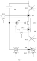
- the pixel driving circuit is a pixel driving circuit of 7T1C structure, including: a data writing path 201, a light-emitting path 202, a reset path 203, and a capacitor 204.
- An end of the data writing path 201 is connected to a data voltage, another end of the data writing path 201 is connected to a first node 205; an end of the light-emitting path 202 is connected to a positive voltage of a power supply, and another end of the light-emitting path 202 is connected to a negative voltage of the power supply;
- the reset path 203 includes a first transistor 2031 and a second transistor 2032, a first end of the first transistor 2031 being connected to a second node 206, a second end of the first transistor 2031 being connected to a reset voltage, a first end of the second transistor 2032 being connected to the first node 205, and a second end of the second transistor 2032 being connected to the second node 206; an end of the capacitor 204 is connected to the positive voltage of the power supply, and another end of the capacitor 204 is connected to the first node 205;
- the data writing path 201 is controlled by a first gating signal, the light-emitting path 202 is
- Gates of the first transistor 2031 and the second transistor 2032 are both connected to the third gating signal to control the pixel driving circuit to be in a resetting phase, a light-emitting phase, or a data writing phase, so as to achieve light emitting.
- the pixel driving circuit cyclically goes through the resetting phase, the data writing phase, and the light-emitting phase to achieve light emission.
- conduction states of the data writing path 201, the light-emitting path 202, and the reset path 203 are different, and the conduction state of the data writing path 201 is controlled by the first gating signal, the conduction state of the light-emitting path 202 is controlled by the second gating signal, and the conduction state of the reset path 203 is controlled by the third gating signal.
- the end of the data writing path 201 is connected to a data driver for receiving the data voltage.
- An end of the light-emitting path 202 is connected to a power supply voltage generator for receiving the positive voltage of the power supply.
- the other end of the light-emitting path 202 is connected to the power supply voltage generator for receiving the negative voltage of the power supply.
- the second end of the second transistor 2302 is connected to an input end of the reset voltage for receiving the reset voltage.
- the data writing path 201 may include a third transistor 2011, a fourth transistor 2012, and a fifth transistor 2013; a gate of the third transistor 2011 is connected to the first gating signal, a first end of the third transistor 2011 is connected to the data voltage, and a second end of the third transistor 2011 is connected to a third node 207; a gate of the fourth transistor 2012 is connected to the first gating signal, a first end of the fourth transistor 2012 is connected to a fourth node 208, and a second end of the fourth transistor 2012 is connected to the first node 205; a gate of the fifth transistor 2013 is connected to the first node 205, a first end of the fifth transistor 2013 is connected to the third node 207, and a second end of the fifth transistor 2013 is connected to the fourth node 208.
- the gate of the third transistor 2011 is connected to a gating signal driver to receive the first gating signal.
- the first end of the third transistor 2011 is connected to the data driver to receive the data voltage.
- the gate of the fourth transistor 2012 is connected to the gating signal driver to receive the first gating signal.
- the light-emitting path 202 may include a sixth transistor 2021, a seventh transistor 2022, a fifth transistor 2013, and a light-emitting diode 2023; a gate of the sixth transistor 2021 is connected to the second gating signal, a first end of the sixth transistor 2021 is connected to the positive voltage of the power supply, and a second end of the sixth transistor 2021 is connected to the third node 207; a gate of the seventh transistor 2022 is connected to the second gating signal, a first end of the seventh transistor 2022 is connected to the fourth node 208, and a second end of the seventh transistor 2022 is connected to the second node 206; a positive terminal of the light-emitting diode 2023 is connected to the second node 206, and a negative terminal of the light-emitting diode 2023 is connected to the negative voltage of the power supply; a gate of the fifth transistor 2013 is connected to the first node 205, a first end of the fifth transistor 2013 is
- the gate of the sixth transistor 2021 is connected to the gating signal driver to receive the second gating signal.
- the first end of the sixth transistor 2021 is connected to the power supply voltage generator to receive the positive voltage of the power supply.
- the gate of the seventh transistor 2022 is connected to the gating signal driver to receive the second gating signal.
- the negative terminal of the light-emitting diode 2023 is connected to the power supply voltage generator to receive the negative voltage of the power supply.
- three phases are cyclically generated to achieve continuous light emission.
- the three phases are the resetting phase, the data writing phase and the light-emitting phase.
- the data writing path 201 and the light-emitting path 202 are disconnected, and the reset path 203 is turned on; in response to the pixel driving circuit being in the data writing phase, the reset path 203 and the light-emitting path 202 are disconnected, and the data writing path 201 is turned on; in response to the pixel driving circuit being in the light-emitting phase, the reset path 203 and the data writing path 201 are disconnected, and the light-emitting path 202 is turned on.
- the data writing path 201 is controlled by the first gating signal
- the light-emitting path 202 is controlled by the second gating signal
- the reset path 203 is controlled by the third gating signal.
- a gating signal being at a high level
- a path controlled by the gating signal is disconnected
- the path controlled by the gating signal is turned on.
- the first gating signal controls the data writing path to be disconnected
- the second gating signal controls the light-emitting path to be disconnected
- the third gating signal controls the reset path to be turned on.
- the third gating signal controls the reset path to be disconnected, the second gating signal controls the light-emitting path to be disconnected, and the first gating signal controls the data writing path to be turned on.
- the third gating signal controls the reset path to be disconnected, the first gating signal controls the data writing path to be disconnected, and the second gating signal controls the light-emitting path to be turned on.
- the first gating signal is at a high level
- the second gating signal is at a high level
- the third gating signal is at a low level
- the reset voltage is applied to the first node 205 and the second node 206 through the reset path 203 for voltage resetting.
- the reset voltage is received through the reset path 203, and the first node 205 and the second node 206 are thereby voltage reset.
- the first gating signal is at a low level
- the second gating signal is at a high level
- the third gating signal is at a high level
- the data voltage is applied to the first node 205 through the data writing path 201 for data writing.
- the data voltage is received through the data writing path 201, and data is thereby written to the first node 205.
- the first gating signal is at a high level
- the second gating signal is at a low level
- the third gating signal is at a high level
- the positive voltage of the power supply and the data voltage written by the fifth transistor 2013 control the light-emitting diode 2023 to emit light.
- the fifth transistor 2013 is controlled by the data voltage to be turned on, and the light-emitting diode 2023 is controlled by the positive voltage of the power supply to emit light.
- each pixel of the display screen includes a pixel driving circuit.
- the display screen arranged with the pixel driving circuit at least further includes a gating signal driver and a data driver.
- the gating signal driver is connected to the gate of each transistor in the pixel driving circuit for controlling each transistor to be disconnected or turned on, and the data driving circuit is connected to the first end of the third transistor 2011 for proving the data voltage to the pixel circuit.
- the gating signal driver and the data driver may be further connected to a timing controller, and the signal output of the gating signal driver and the data driver is controlled by the timing controller.
- the display screen may further include a power supply voltage generator for providing the positive voltage of the power supply and the negative voltage of the power supply, etc. Two interfaces of the power supply voltage generator are respectively connected to one end and the other end of the light-emitting path, for sending the positive voltage to one end of the light-emitting path and the negative voltage to the other end of the light-emitting path.
- the first transistor 2031 and the second transistor 2032 are turned on, and other transistors are disconnected.
- the connected reset voltage is applied to the first node 205 and the second node 206 for voltage resetting through a path formed by the first transistor 2031 and the second transistor 2032.
- the data voltage writing phase referring to FIG. 7
- the third transistor 2011 and the fourth transistor 2012 are turned on, and other transistors are disconnected.
- the connected data voltage is applied to the first node 205 for data writing through a path formed by the third transistor 2011, the fifth transistor 2013, and the fourth transistor 2012.
- the light-emitting driving phase referring to FIG.
- the sixth transistor 2021 and the seventh transistor 2022 are turned on, and other transistors are disconnected, the light-emitting diode 2023 is turned on through a path formed by the sixth transistor 2021, the fifth transistor 2013, and the seventh transistor 2022 to complete light emission.
- the fifth transistor 2013 is a driving transistor, and the data voltage written in the data voltage writing phase is configured to drive the fifth transistor 2013 to control a conduction degree of the fifth transistor 2013, and further to control a current passing in the light-emitting driving phase, thereby controlling a light-emitting brightness of the light-emitting diode 2023.
- the third transistor 2011, the fourth transistor 2012, the sixth transistor 2021, the seventh transistor 2022, the first transistor 2031, the second transistor 2032, and the fifth transistor 2013 may be the same transistor or different transistors.
- the third transistor 2011, the fourth transistor 2012, the sixth transistor 2021, the seventh transistor 2022, the first transistor 2031, the second transistor 2032, and the fifth transistor 2013 may be at least one type of low temperature polysilicon thin film transistor, oxide semiconductor thin film transistor, or amorphous silicon thin film transistor.
- the first end of each of the third transistor 2011, the fourth transistor 2012, the sixth transistor 2021, the seventh transistor 2022, the first transistor 2031, the second transistor 2032, and the fifth transistor 2013 may be a source or a drain of the corresponding transistor; the second end of each of the third transistor 2011, the fourth transistor 2012, the sixth transistor 2021, the seventh transistor 2022, the first transistor 2031, the second transistor 2032, and the fifth transistor 2013 is a different electrode from the first end of the corresponding transistor.
- the first end is a source
- the second end is a drain
- the first end of the first transistor 2031 is a source
- the second end is a drain.
- the third transistor 2011, the fourth transistor 2012, the sixth transistor 2021, the seventh transistor 2022, the first transistor 2031, the second transistor 2032, and the fifth transistor 2013 may be single-gate transistors or dual-gate transistors, which are not specifically limited in the embodiments of the present disclosure.
- the third transistor 2011, the fourth transistor 2012, the sixth transistor 2021, the seventh transistor 2022, the first transistor 2031, the second transistor 2032, and the fifth transistor 2013 may be transistors of the same gate control type or different control types, which are not specifically limited in the embodiments of the present disclosure.
- the second transistor 2032 is a dual-gated transistor.
- the second transistor 2032 may be controlled by the same gating signal, or may be controlled by different gating signals, which is not specifically limited in the embodiments of the present disclosure.
- a disconnected dual-gated transistor is equivalent to two disconnected transistors, thereby enhancing a blocking effect when the second transistor 2032 is disconnected.
- the blocking effect of the disconnected second transistor 2032 is enhanced, which makes the leakage of the main leakage path mitigated and reduces the leakage current of the main leakage path.
- the second transistor 2032 is a dual-gate transistor
- other transistors may be each set as a single-gate transistor or a single-gate transistor, which is not specifically limited in the embodiments of the present disclosure.
- the first transistor 2031 is a single-gated transistor.
- the second transistor 2032 is set as a dual-gated transistor, such that the second transistor 2032 may effectively block the leakage of the main leakage path and reduce the second transistor 2032.
- the first transistor 2031 is set as a single-gated transistor, which reduces the space occupied by the pixel driving circuit.
- the data writing path is controlled by the first gating signal
- the light-emitting path is controlled by the second gating signal
- the reset path is controlled by the third gating signal to realize the data writing, light emitting and resetting of the pixel driving circuit, thereby completing the light-emitting process of the pixel driving circuit.
- the first end of the first transistor is connected to the second node, the second end of the first transistor is connected to the reset voltage, and the first transistor and the second transistor are controlled to be disconnected or turned on through the third gating signal, which makes the pixel driving circuit include the first transistor and the second transistor in the main leakage path, such that the leakage current during the leakage process is the current where the voltage passes through the first transistor and the second transistor, thereby reducing the leakage current of the main leakage path. In this way, the difference of the leakage current at different frequencies is reduced, thereby reducing the difficulty of fine-tuning the correction parameters.
- the working principle of the above pixel driving circuit includes the resetting phase, the data writing phase, and the light-emitting phase and will be introduced below.
- the resetting phase of the pixel driving circuit referring to FIG. 6 , the data writing path and the light-emitting path in the pixel driving circuit are disconnected, and the reset path is turned on.
- the data writing path, the light-emitting path and the reset path are controlled to be disconnected or turned on through the gating signal input from the gate of the transistor in the corresponding path.
- a high-level gating signal controls a path to be disconnected, and a low-level gating signal controls a path to be turned on.
- the gate of the third transistor, the gate of the third transistor, the gate of the fourth transistor, the gate of the sixth transistor, the gate of the seventh transistor, the gate of the first transistor, and the gate of the second transistor corresponding to the data writing path, the light-emitting path, and the reset path are connected to different gating signals, such that the transistors may be controlled independently by different gating signals, making it possible to control the transistors more precisely.
- the gate of the third transistor and the gate of the fourth transistor corresponding to the data writing path are connected to the first gating signal; the gate of the sixth transistor and the gate of the seventh transistor corresponding to the light-emitting path are connected to the second gating signal; the gate of the first transistor and the gate of the second transistor corresponding to the reset path are connected to the third gating signal.
- the first gating signal is at a high level
- the second gating signal is at a high level
- the third gating signal is at a low level.
- the pixel driving circuit forms the reset path through the first transistor and the second transistor, and the reset voltage is applied to the first node and the second node for voltage resetting through the reset path.
- the second node is connected between the second transistor and the first transistor, and is connected to the positive terminal of the light-emitting diode.
- the pixel driving circuit resets the voltage of the first node through the reset voltage, and at the same time resets the positive terminal of the light-emitting diode and resets the second node.
- the reset voltage is a negative voltage, and the magnitude of the reset voltage may be set as required.
- the reset voltage is not specifically limited.
- the reset voltage may be -3V, -5V, or -12V.
- the first node and the second node in the pixel driving circuit are voltage reset by the reset voltage, such that the data voltage written when the first node is subjected to data writing is more accurate, and the voltage of the second node is not affected by a last light-emitting phase.
- the completion of the resetting phase may be: a duration of the resetting phase reaches a first preset duration; or, the voltage of the first node reaches a first preset voltage value.
- the pixel driving circuit counts the duration of the reset process; in response to the duration of the reset process reaching the first preset duration, it is determined that the resetting of the first node is completed.
- the pixel driving circuit determines the voltage of the first node, and in response to the voltage of the first node reaching the first preset voltage value, it is determined that the resetting of the first node is completed.
- the pixel driving circuit directly controls the gating signal driver through the timing controller to complete the reset process.
- the third transistor and the fourth transistor in the pixel driving circuit are turned on, and the sixth transistor, the seventh transistor, the first transistor, and the second transistor are disconnected.
- the first gating signal is at a low level
- the second gating signal is at a high level
- the third gating signal is at a high level.
- the pixel driving circuit forms the data writing path through the third transistor, the fifth transistor and the fourth transistor, and the data voltage is applied to the first node for data writing through the data writing path.
- the data voltage may be determined according to the intensity and duration of light emission of the current pixel.
- the magnitude of the data voltage is not specifically limited.
- the data voltage may be 3V, 5V, or 12V.
- the completion of the data writing phase may be: a duration of the data writing process reaches a second preset duration; or, the voltage of the first node reaches a second preset voltage value.
- the pixel driving circuit counts the duration of the data writing process; in response to the duration of the data writing process reaching the second preset duration, it is determined that the data writing on the first node is completed.
- the pixel driving circuit determines the voltage of the first node, and in response to the voltage of the first node reaching the second preset voltage, it is determined that the data writing on the first node is completed.
- the pixel driving circuit directly controls the gating signal driver through the timing controller, and controls the pixel driving circuit to complete the data writing.
- the third transistor and the fourth transistor, the first transistor and the second transistor in the pixel driving circuit are disconnected, and the sixth transistor and the seventh transistor are turned on.
- the first gating signal is at a high level
- the second gating signal is at a low level
- the third gating signal is at a high level.
- the pixel driving circuit forms the light-emitting path through the sixth transistor, the fifth transistor, the seventh transistor and the light-emitting diode, and the positive voltage of the power supply and the data voltage written by the fifth transistor control the light-emitting diode to emit light.
- the sixth transistor and the seventh transistor are turned on by the pixel driving circuit, such that the circuit between the positive voltage of the power supply and the negative voltage of the power supply in the pixel driving circuit is turned on. In this way, a voltage between the positive and negative terminals of the light-emitting diode reaches a light-emitting voltage, thereby emitting light.
- the first node is connected to the gate of the fifth transistor.
- the fifth transistor is a driving transistor.
- the data voltage written in the data voltage writing phase is configured to drive the fifth transistor, control the conduction degree of the fifth transistor, and further control the current passing in the light-emitting driving phase, thereby controlling the light-emitting brightness of the light-emitting diode.
- I is the light-emitting current
- ⁇ and Cox are light-emitting constants
- V data is the data voltage written
- ELVDD is the positive voltage of the power supply
- W is the width of the fifth transistor
- L is the length of the fifth transistor. Therefore, ( W / L ) is an aspect ratio of the fifth transistor.
- the main leakage path provided by the embodiments of the present disclosure is the path from the first node, the second transistor, the first transistor to the reset voltage.
- the voltage that forms the leakage current in this main leakage path is the voltage difference between the first node and the reset voltage.
- the equivalent resistance in this path is the resistance of the first transistor and the second transistor that are disconnected.
- I leakage is the leakage current of the main leakage path
- V d is the voltage of the first node, that is, the driving voltage of the pixel driving circuit
- V int is the reset voltage
- R M 5 is the equivalent resistance of the first transistor
- R M 6 is the equivalent resistance of the second transistor.
- the leakage current of the main leakage path is the current formed by the equivalent resistance of the first transistor and the second transistor in series. Therefore, the leakage current is small, such that the difference in leakage current at different frequencies is small, reducing the difficulty of refining the correction parameters.
- the resetting phase, the data writing phase, and the light-emitting phase are repeatedly executed according to a light-emitting instruction to complete the image display.
- the process of disconnecting the third transistor and the fourth transistor by the pixel driving circuit may be: receiving the first gating signal of a first value through the gate of the third transistor and the gate of the fourth transistor; the first value is greater than a first voltage threshold of the third transistor and the fourth transistor, the first voltage threshold being a maximum voltage at which the third transistor and the fourth transistor can be turned on.
- the process of turning on the third transistor and the fourth transistor by the pixel driving circuit may be: the pixel driver circuit receiving the first gating signal of a second value through the gate of the third transistor and the gate of the fourth transistor; the second value is less than or equal to the first voltage threshold.
- the process of disconnecting the sixth transistor and the seventh transistor by the pixel driving circuit may be: receiving the second gating signal of a third value through the gate of the sixth transistor and the gate of the seventh transistor; the third value is greater than a second voltage threshold of the sixth transistor and the seventh transistor, the second voltage threshold being a maximum voltage value at which the sixth transistor and the seventh transistor can be turned on.
- the process of turning on the sixth transistor and the seventh transistor by the pixel driving circuit may be: the pixel driving circuit receiving the second gating signal of a fourth value through the gate of the sixth transistor and the gate of the seventh transistor; the fourth value is less than or equal to the second voltage threshold.
- the process of turning on the first transistor and the second transistor by the pixel driving circuit may be: the pixel driving circuit receiving the third gating signal of a fifth value through the gate of the first transistor and the gate of the second transistor; the fifth value is less than or equal to a third voltage threshold of the first transistor and the second transistor, the third voltage threshold being a maximum voltage value at which the sixth transistor and the seventh transistor can be turned on.
- the process of disconnecting the first transistor and the second transistor by the pixel driving circuit may be: the pixel driving circuit receiving the third gating signal of a sixth value through the gate of the first transistor and the gate of the second transistor; the sixth value is greater than the third voltage threshold.
- the first voltage threshold may be determined according to a turn-on voltage of the third transistor and a turn-on voltage of the fourth transistor
- the second voltage threshold may be determined according to a turn-on voltage of the sixth transistor and a turn-on voltage of the seventh transistor
- the third voltage threshold may be determined according to a turn-on voltage of the first transistor and a turn-on voltage of the fourth transistor.
- the first value, the third value, and the fifth value may be the same or different, which is not specifically limited in the embodiments of the present disclosure.
- the first value, the third value, and the fifth value may all be 3V or 5V.
- the values of the first gating signal, the second gating signal, and the third gating signal may refer to the values corresponding to the resetting phase in FIG. 5 .
- the first gating signal is of the first value greater than the first threshold voltage
- the second gating signal is of the third value greater than the second threshold voltage
- the third gating signal is of the fifth value less than or equal to the third threshold voltage.
- the first gating signal, the second gating signal, and the third gating signal may be generated by the gating signal driver, and the gating signal driver may be connected by the timing controller, and the timing controller controls the gating signal driver to generate the gating signal.
- the data writing path is controlled by the first gating signal
- the light-emitting path is controlled by the second gating signal
- the reset path is controlled by the third gating signal to realize the data writing, light emitting and resetting of the pixel driving circuit.
- the first end of the first transistor is connected to the second node, the second end of the first transistor is connected to the reset voltage, and the first transistor and the second transistor are controlled to be disconnected or turned on through the third gating signal, which makes the pixel driving circuit include the first transistor and the second transistor in the main leakage path, such that the leakage current during the leakage process is the current where the voltage passes through the first transistor and the second transistor, thereby reducing the leakage current of the main leakage path. In this way, the difference in the leakage current at different frequencies is reduced, thereby reducing the difficulty of fine-tuning the correction parameters.
- Embodiments of the present disclosure further provide a display screen, which includes the pixel driving circuit in the embodiments of the present disclosure.
- Embodiments of the present disclosure further provide a terminal, which includes the display screen in the embodiments of the present disclosure.
- the functions described in the embodiments of the present disclosure may be implemented by hardware, software, firmware, or any combination thereof.
- these functions may be stored in a computer-readable medium or transmitted as one or more instructions or codes on the computer-readable medium.
- the computer-readable medium includes a computer storage medium and a communication medium, where the communication medium includes any medium that facilitates the transfer of a computer program from one place to another.
- the storage medium may be any available medium that may be accessed by a general-purpose or special-purpose computer.
Landscapes
- Engineering & Computer Science (AREA)
- Physics & Mathematics (AREA)
- Computer Hardware Design (AREA)
- General Physics & Mathematics (AREA)
- Theoretical Computer Science (AREA)
- Control Of Indicators Other Than Cathode Ray Tubes (AREA)
- Control Of El Displays (AREA)
Abstract
Description
- The present application claims priority of
Chinese Patent Application No. 202010310026.1, in the title of "PIXEL DRIVING CIRCUIT, DISPLAY SCREEN, AND TERMINAL", filed on April 20, 2020 - The present disclosure relates to the field of terminal technologies, and in particular to a pixel driving circuit, a display screen, and a terminal.
- Conventionally, a light-emitting circuit includes an active-matrix organic light-emitting diode (AMOLED) panel. The AMOLED is also known as a source-matrix organic light-emitting diode or an active-matrix organic light-emitting diode, which has self-emitting properties and includes an organic material coating and a glass substrate. The AMOLED is driven by a driving current to emit light. The organic material in an organic material layer of the AMOLED emits light when a current passes through. Thin film transistor (TFT) is usually applied as the driver of AMOLED, and low temperature poly-silicon (LTPS) is a common TFT technology. Therefore, LTPS is often applied as the driver in terminal products adopting AMOLED as display screens, thereby realizing the process of displaying images.
- The present disclosure provides a pixel driving circuit, a display screen, and a terminal to reduce the difficulty of fine-tuning the correction parameters.
- In an aspect, the present disclosure provides a pixel driving circuit, including: a data writing path, a light-emitting path, a reset path and a capacitor;
- wherein an end of the data writing path is configured to receive a data voltage, another end of the data writing path is connected to a first node; an end of the light-emitting path is configured to receive a positive voltage of a power supply, and another end of the light-emitting path is configured to receive a negative voltage of the power supply;
- the reset path comprises a first transistor and a second transistor, a first end of the first transistor being connected to a second node, a second end of the first transistor being configured to receive a reset voltage, a first end of the second transistor being connected to the first node, and a second end of the second transistor being connected to the second node;
- an end of the capacitor is connected to the positive voltage of the power supply, and another end of the capacitor is connected to the first node;
- the data writing path is controlled by a first gating signal, the light-emitting path is controlled by a second gating signal, and the reset path is controlled by a third gating signal, such that the pixel driving circuit is controlled to be in a resetting phase, a light-emitting phase, or a data writing phase, for achieving light emitting.
- In another aspect, the present disclosure provides a display screen including the pixel driving circuit in the embodiments of the present disclosure.
- In a further aspect, the present disclosure provides a terminal including the display screen in the embodiments of the present disclosure.
-
-
FIG. 1 is a structural schematic view of a terminal according to an embodiment of the present disclosure. -
FIG. 2 is a structural schematic view of a pixel driving circuit according to an embodiment of the present disclosure. -
FIG. 3 is a structural schematic view of a pixel driving circuit according to another embodiment of the present disclosure. -
FIG. 4 is a structural schematic view of a pixel driving circuit according to further another embodiment of the present disclosure. -
FIG. 5 is a schematic view of a change in gating signals according to an embodiment of the present disclosure. -
FIG. 6 is a structural schematic view of a pixel driving circuit according to further another embodiment of the present disclosure. -
FIG. 7 is a structural schematic view of a pixel driving circuit according to further another embodiment of the present disclosure. -
FIG. 8 is a structural schematic view of a pixel driving circuit according to further another embodiment of the present disclosure. -
FIG. 9 is an equivalent circuit diagram of a leakage path according to an embodiment of the present disclosure. - In order to make the objectives, technical solutions, and advantages of the present disclosure clearer, the implementations of the present disclosure will be further described in detail below in conjunction with the accompanying drawings.
- The term "plurality" mentioned herein indicates two or more. The term "and/or" describes an association relationship of associated object, indicating that there may be three types of relationships. For example, A and/or B may indicate the following three cases: A alone, A and B at the same time, and B alone. The character "/" generally indicates that the associated objects before and after "/" are is in an "or" relationship.
- In the embodiments of the present disclosure, the following technical solutions are provided.
- A data writing path, a light-emitting path, a reset path and a capacitor;
- wherein an end of the data writing path is configured to receive a data voltage, another end of the data writing path is connected to a first node; an end of the light-emitting path is configured to receive a positive voltage of a power supply, and another end of the light-emitting path is configured to receive a negative voltage of the power supply;
- the reset path comprises a first transistor and a second transistor, a first end of the first transistor being connected to a second node, a second end of the first transistor being configured to receive a reset voltage, a first end of the second transistor being connected to the first node, and a second end of the second transistor being connected to the second node;
- an end of the capacitor is connected to the positive voltage of the power supply, and another end of the capacitor is connected to the first node;
- the data writing path is controlled by a first gating signal, the light-emitting path is controlled by a second gating signal, and the reset path is controlled by a third gating signal, such that the pixel driving circuit is controlled to be in a resetting phase, a light-emitting phase, or a data writing phase, for achieving light emitting.
- In some embodiments, the data writing path comprises a third transistor, a fourth transistor, and a fifth transistor;
- a gate of the third transistor is configured to receive the first gating signal, a first end of the third transistor is configured to receive the data voltage, and a second end of the third transistor is connected to a third node;
- a gate of the fourth transistor is configured to receive the first gating signal, a first end of the fourth transistor is connected to a fourth node, and a second end of the fourth transistor is connected to the first node;
- a gate of the fifth transistor is connected to the first node, a first end of the fifth transistor is connected to the third node, and a second end of the fifth transistor is connected to the fourth node.
- In other embodiments, the light-emitting path comprises a sixth transistor, a seventh transistor, a fifth transistor, and a light-emitting diode;
- a gate of the sixth transistor is configured to receive the second gating signal, a first end of the sixth transistor is configured to receive the positive voltage of the power supply, and a second end of the sixth transistor is connected to the third node;
- a gate of the seventh transistor is configured to receive the second gating signal, a first end of the seventh transistor is connected to the fourth node, and a second end of the seventh transistor is connected to the second node;
- a positive terminal of the light-emitting diode is connected to the second node, and a negative terminal of the light-emitting diode is configured to receive the negative voltage of the power supply;
- a gate of the fifth transistor is connected to the first node, a first end of the fifth transistor is connected to the third node, and a second end of the fifth transistor is connected to the fourth node.
- In other embodiments, a gate of the first transistor and a gate of the second transistor are both configured to receive the third gating signal.
- In other embodiments, in response to the pixel driving circuit being in the resetting phase, the first gating signal controls the data writing path to be disconnected, the second gating signal controls the light-emitting path to be disconnected, and the third gating signal controls the reset path to be turned on.
- In other embodiments, in response to the pixel driving circuit being in the data writing phase, the third gating signal controls the reset path to be disconnected, the second gating signal controls the light-emitting path to be disconnected, and the first gating signal controls the data writing path to be turned on.
- In other embodiments, in response to the pixel driving circuit being in the light-emitting phase, the third gating signal controls the reset path to be disconnected, the first gating signal controls the data writing path to be disconnected, and the second gating signal controls the light-emitting path to be turned on.
- In other embodiments, in the resetting phase, the first gating signal is at a high level, the second gating signal is at a high level, and the third gating signal is at a low level;
the reset voltage is received through the reset path, and the first node and the second node are voltage reset. - In other embodiments, in the data writing phase, the first gating signal is at a low level, the second gating signal is at a high level, and the third gating signal is at a high level;
the data voltage is received through the data writing path, and data is written to the first node. - In other embodiments, in the light-emitting phase, the first gating signal is at a high level, the second gating signal is at a low level, and the third gating signal is at a high level;
the fifth transistor is controlled by the data voltage to be turned on, and the light-emitting diode is controlled by the positive voltage of the power supply to emit light. - In other embodiments, the second transistor is a dual-gated transistor.
- In other embodiments, the pixel driving circuit further includes a gating signal driver;
- wherein the gating signal driver is connected to a gate of the first transistor and a gate of the second transistor;
- the gating signal driver is configured to send the third gating signal to the first transistor and the second transistor to control the first transistor and the second transistor to be disconnected or turned on.
- In other embodiments, the pixel driving circuit further includes a timing controller;
- wherein the timing controller is connected to the gating signal driver;
- the timing controller is configured to control a signal output of the gating signal driver.
- In other embodiments, the reset voltage is of any voltage value among -3V, -5V, or -12V.
- In other embodiments, during the resetting phase, data writing phase and light-emitting phase occurring cyclically, a completion of the resetting phase comprises: a duration of the resetting phase reaching a first preset duration; or, a voltage of the first node reaching a first preset voltage value.
- In other embodiments, the first transistor and the second transistor are of at least one type of: a low temperature polysilicon thin film transistor, an oxide semiconductor thin film transistor, or an amorphous silicon thin film transistor.
- In other embodiments, the pixel driving circuit further includes a power supply voltage generator;
wherein an interface of the power supply voltage generator is connected to an end of the light-emitting path, and another interface of the power supply voltage generator is connected to another end of the light-emitting path, for sending the positive voltage to the end of the light-emitting path and the negative voltage to the another end of the light-emitting path. - In other embodiments, a leakage path of the pixel drive circuit is a path including the first node, the second transistor, and the first transistor.
- The present disclosure further provides a display screen, and the display screen includes the pixel driving circuit described in the embodiments of the present disclosure.
- The present disclosure further provides a terminal, and the terminal includes the display screen described in the embodiment of the present disclosure.
- In the embodiments of the present disclosure, the data writing path is controlled by the first gating signal, the light-emitting path is controlled by the second gating signal, and the reset path is controlled by the third gating signal to realize the data writing, light emitting and resetting of the pixel driving circuit, thereby completing the light-emitting process of the pixel driving circuit, the first end of the first transistor is connected to the second node, the second end of the first transistor is connected to the reset voltage, and the first transistor and the second transistor are controlled to be disconnected or turned on through the third gating signal, which makes the pixel driving circuit include the first transistor and the second transistor in the main leakage path, such that the leakage current during the leakage process is the current where the voltage passes through the first transistor and the second transistor, thereby reducing the leakage current of the main leakage path. In this way, the difference of the leakage current at different frequencies is reduced, thereby reducing the difficulty of fine-tuning the correction parameters.
- Referring to
FIG. 1, FIG. 1 is a structural schematic view of a terminal 100 according to an embodiment of the present disclosure. The terminal 100 may be a smart phone, a tablet computer, a notebook computer, a wearable device, etc. The terminal 100 in the present disclosure may include one or more of the following components: aprocessor 110, amemory 120, and adisplay screen 130. - The
processor 110 may include one or more processing cores. Theprocessor 110 connects various parts within the terminal 100 through various interfaces and lines, for performing various functions of the terminal 100 and processing data by running or executing at least one instruction stored in thememory 120, and by calling data stored in thememory 120. In some embodiments, theprocessor 110 may be implemented with at least one of the following hardware forms: a digital signal processing (DSP), a field-programmable gate array (FPGA), a programmable logic array (PLA). Theprocessor 110 may integrate one or a combination of some of a central processing unit (CPU), a graphics processing unit (GPU), a neural-network processing unit (NPU), and a modem. The CPU mainly handles an operating system, user interface, applications, etc.; the GPU is responsible for rendering and drawing the content to be displayed on thedisplay screen 130; the NPU is configured to implement artificial intelligence (AI) functions; and the modem is configured to handle wireless communications. It can be understood that the modem may be implemented without being integrated into theprocessor 110 and through a separate chip. - The
memory 120 may include random access memory (RAM) and read-only memory (ROM). In some embodiments, thememory 120 includes a non-transitory computer-readable storage medium. Thememory 120 may be configured to store at least one instruction. Thememory 120 may include a memory program area and a memory data area. The memory program area may store instructions for implementing the operating system, instructions for at least one function (e.g., touch function, sound playback function, image playback function, etc.), instructions for implementing each of the following embodiments, etc. The memory data area may store data created according to the use of the terminal 100 (e.g., audio data, phone book), etc. - The
display screen 130 is a display component for displaying a user interface. In some embodiments, thedisplay screen 130 is a display screen with a touch function. Through the touch function, the user may use any suitable object such as a finger or a touch pen to perform a touch operation on thedisplay screen 130. - In some embodiments, the
display screen 130 includes a pixel driving circuit disclosed in the present disclosure. - The
display screen 130 is usually arranged on a front panel of the terminal 100. Thedisplay screen 130 may be designed as a full screen, a curved screen, a special-shaped screen, a double-sided screen, or a foldable screen. Thedisplay screen 130 may also be designed as a combination of a full screen and a curved screen, a combination of a special-shaped screen and a curved screen, etc., which is not limited in the embodiments. - In addition, those skilled in the art can understand that the structure of the terminal 100 shown in the attached drawing above does not constitute a limitation of the terminal 100, and the terminal 100 may include more or fewer components than shown, or a combination of certain components, or a different arrangement of components. For example, the terminal 100 further includes a microphone, a speaker, an RF circuit, an input unit, a sensor, an audio circuit, a Wireless Fidelity (Wi-Fi) module, a power supply, a Bluetooth module, and other components, which will not be described herein.
- An emerging technology, adaptive dynamic frame rate (ADFR), can effectively reduce the power consumption and delay of AMOLED. However, a TFT leakage current of a LTPS AMOLED product is large, and the degree of leakage varies at different flat rates, resulting in a large difference in leakage at different frequencies, which in turn leads to high difficulty in fine-tuning correction parameters. In order to reduce the difficulty of fine tuning of the correction parameters, the present disclosure provides a pixel driving circuit. Referring to
FIG. 2 , the present application provides a pixel driving circuit, which may be applied in an AMOLED light-emitting circuit. The pixel driving circuit is a pixel driving circuit of 7T1C structure, including: adata writing path 201, a light-emittingpath 202, areset path 203, and acapacitor 204. - An end of the
data writing path 201 is connected to a data voltage, another end of thedata writing path 201 is connected to afirst node 205; an end of the light-emittingpath 202 is connected to a positive voltage of a power supply, and another end of the light-emittingpath 202 is connected to a negative voltage of the power supply; thereset path 203 includes afirst transistor 2031 and asecond transistor 2032, a first end of thefirst transistor 2031 being connected to asecond node 206, a second end of thefirst transistor 2031 being connected to a reset voltage, a first end of thesecond transistor 2032 being connected to thefirst node 205, and a second end of thesecond transistor 2032 being connected to thesecond node 206; an end of thecapacitor 204 is connected to the positive voltage of the power supply, and another end of thecapacitor 204 is connected to thefirst node 205; thedata writing path 201 is controlled by a first gating signal, the light-emittingpath 202 is controlled by a second gating signal, and thereset path 203 is controlled by a third gating signal. Gates of thefirst transistor 2031 and thesecond transistor 2032 are both connected to the third gating signal to control the pixel driving circuit to be in a resetting phase, a light-emitting phase, or a data writing phase, so as to achieve light emitting. - The pixel driving circuit cyclically goes through the resetting phase, the data writing phase, and the light-emitting phase to achieve light emission. At different phases, conduction states of the
data writing path 201, the light-emittingpath 202, and thereset path 203 are different, and the conduction state of thedata writing path 201 is controlled by the first gating signal, the conduction state of the light-emittingpath 202 is controlled by the second gating signal, and the conduction state of thereset path 203 is controlled by the third gating signal. - The end of the
data writing path 201 is connected to a data driver for receiving the data voltage. An end of the light-emittingpath 202 is connected to a power supply voltage generator for receiving the positive voltage of the power supply. The other end of the light-emittingpath 202 is connected to the power supply voltage generator for receiving the negative voltage of the power supply. The second end of the second transistor 2302 is connected to an input end of the reset voltage for receiving the reset voltage. - In some embodiments, referring to
FIG. 3 , thedata writing path 201 may include athird transistor 2011, afourth transistor 2012, and afifth transistor 2013; a gate of thethird transistor 2011 is connected to the first gating signal, a first end of thethird transistor 2011 is connected to the data voltage, and a second end of thethird transistor 2011 is connected to athird node 207; a gate of thefourth transistor 2012 is connected to the first gating signal, a first end of thefourth transistor 2012 is connected to afourth node 208, and a second end of thefourth transistor 2012 is connected to thefirst node 205; a gate of thefifth transistor 2013 is connected to thefirst node 205, a first end of thefifth transistor 2013 is connected to thethird node 207, and a second end of thefifth transistor 2013 is connected to thefourth node 208. - The gate of the
third transistor 2011 is connected to a gating signal driver to receive the first gating signal. The first end of thethird transistor 2011 is connected to the data driver to receive the data voltage. The gate of thefourth transistor 2012 is connected to the gating signal driver to receive the first gating signal. - Referring to
FIG. 4 , the light-emittingpath 202 may include asixth transistor 2021, aseventh transistor 2022, afifth transistor 2013, and a light-emittingdiode 2023; a gate of thesixth transistor 2021 is connected to the second gating signal, a first end of thesixth transistor 2021 is connected to the positive voltage of the power supply, and a second end of thesixth transistor 2021 is connected to thethird node 207; a gate of theseventh transistor 2022 is connected to the second gating signal, a first end of theseventh transistor 2022 is connected to thefourth node 208, and a second end of theseventh transistor 2022 is connected to thesecond node 206; a positive terminal of the light-emittingdiode 2023 is connected to thesecond node 206, and a negative terminal of the light-emittingdiode 2023 is connected to the negative voltage of the power supply; a gate of thefifth transistor 2013 is connected to thefirst node 205, a first end of thefifth transistor 2013 is connected to thethird node 207, and a second end of thefifth transistor 2013 is connected to thefourth node 208. - The gate of the
sixth transistor 2021 is connected to the gating signal driver to receive the second gating signal. The first end of thesixth transistor 2021 is connected to the power supply voltage generator to receive the positive voltage of the power supply. The gate of theseventh transistor 2022 is connected to the gating signal driver to receive the second gating signal. The negative terminal of the light-emittingdiode 2023 is connected to the power supply voltage generator to receive the negative voltage of the power supply. - During a working process of the pixel driving circuit, conventionally, three phases are cyclically generated to achieve continuous light emission. The three phases are the resetting phase, the data writing phase and the light-emitting phase. In response to the pixel driving circuit being in the resetting phase, the
data writing path 201 and the light-emittingpath 202 are disconnected, and thereset path 203 is turned on; in response to the pixel driving circuit being in the data writing phase, thereset path 203 and the light-emittingpath 202 are disconnected, and thedata writing path 201 is turned on; in response to the pixel driving circuit being in the light-emitting phase, thereset path 203 and thedata writing path 201 are disconnected, and the light-emittingpath 202 is turned on. - The
data writing path 201 is controlled by the first gating signal, the light-emittingpath 202 is controlled by the second gating signal, and thereset path 203 is controlled by the third gating signal. In response to a gating signal being at a high level, a path controlled by the gating signal is disconnected, and in response to the gating signal being at a low level, the path controlled by the gating signal is turned on. In response to the pixel driving circuit being in the resetting phase, the first gating signal controls the data writing path to be disconnected, the second gating signal controls the light-emitting path to be disconnected, and the third gating signal controls the reset path to be turned on. In response to the pixel driving circuit being in the data writing phase, the third gating signal controls the reset path to be disconnected, the second gating signal controls the light-emitting path to be disconnected, and the first gating signal controls the data writing path to be turned on. In response to the pixel driving circuit being in the light-emitting phase, the third gating signal controls the reset path to be disconnected, the first gating signal controls the data writing path to be disconnected, and the second gating signal controls the light-emitting path to be turned on. - Correspondingly, referring to
FIG. 5 , in the resetting phase, the first gating signal is at a high level, the second gating signal is at a high level, and the third gating signal is at a low level; the reset voltage is applied to thefirst node 205 and thesecond node 206 through thereset path 203 for voltage resetting. The reset voltage is received through thereset path 203, and thefirst node 205 and thesecond node 206 are thereby voltage reset. In the data writing phase, the first gating signal is at a low level, the second gating signal is at a high level, and the third gating signal is at a high level; the data voltage is applied to thefirst node 205 through thedata writing path 201 for data writing. The data voltage is received through thedata writing path 201, and data is thereby written to thefirst node 205. In the light-emitting phase, the first gating signal is at a high level, the second gating signal is at a low level, and the third gating signal is at a high level; the positive voltage of the power supply and the data voltage written by thefifth transistor 2013 control the light-emittingdiode 2023 to emit light. Thefifth transistor 2013 is controlled by the data voltage to be turned on, and the light-emittingdiode 2023 is controlled by the positive voltage of the power supply to emit light. - In some embodiments, each pixel of the display screen includes a pixel driving circuit. The display screen arranged with the pixel driving circuit at least further includes a gating signal driver and a data driver. The gating signal driver is connected to the gate of each transistor in the pixel driving circuit for controlling each transistor to be disconnected or turned on, and the data driving circuit is connected to the first end of the
third transistor 2011 for proving the data voltage to the pixel circuit. In addition, the gating signal driver and the data driver may be further connected to a timing controller, and the signal output of the gating signal driver and the data driver is controlled by the timing controller. The display screen may further include a power supply voltage generator for providing the positive voltage of the power supply and the negative voltage of the power supply, etc. Two interfaces of the power supply voltage generator are respectively connected to one end and the other end of the light-emitting path, for sending the positive voltage to one end of the light-emitting path and the negative voltage to the other end of the light-emitting path. - In the resetting phase, referring to
FIG. 6 , thefirst transistor 2031 and thesecond transistor 2032 are turned on, and other transistors are disconnected. The connected reset voltage is applied to thefirst node 205 and thesecond node 206 for voltage resetting through a path formed by thefirst transistor 2031 and thesecond transistor 2032. In the data voltage writing phase, referring toFIG. 7 , thethird transistor 2011 and thefourth transistor 2012 are turned on, and other transistors are disconnected. The connected data voltage is applied to thefirst node 205 for data writing through a path formed by thethird transistor 2011, thefifth transistor 2013, and thefourth transistor 2012. In the light-emitting driving phase, referring toFIG. 8 , thesixth transistor 2021 and theseventh transistor 2022 are turned on, and other transistors are disconnected, the light-emittingdiode 2023 is turned on through a path formed by thesixth transistor 2021, thefifth transistor 2013, and theseventh transistor 2022 to complete light emission. - The
fifth transistor 2013 is a driving transistor, and the data voltage written in the data voltage writing phase is configured to drive thefifth transistor 2013 to control a conduction degree of thefifth transistor 2013, and further to control a current passing in the light-emitting driving phase, thereby controlling a light-emitting brightness of the light-emittingdiode 2023. - The
third transistor 2011, thefourth transistor 2012, thesixth transistor 2021, theseventh transistor 2022, thefirst transistor 2031, thesecond transistor 2032, and thefifth transistor 2013 may be the same transistor or different transistors. Thethird transistor 2011, thefourth transistor 2012, thesixth transistor 2021, theseventh transistor 2022, thefirst transistor 2031, thesecond transistor 2032, and thefifth transistor 2013 may be at least one type of low temperature polysilicon thin film transistor, oxide semiconductor thin film transistor, or amorphous silicon thin film transistor. - The first end of each of the
third transistor 2011, thefourth transistor 2012, thesixth transistor 2021, theseventh transistor 2022, thefirst transistor 2031, thesecond transistor 2032, and thefifth transistor 2013 may be a source or a drain of the corresponding transistor; the second end of each of thethird transistor 2011, thefourth transistor 2012, thesixth transistor 2021, theseventh transistor 2022, thefirst transistor 2031, thesecond transistor 2032, and thefifth transistor 2013 is a different electrode from the first end of the corresponding transistor. For example, when the first end is a source, the second end is a drain; when the first end is a drain, the second end is a source. In some embodiments, the first end of thefirst transistor 2031 is a source, and the second end is a drain. - In addition, the
third transistor 2011, thefourth transistor 2012, thesixth transistor 2021, theseventh transistor 2022, thefirst transistor 2031, thesecond transistor 2032, and thefifth transistor 2013 may be single-gate transistors or dual-gate transistors, which are not specifically limited in the embodiments of the present disclosure. In addition, thethird transistor 2011, thefourth transistor 2012, thesixth transistor 2021, theseventh transistor 2022, thefirst transistor 2031, thesecond transistor 2032, and thefifth transistor 2013 may be transistors of the same gate control type or different control types, which are not specifically limited in the embodiments of the present disclosure. For example, in some embodiments, thesecond transistor 2032 is a dual-gated transistor. - The
second transistor 2032 may be controlled by the same gating signal, or may be controlled by different gating signals, which is not specifically limited in the embodiments of the present disclosure. A disconnected dual-gated transistor is equivalent to two disconnected transistors, thereby enhancing a blocking effect when thesecond transistor 2032 is disconnected. - In the embodiments, by setting the
second transistor 2032 as a dual-gated transistor, the blocking effect of the disconnectedsecond transistor 2032 is enhanced, which makes the leakage of the main leakage path mitigated and reduces the leakage current of the main leakage path. - It should be noted that when the
second transistor 2032 is a dual-gate transistor, other transistors may be each set as a single-gate transistor or a single-gate transistor, which is not specifically limited in the embodiments of the present disclosure. For example, in other embodiments, thefirst transistor 2031 is a single-gated transistor. - In the embodiments, the
second transistor 2032 is set as a dual-gated transistor, such that thesecond transistor 2032 may effectively block the leakage of the main leakage path and reduce thesecond transistor 2032. Thefirst transistor 2031 is set as a single-gated transistor, which reduces the space occupied by the pixel driving circuit. - In the embodiments of the present disclosure, the data writing path is controlled by the first gating signal, the light-emitting path is controlled by the second gating signal, and the reset path is controlled by the third gating signal to realize the data writing, light emitting and resetting of the pixel driving circuit, thereby completing the light-emitting process of the pixel driving circuit. The first end of the first transistor is connected to the second node, the second end of the first transistor is connected to the reset voltage, and the first transistor and the second transistor are controlled to be disconnected or turned on through the third gating signal, which makes the pixel driving circuit include the first transistor and the second transistor in the main leakage path, such that the leakage current during the leakage process is the current where the voltage passes through the first transistor and the second transistor, thereby reducing the leakage current of the main leakage path. In this way, the difference of the leakage current at different frequencies is reduced, thereby reducing the difficulty of fine-tuning the correction parameters.
- The working principle of the above pixel driving circuit includes the resetting phase, the data writing phase, and the light-emitting phase and will be introduced below. In the resetting phase of the pixel driving circuit, referring to
FIG. 6 , the data writing path and the light-emitting path in the pixel driving circuit are disconnected, and the reset path is turned on. Among them, the data writing path, the light-emitting path and the reset path are controlled to be disconnected or turned on through the gating signal input from the gate of the transistor in the corresponding path. A high-level gating signal controls a path to be disconnected, and a low-level gating signal controls a path to be turned on. - In some embodiments, the gate of the third transistor, the gate of the third transistor, the gate of the fourth transistor, the gate of the sixth transistor, the gate of the seventh transistor, the gate of the first transistor, and the gate of the second transistor corresponding to the data writing path, the light-emitting path, and the reset path are connected to different gating signals, such that the transistors may be controlled independently by different gating signals, making it possible to control the transistors more precisely.
- In other embodiments, the gate of the third transistor and the gate of the fourth transistor corresponding to the data writing path are connected to the first gating signal; the gate of the sixth transistor and the gate of the seventh transistor corresponding to the light-emitting path are connected to the second gating signal; the gate of the first transistor and the gate of the second transistor corresponding to the reset path are connected to the third gating signal.
- Correspondingly, referring to
FIG. 5 , in the resetting phase, the first gating signal is at a high level, the second gating signal is at a high level, and the third gating signal is at a low level. - In the resetting phase, the pixel driving circuit forms the reset path through the first transistor and the second transistor, and the reset voltage is applied to the first node and the second node for voltage resetting through the reset path. Continuing to refer to
FIG. 6 , the second node is connected between the second transistor and the first transistor, and is connected to the positive terminal of the light-emitting diode. The pixel driving circuit resets the voltage of the first node through the reset voltage, and at the same time resets the positive terminal of the light-emitting diode and resets the second node. - The reset voltage is a negative voltage, and the magnitude of the reset voltage may be set as required. In the embodiments of the present disclosure, the reset voltage is not specifically limited. For example, the reset voltage may be -3V, -5V, or -12V.
- In this operation, the first node and the second node in the pixel driving circuit are voltage reset by the reset voltage, such that the data voltage written when the first node is subjected to data writing is more accurate, and the voltage of the second node is not affected by a last light-emitting phase.
- The completion of the resetting phase may be: a duration of the resetting phase reaches a first preset duration; or, the voltage of the first node reaches a first preset voltage value. Correspondingly, in some embodiments, the pixel driving circuit counts the duration of the reset process; in response to the duration of the reset process reaching the first preset duration, it is determined that the resetting of the first node is completed. In other embodiments, the pixel driving circuit determines the voltage of the first node, and in response to the voltage of the first node reaching the first preset voltage value, it is determined that the resetting of the first node is completed. In other embodiments, the pixel driving circuit directly controls the gating signal driver through the timing controller to complete the reset process.
- In the data writing phase, referring to
FIG. 7 , the third transistor and the fourth transistor in the pixel driving circuit are turned on, and the sixth transistor, the seventh transistor, the first transistor, and the second transistor are disconnected. Continuing to refer toFIG. 5 , during the data writing phase, the first gating signal is at a low level, the second gating signal is at a high level, and the third gating signal is at a high level. The pixel driving circuit forms the data writing path through the third transistor, the fifth transistor and the fourth transistor, and the data voltage is applied to the first node for data writing through the data writing path. The data voltage may be determined according to the intensity and duration of light emission of the current pixel. In the embodiments of the present disclosure, the magnitude of the data voltage is not specifically limited. For example, the data voltage may be 3V, 5V, or 12V. - The completion of the data writing phase may be: a duration of the data writing process reaches a second preset duration; or, the voltage of the first node reaches a second preset voltage value. Correspondingly, in some embodiments, the pixel driving circuit counts the duration of the data writing process; in response to the duration of the data writing process reaching the second preset duration, it is determined that the data writing on the first node is completed. In other embodiments, the pixel driving circuit determines the voltage of the first node, and in response to the voltage of the first node reaching the second preset voltage, it is determined that the data writing on the first node is completed. In other embodiments, the pixel driving circuit directly controls the gating signal driver through the timing controller, and controls the pixel driving circuit to complete the data writing.
- In the light-emitting phase, referring to
FIG. 8 , the third transistor and the fourth transistor, the first transistor and the second transistor in the pixel driving circuit are disconnected, and the sixth transistor and the seventh transistor are turned on. Continuing to refer toFIG. 5 , the first gating signal is at a high level, the second gating signal is at a low level, and the third gating signal is at a high level. The pixel driving circuit forms the light-emitting path through the sixth transistor, the fifth transistor, the seventh transistor and the light-emitting diode, and the positive voltage of the power supply and the data voltage written by the fifth transistor control the light-emitting diode to emit light. - In this phase, the sixth transistor and the seventh transistor are turned on by the pixel driving circuit, such that the circuit between the positive voltage of the power supply and the negative voltage of the power supply in the pixel driving circuit is turned on. In this way, a voltage between the positive and negative terminals of the light-emitting diode reaches a light-emitting voltage, thereby emitting light.
- The first node is connected to the gate of the fifth transistor. The fifth transistor is a driving transistor. The data voltage written in the data voltage writing phase is configured to drive the fifth transistor, control the conduction degree of the fifth transistor, and further control the current passing in the light-emitting driving phase, thereby controlling the light-emitting brightness of the light-emitting diode.
- In the light-emitting phase, a light-emitting current may be determined by Formula 1.

- Among them, I is the light-emitting current, µ and Cox are light-emitting constants, Vdata is the data voltage written, ELVDD is the positive voltage of the power supply, W is the width of the fifth transistor, and L is the length of the fifth transistor. Therefore, (W/L) is an aspect ratio of the fifth transistor.
- During the working process of the pixel driving circuit, due to the characteristics of transistors, when a transistor is disconnected, the current in the circuit cannot be completely blocked, resulting in leakage current in the pixel driving circuit. In the pixel driving circuit provided by the embodiments of the present disclosure, since the voltage difference between the first node and the reset voltage is the greatest, the main leakage path provided by the embodiments of the present disclosure is the path from the first node, the second transistor, the first transistor to the reset voltage. Continuing to refer to
FIG. 8 , the voltage that forms the leakage current in this main leakage path is the voltage difference between the first node and the reset voltage. The equivalent resistance in this path is the resistance of the first transistor and the second transistor that are disconnected. Referring toFIG. 9, FIG. 9 is an equivalent circuit diagram of the main leakage path. Therefore, the leakage current in the main leakage path may be determined by the following formula 2.

- Among them, Ileakage is the leakage current of the main leakage path, Vd is the voltage of the first node, that is, the driving voltage of the pixel driving circuit, Vint is the reset voltage, R M
5 , is the equivalent resistance of the first transistor, and R M6 is the equivalent resistance of the second transistor. - It can be seen from the above Formula 1 that in the pixel driving circuit, the leakage current of the main leakage path is the current formed by the equivalent resistance of the first transistor and the second transistor in series. Therefore, the leakage current is small, such that the difference in leakage current at different frequencies is small, reducing the difficulty of refining the correction parameters.
- It should be noted that when image display is performed on the display screen applied by the pixel driving circuit provided in the present disclosure, the resetting phase, the data writing phase, and the light-emitting phase are repeatedly executed according to a light-emitting instruction to complete the image display.
- In addition, in the embodiments of the present disclosure, the process of disconnecting the third transistor and the fourth transistor by the pixel driving circuit may be: receiving the first gating signal of a first value through the gate of the third transistor and the gate of the fourth transistor; the first value is greater than a first voltage threshold of the third transistor and the fourth transistor, the first voltage threshold being a maximum voltage at which the third transistor and the fourth transistor can be turned on. The process of turning on the third transistor and the fourth transistor by the pixel driving circuit may be: the pixel driver circuit receiving the first gating signal of a second value through the gate of the third transistor and the gate of the fourth transistor; the second value is less than or equal to the first voltage threshold.
- The process of disconnecting the sixth transistor and the seventh transistor by the pixel driving circuit may be: receiving the second gating signal of a third value through the gate of the sixth transistor and the gate of the seventh transistor; the third value is greater than a second voltage threshold of the sixth transistor and the seventh transistor, the second voltage threshold being a maximum voltage value at which the sixth transistor and the seventh transistor can be turned on. The process of turning on the sixth transistor and the seventh transistor by the pixel driving circuit may be: the pixel driving circuit receiving the second gating signal of a fourth value through the gate of the sixth transistor and the gate of the seventh transistor; the fourth value is less than or equal to the second voltage threshold.
- The process of turning on the first transistor and the second transistor by the pixel driving circuit may be: the pixel driving circuit receiving the third gating signal of a fifth value through the gate of the first transistor and the gate of the second transistor; the fifth value is less than or equal to a third voltage threshold of the first transistor and the second transistor, the third voltage threshold being a maximum voltage value at which the sixth transistor and the seventh transistor can be turned on. The process of disconnecting the first transistor and the second transistor by the pixel driving circuit may be: the pixel driving circuit receiving the third gating signal of a sixth value through the gate of the first transistor and the gate of the second transistor; the sixth value is greater than the third voltage threshold.
- The first voltage threshold may be determined according to a turn-on voltage of the third transistor and a turn-on voltage of the fourth transistor, the second voltage threshold may be determined according to a turn-on voltage of the sixth transistor and a turn-on voltage of the seventh transistor, and the third voltage threshold may be determined according to a turn-on voltage of the first transistor and a turn-on voltage of the fourth transistor. The first value, the third value, and the fifth value may be the same or different, which is not specifically limited in the embodiments of the present disclosure. For example, the first value, the third value, and the fifth value may all be 3V or 5V.
- In the operation, the values of the first gating signal, the second gating signal, and the third gating signal may refer to the values corresponding to the resetting phase in
FIG. 5 . As shown inFIG. 5 , in the resetting phase, the first gating signal is of the first value greater than the first threshold voltage, the second gating signal is of the third value greater than the second threshold voltage, and the third gating signal is of the fifth value less than or equal to the third threshold voltage. - It should be noted that the first gating signal, the second gating signal, and the third gating signal may be generated by the gating signal driver, and the gating signal driver may be connected by the timing controller, and the timing controller controls the gating signal driver to generate the gating signal.
- In the embodiments of the present disclosure, the data writing path is controlled by the first gating signal, the light-emitting path is controlled by the second gating signal, and the reset path is controlled by the third gating signal to realize the data writing, light emitting and resetting of the pixel driving circuit. In order to complete the light-emitting process of the pixel driving circuit, the first end of the first transistor is connected to the second node, the second end of the first transistor is connected to the reset voltage, and the first transistor and the second transistor are controlled to be disconnected or turned on through the third gating signal, which makes the pixel driving circuit include the first transistor and the second transistor in the main leakage path, such that the leakage current during the leakage process is the current where the voltage passes through the first transistor and the second transistor, thereby reducing the leakage current of the main leakage path. In this way, the difference in the leakage current at different frequencies is reduced, thereby reducing the difficulty of fine-tuning the correction parameters.
- Embodiments of the present disclosure further provide a display screen, which includes the pixel driving circuit in the embodiments of the present disclosure.
- Embodiments of the present disclosure further provide a terminal, which includes the display screen in the embodiments of the present disclosure.
- Those skilled in the art should be aware that, in one or more of the foregoing examples, the functions described in the embodiments of the present disclosure may be implemented by hardware, software, firmware, or any combination thereof. When implemented by software, these functions may be stored in a computer-readable medium or transmitted as one or more instructions or codes on the computer-readable medium. The computer-readable medium includes a computer storage medium and a communication medium, where the communication medium includes any medium that facilitates the transfer of a computer program from one place to another. The storage medium may be any available medium that may be accessed by a general-purpose or special-purpose computer.
- The above are only some embodiments of the present disclosure and are not intended to limit the present disclosure. Any modification, equivalent replacement, improvement, etc. made within the spirit and principle of the present disclosure shall be included within the scope of the present disclosure.
Claims (20)
- A pixel driving circuit, comprising:a data writing path, a light-emitting path, a reset path, and a capacitor;wherein an end of the data writing path is configured to receive a data voltage, another end of the data writing path is connected to a first node; an end of the light-emitting path is configured to receive a positive voltage of a power supply, and another end of the light-emitting path is configured to receive a negative voltage of the power supply;the reset path comprises a first transistor and a second transistor, a first end of the first transistor being connected to a second node, a second end of the first transistor being configured to receive a reset voltage, a first end of the second transistor being connected to the first node, and a second end of the second transistor being connected to the second node;an end of the capacitor is connected to the positive voltage of the power supply, and another end of the capacitor is connected to the first node;the data writing path is controlled by a first gating signal, the light-emitting path is controlled by a second gating signal, and the reset path is controlled by a third gating signal, such that the pixel driving circuit is controlled to be in a resetting phase, a light-emitting phase, or a data writing phase, for achieving light emitting.
- The pixel driving circuit according to claim 1, wherein the data writing path comprises a third transistor, a fourth transistor, and a fifth transistor;a gate of the third transistor is configured to receive the first gating signal, a first end of the third transistor is configured to receive the data voltage, and a second end of the third transistor is connected to a third node;a gate of the fourth transistor is configured to receive the first gating signal, a first end of the fourth transistor is connected to a fourth node, and a second end of the fourth transistor is connected to the first node;a gate of the fifth transistor is connected to the first node, a first end of the fifth transistor is connected to the third node, and a second end of the fifth transistor is connected to the fourth node.
- The pixel driving circuit according to claim 1, wherein the light-emitting path comprises a sixth transistor, a seventh transistor, a fifth transistor, and a light-emitting diode;a gate of the sixth transistor is configured to receive the second gating signal, a first end of the sixth transistor is configured to receive the positive voltage of the power supply, and a second end of the sixth transistor is connected to a third node;a gate of the seventh transistor is configured to receive the second gating signal, a first end of the seventh transistor is connected to a fourth node, and a second end of the seventh transistor is connected to the second node;a positive terminal of the light-emitting diode is connected to the second node, and a negative terminal of the light-emitting diode is configured to receive the negative voltage of the power supply;a gate of the fifth transistor is connected to the first node, a first end of the fifth transistor is connected to the third node, and a second end of the fifth transistor is connected to the fourth node.
- The pixel driving circuit according to claim 1, wherein a gate of the first transistor and a gate of the second transistor are both configured to receive the third gating signal.
- The pixel driving circuit according to claim 1, wherein in response to the pixel driving circuit being in the resetting phase, the first gating signal controls the data writing path to be disconnected, the second gating signal controls the light-emitting path to be disconnected, and the third gating signal controls the reset path to be turned on.
- The pixel driving circuit according to claim 1, wherein in response to the pixel driving circuit being in the data writing phase, the third gating signal controls the reset path to be disconnected, the second gating signal controls the light-emitting path to be disconnected, and the first gating signal controls the data writing path to be turned on.
- The pixel driving circuit according to claim 1, wherein in response to the pixel driving circuit being in the light-emitting phase, the third gating signal controls the reset path to be disconnected, the first gating signal controls the data writing path to be disconnected, and the second gating signal controls the light-emitting path to be turned on.
- The pixel driving circuit according to claim 5, wherein in the resetting phase, the first gating signal is at a high level, the second gating signal is at a high level, and the third gating signal is at a low level;
the reset voltage is received through the reset path, and the first node and the second node are voltage reset. - The pixel driving circuit according to claim 6, wherein in the data writing phase, the first gating signal is at a low level, the second gating signal is at a high level, and the third gating signal is at a high level;
the data voltage is received through the data writing path, and data is written to the first node. - The pixel driving circuit according to claim 7, wherein in the light-emitting phase, the first gating signal is at a high level, the second gating signal is at a low level, and the third gating signal is at a high level;
the fifth transistor is controlled by the data voltage to be turned on, and the light-emitting diode is controlled by the positive voltage of the power supply to emit light. - The pixel driving circuit according to claim 1, wherein the second transistor is a dual-gated transistor.
- The pixel driving circuit according to claim 1, further comprising a gating signal driver;wherein the gating signal driver is connected to a gate of the first transistor and a gate of the second transistor;the gating signal driver is configured to send the third gating signal to the first transistor and the second transistor to control the first transistor and the second transistor to be disconnected or turned on.
- The pixel driving circuit according to claim 12, further comprising a timing controller;wherein the timing controller is connected to the gating signal driver;the timing controller is configured to control a signal output of the gating signal driver.
- The pixel driving circuit according to claim 1, wherein the reset voltage is of any voltage value among -3V, -5V, or -12V.
- The pixel driving circuit according to claim 1, wherein during the resetting phase, data writing phase and light-emitting phase occurring cyclically, completion of the resetting phase comprises: a duration of the resetting phase reaching a first preset duration; or, a voltage of the first node reaching a first preset voltage value.
- The pixel driving circuit according to claim 1, wherein the first transistor and the second transistor are of at least one type of: a low temperature polysilicon thin film transistor, an oxide semiconductor thin film transistor, or an amorphous silicon thin film transistor.
- The pixel driving circuit according to claim 1, further comprising a power supply voltage generator; wherein an interface of the power supply voltage generator is connected to an end of the light-emitting path, and another interface of the power supply voltage generator is connected to another end of the light-emitting path, for sending the positive voltage to the end of the light-emitting path and the negative voltage to the another end of the light-emitting path.
- The pixel driving circuit according to claim 1, wherein a leakage path of the pixel drive circuit is a path including the first node, the second transistor, and the first transistor.
- A display screen, comprising the pixel driving circuit according to any one of claims 1-18.
- A terminal, comprising the display screen according to claim 19.
Applications Claiming Priority (2)
| Application Number | Priority Date | Filing Date | Title |
|---|---|---|---|
| CN202010310026.1A CN113539179A (en) | 2020-04-20 | 2020-04-20 | Pixel drive circuits, displays and terminals |
| PCT/CN2021/078454 WO2021213011A1 (en) | 2020-04-20 | 2021-03-01 | Pixel driving circuit, display screen, and terminal |
Publications (2)
| Publication Number | Publication Date |
|---|---|
| EP4138070A1 true EP4138070A1 (en) | 2023-02-22 |
| EP4138070A4 EP4138070A4 (en) | 2023-10-04 |
Family
ID=78123541
Family Applications (1)
| Application Number | Title | Priority Date | Filing Date |
|---|---|---|---|
| EP21793584.0A Withdrawn EP4138070A4 (en) | 2020-04-20 | 2021-03-01 | PIXEL DRIVER CIRCUIT, DISPLAY SCREEN AND TERMINAL DEVICE |
Country Status (4)
| Country | Link |
|---|---|
| US (1) | US20230063266A1 (en) |
| EP (1) | EP4138070A4 (en) |
| CN (1) | CN113539179A (en) |
| WO (1) | WO2021213011A1 (en) |
Families Citing this family (1)
| Publication number | Priority date | Publication date | Assignee | Title |
|---|---|---|---|---|
| DE112021008209T5 (en) * | 2021-09-08 | 2024-07-11 | Boe Technology Group Co., Ltd. | Pixel driving circuit and driving method therefor, display panel and display device |
Family Cites Families (24)
| Publication number | Priority date | Publication date | Assignee | Title |
|---|---|---|---|---|
| KR101152580B1 (en) * | 2010-06-30 | 2012-06-01 | 삼성모바일디스플레이주식회사 | Pixel and Organic Light Emitting Display Device Using the Same |
| KR20150070718A (en) * | 2013-12-17 | 2015-06-25 | 삼성디스플레이 주식회사 | Organic Light Emitting Display Device |
| KR102113650B1 (en) * | 2013-12-27 | 2020-06-03 | 삼성디스플레이 주식회사 | Display device and method for driving thereof |
| KR102455618B1 (en) * | 2015-02-05 | 2022-10-17 | 삼성디스플레이 주식회사 | Organic light emitting diode display |
| CN105632409B (en) * | 2016-03-23 | 2018-10-12 | 信利(惠州)智能显示有限公司 | Organic display panel image element driving method and circuit |
| US10431154B2 (en) * | 2016-06-15 | 2019-10-01 | Apple Inc. | Light-emitting diode display with reduced leakage |
| WO2018225203A1 (en) * | 2017-06-08 | 2018-12-13 | シャープ株式会社 | Display device and method for driving same |
| CN107464517A (en) * | 2017-08-17 | 2017-12-12 | 上海天马有机发光显示技术有限公司 | Driving method, drive device, display panel and the display device of display panel |
| CN107274825B (en) * | 2017-08-18 | 2020-11-24 | 上海天马微电子有限公司 | Display panel, display device, pixel driving circuit and control method thereof |
| CN107452334B (en) * | 2017-08-30 | 2020-01-03 | 京东方科技集团股份有限公司 | Pixel circuit and driving method thereof, display substrate and driving method thereof, and display device |
| KR102482575B1 (en) * | 2017-10-31 | 2022-12-28 | 엘지디스플레이 주식회사 | Organic light emitting display device |
| CN107993579B (en) * | 2017-11-29 | 2019-11-12 | 武汉天马微电子有限公司 | Display panel, driving method thereof and display device |
| KR102415275B1 (en) * | 2018-01-02 | 2022-07-01 | 삼성디스플레이 주식회사 | Pixel of organic light emitting display device and organic light emitting display device having the same |
| CN108417172B (en) * | 2018-05-14 | 2020-12-11 | 昆山国显光电有限公司 | Array substrate, display screen and display device |
| KR102600041B1 (en) * | 2018-06-07 | 2023-11-08 | 삼성디스플레이 주식회사 | Organic light emitting diode display device |
| CN110827765B (en) * | 2018-08-08 | 2021-04-09 | 京东方科技集团股份有限公司 | Display panel and driving method thereof, and display device |
| KR102811558B1 (en) * | 2018-08-17 | 2025-05-22 | 삼성디스플레이 주식회사 | Display device |
| CN109192140B (en) * | 2018-09-27 | 2020-11-24 | 武汉华星光电半导体显示技术有限公司 | Pixel driving circuit and display device |
| KR102537279B1 (en) * | 2018-09-28 | 2023-05-30 | 삼성디스플레이 주식회사 | Pixel of organic light emitting display device and organic light emitting display device having the same |
| CN109087609A (en) * | 2018-11-13 | 2018-12-25 | 京东方科技集团股份有限公司 | Pixel circuit and its driving method, display base plate, display device |
| CN109545142B (en) * | 2018-12-28 | 2020-10-20 | 上海天马微电子有限公司 | Pixel driving circuit, method, display panel and display device |
| CN110767147B (en) * | 2019-10-30 | 2022-09-09 | 武汉天马微电子有限公司 | Display method for display panel, display panel and display device |
| CN111243515A (en) * | 2020-03-19 | 2020-06-05 | 昆山国显光电有限公司 | Pixel circuit, display panel and driving method of pixel circuit |
| CN111968578B (en) * | 2020-08-31 | 2022-07-22 | 合肥维信诺科技有限公司 | Display device |
-
2020
- 2020-04-20 CN CN202010310026.1A patent/CN113539179A/en active Pending
-
2021
- 2021-03-01 WO PCT/CN2021/078454 patent/WO2021213011A1/en not_active Ceased
- 2021-03-01 EP EP21793584.0A patent/EP4138070A4/en not_active Withdrawn
-
2022
- 2022-10-20 US US18/048,250 patent/US20230063266A1/en not_active Abandoned
Also Published As
| Publication number | Publication date |
|---|---|
| WO2021213011A1 (en) | 2021-10-28 |
| CN113539179A (en) | 2021-10-22 |
| EP4138070A4 (en) | 2023-10-04 |
| US20230063266A1 (en) | 2023-03-02 |
Similar Documents
| Publication | Publication Date | Title |
|---|---|---|
| US12100342B2 (en) | Display panel and display having cascaded shift registers | |
| EP3852095B1 (en) | Pixel circuit and driving method therefor, and display device | |
| US11308841B2 (en) | Display control device, display apparatus, non-transitory recording medium, and method for controlling display control device | |
| US9704436B2 (en) | Pixel circuit, driving method thereof, array substrate, and display device | |
| US10109240B2 (en) | Displays with multiple scanning modes | |
| US10545607B2 (en) | Pixel circuit and driving method, display panel and display apparatus | |
| EP3843071A1 (en) | Pixel unit, display panel and electronic device | |
| US20160379538A1 (en) | Method and apparatus for transmitting data and display apparatus | |
| US20170193879A1 (en) | Pixel compensation circuit and method for driving the same, display panel and display device | |
| US10615244B2 (en) | OLED display panel having reset signal lines to reset pixel units and display device with the same | |
| EP3767615A1 (en) | Pixel compensation circuit, drive method, electroluminescent display panel, and display device | |
| US10885826B2 (en) | Shift register, gate driving circuit, and display device | |
| US20120293485A1 (en) | Gate signal adjustment circuit | |
| US20190206316A1 (en) | Pixel circuit and organic light emitting display device including the pixel circuit | |
| CN110930944A (en) | Display panel driving method and display device | |
| US20180190212A1 (en) | Gate scanning signal generating circuit and gate driving method | |
| US20210193070A1 (en) | Goa circuit, display panel, and electronic device | |
| EP4273849A1 (en) | Pixel circuit and driving method therefor, and display panel | |
| US20230063266A1 (en) | Pixel driving circuit, display screen, and terminal | |
| CN117935744A (en) | Display panel, driving method thereof, electronic device and storage medium | |
| US20240169889A1 (en) | Pixel driving circuit and mobile terminal | |
| WO2013027705A1 (en) | Display device, control device, and electronic apparatus | |
| CN111383598A (en) | Pixel compensation circuit and control method thereof, display driving device, and display device | |
| US11170717B2 (en) | Voltage compensation method and apparatus, and display device | |
| US9141175B2 (en) | Display device, electronic apparatus, method for controlling display device, and method for controlling electronic apparatus |
Legal Events
| Date | Code | Title | Description |
|---|---|---|---|
| STAA | Information on the status of an ep patent application or granted ep patent |
Free format text: STATUS: THE INTERNATIONAL PUBLICATION HAS BEEN MADE |
|
| PUAI | Public reference made under article 153(3) epc to a published international application that has entered the european phase |
Free format text: ORIGINAL CODE: 0009012 |
|
| STAA | Information on the status of an ep patent application or granted ep patent |
Free format text: STATUS: REQUEST FOR EXAMINATION WAS MADE |
|
| 17P | Request for examination filed |
Effective date: 20221118 |
|
| AK | Designated contracting states |
Kind code of ref document: A1 Designated state(s): AL AT BE BG CH CY CZ DE DK EE ES FI FR GB GR HR HU IE IS IT LI LT LU LV MC MK MT NL NO PL PT RO RS SE SI SK SM TR |
|
| DAV | Request for validation of the european patent (deleted) | ||
| DAX | Request for extension of the european patent (deleted) | ||
| A4 | Supplementary search report drawn up and despatched |
Effective date: 20230830 |
|
| RIC1 | Information provided on ipc code assigned before grant |
Ipc: G09G 3/3225 20160101AFI20230825BHEP |
|
| STAA | Information on the status of an ep patent application or granted ep patent |
Free format text: STATUS: THE APPLICATION IS DEEMED TO BE WITHDRAWN |
|
| 18D | Application deemed to be withdrawn |
Effective date: 20240403 |