EP4137889A1 - Procédé et appareil de mesure de métrologie - Google Patents
Procédé et appareil de mesure de métrologie Download PDFInfo
- Publication number
- EP4137889A1 EP4137889A1 EP21192381.8A EP21192381A EP4137889A1 EP 4137889 A1 EP4137889 A1 EP 4137889A1 EP 21192381 A EP21192381 A EP 21192381A EP 4137889 A1 EP4137889 A1 EP 4137889A1
- Authority
- EP
- European Patent Office
- Prior art keywords
- target
- measurement
- radiation
- tool
- metrology
- Prior art date
- Legal status (The legal status is an assumption and is not a legal conclusion. Google has not performed a legal analysis and makes no representation as to the accuracy of the status listed.)
- Withdrawn
Links
- 238000000691 measurement method Methods 0.000 title description 2
- 230000005855 radiation Effects 0.000 claims abstract description 249
- 238000005259 measurement Methods 0.000 claims abstract description 233
- 238000000034 method Methods 0.000 claims abstract description 160
- 239000000758 substrate Substances 0.000 claims abstract description 115
- 238000005286 illumination Methods 0.000 claims abstract description 67
- 230000000295 complement effect Effects 0.000 claims abstract description 22
- 238000001228 spectrum Methods 0.000 claims description 87
- 210000001747 pupil Anatomy 0.000 claims description 26
- 238000013507 mapping Methods 0.000 claims description 19
- 230000009466 transformation Effects 0.000 claims description 5
- 238000000844 transformation Methods 0.000 claims description 4
- 230000001131 transforming effect Effects 0.000 claims description 4
- 230000000877 morphologic effect Effects 0.000 claims description 3
- 239000007789 gas Substances 0.000 description 47
- 238000007689 inspection Methods 0.000 description 39
- 230000008569 process Effects 0.000 description 35
- 238000000059 patterning Methods 0.000 description 22
- 230000003287 optical effect Effects 0.000 description 21
- 230000003595 spectral effect Effects 0.000 description 20
- 210000004027 cell Anatomy 0.000 description 19
- 239000011295 pitch Substances 0.000 description 15
- 239000000047 product Substances 0.000 description 15
- 230000006870 function Effects 0.000 description 14
- 238000012545 processing Methods 0.000 description 14
- 238000013461 design Methods 0.000 description 13
- 238000001514 detection method Methods 0.000 description 13
- 238000012937 correction Methods 0.000 description 12
- 239000000463 material Substances 0.000 description 12
- 230000000737 periodic effect Effects 0.000 description 12
- 238000004519 manufacturing process Methods 0.000 description 10
- 230000007547 defect Effects 0.000 description 9
- 230000003993 interaction Effects 0.000 description 8
- 230000005670 electromagnetic radiation Effects 0.000 description 7
- 238000001459 lithography Methods 0.000 description 7
- XKRFYHLGVUSROY-UHFFFAOYSA-N Argon Chemical compound [Ar] XKRFYHLGVUSROY-UHFFFAOYSA-N 0.000 description 6
- 238000013459 approach Methods 0.000 description 6
- 230000001419 dependent effect Effects 0.000 description 6
- 238000003384 imaging method Methods 0.000 description 6
- 230000010287 polarization Effects 0.000 description 6
- 238000004458 analytical method Methods 0.000 description 5
- 238000001914 filtration Methods 0.000 description 5
- 238000013178 mathematical model Methods 0.000 description 5
- 238000005457 optimization Methods 0.000 description 5
- 230000035515 penetration Effects 0.000 description 5
- 239000004065 semiconductor Substances 0.000 description 5
- 238000000235 small-angle X-ray scattering Methods 0.000 description 5
- 238000012546 transfer Methods 0.000 description 5
- 230000009021 linear effect Effects 0.000 description 4
- 210000002381 plasma Anatomy 0.000 description 4
- 238000002310 reflectometry Methods 0.000 description 4
- 230000035945 sensitivity Effects 0.000 description 4
- 229910052717 sulfur Inorganic materials 0.000 description 4
- IJGRMHOSHXDMSA-UHFFFAOYSA-N Atomic nitrogen Chemical compound N#N IJGRMHOSHXDMSA-UHFFFAOYSA-N 0.000 description 3
- 229910052782 aluminium Inorganic materials 0.000 description 3
- XAGFODPZIPBFFR-UHFFFAOYSA-N aluminium Chemical compound [Al] XAGFODPZIPBFFR-UHFFFAOYSA-N 0.000 description 3
- 229910052786 argon Inorganic materials 0.000 description 3
- 238000004422 calculation algorithm Methods 0.000 description 3
- 238000010586 diagram Methods 0.000 description 3
- 230000000694 effects Effects 0.000 description 3
- 238000007654 immersion Methods 0.000 description 3
- 239000007788 liquid Substances 0.000 description 3
- 239000012528 membrane Substances 0.000 description 3
- 230000015654 memory Effects 0.000 description 3
- 238000000206 photolithography Methods 0.000 description 3
- 238000004626 scanning electron microscopy Methods 0.000 description 3
- 238000004088 simulation Methods 0.000 description 3
- 238000003860 storage Methods 0.000 description 3
- 230000009897 systematic effect Effects 0.000 description 3
- CURLTUGMZLYLDI-UHFFFAOYSA-N Carbon dioxide Chemical compound O=C=O CURLTUGMZLYLDI-UHFFFAOYSA-N 0.000 description 2
- QVGXLLKOCUKJST-UHFFFAOYSA-N atomic oxygen Chemical compound [O] QVGXLLKOCUKJST-UHFFFAOYSA-N 0.000 description 2
- 230000009286 beneficial effect Effects 0.000 description 2
- 230000005540 biological transmission Effects 0.000 description 2
- 238000004364 calculation method Methods 0.000 description 2
- 238000004140 cleaning Methods 0.000 description 2
- 239000002131 composite material Substances 0.000 description 2
- 238000004590 computer program Methods 0.000 description 2
- 230000003750 conditioning effect Effects 0.000 description 2
- 238000010894 electron beam technology Methods 0.000 description 2
- 238000005530 etching Methods 0.000 description 2
- 238000011156 evaluation Methods 0.000 description 2
- 238000000605 extraction Methods 0.000 description 2
- 230000004907 flux Effects 0.000 description 2
- 239000003574 free electron Substances 0.000 description 2
- 239000001307 helium Substances 0.000 description 2
- 229910052734 helium Inorganic materials 0.000 description 2
- SWQJXJOGLNCZEY-UHFFFAOYSA-N helium atom Chemical compound [He] SWQJXJOGLNCZEY-UHFFFAOYSA-N 0.000 description 2
- 238000012417 linear regression Methods 0.000 description 2
- 229910001338 liquidmetal Inorganic materials 0.000 description 2
- 239000011159 matrix material Substances 0.000 description 2
- 239000000203 mixture Substances 0.000 description 2
- 229910052754 neon Inorganic materials 0.000 description 2
- GKAOGPIIYCISHV-UHFFFAOYSA-N neon atom Chemical compound [Ne] GKAOGPIIYCISHV-UHFFFAOYSA-N 0.000 description 2
- 229910052756 noble gas Inorganic materials 0.000 description 2
- 239000001301 oxygen Substances 0.000 description 2
- 229910052760 oxygen Inorganic materials 0.000 description 2
- 239000002245 particle Substances 0.000 description 2
- 238000009304 pastoral farming Methods 0.000 description 2
- 238000004886 process control Methods 0.000 description 2
- 230000004044 response Effects 0.000 description 2
- VSZWPYCFIRKVQL-UHFFFAOYSA-N selanylidenegallium;selenium Chemical compound [Se].[Se]=[Ga].[Se]=[Ga] VSZWPYCFIRKVQL-UHFFFAOYSA-N 0.000 description 2
- 239000007787 solid Substances 0.000 description 2
- 238000013519 translation Methods 0.000 description 2
- 238000012795 verification Methods 0.000 description 2
- 229910052724 xenon Inorganic materials 0.000 description 2
- FHNFHKCVQCLJFQ-UHFFFAOYSA-N xenon atom Chemical compound [Xe] FHNFHKCVQCLJFQ-UHFFFAOYSA-N 0.000 description 2
- OKTJSMMVPCPJKN-UHFFFAOYSA-N Carbon Chemical compound [C] OKTJSMMVPCPJKN-UHFFFAOYSA-N 0.000 description 1
- VYPSYNLAJGMNEJ-UHFFFAOYSA-N Silicium dioxide Chemical compound O=[Si]=O VYPSYNLAJGMNEJ-UHFFFAOYSA-N 0.000 description 1
- XUIMIQQOPSSXEZ-UHFFFAOYSA-N Silicon Chemical group [Si] XUIMIQQOPSSXEZ-UHFFFAOYSA-N 0.000 description 1
- 238000000333 X-ray scattering Methods 0.000 description 1
- QCWXUUIWCKQGHC-UHFFFAOYSA-N Zirconium Chemical compound [Zr] QCWXUUIWCKQGHC-UHFFFAOYSA-N 0.000 description 1
- 238000000137 annealing Methods 0.000 description 1
- 238000000429 assembly Methods 0.000 description 1
- 230000000712 assembly Effects 0.000 description 1
- 239000006227 byproduct Substances 0.000 description 1
- 229910052799 carbon Inorganic materials 0.000 description 1
- 229910002092 carbon dioxide Inorganic materials 0.000 description 1
- 239000001569 carbon dioxide Substances 0.000 description 1
- 229910052729 chemical element Inorganic materials 0.000 description 1
- 230000001427 coherent effect Effects 0.000 description 1
- 238000004040 coloring Methods 0.000 description 1
- 238000011109 contamination Methods 0.000 description 1
- 230000008878 coupling Effects 0.000 description 1
- 238000010168 coupling process Methods 0.000 description 1
- 238000005859 coupling reaction Methods 0.000 description 1
- 230000003247 decreasing effect Effects 0.000 description 1
- 238000009826 distribution Methods 0.000 description 1
- 230000009977 dual effect Effects 0.000 description 1
- 238000005516 engineering process Methods 0.000 description 1
- 238000001900 extreme ultraviolet lithography Methods 0.000 description 1
- 239000000835 fiber Substances 0.000 description 1
- 239000010408 film Substances 0.000 description 1
- 239000005350 fused silica glass Substances 0.000 description 1
- 238000000671 immersion lithography Methods 0.000 description 1
- 230000002452 interceptive effect Effects 0.000 description 1
- 229910052743 krypton Inorganic materials 0.000 description 1
- DNNSSWSSYDEUBZ-UHFFFAOYSA-N krypton atom Chemical compound [Kr] DNNSSWSSYDEUBZ-UHFFFAOYSA-N 0.000 description 1
- 230000000670 limiting effect Effects 0.000 description 1
- 238000012886 linear function Methods 0.000 description 1
- 239000004973 liquid crystal related substance Substances 0.000 description 1
- 238000011068 loading method Methods 0.000 description 1
- 238000010801 machine learning Methods 0.000 description 1
- 230000005381 magnetic domain Effects 0.000 description 1
- 229910052751 metal Inorganic materials 0.000 description 1
- 239000002184 metal Substances 0.000 description 1
- 230000003278 mimic effect Effects 0.000 description 1
- 238000012986 modification Methods 0.000 description 1
- 230000004048 modification Effects 0.000 description 1
- 229910052757 nitrogen Inorganic materials 0.000 description 1
- 230000009022 nonlinear effect Effects 0.000 description 1
- 230000003647 oxidation Effects 0.000 description 1
- 238000007254 oxidation reaction Methods 0.000 description 1
- 238000007781 pre-processing Methods 0.000 description 1
- 238000002360 preparation method Methods 0.000 description 1
- 230000002829 reductive effect Effects 0.000 description 1
- 238000000985 reflectance spectrum Methods 0.000 description 1
- 238000007493 shaping process Methods 0.000 description 1
- 239000002904 solvent Substances 0.000 description 1
- 238000012306 spectroscopic technique Methods 0.000 description 1
- 230000003068 static effect Effects 0.000 description 1
- 238000012916 structural analysis Methods 0.000 description 1
- 239000000126 substance Substances 0.000 description 1
- 239000010409 thin film Substances 0.000 description 1
- XLYOFNOQVPJJNP-UHFFFAOYSA-N water Substances O XLYOFNOQVPJJNP-UHFFFAOYSA-N 0.000 description 1
- 229910052726 zirconium Inorganic materials 0.000 description 1
Images


Classifications
-
- G—PHYSICS
- G03—PHOTOGRAPHY; CINEMATOGRAPHY; ANALOGOUS TECHNIQUES USING WAVES OTHER THAN OPTICAL WAVES; ELECTROGRAPHY; HOLOGRAPHY
- G03F—PHOTOMECHANICAL PRODUCTION OF TEXTURED OR PATTERNED SURFACES, e.g. FOR PRINTING, FOR PROCESSING OF SEMICONDUCTOR DEVICES; MATERIALS THEREFOR; ORIGINALS THEREFOR; APPARATUS SPECIALLY ADAPTED THEREFOR
- G03F7/00—Photomechanical, e.g. photolithographic, production of textured or patterned surfaces, e.g. printing surfaces; Materials therefor, e.g. comprising photoresists; Apparatus specially adapted therefor
- G03F7/70—Microphotolithographic exposure; Apparatus therefor
- G03F7/70483—Information management; Active and passive control; Testing; Wafer monitoring, e.g. pattern monitoring
- G03F7/70605—Workpiece metrology
- G03F7/70616—Monitoring the printed patterns
Definitions
- the present invention relates to methods and apparatus for use in measuring parameters of a structure fabricated in or on a substrate. Specific arrangements may relate to, but need not be limited to, measurement of overlay or side wall angle.
- a lithographic apparatus is a machine constructed to apply a desired pattern onto a substrate.
- a lithographic apparatus can be used, for example, in the manufacture of integrated circuits (ICs).
- a lithographic apparatus may, for example, project a pattern (also often referred to as "design layout" or "design") at a patterning device (e.g., a mask) onto a layer of radiation-sensitive material (resist) provided on a substrate (e.g., a wafer).
- a lithographic apparatus may use electromagnetic radiation.
- the wavelength of this radiation determines the minimum size of features which can be formed on the substrate. Typical wavelengths currently in use are 365 nm (i-line), 248 nm, 193 nm and 13.5 nm.
- a lithographic apparatus which uses extreme ultraviolet (EUV) radiation, having a wavelength within the range 4-20 nm, for example 6.7 nm or 13.5 nm, may be used to form smaller features on a substrate than a lithographic apparatus which uses, for example, radiation with a wavelength of 193 nm.
- EUV extreme ultraviolet
- Low-ki lithography may be used to process features with dimensions smaller than the classical resolution limit of a lithographic apparatus.
- ⁇ the wavelength of radiation employed
- NA the numerical aperture of the projection optics in the lithographic apparatus
- CD is the "critical dimension" (generally the smallest feature size printed, but in this case half-pitch)
- ki is an empirical resolution factor.
- sophisticated fine-tuning steps may be applied to the lithographic projection apparatus and/or design layout.
- RET resolution enhancement techniques
- a method may require a target in the form of a simple grating that is large enough that a measurement beam generates a spot that is smaller than the grating (i.e., the grating is underfilled).
- properties of the grating can be calculated by simulating interaction of scattered radiation with a mathematical model of the target structure. Parameters of the model are adjusted until the simulated interaction produces a diffraction pattern similar to that observed from the real target.
- diffraction-based overlay can be measured using such apparatus, as described in published patent application US2006066855A1 .
- Diffraction-based overlay metrology using dark-field imaging of the diffraction orders enables overlay measurements on smaller targets. These targets can be smaller than the illumination spot and may be surrounded by product structures on a wafer. Examples of dark field imaging metrology can be found in numerous published patent applications, such as for example US2011102753A1 and US20120044470A . Multiple gratings can be measured in one image, using a composite grating target.
- the known scatterometers tend to use light in the visible or near-infrared (IR) wave range, which requires the pitch of the grating to be much coarser than the actual product structures whose properties are actually of interest.
- Such product features may be defined using deep ultraviolet (DUV), extreme ultraviolet (EUV) or X-ray radiation having far shorter wavelengths. Unfortunately, such wavelengths are not normally available or usable for metrology.
- the dimensions of modern product structures are so small that they cannot be imaged by optical metrology techniques.
- Small features include for example those formed by multiple patterning processes, and/or pitch-multiplication.
- targets used for high-volume metrology often use features that are much larger than the products whose overlay errors or critical dimensions are the property of interest.
- the measurement results are only indirectly related to the dimensions of the real product structures, and may be inaccurate because the metrology target does not suffer the same distortions under optical projection in the lithographic apparatus, and/or different processing in other steps of the manufacturing process.
- SEM scanning electron microscopy
- electrons are not able to penetrate through thick process layers, which makes them less suitable for metrology applications.
- Other techniques such as measuring electrical properties using contact pads is also known, but it provides only indirect evidence of the true product structure.
- One such method of generating suitably high frequency radiation may be using a pump radiation, or called a drive radiation (e.g., infrared IR radiation) to excite a generating medium, thereby generating an emitted radiation, optionally a high harmonic generation comprising high frequency radiation.
- a pump radiation or called a drive radiation (e.g., infrared IR radiation) to excite a generating medium, thereby generating an emitted radiation, optionally a high harmonic generation comprising high frequency radiation.
- a drive radiation e.g., infrared IR radiation
- overlay metrology can be performed by illuminating, using electromagnetic radiation, an overlay target or other structure and measuring radiation diffracted or reflected from the overlay target.
- the target may comprise two gratings on top of each other.
- Asymmetry in the diffracted radiation is defined as the difference between an intensity of the negative and corresponding positive diffraction orders, for example the difference between the -1 st and +1 st diffraction orders. This asymmetry is dependent on the lateral shift (the overlay shift) between the top and bottom grating of the overlay target. The asymmetry of an overlay grating thus allows evaluation of overlay.
- the term "intensity” encompasses incident power (in watts) of radiation, which may be SXR radiation, per unit area.
- the area may be detector or sensor area.
- the term “signal” encompasses an electrical charge collected by a detector (or sensor) pixel during an exposure. The signal may be expressed in coulombs or in analog-digital units (ADU). The signal is proportional to irradiance and exposure time (the proportionality constant is wavelength dependent).
- the term “reflectance” encompasses the ratio of diffracted spectral flux to spectral flux incident upon a target. The reflectance may depend on the target properties, target orientation, the wavelength, and/or the diffraction order number. The reflectance of a target may vary (drift) over time. Reflectance may be measured as an average over an exposure time.
- Such evaluation typically requires calibration of the relation between asymmetry and overlay (in other words, the extraction of the sensitivity of overlay to asymmetry). This can be done using measurements on multiple overlay targets with known overlay shifts (overlay biases).
- One exemplary calibration method uses measurements on two overlay targets with different overlay shift to extract overlay (and the sensitivity).
- system or tool asymmetries
- a single measurement of the diffracted radiation from a target suffices for overlay extraction.
- System asymmetry e.g. a different gain of the detector for the -1 st order compared to the 1 st order
- To remove this tool-induced asymmetry a second measurement on the same target is done after the target has been rotated in-plane by 180 degrees. The first measurement is referred to as the nominal target orientation measurement, the second one as the rotated target orientation measurement.
- the rotated measurement results in diffracted radiation from the target that is also rotated.
- a tool-induced asymmetry will not be rotated.
- the combination of nominal and rotated measurement allows distinction of overlay asymmetry from system asymmetry.
- a method of measuring a target on a substrate using a metrology tool comprising an illumination source operable to emit an illumination beam for illuminating the target and a metrology sensor for collecting the scattered radiation having been scattered by the target, the surface of said substrate defining a substrate plane extending over a first tool direction and a second tool direction orthogonal to said first tool direction, where the first tool direction, second tool direction and a third tool direction orthogonal said first tool direction and second tool direction together defines a tool coordinate system
- the method comprising: performing at least one pair of measurement acquisitions, said at least one pair of measurement acquisitions comprising a first measurement acquisition of the target at a first target orientation with respect to the illumination beam; and a second measurement acquisition of the target at a second target orientation with respect to the illumination beam, wherein said first target orientation is defined by a target angle between a target coordinate system and said tool coordinate system around an axis perpendicular to the substrate plane, wherein said target angle for at least one of said at least one
- the terms "radiation” and “beam” are used to encompass all types of electromagnetic radiation and particle radiation, including ultraviolet radiation (e.g. with a wavelength of 365, 248, 193, 157 or 126 nm), EUV (extreme ultra-violet radiation, e.g. having a wavelength in the range of about 5-100 nm), X-ray radiation, electron beam radiation and other particle radiation.
- ultraviolet radiation e.g. with a wavelength of 365, 248, 193, 157 or 126 nm
- EUV extreme ultra-violet radiation, e.g. having a wavelength in the range of about 5-100 nm
- X-ray radiation e.g. having a wavelength in the range of about 5-100 nm
- electron beam radiation e.g. having a wavelength in the range of about 5-100 nm
- reticle may be broadly interpreted as referring to a generic patterning device that can be used to endow an incoming radiation beam with a patterned cross-section, corresponding to a pattern that is to be created in a target portion of the substrate.
- the term “light valve” can also be used in this context.
- examples of other such patterning devices include a programmable mirror array and a programmable LCD array.
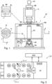
- FIG. 1 schematically depicts a lithographic apparatus LA.
- the lithographic apparatus LA includes an illumination system (also referred to as illuminator) IL configured to condition a radiation beam B (e.g., UV radiation, DUV radiation, EUV radiation or X-ray radiation), a mask support (e.g., a mask table) T constructed to support a patterning device (e.g., a mask) MA and connected to a first positioner PM configured to accurately position the patterning device MA in accordance with certain parameters, a substrate support (e.g., a wafer table) WT constructed to hold a substrate (e.g., a resist coated wafer) W and connected to a second positioner PW configured to accurately position the substrate support in accordance with certain parameters, and a projection system (e.g., a refractive projection lens system) PS configured to project a pattern imparted to the radiation beam B by patterning device MA onto a target portion C (e.g., comprising one or more dies)
- the illumination system IL receives a radiation beam from a radiation source SO, e.g. via a beam delivery system BD.
- the illumination system IL may include various types of optical components, such as refractive, reflective, diffractive, magnetic, electromagnetic, electrostatic, and/or other types of optical components, or any combination thereof, for directing, shaping, and/or controlling radiation.
- the illuminator IL may be used to condition the radiation beam B to have a desired spatial and angular intensity distribution in its cross section at a plane of the patterning device MA.
- projection system PS used herein should be broadly interpreted as encompassing various types of projection system, including refractive, reflective, diffractive, catadioptric, anamorphic, magnetic, electromagnetic and/or electrostatic optical systems, or any combination thereof, as appropriate for the exposure radiation being used, and/or for other factors such as the use of an immersion liquid or the use of a vacuum. Any use of the term “projection lens” herein may be considered as synonymous with the more general term “projection system” PS.
- the lithographic apparatus LA may be of a type wherein at least a portion of the substrate may be covered by a liquid having a relatively high refractive index, e.g., water, so as to fill a space between the projection system PS and the substrate W - which is also referred to as immersion lithography. More information on immersion techniques is given in US6952253 , which is incorporated herein by reference in its entirety.
- a liquid having a relatively high refractive index e.g., water
- the lithographic apparatus LA may also be of a type having two or more substrate supports WT (also named “dual stage”).
- the substrate supports WT may be used in parallel, and/or steps in preparation of a subsequent exposure of the substrate W may be carried out on the substrate W located on one of the substrate support WT while another substrate W on the other substrate support WT is being used for exposing a pattern on the other substrate W.
- the lithographic apparatus LA may comprise a measurement stage.
- the measurement stage is arranged to hold a sensor and/or a cleaning device.
- the sensor may be arranged to measure a property of the projection system PS or a property of the radiation beam B.
- the measurement stage may hold multiple sensors.
- the cleaning device may be arranged to clean part of the lithographic apparatus, for example a part of the projection system PS or a part of a system that provides the immersion liquid.
- the measurement stage may move beneath the projection system PS when the substrate support WT is away from the projection system PS.
- the radiation beam B is incident on the patterning device, e.g. mask, MA which is held on the mask support T, and is patterned by the pattern (design layout) present on patterning device MA. Having traversed the mask MA, the radiation beam B passes through the projection system PS, which focuses the beam onto a target portion C of the substrate W. With the aid of the second positioner PW and a position measurement system IF, the substrate support WT may be moved accurately, e.g., so as to position different target portions C in the path of the radiation beam B at a focused and aligned position.
- the patterning device e.g. mask, MA which is held on the mask support T
- the pattern (design layout) present on patterning device MA Having traversed the mask MA, the radiation beam B passes through the projection system PS, which focuses the beam onto a target portion C of the substrate W.
- the substrate support WT may be moved accurately, e.g., so as to position different target portions C in the path of the radiation beam B at a focused
- first positioner PM and possibly another position sensor may be used to accurately position the patterning device MA with respect to the path of the radiation beam B.
- Patterning device MA and substrate W may be aligned using mask alignment marks M1, M2 and substrate alignment marks PI, P2.
- substrate alignment marks PI, P2 as illustrated occupy dedicated target portions, they may be located in spaces between target portions.
- Substrate alignment marks PI, P2 are known as scribe-lane alignment marks when these are located between the target portions C.
- the lithographic apparatus LA may form part of a lithographic cell LC, also sometimes referred to as a lithocell or (litho)cluster, which often also includes apparatus to perform pre- and post-exposure processes on a substrate W.
- a lithographic cell LC also sometimes referred to as a lithocell or (litho)cluster
- these include spin coaters SC to deposit resist layers, developers DE to develop exposed resist, chill plates CH and bake plates BK, e.g. for conditioning the temperature of substrates W e.g. for conditioning solvents in the resist layers.
- a substrate handler, or robot, RO picks up substrates W from input/output ports I/O1, I/O2, moves them between the different process apparatus and delivers the substrates W to the loading bay LB of the lithographic apparatus LA.
- the devices in the lithocell may be under the control of a track control unit TCU that in itself may be controlled by a supervisory control system SCS, which may also control the lithographic apparatus LA, e.g. via lithography control unit LACU.
- a supervisory control system SCS which may also control the lithographic apparatus LA, e.g. via lithography control unit LACU.
- Metrology tools MT In lithographic processes, it is desirable to make frequently measurements of the structures created, e.g., for process control and verification. Tools to make such measurement may be called metrology tools MT.
- Different types of metrology tools MT for making such measurements are known, including scanning electron microscopes or various forms of scatterometer metrology tools MT.
- Scatterometers are versatile instruments which allow measurements of the parameters of a lithographic process by having a metrology sensor in or close to the pupil or a conjugate plane with the pupil of the objective of the scatterometer, measurements usually referred as pupil based measurements, or by having the sensor in or close to an image plane or a plane conjugate with the image plane, in which case the measurements are usually referred as image or field based measurements.
- Aforementioned scatterometers may measure gratings using light from hard X-ray (HXR), soft X-ray (SXR), extreme ultraviolet (EUV), visible to near-infrared (IR) and IR wavelength range.
- HXR hard X-ray
- SXR soft X-ray
- EUV extreme ultraviolet
- IR near-infrared
- the aforementioned scatterometers may optionally be a small-angle X-ray scattering metrology tool.
- inspection tools and/or metrology tools may be included in the lithocell LC. If errors are detected, adjustments, for example, may be made to exposures of subsequent substrates or to other processing steps that are to be performed on the substrates W, especially if the inspection is done before other substrates W of the same batch or lot are still to be exposed or processed.
- An inspection apparatus which may also be referred to as a metrology apparatus, is used to determine properties of the substrates W, and in particular, how properties of different substrates W vary or how properties associated with different layers of the same substrate W vary from layer to layer.
- the inspection apparatus may alternatively be constructed to identify defects on the substrate W and may, for example, be part of the lithocell LC, or may be integrated into the lithographic apparatus LA, or may even be a stand-alone device.
- the inspection apparatus may measure the properties on a latent image (image in a resist layer after the exposure), or on a semi-latent image (image in a resist layer after a post-exposure bake step PEB), or on a developed resist image (in which the exposed or unexposed parts of the resist have been removed), or even on an etched image (after a pattern transfer step such as etching).
- the scatterometer MT is an angular resolved scatterometer.
- reconstruction methods may be applied to the measured signal to reconstruct or calculate properties of the grating.
- Such reconstruction may, for example, result from simulating interaction of scattered radiation with a mathematical model of the target structure and comparing the simulation results with those of a measurement. Parameters of the mathematical model are adjusted until the simulated interaction produces a diffraction pattern similar to that observed from the real target.
- the scatterometer MT is a spectroscopic scatterometer MT.
- the radiation emitted by a radiation source is directed onto the target and the reflected, transmitted or scattered radiation from the target is directed to a spectrometer detector, which measures a spectrum (i.e. a measurement of intensity as a function of wavelength) of the specular reflected radiation. From this data, the structure or profile of the target giving rise to the detected spectrum may be reconstructed, e.g. by Rigorous Coupled Wave Analysis and non-linear regression or by comparison with a library of simulated spectra.
- the scatterometer MT is an ellipsometric scatterometer.
- the ellipsometric scatterometer allows for determining parameters of a lithographic process by measuring scattered or transmitted radiation for each polarization states.
- Such metrology apparatus emits polarized light (such as linear, circular, or elliptic) by using, for example, appropriate polarization filters in the illumination section of the metrology apparatus.
- a source suitable for the metrology apparatus may provide polarized radiation as well.
- the scatterometer MT is adapted to measure the overlay of two misaligned gratings or periodic structures by measuring asymmetry in the reflected spectrum and/or the detection configuration, the asymmetry being related to the extent of the overlay.
- the two (maybe overlapping) grating structures may be applied in two different layers (not necessarily consecutive layers), and may be formed substantially at the same position on the wafer.
- the scatterometer may have a symmetrical detection configuration as described e.g. in co-owned patent application EP1,628,164A , such that any asymmetry is clearly distinguishable. This provides a straightforward way to measure misalignment in gratings.
- Focus and dose may be determined simultaneously by scatterometry (or alternatively by scanning electron microscopy) as described in US patent application US2011-0249244 , incorporated herein by reference in its entirety.
- a single structure may be used which has a unique combination of critical dimension and sidewall angle measurements for each point in a focus energy matrix (FEM - also referred to as Focus Exposure Matrix). If these unique combinations of critical dimension and sidewall angle are available, the focus and dose values may be uniquely determined from these measurements.
- FEM focus energy matrix
- a metrology target may be an ensemble of composite gratings, formed by a lithographic process, mostly in resist, but also after etch process for example.
- the pitch and line-width of the structures in the gratings may strongly depend on the measurement optics (in particular the NA of the optics) to be able to capture diffraction orders coming from the metrology targets.
- the diffracted signal may be used to determine shifts between two layers (also referred to 'overlay') or may be used to reconstruct at least part of the original grating as produced by the lithographic process. This reconstruction may be used to provide guidance of the quality of the lithographic process and may be used to control at least part of the lithographic process.
- Targets may have smaller sub-segmentation which are configured to mimic dimensions of the functional part of the design layout in a target. Due to this sub-segmentation, the targets will behave more similar to the functional part of the design layout such that the overall process parameter measurements resemble the functional part of the design layout better.
- the targets may be measured in an underfilled mode or in an overfilled mode. In the underfilled mode, the measurement beam generates a spot that is smaller than the overall target. In the overfilled mode, the measurement beam generates a spot that is larger than the overall target. In such overfilled mode, it may also be possible to measure different targets simultaneously, thus determining different processing parameters at the same time.
- substrate measurement recipe may include one or more parameters of the measurement itself, one or more parameters of the one or more patterns measured, or both.
- the measurement used in a substrate measurement recipe is a diffraction-based optical measurement
- one or more of the parameters of the measurement may include the wavelength of the radiation, the polarization of the radiation, the incident angle of radiation relative to the substrate, the orientation of radiation relative to a pattern on the substrate, etc.
- One of the criteria to select a measurement recipe may, for example, be a sensitivity of one of the measurement parameters to processing variations. More examples are described in US patent application US2016-0161863 and published US patent application US 2016/0370717A1 incorporated herein by reference in its entirety.
- the patterning process in a lithographic apparatus LA may be one of the most critical steps in the processing which requires high accuracy of dimensioning and placement of structures on the substrate W.
- three systems may be combined in a so called “holistic" control environment as schematically depicted in Fig. 3 .
- One of these systems is the lithographic apparatus LA which is (virtually) connected to a metrology tool MT (a second system) and to a computer system CL (a third system).
- the key of such "holistic" environment is to optimize the cooperation between these three systems to enhance the overall process window and provide tight control loops to ensure that the patterning performed by the lithographic apparatus LA stays within a process window.
- the process window defines a range of process parameters (e.g. dose, focus, overlay) within which a specific manufacturing process yields a defined result (e.g. a functional semiconductor device) - maybe within which the process parameters in the lithographic process or patterning process are allowed to vary.
- the computer system CL may use (part of) the design layout to be patterned to predict which resolution enhancement techniques to use and to perform computational lithography simulations and calculations to determine which mask layout and lithographic apparatus settings achieve the largest overall process window of the patterning process (depicted in Fig. 3 by the double arrow in the first scale SC1).
- the resolution enhancement techniques may be arranged to match the patterning possibilities of the lithographic apparatus LA.
- the computer system CL may also be used to detect where within the process window the lithographic apparatus LA is currently operating (e.g. using input from the metrology tool MET) to predict whether defects may be present due to e.g. sub-optimal processing (depicted in Fig. 3 by the arrow pointing "0" in the second scale SC2).
- the metrology tool MT may provide input to the computer system CL to enable accurate simulations and predictions, and may provide feedback to the lithographic apparatus LA to identify possible drifts, e.g. in a calibration status of the lithographic apparatus LA (depicted in Fig. 3 by the multiple arrows in the third scale SC3).
- Metrology tools MT may use electromagnetic radiation to interrogate a structure. Properties of the radiation (e.g. wavelength, bandwidth, power) can affect different measurement characteristics of the tool, with shorter wavelengths generally allowing for increased resolution. Radiation wavelength has an effect on the resolution the metrology tool can achieve. Therefore, in order to be able to measure structures with features having small dimensions, metrology tools MT with short wavelength radiation sources are preferred.
- electromagnetic radiation e.g. wavelength, bandwidth, power
- radiation wavelength can affect measurement characteristics
- penetration depth and the transparency/opacity of materials to be inspected at the radiation wavelength.
- radiation can be used for measurements in transmission or reflection.
- the type of measurement can affect whether information is obtained about the surface and/or the bulk interior of a structure/substrate. Therefore, penetration depth and opacity are another element to be taken into account when selecting radiation wavelength for a metrology tool.
- metrology tools MT with short wavelengths are preferred. This may include wavelengths shorter than visible wavelengths, for example in the UV, EUV, and X-ray portions of the electromagnetic spectrum.
- Hard X-ray methods such as Transmitted Small Angle X-ray Scattering (TSAXS) make use of the high resolution and high penetration depth of hard X-rays and may therefore operate in transmission.
- Soft X-rays and EUV do not penetrate the target as far but may induce a rich optical response in the material to be probed. This may be due the optical properties of many semiconductor materials, and due to the structures being comparable in size to the probing wavelength.
- EUV and/or soft X-ray metrology tools MT may operate in reflection, for example by imaging, or by analysing diffraction patterns from, a lithographically patterned structure.
- HVM high volume manufacturing
- applications in high volume manufacturing (HVM) applications may be limited due to a lack of available high-brilliance radiation sources at the required wavelengths.
- HVM high volume manufacturing
- commonly used sources in industrial applications include X-ray tubes.
- X-ray tubes including advanced X-ray tubes for example based on liquid metal anodes or rotating anodes, may be relatively affordable and compact, but may lack brilliance required for HVM applications.
- High brilliance X-ray sources such as Synchrotron Light Sources (SLSs) and X-ray Free Electron Lasers (XFELs) currently exist, but their size (>100m) and high cost (multi-100-million euro), makes them prohibitively large and expensive for metrology applications. Similarly, there is a lack of availability of sufficiently bright EUV and soft X-ray radiation sources.
- SLSs Synchrotron Light Sources
- XFELs X-ray Free Electron Lasers
- FIG. 4 One example of a metrology apparatus, such as a scatterometer, is depicted in Figure 4 . It may comprise a broadband (e.g. white light) radiation projector 2 which projects radiation 5 onto a substrate W. The reflected or scattered radiation 10 is passed to a spectrometer detector 4, which measures a spectrum 6 (i.e. a measurement of intensity I as a function of wavelength ⁇ ) of the specular reflected radiation. From this data, the structure or profile 8 giving rise to the detected spectrum may be reconstructed by processing unit PU, e.g. by Rigorous Coupled Wave Analysis and non-linear regression or by comparison with a library of simulated spectra as shown at the bottom of Figure 4 .
- a broadband radiation projector 2 which projects radiation 5 onto a substrate W.
- the reflected or scattered radiation 10 is passed to a spectrometer detector 4, which measures a spectrum 6 (i.e. a measurement of intensity I as a function of wavelength ⁇ ) of the specular reflected radiation. From this data, the
- a scatterometer may be configured as a normal-incidence scatterometer or an oblique-incidence scatterometer.
- a transmissive version of the example of a metrology apparatus such as a scatterometer shown in Figure 4 , is depicted in Figure 5 .
- the transmitted radiation 11 is passed to a spectrometer detector 4, which measures a spectrum 6 as discussed for Figure 4 .
- a scatterometer may be configured as a normal-incidence scatterometer or an oblique-incidence scatterometer.
- the transmissive version using hard X-ray radiation with wavelength ⁇ 1 nm, optionally ⁇ 0.1 nm, optionally ⁇ 0.01 nm.
- optical metrology methods it has also been considered to use hard X-ray, soft X-rays or EUV radiation, for example radiation with at least one of the wavelength ranges: ⁇ 0.01 nm, ⁇ 0.1 nm, ⁇ 1 nm, between 0.01 nm and 100 nm, between 0.01 nm and 50 nm, between 1nm and 50 nm, between 1 nm and 20 nm, between 5 nm and 20 nm, and between 10 nm and 20 nm.
- One example of metrology tool functioning in one of the above presented wavelength ranges is transmissive small angle X-ray scattering (T-SAXS as in US 2007224518A which content is incorporated herein by reference in its entirety).
- goniometric and/or spectroscopic techniques may be applied.
- goniometry the variation of a reflected beam with different incidence angles may be measured.
- Spectroscopic reflectometry measures the spectrum of wavelengths reflected at a given angle (using broadband radiation).
- EUV reflectometry has been used for inspection of mask blanks, prior to manufacture of reticles (patterning devices) for use in EUV lithography.
- Figure 6 depicts a schematic representation of a metrology apparatus 302 in which the aforementioned radiation may be used to measure parameters of structures on a substrate.
- the metrology apparatus 302 presented in Figure 6 may be suitable for the hard X-ray, soft X-rays and/or EUV domain.
- Figure 6 illustrates a schematic physical arrangement of a metrology apparatus 302 comprising a spectroscopic scatterometer using hard X-ray, Soft X-Ray and/or EUV radiation optionally in grazing incidence, purely by way of example.
- An alternative form of inspection apparatus might be provided in the form of an angle-resolved scatterometer, which may use radiation in normal or near-normal incidence similar to the conventional scatterometers operating at longer wavelengths.
- An alternative form of inspection apparatus might be provided in the form of a transmissive scatterometer, to which the configuration in Figure 5 applies.
- Inspection apparatus 302 comprises a radiation source or called illumination source 310, illumination system 312, substrate support 316, detection systems 318, 398, and metrology processing unit (MPU) 320.
- illumination source 310 a radiation source or called illumination source 310
- illumination system 312 substrate support 316
- detection systems 318, 398 and metrology processing unit (MPU) 320.
- MPU metrology processing unit
- An illumination source 310 in this example is for a generation of EUV, hard X-ray or soft X-ray radiation.
- the illumination source 310 may be based on high harmonic generation (HHG) techniques as shown in Figure 6 , and it may also be other types of illumination sources, e.g. liquid metal jet source, inverse Compton scattering (ICS) source, plasma channel source, magnetic undulator source or free electron laser (FEL) source.
- HHG high harmonic generation
- ICS inverse Compton scattering
- FEL free electron laser
- main components of the radiation source are a pump/drive radiation source 330 operable to emit the pump radiation and a gas delivery system 332.
- the pump radiation source 330 is a laser
- the pump radiation source 330 is a pulsed high-power infrared or optical laser.
- the pump radiation source 330 may be, for example, a fiber-based laser with an optical amplifier, producing pulses of infrared radiation that may last for example less than 1 ns (1 nanosecond) per pulse, with a pulse repetition rate up to several megahertz, as required.
- the wavelength of the infrared radiation may be for example in the region of 1 ⁇ m (1 micron).
- the laser pulses are delivered as a first pump radiation 340 to the gas delivery system 332, where in the gas a portion of the radiation is converted to higher frequencies than the first radiation into an emitted radiation 342.
- a gas supply 334 supplies a suitable gas to the gas delivery system 332, where it is optionally ionized by an electric source 336.
- the gas delivery system 332 may be a cut tube.
- a gas provided by the gas delivery system 332 defines a gas target, which may be a gas flow or a static volume.
- the gas may be for example a noble gas such as Neon (Ne), Helium (He) or Argon (Ar). Nitrogen (N 2 ), oxygen (O 2 ), Argon (Ar), Krypton (Kr), Xenon (Xe) gases may all be considered. These may be selectable options within the same apparatus.
- the emitted radiation may contain multiple wavelengths. If the emitted radiation were monochromatic, then measurement calculations (for example reconstruction) may be simplified, but it is easier to produce radiation with several wavelengths. An emission divergence angle of the emitted radiation may be wavelength dependent.
- Different wavelengths will, for example, provide different levels of contrast when imaging structure of different materials.
- different wavelengths may be selected to those used for imaging features of (carbon-based) resist, or for detecting contamination of such different materials.
- One or more filtering devices 344 may be provided.
- a filter such as a thin membrane of Aluminum (Al) or Zirconium (Zr) may serve to cut the fundamental IR radiation from passing further into the inspection apparatus.
- a grating (not shown) may be provided to select one or more specific wavelengths from among those generated.
- the illumination source comprises a space that is configured to be evacuated and the gas delivery system is configured to provide a gas target in the space.
- the beam path may be contained within a vacuum environment, bearing in mind that SXR and/or EUV radiation is absorbed when traveling in air.
- the various components of radiation source 310 and illumination optics 312 may be adjustable to implement different metrology 'recipes' within the same apparatus. For example different wavelengths and/or polarization may be made selectable.
- wavelengths may offer a desired level of penetration into lower layers.
- a short wavelength is likely to be preferred.
- one or more wavelengths in the range 0.01-21 nm or optionally in the range 1-10 nm or optionally in the range 9-21 nm may be chosen.
- the filtered beam 342 may enter an inspection chamber 350 where the substrate W including a structure of interest is held for inspection at a measurement position by substrate support 316.
- the structure of interest is labeled T.
- the atmosphere within inspection chamber 350 may be maintained near vacuum by vacuum pump 352, so that SXR and/or EUV radiation may pass with-out undue attenuation through the atmosphere.
- the Illumination system 312 has the function of focusing the radiation into a focused beam 356, and may comprise for example a two-dimensionally curved mirror, or a series of one-dimensionally curved mirrors, as described in published US patent application US2017/0184981A1 (which content is incorporated herein by reference in its entirety), mentioned above.
- Substrate support 316 comprises for example an X-Y translation stage and a rotation stage, by which any part of the substrate W may be brought to the focal point of beam to in a desired orientation.
- substrate support 316 comprises for example a tilting stage that may tilt the substrate W at a certain angle to control the angle of incidence of the focused beam on the structure of interest T.
- the illumination system 312 provides a reference beam of radiation to a reference detector 314 which may be configured to measure a spectrum and/or intensities of different wavelengths in the filtered beam 342.
- the reference detector 314 may be configured to generate a signal 315 that is provided to processor 310 and the filter may comprise information about the spectrum of the filtered beam 342 and/or the intensities of the different wavelengths in the filtered beam.
- Reflected radiation 360 is captured by detector 318 and a spectrum is provided to processor 320 for use in calculating a property of the target structure T.
- the illumination system 312 and detection system 318 thus form an inspection apparatus.
- This inspection apparatus may comprise a hard X-ray, soft X-ray and/or EUV spectroscopic reflectometer of the kind described in US2016282282A1 which content is incorporated herein by reference in its entirety.
- the radiation of the focused beam 356 may be partially diffracted as well.
- the diffracted radiation 397 follows another path at well-defined angles with respect to the angle of incidence then the reflected radiation 360.
- the drawn diffracted radiation 397 is drawn in a schematic manner and diffracted radiation 397 may follow many other paths than the drawn paths.
- the inspection apparatus 302 may also comprise further detection systems 398 that detect and/or image at least a portion of the diffracted radiation 397.
- a single further detection system 398 is drawn, but embodiments of the inspection apparatus 302 may also comprise more than one further detection system 398 that are arranged at different position to detect and/or image diffracted radiation 397 at a plurality of diffraction directions.
- the (higher) diffraction orders of the focused radiation beam that impinges on the target T are detected and/or imaged by one or more further detection systems 398.
- the one or more detection systems 398 generates a signal 399 that is provided to the metrology processor 320.
- the signal 399 may include information of the diffracted light 397 and/or may include images obtained from the diffracted light 397.
- inspection apparatus 302 may also provide auxiliary optics using auxiliary radiation under control of metrology processor 320.
- Metrology processor 320 may also communicate with a position controller 372 which operates the translation stage, rotation and/or tilting stages.
- Processor 320 receives highly accurate feedback on the position and orientation of the substrate, via sensors.
- Sensors 374 may include interferometers, for example, which may give accuracy in the region of picometers.
- spectrum data 382 captured by detection system 318 is delivered to metrology processing unit 320.
- an alternative form of inspection apparatus uses hard X-ray, soft X-ray and/or EUV radiation optionally at normal incidence or near-normal incidence, for example to perform diffraction-based measurements of asymmetry. Both types of inspection apparatus could be provided in a hybrid metrology system. Performance parameters to be measured may include overlay (OVL), critical dimension (CD), focus of the lithography apparatus while the lithography apparatus printed the target structure, coherent diffraction imaging (CDI) and at-resolution overlay (ARO) metrology.
- the hard X-ray, soft X-ray and/or EUV radiation may for example have wavelengths less than 100 nm, for example using radiation in the range 5-30 nm, of optionally in the range from 10 nm to 20 nm.
- the radiation may be narrowband or broadband in character. The radiation may have discrete peaks in a specific wavelength band or may have a more continuous character.
- the inspection apparatus 302 may be used to measure structures within the resist material treated within the litho cell (After Develop Inspection or ADI), and/or to measure structures after they have been formed in harder material (After Etch Inspection or AEI).
- ADI After Develop Inspection
- AEI After Etch Inspection
- substrates may be inspected using the inspection apparatus 302 after they have been processed by a developing apparatus, etching apparatus, annealing apparatus and/or other apparatus.
- Metrology tools MT may use radiation from a radiation source to perform a measurement.
- the radiation used by a metrology tool MT may be electromagnetic radiation.
- the radiation may be optical radiation, for example radiation in the infrared, visible, and/or ultraviolet parts of the electromagnetic spectrum.
- Metrology tools MT may use radiation to measure or inspect properties and aspects of a substrate, for example a lithographically exposed pattern on a semiconductor substrate.
- the type and quality of the measurement may depend on several properties of the radiation used by the metrology tool MT. For example, the resolution of an electromagnetic measurement may depend on the wavelength of the radiation, with smaller wavelengths able to measure smaller features, e.g. due to the diffraction limit.
- the metrology tool MT requires access to a source providing radiation at that/those wavelength(s).
- a source providing radiation at that/those wavelength(s).
- Different types of sources exist for providing different wavelengths of radiation.
- different types of radiation generation methods may be used.
- EUV extreme ultraviolet
- SXR soft X-ray
- a source may use High Harmonic Generation (HHG) or inverse Compton scattering (ICS) to obtain radiation at the desired wavelength(s).
- HHG High Harmonic Generation
- ICS inverse Compton scattering
- FIG 7 shows a simplified schematic drawing of an embodiment 600 of an illumination source 310, which may be the illumination source for high harmonic generation (HHG).
- the illumination source 600 comprises a chamber 601 and is configured to receive a pump radiation 611 with a propagation direction which is indicated by an arrow.
- the pump radiation 611 shown here is an example of the pump radiation 340 from the pump radiation source 330, as shown in Figure 6 .
- the pump radiation 611 may be directed into the chamber 601 through the radiation input 605, which maybe a viewport, optionally made of fused silica or a comparable material.
- the pump radiation 611 may have a Gaussian or hollow, for example annular, transversal cross-sectional profile and may be incident, optionally focused, on a gas flow 615, which has a flow direction indicated by a second arrow, within the chamber 601.
- the gas flow 615 comprises a small volume called gas volume or gas target (for example several cubic mm) of a particular gas (e.g., a noble gas, optionally Helium, Argon, Xenon, or Neon, nitrogen, oxygen or carbon dioxide) in which the gas pressure is above a certain value.
- a particular gas e.g., a noble gas, optionally Helium, Argon, Xenon, or Neon, nitrogen, oxygen or carbon dioxide
- the gas flow 615 may be a steady flow.
- Other media such as metallic plasmas (e.g. Aluminum plasma) may also be used.
- the gas delivery system of the illumination source 600 is configured to provide the gas flow 615.
- the illumination source 600 is configured to provide the pump radiation 611 in the gas flow 615 to drive the generation of emitted radiation 613.
- the region where at least a majority of the emitted radiation 613 is generated is called an interaction region.
- the interaction region may vary from several tens of micrometers (for tightly focused pump radiation) to several mm or cm (for moderately focused pump radiation) or even up to a few meters (for extremely loosely focused pump radiation).
- the gas delivery system is configured to provide the gas target for generating the emitted radiation at the interaction region of the gas target, and optionally the illumination source is configured to receive the pump radiation and to provide the pump radiation at the interactive region.
- the gas flow 615 is provided by the gas delivery system into an evacuated or nearly evacuated space.
- the gas delivery system may comprise a gas nozzle 609, as shown in Figure 6 , which comprises an opening 617 in an exit plane of the gas nozzle 609.
- the gas flow 615 is provided from the opening 617.
- the gas nozzle has a cut tube geometry shape which is a uniform cylinder interior geometry shape, and the shape of the opening in the exit plane is round.
- An elongated opening has also been used as described in the patent application CN101515105B .
- the dimensions of the gas nozzle 609 may conceivably also be used in scaled-up or scaled-down versions ranging from micrometer-sized nozzles to meter-sized nozzles. This wide range of dimensioning comes from the fact that the setup may be scaled such that the intensity of the pump radiation at the gas flow ends up in the particular range which may be beneficial for the emitted radiation, which requires different dimensioning for different pump radiation energies, which may be a pulse laser and pulse energies can vary from tens of microjoules to joules.
- the gas nozzle 609 has a thicker wall to reduce nozzle deformation caused by the thermal expansion effect, which may be detected by e.g. a camera. The gas nozzle with thicker wall may produce a stable gas volume with reduced variation.
- the illumination source comprises a gas catcher which is close to the gas nozzle to maintain the pressure of the chamber 601.
- the gas flow 615 will convert part of the pump radiation 611 into the emitted radiation 613, which may be an example of the emitted radiation 342 shown in Figure 6 .
- the central axes of the emitted radiation 613 may be collinear with the central axes of the incident pump radiation 611.
- the emitted radiation 613 may have a wavelength in X-ray or EUV range, wherein the wavelength is in a range from 0.01 nm to 100 nm, optionally from 0.1 nm to 100 nm, optionally from 1 nm to 100 nm, optionally from 1 nm to 50 nm, or optionally from 10 nm to 20 nm.
- the emitted radiation 613 beam may pass through a radiation output 607 and may be subsequently manipulated and directed by an illumination system 603, which may be an example of the illumination system 312 in Figure 6 , to a substrate to be inspected for metrology measurements.
- the emitted radiation 613 may be guided, optionally focused, to a structure on the substrate.
- the volume between the gas flow 615 and the wafer to be inspected may be evacuated or nearly evacuated. Since the central axes of the emitted radiation 613 may be collinear with the central axes of the incident pump radiation 611, the pump radiation 611 may need to be blocked to prevent it passing through the radiation output 607 and entering the illumination system 603. This may be done by incorporating a filtering device 344 shown in Figure 6 into the radiation output 607, which is placed in the emitted beam path and that is opaque or nearly opaque to the pump radiation (e.g. opaque or nearly opaque to infrared or visible light) but at least partially transparent to the emitted radiation beam.
- a filtering device 344 shown in Figure 6 into the radiation output 607, which is placed in the emitted beam path and that is opaque or nearly opaque to the pump radiation (e.g. opaque or nearly opaque to infrared or visible light) but at least partially transparent to the emitted radiation beam.
- the filter may be manufactured using zirconium or multiple materials combined in multiple layers.
- the filter may be a hollow, optionally an annular, block when the pump radiation 611 has a hollow, optionally an annular, transversal cross-sectional profile.
- the filter is non-perpendicular and non-parallel to propagation direction of the emitted radiation beam to have efficient pump radiation filtering.
- the filtering device 344 comprise a hollow block and a thin membrane filter such as an Aluminum (Al) or Zirconium (Zr) membrane filter.
- the filtering device 344 may also comprise mirrors that efficiently reflect the emitted radiation but poorly reflect the pump radiation, or comprise a wire mesh that efficiently transmits the emitted radiation but poorly transmits the pump radiation.
- the radiation generated through the process may be provided as radiation in metrology tools MT for inspection and/or measurement of substrates.
- the pump radiation comprises short pulses (i.e. few-cycle) then the generated radiation is not necessarily exactly at harmonics of the pump radiation frequency.
- the substrates may be lithographically patterned substrates.
- the radiation obtained through the process may also be provided in a lithographic apparatus LA, and/or a lithographic cell LC.
- the pump radiation may be pulsed radiation, which may provide high peak intensities for short bursts of time.
- the pump radiation 611 may comprise radiation with one or more wavelengths higher than the one or more wavelengths of the emitted radiation.
- the pump radiation may comprise infrared radiation.
- the pump radiation may comprise radiation with wavelength(s) in the range of 500 nm to 1500 nm.
- the pump radiation may comprise radiation with wavelength(s) in the range of 800 nm to 1300 nm.
- the pump radiation may comprise radiation with wavelength(s) in the range of 900 nm to 1300 nm.
- the pump radiation may be pulsed radiation. Pulsed pump radiation may comprise pulses with a duration in the femtosecond range.
- the emitted radiation may comprise one or more harmonics of the pump radiation wavelength(s).
- the emitted radiation may comprise wavelengths in the extreme ultraviolet, soft X-Ray, and/or hard X-Ray part of the electromagnetic spectrum.
- the emitted radiation 613 may comprise wavelengths in one or more of the ranges of less than 1nm, less than 0.1nm, less than 0.01nm, 0.01 nm to 100 nm, 0.1 nm to 100 nm, 0.1 nm to 50 nm, 1 nm to 50 nm and 10 nm to 20 nm.
- Radiation such as high harmonic radiation described above, may be provided as source radiation in a metrology tool MT.
- the metrology tool MT may use the source radiation to perform measurements on a substrate exposed by a lithographic apparatus.
- the measurements may be for determining one or more parameters of a structure on the substrate.
- Using radiation at shorter wavelengths, for example at EUV, SXR and/or HXR wavelengths as comprised in the wavelength ranges described above, may allow for smaller features of a structure to be resolved by the metrology tool, compared to using longer wavelengths (e.g. visible radiation, infrared radiation).
- Radiation with shorter wavelengths such as EUVSXR and/or HXR radiation, may also penetrate deeper into a material such as a patterned substrate, meaning that metrology of deeper layers on the substrate is possible. These deeper layers may not be accessible by radiation with longer wavelengths.
- source radiation may be emitted from a radiation source and directed onto a target structure (or other structure) on a substrate.
- the source radiation may comprise EUV, SXR and/or HXR radiation.
- the target structure may reflect, transmit and/or diffract the source radiation incident on the target structure.
- the metrology tool MT may comprise one or more sensors for detecting diffracted radiation.
- a metrology tool MT may comprise detectors for detecting the positive and negative complementary diffraction orders (e.g., +1st and -1st diffraction orders), where +/- diffraction orders of the same order number are complementary diffraction orders.
- the metrology tool MT may also measure the specular reflected or transmitted radiation (0th order diffracted radiation). Further sensors for metrology may be present in the metrology tool MT, for example to measure further diffraction orders (e.g. higher diffraction orders).
- the illumination source may be provided in for example a metrology apparatus MT, an inspection apparatus, a lithographic apparatus LA, and/or a lithographic cell LC.
- the properties of the emitted radiation used to perform a measurement may affect the quality of the obtained measurement.
- the shape and size of a transverse beam profile (cross-section) of the radiation beam, the intensity of the radiation, the power spectral density of the radiation etc. may affect the measurement performed by the radiation. It is therefore beneficial to have a source providing radiation that has properties resulting in high quality measurements.
- the target coordinate system is xyz, with the x- and y-axes aligned with the sides of a (assumed) rectangular unit cell, which may be the edges of the target pads or direction of the target periodicity, and the z-axis perpendicular to the target plane, which may be the substrate plane.
- the target rotation angle is defined as the z-rotation angle between the xyz and XYZ coordinate systems.
- Pupil coordinates can be in terms of xy or in terms of XY.
- the metrology tool may comprise a pupil based detector (i.e., a detector or camera at a pupil plane or Fourier plane of the metrology tool).
- a pupil based detector i.e., a detector or camera at a pupil plane or Fourier plane of the metrology tool.
- image based detectors detection at an image plane of the metrology tool.
- a configurable (e.g., programmable) mask at a pupil plane of the tool may be provided to enable selection of the required orders; however the fundamental methods will remain the same. It is therefore to be understood that the embodiments below are purely exemplary and no limitation to a wavelength range or region, detection location/method and/or incidence angle is intended nor should it be inferred.
- a target may be illuminated with a broadband SXR beam (e.g., having a wavelength range 10 nm - 20 nm), with the diffracted/scattered light captured on an image sensor.
- the target has a periodic pattern, which may comprise, for example, a 1D-periodic pattern (e.g., parallel lines) or 2D-periodic pattern (e.g., rectangular unit cell).
- a target comprises a 2D-periodic pattern is a two-dimensional target.
- the two-dimensional periodicities are in two orthogonal directions on the substrate plane, optionally the periodicities in two directions are bigger than or comparable to half of the illumination wavelength so that the periodicities in two directions can be distinguished by the illumination.
- the diffraction pattern is processed and may be translated into a parameter of interest such as, for example, overlay, focus, CD, 3D Edge Placement Error (EPE), and profile parameter e.g., side wall angle (SWA).
- a parameter of interest such as, for example, overlay, focus, CD, 3D Edge Placement Error (EPE), and profile parameter e.g., side wall angle (SWA).
- EPE 3D Edge Placement Error
- SWA side wall angle
- Tool asymmetry may describe tool properties which result in a difference between the diffraction pattern in the +X direction compared to the diffraction pattern in the - X direction.
- Tool asymmetry can be caused, for example, by the polarization of the illumination beam (the beam used to measure the target) not being pure s-polarization or p-polarization or by a beam profile that is not mirror symmetric with respect to the Y -axis.
- One known way to address this issue is to perform two measurements on each single target: a first acquisition with the target in a first target or nominal target orientation, and a second acquisition with the target in a second target or rotated target orientation, the rotation being 180 degrees along its normal with respect to the nominal configuration. This results in a first diffraction intensity pattern I 0 ( X, Y ) and second diffraction intensity pattern I 180 ( X, Y), where X, Y are sensor (tool) coordinates.
- the quantity I TAC is not always calculated explicitly as an intermediate step, but the end result is mathematically the same.
- Equation eq. 1 For a 2D-periodic target comprising a unit cell that has reflection symmetry with respect to the (target) y-axis, Equation eq. 1 could be used. However, if the target unit cell does not have reflection symmetry, for example due to non-zero overlay in both x and y, or because the target is not symmetric by design, then this will not work. For example, for a target with a square unit cell, the scenario where overlay in x is equal to overlay in y would lead to an additional imbalance mostly between the (1,1) and (-1, -1) diffraction orders, and no imbalance between the (1, -1) and (-1,1) orders. The symmetrizing operation of Equation eq. 1 does not address the tool asymmetry in Y.
- Figure 8(a) illustrates this issue with respect to the present method embodied by Equation eq. 1.
- a first diffraction image I 0 ( X, Y ) is obtained at the first orientation, comprising the zeroth order 0, and 6 diffraction orders (-1, 1), (-1, 0), (-1, -1), (1, 1), (1, 0), (1, -1) (other higher orders may also be captured by the tool but are not shown here).
- a second diffraction image I 180 ( -X, Y ) comprises a representation of the diffraction image captured at the second orientation (nominal +180 degrees), and transformed according ( -X, Y ) .
- the diffraction orders represented by solid black lines are those corresponding to a target that has reflection symmetry in the xz and yz planes and a hypothetical ideal, symmetric tool.
- the diffraction orders represented by solid gray lines indicate a diffraction order that is solely affected by tool asymmetry and diffraction orders represented by dotted black lines indicate a diffraction order solely affected by target asymmetry.
- the dark gray orders (order (1, 1) in the first image and (-1, -1) in the second image) illustrate that the tool asymmetry is corrected in the tool asymmetry corrected image I TAC ( X, Y); i.e., the first image I 0 ( X, Y ) and its transform I 180 ( -X, Y) are symmetrical around the Y-axis with respect to the tool.
- the light gray shading for order (1, -1) in the two images illustrate that this correction strategy does not work for target features of a 2D mark as there is no symmetry for these orders in X or Y for the two images.
- Figure 8(b) is an equivalent figure to that of Figure 8(a) illustrating this symmetrizing operation. It can be seen that the tool has point symmetry but the target features are scrambled.
- Another proposal may comprise measuring the target in steps of 90 degrees. This proposal then determines X-overlay from a combination of the 0 deg and 180 deg images using Equation eq. 1, and the Y-overlay from a combination of the 90 deg and 270 deg images using a trivial variant of Equation eq. 1. This would require biased targets.
- a major disadvantage with this proposal is that it is fundamentally impossible to separate overlay from other target asymmetries such as sidewall asymmetry. Additionally, it would not work for unit cells which lack reflection symmetry by design.
- TAC data of complementary diffraction- order pairs ( m x , m y ), (- m x , - m y ), such as (1, 2) versus (-1, -2), are obtained by rotating the target such that one such pair generates a diffraction pattern that has reflection symmetry with respect to the sensor Y-axis.
- FIG. 9 is a flowchart describing a method according to such an embodiment.
- ( m x , m y ) order pairs are chosen with m x ⁇ 0 ; for example the order pairs may comprise (0,1), (1, 0), (1, 1), (1, -1) and their complementary orders.
- Step 920 comprises obtaining two diffraction patterns (e.g., first and second measurement acquisitions) for each target angle ⁇ value: a first at ⁇ degrees I ⁇ ( X, Y) and a second at ⁇ + 180 degrees I ⁇ +180 deg ( X , Y ).
- pixel values are mapped to a spectrum as a function of wavelength or other suitable wavelength-related quantity (e.g., wavenumber, distance from the zeroth order in pupil coordinates, inverse pupil space or q z value, etc.), and feed into further processing.
- suitable wavelength-related quantity e.g., wavenumber, distance from the zeroth order in pupil coordinates, inverse pupil space or q z value, etc.
- Mapping to pupil coordinates may comprise a mapping from a signal represented as a detector image I ( X, Y ) to the same signal represented in pupil space, Î ( ⁇ ) .
- the parameter ⁇ represents the ( ⁇ x , ⁇ y ) vector in pupil space, i.e., the x and y components of the direction unit vector ( ⁇ x , ⁇ y , ⁇ z ) of a ray, with the target in the xy plane.
- the representation in pupil space may be continuous, rather than in terms of discrete pixels; this can be achieved using a suitable interpolation method.
- Many of the embodiments disclosed herein comprise mapping a diffraction efficiency R m ⁇ ( m , ⁇ ) (or related quantity such as intensity) as function of order number m and wavelength ⁇ to inverse pupil space or reciprocal space as R mq ( m , q z ), where q z has the dimension of inverse length.
- Mapping to an inverse pupil space may comprise an application of the following sequence of transformations to measured signals to transform the raw data to inverse pupil space:
- q z v ⁇ 1 + ⁇ x 0 + m x v ⁇ p x 2 + ⁇ y 0 + m y v ⁇ p y 2 + 1 ⁇ ⁇ x 0 2 ⁇ ⁇ y 0 2 , where ⁇ x 0 ⁇ y 0 ⁇ z 0 is the direction unit vector of the zero-order reflected radiation.
- the measured intensity or diffraction efficiency spectrum R m x ,m y ( ⁇ ) can be mapped to momentum-transfer space as R ⁇ ( q ⁇ ) either using any of equations 5 to 7, or, equivalently, as R ⁇ m x ,m y ( q z ).
- R ⁇ X Y Z ⁇ q z , a q z , b ⁇ m x , m y R ⁇ m x , m y q z exp 2 ⁇ im x X p x + 2 ⁇ im y Y p y + 2 ⁇ iq z Z dq z
- the factors 2 ⁇ in this Fourier transform can also be replaced by -2 ⁇ ; in this case, most other factors 2 ⁇ in the equations in the remainder of this ID on will also need to be replaced by -2 ⁇ , as will be obvious to the person skilled in the art.
- Figure 10 illustrates an alternative embodiment to that described by the flowchart of Figure 9 . Because it is very time-consuming to perform two exposures on each of four (or more) diffraction order pairs, this embodiment proposes performing two exposures for only two diffraction order pairs and interpolating the remainder. This may be particularly useful if the L y / L x ratio is large (for example >3 or > 10). It may also be useful if the ratio is small, for example ⁇ 0.33 or ⁇ 0.10, in which case the x and y labels can be swapped.
- ( m x , m y ) order pairs are chosen with m x ⁇ 0; for example the order pairs may comprise: (1, 0), (1,1), (1, -1), (1, 2), (1, -2), (1, 3), (1, -3).
- the diffraction patterns for ⁇ and ⁇ + 180 deg (for each of ⁇ a , ⁇ b i.e., four in total) are obtained.
- the spectra S and S' can represent diffraction intensities or diffraction efficiencies.
- a diffraction intensity spectrum can be converted into a diffraction efficiency spectrum by dividing the values by the intensity spectrum of the illumination source, which can be estimated or obtained using detector 318.
- the spectra are estimated as a continuous function of ⁇ by interpolation, (e.g., linear interpolation) and evaluated with ⁇ values corresponding to the other selected orders, e.g. (1, 0), (1, ⁇ 1), (1, ⁇ 2).
- the above procedure is based on measurements at two ⁇ values. It can also be generalized to three or more values.
- step 1040 may be replaced by a step of transforming the spectra S and S' from wavelength ⁇ representation to q z representation (or momentum transfer space as has been described) to obtain spectra R ( ⁇ ,m x ,m y ,q z ) and R' ( ⁇ ,m x ,m y ,q z ) .
- these steps may be followed by a transformation back to S TAC, ⁇ ( m x , m y , ⁇ ).
- Figure 11 illustrates steps 1030 and 1040 in terms of diffraction drawings for this embodiment.
- Figure 11(b) shows the interpolated diffraction patterns at angles ⁇ and 0 (where ⁇ is the magnitude of ⁇ a ).
- light gray illustrates target asymmetry and dark gray indicates tool asymmetry.
- the gray coloring (gray dot and the gray line) describe diffraction orders affected by tool-related asymmetries and may be interpreted as pixels on the detector that have different responses.
- the black dotted lines represent diffraction orders affected by target asymmetries.
- the gray dotted line in Figure 11(a) indicates that there is a tool-related asymmetry at this region, but there is no diffracted light for that target rotation.
- the interpolation causes the tool-asymmetry contribution to be mixed with the non-asymmetric contributions; represented here by the dashed gray/black line and the open gray circles.
- the intensity profile in the diffraction pattern is affected by the properties of the target as well as by the properties of the measurement tool. So far, it has not been explicitly described how pixels from the measured diffraction patterns may be mapped to the corresponding orders. If all properties of both target and measurement tool are known, this mapping can be calculated directly. In most situations however, only the pitches are known while there is little information about the stack composition and unit cell. Also, fluctuations of the source spectrum and misalignment of sample stage and detector may be considered. It is therefore proposed to add the following preprocessing steps (e.g., to step 1030 of the method described above) to obtain a better mapping of pixels to orders:
- the obtained masks can then be applied to the original image to extract the specified diffraction orders necessary for step 1040. If required, sample and detector misalignment can be corrected by comparing the obtained masks to the calculated positions, and shifting or rotating the image accordingly. If using a simple cross-correlation approach, the corrections are limited to x, y shifts and rotations around the beam axis.
- SXR metrology which may be generated via high-harmonic generation (HHG) techniques.
- a target may be illuminated by a SXR spectrum (e.g., comprising wavelengths within the 10 nm - 20 nm wavelength range).
- the diffraction pattern may be captured by an image sensor. Processing the diffraction pattern results in estimates of parameters of interest such as overlay or critical dimension.
- targets can generally be 1D-periodic or 2D-periodic.
- a symmetric, conical measurement configuration may be chosen.
- different pixels on the image sensor receive different wavelengths ( ⁇ ) and diffraction orders ( m ) and mapping from pixel position to order(s) and wavelength(s) is straightforward.
- two diffraction patterns are captured, with the sample being rotated 180 deg (in-plane) between the first and the second acquisition.
- the plane of incidence may be parallel to the lines of the target being measured in a symmetrical, conical configuration.
- the spectrum has a comb-like spectrum
- the spectrum is a SXR spectrum which may be generated through HHG as illustrated in Figure 12.
- Figure 12 is a plot of spectral power SP against wavenumber ⁇ (or wavelength). Each of the peaks is at an odd multiple of the pump/drive radiation wavenumber (before high-harmonic generation). Depending on the design of the SXR source, even multiples may also be present; in the following description, only odd multiples are assumed to be present. It will be straightforward to adapt the method to the case of both even and odd multiples being present.
- the spectral power between the peaks is close to zero. A consequence of this is that the reflectance for the corresponding wavelength components cannot be measured.
- Missing wavelength values in the illumination spectrum reduces the amount of information obtained from the measurement compared to measuring with a continuous spectrum without missing values. This, in particular, may lead to artifacts in the autocorrelation/Fourier analysis. Even if the spectral intensity is not zero between the peaks, but merely at a much lower value than the peaks, the result will be a low signal/noise ratio for those wavelengths.
- m is the diffraction order number.
- the mapping ( m, ⁇ ) ⁇ ( m, q z ) (described above) is affected by an azimuthal angle ⁇ (in-plane target rotation), the angle of incidence, the pitch of the target, and the index of refraction n of the target (or of a selected layer in the target).
- Figure 13 is a plot of spectral power SP against q z values illustrating a mapping of a discrete-wavelength spectrum to q z values for three azimuthal angles ⁇ .
- the three different azimuthal angles are: 90 deg, 83 deg and 97 deg.
- the 90 deg spectrum corresponds to the spectrum of Figure 12 , mapped to q z space.
- the other two spectra show that, by varying the azimuthal angle, the positions of these peaks move in q z space.
- the magnitude of the shift to achieve this will be dependent on a number of parameters including the shift in ⁇ , target pitch, angle of incidence, and refractive index of the target.
- a second acquisition at a second azimuthal angle chosen/optimized such that the spectral peaks of the captured spectrum of the second acquisition are located between (e.g., approximately equidistantly) the spectral peaks of the captured spectrum of the first acquisition.
- These measurements can then be combined, resulting in a more continuous spectrum without missing components (i.e., the combined spectrum comprises components at locations in q z space which correspond to all integer multiples (even and odd) of the drive radiation wavenumber over a wavenumber range).
- the combined spectrum comprises components at locations in q z space which correspond to all integer multiples (even and odd) of the drive radiation wavenumber over a wavenumber range).
- the angle ⁇ is the azimuthal angle shift described above, e.g., 7 deg or 0.12 rad in the specific example illustrated.
- Two reflectance spectra R ( a ) ( m, q z ) and R ( b ) ( m, q z ) are obtained for these two azimuthal angles respectively. These two spectra may have noisy or missing data at q z values corresponding to wavelengths with low or zero spectral power. They may be combined into a single spectrum R ( c ) ( m , q z ) that does not have missing data and/or is less noisy.
- a simple average may be taken.
- a function f ( R a , R b ) can be defined to combine two spectra.
- the analysis may be performed on diffracted intensities ( I ( m, q z )) rather than diffraction efficiencies and/or the weighting factors may differ from 1/ ⁇ 2 .
- the combined signal R ( q z ) may then be used as an input into further processing, e.g., to determine a parameter of interest. This signal could also be transformed back into wavelength representation for use with algorithms that expect such input.
- the individual signals R ( a ) and R ( b ) could be fed into a machine-learning algorithm without combining them into a combined signal.
- This measurement spectrum configuration embodiment may be combined with tool-asymmetry correction concepts described herein.
- tool-asymmetry correction concepts described herein.
- a basic tool-asymmetry correction for 1D-periodic targets will be described. This addresses the large tool asymmetry that will be introduced by this spectrum configuration embodiment, but not the smaller tool asymmetry due to minor alignment errors or polarization effects.
- the measurements may be combined in such a way that no measured data is discarded.
- a full tool-asymmetry correction may be performed.
- An example captured diffraction pattern for each of these target orientations is illustrated in Figure 14 .
- R m q z R TAC , a m q z ⁇ a m q z 2 + R TAC , b m q z ⁇ b m q z 2 + R TAC , c m q z ⁇ c m q z 2 1 ⁇ a 2 + 1 ⁇ b 2 + 1 ⁇ c 2
- a further embodiment may comprise modifying the 1D-periodic targets to become quasi-2D targets.
- a 1D-periodic grating with a first pitch could be cut with a larger pitch, e.g., larger by at least an order of magnitude, to form a 2D-periodic pattern with a first pitch for the x-direction and a second pitch for the y-direction.
- the tool-asymmetry correction scheme described in Figures 9 or 10 can then be applied to this target. Diffraction efficiencies for different orders ( m x , m y ) can than be combined as has been described in the measurement spectrum configuration embodiments already described (e.g., a weighted average).
- overlay for example diffraction-based overlay (DBO) metrology.
- DBO diffraction-based overlay
- two differently biased targets may be measured to estimate overlay OV.
- the method may comprise, in summary, mapping a diffraction efficiency R m ⁇ ( m , ⁇ ) to reciprocal space as R mq ( m,q z ); e.g., using methods described above.
- This representation may then be Fourier-transformed into complex-valued representation R mz ( m,Z ) , where Z values correspond to layer thicknesses in the target structure.
- biased targets there may be four biased targets having (for example) biases (x, y): ( b x , 0), ( -b x , 0), (0, b y ), (0, - b y ) where b x is the x-direction bias and b y is the y-direction bias.
- the x-direction bias b x and the y-direction bias b y are different.
- a set of four biased targets occupies a significant area on-die, and requires four measurement acquisitions, resulting in a fourfold lower throughput compared to measuring a single unbiased target.
- a large contribution to the error in the X 0 , Y 0 values from Equation Eq. 15 are as a result of systematic errors.
- One such error source may result from a poor estimation or assumption of target layer refractive indices.
- the refractive index of the target layers as a function of wavelength may be different from that assumed when calculating R mq ( m, q z ) .
- Fourier-transforming over a limited domain in q z space results in a systematic error.
- Calibration data (e.g., one or more calibration relationships, or called one or more calibrated relationships) may be obtained via the calibration.
- the majority of overlay targets may be single (i.e., single pad) unbiased targets (or more generally all comprising a single bias, preferably zero), such that only one such target is required per location rather than four.
- These unbiased targets may, for example, be placed in-die.
- the biased calibration targets (e.g., with multiple biases) can be placed in a scribe lane.
- a die is a small block of semiconducting material on which a given functional circuit is fabricated. Typically, integrated circuits are produced in large batches on a single substrate through processes such as photolithography. The wafer is cut (diced) into many pieces, each containing one copy of the circuit. Each of these pieces is called a die.
- In-die means the metrology target is located inside a die.
- the scribe lane is the area that separates dies on a substrate. This area is required to be able to dice (saw) the substrate into individual dies.
- the metrology may be performed directly on the product (on-product metrology) provided it is sufficiently regularized (e.g., memory structure). In this way, no real-estate is sacrificed for overlay metrology. Also, overlay as measured on a target may be different from the wanted overlay of a functional product structure (e.g. memory cells) on the die, due to lithographic artefacts related to the edges of the target; by measuring directly on the structure, this issue is avoided.
- the term target may describe a target designed and exposed specifically for metrology purposes or any other structure including functional product structure when metrology is performed thereon.
- the calibration may comprise measuring multiple biased targets (two or more for 1D-periodic targets, four or more for 2D-periodic targets) and determining from the resultant measurement values, the relationship (a calibration relationship) between overlay and the overlay-like parameter X 0 (and between overlay and overlay-like parameter Y 0 for 2D).
- the biases are different.
- this calibration relationship is calibrated (e.g., per direction) it may be used in a production phase to convert overlay-like parameter X 0 (or Y 0 ), as determined for example using Equation Eq. 15 from metrology on an unbiased (e.g., in-die) target, to an overlay value.
- a or c / d or e can be estimated; with three targets per dimension, both a and c / d and e can be estimated. As such, the calibration will be improved with three targets per direction.
- the coefficient values a, c , (and/or d, e ) can then be used to convert a value for X 0 (and/or Y 0 ), e.g., as obtained from an unbiased target, to an overlay value.
- q z v ⁇ n v ⁇ cos ⁇ 1 + cos ⁇ 2 , where the angles ⁇ 1 , ⁇ 2 are also dependent on n ( ⁇ ), according to Snell's law.
- n ( ⁇ ) for example by adding a constant or a linear function of ⁇ , such that the coefficients a, c, d, e as described above get values 1, 0, 1, 0, respectively. This can be done by trial and error or using an optimizing algorithm. This enables a more accurate measurement of layer thicknesses, or if the thicknesses are known, provide information on the chemical composition of the layer (such as the amount of oxidation); in SXR, the refractive index is mostly the weighted average of refractive indices of the constituting chemical elements.
- lithographic apparatus in the manufacture of ICs, it should be understood that the lithographic apparatus described herein may have other applications. Possible other applications include the manufacture of integrated optical systems, guidance and detection patterns for magnetic domain memories, flat-panel displays, liquid-crystal displays (LCDs), thin-film magnetic heads, etc.
- Embodiments may form part of a mask inspection apparatus, a metrology apparatus, or any apparatus that measures or processes an object such as a wafer (or other substrate) or mask (or other patterning device). These apparatuses may be generally referred to as lithographic tools. Such a lithographic tool may use vacuum conditions or ambient (non-vacuum) conditions.
- Embodiments may form part of a mask inspection apparatus, a lithographic apparatus, or any apparatus that measures or processes an object such as a wafer (or other substrate) or mask (or other patterning device).
- the term "metrology apparatus” (or “inspection apparatus") may also refer to an inspection apparatus or an inspection system (or a metrology apparatus or a metrology system).
- the inspection apparatus that comprises an embodiment may be used to detect defects of a substrate or defects of structures on a substrate.
- a characteristic of interest of the structure on the substrate may relate to defects in the structure, the absence of a specific part of the structure, or the presence of an unwanted structure on the substrate.
- targets or target structures are metrology target structures specifically designed and formed for the purposes of measurement
- properties of interest may be measured on one or more structures which are functional parts of devices formed on the substrate.
- Many devices have regular, grating-like structures.
- the terms structure, target grating and target structure as used herein do not require that the structure has been provided specifically for the measurement being performed.
- pitch of the metrology targets may be close to the resolution limit of the optical system of the scatterometer or may be smaller, but may be much larger than the dimension of typical non-target structures optionally product structures made by lithographic process in the target portions C.
- the lines and/or spaces of the overlay gratings within the target structures may be made to include smaller structures similar in dimension to the non-target structures.
- the inspection or metrology apparatus that comprises an embodiment of the invention may be used to determine characteristics of structures on a substrate or on a wafer.
- the inspection apparatus or metrology apparatus that comprises an embodiment of the invention may be used to detect defects of a substrate or defects of structures on a substrate or on a wafer.
- a characteristic of interest of the structure on the substrate may relate to defects in the structure, the absence of a specific part of the structure, or the presence of an unwanted structure on the substrate or on the wafer.
- HXR HXR
- SXR SXR
- EUV EUV
- all electromagnetic radiations includes radio waves, microwaves, infrared, (visible) light, ultraviolet, X-rays, and gamma rays.
Landscapes
- Physics & Mathematics (AREA)
- General Physics & Mathematics (AREA)
- Exposure And Positioning Against Photoresist Photosensitive Materials (AREA)
Priority Applications (5)
| Application Number | Priority Date | Filing Date | Title |
|---|---|---|---|
| EP21192381.8A EP4137889A1 (fr) | 2021-08-20 | 2021-08-20 | Procédé et appareil de mesure de métrologie |
| PCT/EP2022/062486 WO2022253526A1 (fr) | 2021-05-31 | 2022-05-09 | Procédé et appareil de mesure de métrologie |
| KR1020237041430A KR20240016285A (ko) | 2021-05-31 | 2022-05-09 | 계측 측정 방법 및 장치 |
| IL308370A IL308370A (en) | 2021-05-31 | 2022-05-09 | Metrological measurement method and device |
| TW111119809A TW202311864A (zh) | 2021-05-31 | 2022-05-27 | 度量衡量測方法及裝置 |
Applications Claiming Priority (1)
| Application Number | Priority Date | Filing Date | Title |
|---|---|---|---|
| EP21192381.8A EP4137889A1 (fr) | 2021-08-20 | 2021-08-20 | Procédé et appareil de mesure de métrologie |
Publications (1)
| Publication Number | Publication Date |
|---|---|
| EP4137889A1 true EP4137889A1 (fr) | 2023-02-22 |
Family
ID=77431210
Family Applications (1)
| Application Number | Title | Priority Date | Filing Date |
|---|---|---|---|
| EP21192381.8A Withdrawn EP4137889A1 (fr) | 2021-05-31 | 2021-08-20 | Procédé et appareil de mesure de métrologie |
Country Status (1)
| Country | Link |
|---|---|
| EP (1) | EP4137889A1 (fr) |
-
2021
- 2021-08-20 EP EP21192381.8A patent/EP4137889A1/fr not_active Withdrawn
Similar Documents
| Publication | Publication Date | Title |
|---|---|---|
| US10670974B2 (en) | Metrology apparatus for and a method of determining a characteristic of interest of a structure on a substrate | |
| US10634490B2 (en) | Determining edge roughness parameters | |
| US20230040124A1 (en) | Method for correcting measurements in the manufacture of integrated circuits and associated apparatuses | |
| US10725387B2 (en) | Determining an edge roughness parameter of a periodic structure | |
| KR20210044289A (ko) | 광학 시스템, 계측 장치 및 관련 방법 | |
| US11353796B2 (en) | Method and apparatus for determining a radiation beam intensity profile | |
| EP3851915A1 (fr) | Procédé de correction des mesures dans la fabrication de circuits intégrés et appareils associés | |
| EP3958052A1 (fr) | Procédé de métrologie pour mesurer un motif exposé et appareil de métrologie associé | |
| US20230100123A1 (en) | Metrology measurement method and apparatus | |
| EP3528048A1 (fr) | Appareil de métrologie et procédé de détermination d'une caractéristique d'intérêt d'une structure sur un substrat | |
| TWI794950B (zh) | 波前度量衡感測器及其光罩、用於最佳化光罩之方法及相關裝置 | |
| EP4137889A1 (fr) | Procédé et appareil de mesure de métrologie | |
| WO2022253526A1 (fr) | Procédé et appareil de mesure de métrologie | |
| EP4242744A1 (fr) | Procédé de correction des mesures dans la fabrication de circuits intégrés et appareils associés | |
| EP4296779A1 (fr) | Procédé d'alignement d'un système d'éclairage-de détection d'un dispositif de métrologie et dispositif de métrologie associé | |
| TWI815419B (zh) | 用於判定與微影製程相關之隨機度量之方法 | |
| US20240003809A1 (en) | Metrology apparatus and metrology methods based on high harmonic generation from a diffractive structure | |
| CN117413223A (zh) | 量测测量方法和设备 | |
| EP3467589A1 (fr) | Détermination des paramètres de la rugosité de bords | |
| WO2023232397A1 (fr) | Procédé d'alignement d'un système de détection d'éclairage d'un dispositif de métrologie et dispositif de métrologie associé | |
| NL2025095A (en) | Metrology measurement method and apparatus | |
| WO2023232478A1 (fr) | Procédé de reconstruction de paramètre de dispositif de métrologie et dispositif de métrologie associé |
Legal Events
| Date | Code | Title | Description |
|---|---|---|---|
| PUAI | Public reference made under article 153(3) epc to a published international application that has entered the european phase |
Free format text: ORIGINAL CODE: 0009012 |
|
| STAA | Information on the status of an ep patent application or granted ep patent |
Free format text: STATUS: THE APPLICATION HAS BEEN PUBLISHED |
|
| AK | Designated contracting states |
Kind code of ref document: A1 Designated state(s): AL AT BE BG CH CY CZ DE DK EE ES FI FR GB GR HR HU IE IS IT LI LT LU LV MC MK MT NL NO PL PT RO RS SE SI SK SM TR |
|
| STAA | Information on the status of an ep patent application or granted ep patent |
Free format text: STATUS: THE APPLICATION IS DEEMED TO BE WITHDRAWN |
|
| 18D | Application deemed to be withdrawn |
Effective date: 20230823 |