EP4137617A1 - Silicon single crystal substrate for vapor deposition, vapor deposition substrate, and manufacturing methods therefor - Google Patents
Silicon single crystal substrate for vapor deposition, vapor deposition substrate, and manufacturing methods therefor Download PDFInfo
- Publication number
- EP4137617A1 EP4137617A1 EP21787666.3A EP21787666A EP4137617A1 EP 4137617 A1 EP4137617 A1 EP 4137617A1 EP 21787666 A EP21787666 A EP 21787666A EP 4137617 A1 EP4137617 A1 EP 4137617A1
- Authority
- EP
- European Patent Office
- Prior art keywords
- single crystal
- substrate
- vapor phase
- phase growth
- silicon single
- Prior art date
- Legal status (The legal status is an assumption and is not a legal conclusion. Google has not performed a legal analysis and makes no representation as to the accuracy of the status listed.)
- Pending
Links
Images

Classifications
-
- C—CHEMISTRY; METALLURGY
- C30—CRYSTAL GROWTH
- C30B—SINGLE-CRYSTAL GROWTH; UNIDIRECTIONAL SOLIDIFICATION OF EUTECTIC MATERIAL OR UNIDIRECTIONAL DEMIXING OF EUTECTOID MATERIAL; REFINING BY ZONE-MELTING OF MATERIAL; PRODUCTION OF A HOMOGENEOUS POLYCRYSTALLINE MATERIAL WITH DEFINED STRUCTURE; SINGLE CRYSTALS OR HOMOGENEOUS POLYCRYSTALLINE MATERIAL WITH DEFINED STRUCTURE; AFTER-TREATMENT OF SINGLE CRYSTALS OR A HOMOGENEOUS POLYCRYSTALLINE MATERIAL WITH DEFINED STRUCTURE; APPARATUS THEREFOR
- C30B33/00—After-treatment of single crystals or homogeneous polycrystalline material with defined structure
- C30B33/02—Heat treatment
-
- C—CHEMISTRY; METALLURGY
- C23—COATING METALLIC MATERIAL; COATING MATERIAL WITH METALLIC MATERIAL; CHEMICAL SURFACE TREATMENT; DIFFUSION TREATMENT OF METALLIC MATERIAL; COATING BY VACUUM EVAPORATION, BY SPUTTERING, BY ION IMPLANTATION OR BY CHEMICAL VAPOUR DEPOSITION, IN GENERAL; INHIBITING CORROSION OF METALLIC MATERIAL OR INCRUSTATION IN GENERAL
- C23C—COATING METALLIC MATERIAL; COATING MATERIAL WITH METALLIC MATERIAL; SURFACE TREATMENT OF METALLIC MATERIAL BY DIFFUSION INTO THE SURFACE, BY CHEMICAL CONVERSION OR SUBSTITUTION; COATING BY VACUUM EVAPORATION, BY SPUTTERING, BY ION IMPLANTATION OR BY CHEMICAL VAPOUR DEPOSITION, IN GENERAL
- C23C16/00—Chemical coating by decomposition of gaseous compounds, without leaving reaction products of surface material in the coating, i.e. chemical vapour deposition [CVD] processes
- C23C16/22—Chemical coating by decomposition of gaseous compounds, without leaving reaction products of surface material in the coating, i.e. chemical vapour deposition [CVD] processes characterised by the deposition of inorganic material, other than metallic material
- C23C16/30—Deposition of compounds, mixtures or solid solutions, e.g. borides, carbides, nitrides
- C23C16/301—AIII BV compounds, where A is Al, Ga, In or Tl and B is N, P, As, Sb or Bi
- C23C16/303—Nitrides
-
- C—CHEMISTRY; METALLURGY
- C30—CRYSTAL GROWTH
- C30B—SINGLE-CRYSTAL GROWTH; UNIDIRECTIONAL SOLIDIFICATION OF EUTECTIC MATERIAL OR UNIDIRECTIONAL DEMIXING OF EUTECTOID MATERIAL; REFINING BY ZONE-MELTING OF MATERIAL; PRODUCTION OF A HOMOGENEOUS POLYCRYSTALLINE MATERIAL WITH DEFINED STRUCTURE; SINGLE CRYSTALS OR HOMOGENEOUS POLYCRYSTALLINE MATERIAL WITH DEFINED STRUCTURE; AFTER-TREATMENT OF SINGLE CRYSTALS OR A HOMOGENEOUS POLYCRYSTALLINE MATERIAL WITH DEFINED STRUCTURE; APPARATUS THEREFOR
- C30B25/00—Single-crystal growth by chemical reaction of reactive gases, e.g. chemical vapour-deposition growth
- C30B25/02—Epitaxial-layer growth
- C30B25/18—Epitaxial-layer growth characterised by the substrate
- C30B25/183—Epitaxial-layer growth characterised by the substrate being provided with a buffer layer, e.g. a lattice matching layer
-
- C—CHEMISTRY; METALLURGY
- C30—CRYSTAL GROWTH
- C30B—SINGLE-CRYSTAL GROWTH; UNIDIRECTIONAL SOLIDIFICATION OF EUTECTIC MATERIAL OR UNIDIRECTIONAL DEMIXING OF EUTECTOID MATERIAL; REFINING BY ZONE-MELTING OF MATERIAL; PRODUCTION OF A HOMOGENEOUS POLYCRYSTALLINE MATERIAL WITH DEFINED STRUCTURE; SINGLE CRYSTALS OR HOMOGENEOUS POLYCRYSTALLINE MATERIAL WITH DEFINED STRUCTURE; AFTER-TREATMENT OF SINGLE CRYSTALS OR A HOMOGENEOUS POLYCRYSTALLINE MATERIAL WITH DEFINED STRUCTURE; APPARATUS THEREFOR
- C30B25/00—Single-crystal growth by chemical reaction of reactive gases, e.g. chemical vapour-deposition growth
- C30B25/02—Epitaxial-layer growth
- C30B25/18—Epitaxial-layer growth characterised by the substrate
- C30B25/186—Epitaxial-layer growth characterised by the substrate being specially pre-treated by, e.g. chemical or physical means
-
- C—CHEMISTRY; METALLURGY
- C30—CRYSTAL GROWTH
- C30B—SINGLE-CRYSTAL GROWTH; UNIDIRECTIONAL SOLIDIFICATION OF EUTECTIC MATERIAL OR UNIDIRECTIONAL DEMIXING OF EUTECTOID MATERIAL; REFINING BY ZONE-MELTING OF MATERIAL; PRODUCTION OF A HOMOGENEOUS POLYCRYSTALLINE MATERIAL WITH DEFINED STRUCTURE; SINGLE CRYSTALS OR HOMOGENEOUS POLYCRYSTALLINE MATERIAL WITH DEFINED STRUCTURE; AFTER-TREATMENT OF SINGLE CRYSTALS OR A HOMOGENEOUS POLYCRYSTALLINE MATERIAL WITH DEFINED STRUCTURE; APPARATUS THEREFOR
- C30B29/00—Single crystals or homogeneous polycrystalline material with defined structure characterised by the material or by their shape
- C30B29/02—Elements
- C30B29/06—Silicon
-
- C—CHEMISTRY; METALLURGY
- C30—CRYSTAL GROWTH
- C30B—SINGLE-CRYSTAL GROWTH; UNIDIRECTIONAL SOLIDIFICATION OF EUTECTIC MATERIAL OR UNIDIRECTIONAL DEMIXING OF EUTECTOID MATERIAL; REFINING BY ZONE-MELTING OF MATERIAL; PRODUCTION OF A HOMOGENEOUS POLYCRYSTALLINE MATERIAL WITH DEFINED STRUCTURE; SINGLE CRYSTALS OR HOMOGENEOUS POLYCRYSTALLINE MATERIAL WITH DEFINED STRUCTURE; AFTER-TREATMENT OF SINGLE CRYSTALS OR A HOMOGENEOUS POLYCRYSTALLINE MATERIAL WITH DEFINED STRUCTURE; APPARATUS THEREFOR
- C30B29/00—Single crystals or homogeneous polycrystalline material with defined structure characterised by the material or by their shape
- C30B29/10—Inorganic compounds or compositions
- C30B29/40—AIIIBV compounds wherein A is B, Al, Ga, In or Tl and B is N, P, As, Sb or Bi
- C30B29/403—AIII-nitrides
- C30B29/406—Gallium nitride
-
- H—ELECTRICITY
- H10—SEMICONDUCTOR DEVICES; ELECTRIC SOLID-STATE DEVICES NOT OTHERWISE PROVIDED FOR
- H10D—INORGANIC ELECTRIC SEMICONDUCTOR DEVICES
- H10D62/00—Semiconductor bodies, or regions thereof, of devices having potential barriers
- H10D62/80—Semiconductor bodies, or regions thereof, of devices having potential barriers characterised by the materials
- H10D62/85—Semiconductor bodies, or regions thereof, of devices having potential barriers characterised by the materials being Group III-V materials, e.g. GaAs
- H10D62/8503—Nitride Group III-V materials, e.g. AlN or GaN
-
- C—CHEMISTRY; METALLURGY
- C30—CRYSTAL GROWTH
- C30B—SINGLE-CRYSTAL GROWTH; UNIDIRECTIONAL SOLIDIFICATION OF EUTECTIC MATERIAL OR UNIDIRECTIONAL DEMIXING OF EUTECTOID MATERIAL; REFINING BY ZONE-MELTING OF MATERIAL; PRODUCTION OF A HOMOGENEOUS POLYCRYSTALLINE MATERIAL WITH DEFINED STRUCTURE; SINGLE CRYSTALS OR HOMOGENEOUS POLYCRYSTALLINE MATERIAL WITH DEFINED STRUCTURE; AFTER-TREATMENT OF SINGLE CRYSTALS OR A HOMOGENEOUS POLYCRYSTALLINE MATERIAL WITH DEFINED STRUCTURE; APPARATUS THEREFOR
- C30B13/00—Single-crystal growth by zone-melting; Refining by zone-melting
Definitions
- the present invention relates to a silicon single crystal substrate for vapor phase growth, a vapor phase growth substrate, and methods for producing them.
- High frequency devices are being developed to integrate devices such as antennas, amplifiers, switches, and filters in order to reduce the size and cost. Further, as the frequency becomes higher, the circuit becomes more complicated, and the materials of the devices used are various such as silicon CMOS, devices using III-V semiconductors and nitride semiconductors, and filters using piezoelectric materials.
- a silicon single crystal substrate As a substrate used as the base of these devices, it is considered that a silicon single crystal substrate, which is inexpensive and has a large diameter wafer on the market, is suitable.
- a silicon single crystal substrate also referred to as "FZ substrate” made of FZ crystals produced by the FZ (Floating-Zone) method, which has high resistivity and shows little change in resistivity due to thermal donor, is considered suitable.
- the high resistivity FZ substrate has poor mechanical properties as compared with a low resistivity CZ substrate, and has a problem that plastic deformation is likely to occur due to the propagation of dislocations.
- stress reduction is performed by the growth conditions and the relaxation layer.
- Patent Document 1 stress relaxation is performed by using an intermediate layer of gallium nitride based compound semiconductors that are periodically laminated a plurality of layers, and a wafer having small warpage and cracks is produced.
- Patent Document 1 JP 2012-79952 A
- the device manufacturing process includes steps such as epitaxial growth on a substrate, heat treatment, and bonding, and in the process, stress is generated in the substrate due to the difference in lattice constant and the difference in thermal expansion coefficient between different materials.
- the FZ substrate has a demerit that the Young's modulus at the time of first dislocation generation is low and plastic deformation is likely to occur as compared with a normal low resistivity CZ substrate. When plastic deformation occurs, the wafer is greatly distorted and its shape cannot be restored, which may cause warpage abnormality or bonding failure.
- the present invention has been made to solve the above problems, it is an object of the present invention to provide a silicon single crystal substrate for vapor phase growth, which is difficult to be plastically deformed, a vapor phase growth substrate with the plastic deformation suppressed and methods for producing them in order to suppress the occurrence of warpage abnormality and bonding failure.
- the present invention has been made to achieve the above object, and provides a silicon single crystal substrate for vapor phase growth, comprising the silicon single crystal substrate being made of an FZ crystal having a resistivity of 1000 Qcm or more, wherein the surface of the silicon single crystal substrate is provided with a high nitrogen concentration layer having a nitrogen concentration higher than that of other regions and a nitrogen concentration of 5 ⁇ 1015 atoms/cm 3 or more and a thickness of 10 to 100 ⁇ m.
- a silicon single crystal substrate for vapor phase growth composed of such a high resistivity FZ crystal is suitable for a substrate for high frequency devices because the parasitic capacitance is reduced. Since it contains a high concentration of nitrogen at the surface of the substrate, it has excellent mechanical properties. When forming a vapor phase growth layer of a semiconductor single crystal, plastic deformation is unlikely to occur, and the occurrence of warpage abnormality and bonding failure is suppressed.
- a vapor phase growth substrate can be the silicon single crystal substrate having a vapor phase growth layer of a semiconductor single crystal on it.
- Such a vapor phase growth substrate is suitable for high frequency devices, and since the surface of the substrate for vapor phase growth contains a high concentration of nitrogen, plastic deformation is suppressed, and occurrence of warpage abnormality and bonding failure is suppressed.
- the vapor phase growth substrate can have a vapor phase growth layer of the semiconductor single crystal containing a nitride semiconductor.
- the effect of the present invention is remarkable in a vapor phase growth substrate in which a nitride semiconductor such as GaN is formed on a silicon single crystal substrate, which is prone to increase in warpage and plastic deformation due to stress due to a difference in lattice constant and a difference in thermal expansion coefficient.
- the present invention also provides a method for producing a silicon single crystal substrate for vapor phase growth, wherein a silicon single crystal substrate having a resistivity of 1000 Qcm or more manufactured by the FZ method is subjected to RTA treatment in a nitrogen-containing gas atmosphere, to form a high nitrogen concentration layer having a nitrogen concentration higher than that of other regions and a nitrogen concentration of 5 ⁇ 10 15 atoms/cm 3 or more and a thickness of 10 to 100 um at the surface of the silicon single crystal substrate.
- the substrate for vapor phase growth that is suitable for a substrate for a high frequency device, has excellent mechanical properties due to the surface of a silicon single crystal substrate for vapor phase growth contains a high concentration of nitrogen, and the substrate for vapor phase growth is resistant to plastic deformation when forming a vapor phase growth layer of a semiconductor single crystal and can suppress the occurrence of warpage abnormality and bonding failure, can be produced easily.
- it can be a method for producing a vapor phase growth substrate, in which a semiconductor single crystal layer is vapor phase deposited on the substrate for vapor phase growth produced by the above mentioned method for producing a substrate for vapor phase growth.
- the method for producing a vapor phase growth substrate in which the semiconductor single crystal layer contains a nitride semiconductor can be the method for producing a vapor phase growth substrate in which the semiconductor single crystal layer contains a nitride semiconductor.
- the silicon single crystal substrate for vapor phase growth of the present invention it is suitable for a substrate for high frequency devices because the parasitic capacitance is reduced, and has excellent mechanical properties, and when the vapor phase growth layer of a semiconductor single crystal is formed, it is difficult to be plastically deformed, and it is possible to suppress the occurrence of abnormal warpage and bonding failure. Further, according to the method for producing a silicon single crystal substrate for vapor phase growth of the present invention, that is suitable for a substrate for a high frequency device, and the substrate for vapor phase growth is resistant to plastic deformation when forming a vapor phase growth layer of a semiconductor single crystal and can suppress the occurrence of warpage abnormality and bonding failure, can be produced easily.
- a silicon single crystal substrate for vapor phase growth comprising the silicon single crystal substrate being made of an FZ crystal having a resistivity of 1000 Qcm or more, wherein the surface of the silicon single crystal substrate is provided with a high nitrogen concentration layer having a nitrogen concentration higher than that of other regions and a nitrogen concentration of 5 ⁇ 10 15 atoms/cm 3 or more and a thickness of 10 to 100 ⁇ m, is suitable for substrates for high frequency devices since the substrate reduces parasitic capacitance, and because the surface of the substrate contains a high concentration of nitrogen, it has excellent mechanical properties when a vapor phase growth layer of semiconductor single crystals is formed, plastic deformation is unlikely to occur, and the occurrence of warpage abnormality and bonding failure is suppressed and completed the present invention.
- the inventors of the present invention also have found that a method for producing a silicon single crystal substrate for vapor phase growth, wherein a silicon single crystal substrate having a resistivity of 1000 Qcm or more manufactured by the FZ method is subjected to RTA treatment in a nitrogen-containing gas atmosphere, to form a high nitrogen concentration layer having a nitrogen concentration higher than that of other regions and a nitrogen concentration of 5 ⁇ 10 15 atoms/cm 3 or more and a thickness of 10 to 100 um at the surface of the silicon single crystal substrate, that is suitable for a substrate for a high frequency device, and the surface of the silicon single crystal substrate for vapor phase growth contains a high concentration of nitrogen, it has excellent mechanical properties, when a vapor phase growth layer of semiconductor single crystals is formed, it is resistant to plastic deformation and it can suppress the occurrence of warpage abnormality and bonding failure, can be produced easily and completed the present invention.
- FIGS. 1 to 3 an embodiment of a silicon single crystal substrate for vapor phase growth, a vapor phase growth substrate, and methods for producing them according to the present invention will be described with reference to FIGS. 1 to 3 .
- FIG. 1 shows a conceptual diagram of a silicon single crystal substrate for vapor phase growth according to the present invention.
- the silicon single crystal substrate 10 for vapor phase growth according to the present invention in order to reduce the leakage current through the substrate, a single crystal ingot manufactured by the FZ method, which is less affected by the thermal donor, is sliced into a wafer shape, and a silicon single crystal substrate composed of a FZ crystal and having a resistivity of 1000 Qcm or more is used.
- the upper limit of the resistivity of the silicon single crystal substrate is not particularly limited, but may be, for example, 10 kQcm or less.
- the silicon single crystal substrate 10 for vapor phase growth according to the present invention has a high nitrogen concentration layer 1 at the front surface, which has higher nitrogen concentration than that of other regions (bulk or back surface), and the nitrogen concentration is 5 ⁇ 10 15 atoms/cm 3 or more, and the thickness of the high nitrogen concentration layer 1 is 10 to 100 um.
- the upper limit of the nitrogen concentration of the high nitrogen concentration layer 1 can be 5 ⁇ 10 16 atoms/cm 3 .
- a plurality of high nitrogen concentration layers 1 may be formed by changing the concentration.
- a trap-rich layer that degrades the carrier lifetime may be formed on the surface of the silicon single crystal substrate 10.
- FIG. 2 shows a conceptual diagram of a vapor phase growth substrate according to the present invention.
- the vapor phase growth substrate 20 according to the present invention has the vapor phase growth layer 2 of the semiconductor single crystal on the high nitrogen concentration layer 1 of the silicon single crystal substrate 10.
- the vapor phase growth layer 2 is formed by vapor phase growth such as a thermal CVD method, a MOVPE method, an MBE method, a vacuum vapor deposition method, and a sputtering method, and functions as a device layer, for example.
- composition, film thickness, or the like of the vapor phase growth layer 2 of the semiconductor single crystal are not particularly limited.
- silicon thin film, silicon carbide, and nitride (group III-V) semiconductors such as GaN, AlN, InN, AlGaN, InGaN, AlInN, and AlScN can be used.
- the film thickness can be, for example, 1 to 10 um, and can be designed according to the device.
- an intermediate layer 3 may be provided.
- the intermediate layer 3 functions as a buffer layer inserted for improving the crystallinity of the device layer and controlling the stress.
- the intermediate layer 3 may be omitted when there is no need to improve stress or crystallinity, such as silicon homo-epitaxial.
- a device such as a high frequency filter, it may be made of a metal that can be used as a sacrificial layer for creating a spacer or an electrode.
- FIG. 3 shows a conceptual diagram of another example of a vapor phase growth substrate 30 according to the present invention.
- the vapor phase growth layer 2 that functions as a device layer is composed of a gallium nitride 2a and an electron supply layer 2b made of AlGaN formed on the gallium nitride 2a.
- the vapor phase growth layer 2 is preferably a crystal having few crystal defects and few impurities such as carbon and oxygen in order to improve device characteristics.
- Gallium nitride has a lattice constant difference of 17% and a thermal expansion coefficient difference of 116% from that of a silicon (111) single crystal, and stress is applied to a thin film or a substrate during the growth at a high temperature. Further, since the wafer is usually heated to 1000 °C or higher during the growth, when the wafer is stressed, it does not break brittlely and exhibits ductility, causing dislocations and plastic deformation.
- the silicon single crystal substrate according to the present invention is suitable as a substrate for high frequency devices because the parasitic capacitance is reduced. Further, since the surface of the substrate contains a high concentration of nitrogen, it has excellent mechanical properties. Therefore, when forming a vapor phase growth layer of a semiconductor single crystal, it is possible to prevent the propagation of dislocations of the silicon single crystal substrate and prevent plastic deformation. Then, by preventing the plastic deformation, it is possible to reduce the warp abnormality and improve the yield. In addition, since the substrate can withstand stress, the film thickness of the vapor phase growth layer can be increased, and the degree of freedom in device design is improved.
- a silicon single crystal ingot having a resistivity of 1000 Qcm or more is manufactured by the FZ method, and the ingot is sliced into wafers to form a silicon single crystal substrate.
- the substrate is produced by a method of injecting nitrogen by performing RTA (Rapid Thermal Annealing) treatment in a nitrogen-containing gas atmosphere such as ammonia gas.
- RTA Rapid Thermal Annealing
- the conditions for the RTA treatment are not particularly limited, and may be any conditions as long as the nitrogen concentration and thickness of the high nitrogen concentration layer 1 are within the above ranges.
- a silicon nitride layer by RTA treatment is formed on the high nitrogen concentration layer 1, and this silicon nitride layer can be removed by etching or polishing.
- the method for forming the trap-rich layer is not particularly limited, but it can be formed by ion implantation or irradiation with ionizing radiation such as electron beam, X-ray, and ⁇ -ray.
- the vapor phase growth substrate 20 according to the present invention can be produced by performing vapor phase growth, such as thermal CVD method, MOVPE method, MBE method, vacuum vapor deposition method, and sputtering method, a semiconductor single crystal vapor phase growth layer 2 on the high nitrogen concentration layer 1 of the silicon single crystal substrate 10 via an intermediate layer 3 if necessary.
- vapor phase growth such as thermal CVD method, MOVPE method, MBE method, vacuum vapor deposition method, and sputtering method
- a semiconductor single crystal vapor phase growth layer 2 on the high nitrogen concentration layer 1 of the silicon single crystal substrate 10 via an intermediate layer 3 if necessary.
- vapor phase growth such as thermal CVD method, MOVPE method, MBE method, vacuum vapor deposition method, and sputtering method
- a semiconductor single crystal vapor phase growth layer 2 on the high nitrogen concentration layer 1 of the silicon single crystal substrate 10 via an intermediate layer 3 if necessary.
- MOVPE method vacuum vapor deposition method
- sputtering method a semiconductor
- two types of wafers which were silicon single crystal substrates composed of FZ crystals having a diameter of 6 inches (150 mm), a plane orientation (111), and a resistivity of 1000 Qcm or more, and having different nitrogen concentrations, were prepared.
- the substrate having a low nitrogen concentration was 3.0 ⁇ 10 14 atoms/cm 3
- the substrate having a high nitrogen concentration was 2.0 ⁇ 10 15 atoms/cm 3 .
- a silicon single crystal substrate having a nitrogen concentration of 3.0 ⁇ 10 14 atoms/cm 3 was used, and nitrogen was injected into the surface layer by heat treatment by the RTA method.
- the RTA treatment conditions were 1250 °C and 10 sec in an NH 3 and Ar atmosphere, and a high nitrogen concentration layer having a nitrogen concentration of 5 ⁇ 10 15 /cm 3 and a thickness of 38 ⁇ m was formed at the surface layer of the silicon single crystal substrate.
- the silicon nitride film was removed by HF cleaning.
- GaN as a nitride semiconductor, was epitaxially grown by the MOVPE method.
- An epitaxial layer having a total film thickness of 4.5 um was grown at a growth temperature of 1000 to 1200 °C.
- the growth substrates prepared in each of Example 1, Example 2 and Comparative Examples 1 and 2 described below were carried out in the same MOVPE furnace.
- an epitaxial layer was formed without performing RTA treatment (without forming a high nitrogen concentration layer).
- an epitaxial layer was formed without performing RTA treatment (without forming a high nitrogen concentration layer).
- the present invention is not limited to the above embodiment.
- the above-described embodiment is an example, and any examples having substantially the same structure and having the same effect as the technical idea described in the claims of the present invention are included in the technical scope of the present invention.
Landscapes
- Chemical & Material Sciences (AREA)
- Metallurgy (AREA)
- Organic Chemistry (AREA)
- Engineering & Computer Science (AREA)
- Materials Engineering (AREA)
- Crystallography & Structural Chemistry (AREA)
- Chemical Kinetics & Catalysis (AREA)
- General Chemical & Material Sciences (AREA)
- Inorganic Chemistry (AREA)
- Physics & Mathematics (AREA)
- Thermal Sciences (AREA)
- Mechanical Engineering (AREA)
- Recrystallisation Techniques (AREA)
- Crystals, And After-Treatments Of Crystals (AREA)
- Chemical Vapour Deposition (AREA)
Abstract
Description
- The present invention relates to a silicon single crystal substrate for vapor phase growth, a vapor phase growth substrate, and methods for producing them.
- High frequency devices are being developed to integrate devices such as antennas, amplifiers, switches, and filters in order to reduce the size and cost. Further, as the frequency becomes higher, the circuit becomes more complicated, and the materials of the devices used are various such as silicon CMOS, devices using III-V semiconductors and nitride semiconductors, and filters using piezoelectric materials.
- As a substrate used as the base of these devices, it is considered that a silicon single crystal substrate, which is inexpensive and has a large diameter wafer on the market, is suitable. In particular, as the substrate for the high frequency devices, a silicon single crystal substrate (also referred to as "FZ substrate") made of FZ crystals produced by the FZ (Floating-Zone) method, which has high resistivity and shows little change in resistivity due to thermal donor, is considered suitable.
- However, the high resistivity FZ substrate has poor mechanical properties as compared with a low resistivity CZ substrate, and has a problem that plastic deformation is likely to occur due to the propagation of dislocations. In particular, in the growth of GaN on a silicon single crystal substrate, since the stress due to the difference in lattice constant and the difference in thermal expansion coefficient tends to cause an increase in warpage and plastic deformation, stress reduction is performed by the growth conditions and the relaxation layer.
- For example, in
Patent Document 1, stress relaxation is performed by using an intermediate layer of gallium nitride based compound semiconductors that are periodically laminated a plurality of layers, and a wafer having small warpage and cracks is produced. - Patent Document 1:
JP 2012-79952 A - However, in the technique described in
Patent Document 1, there is a concern that the growth time becomes long and the degree of freedom in design is reduced by producing a complicated intermediate layer. - Further, particularly in high frequency devices, it is necessary to reduce the parasitic capacitance of the device, its supporting substrate, and peripheral packages in order to improve the high frequency characteristics. In order to reduce the parasitic capacitance, if a high resistivity FZ silicon single crystal substrate that does not generate thermal donor is used as a support substrate or a package, it is considered that the characteristics are improved and there is a merit in terms of cost.
- On the other hand, the device manufacturing process includes steps such as epitaxial growth on a substrate, heat treatment, and bonding, and in the process, stress is generated in the substrate due to the difference in lattice constant and the difference in thermal expansion coefficient between different materials. However, the FZ substrate has a demerit that the Young's modulus at the time of first dislocation generation is low and plastic deformation is likely to occur as compared with a normal low resistivity CZ substrate. When plastic deformation occurs, the wafer is greatly distorted and its shape cannot be restored, which may cause warpage abnormality or bonding failure.
- It is conceivable to increase the nitrogen concentration of the FZ substrate to improve the mechanical properties, but there has been a problem that it is difficult to obtain a single crystal with a high nitrogen concentration in the bulk in the production of a silicon single crystal by the FZ method, and the yield is low.
- The present invention has been made to solve the above problems, it is an object of the present invention to provide a silicon single crystal substrate for vapor phase growth, which is difficult to be plastically deformed, a vapor phase growth substrate with the plastic deformation suppressed and methods for producing them in order to suppress the occurrence of warpage abnormality and bonding failure.
- The present invention has been made to achieve the above object, and provides a silicon single crystal substrate for vapor phase growth, comprising the silicon single crystal substrate being made of an FZ crystal having a resistivity of 1000 Qcm or more, wherein the surface of the silicon single crystal substrate is provided with a high nitrogen concentration layer having a nitrogen concentration higher than that of other regions and a nitrogen concentration of 5 × 10¹⁵ atoms/cm3 or more and a thickness of 10 to 100 µm.
- A silicon single crystal substrate for vapor phase growth composed of such a high resistivity FZ crystal is suitable for a substrate for high frequency devices because the parasitic capacitance is reduced. Since it contains a high concentration of nitrogen at the surface of the substrate, it has excellent mechanical properties. When forming a vapor phase growth layer of a semiconductor single crystal, plastic deformation is unlikely to occur, and the occurrence of warpage abnormality and bonding failure is suppressed.
- At this time, a vapor phase growth substrate can be the silicon single crystal substrate having a vapor phase growth layer of a semiconductor single crystal on it.
- Such a vapor phase growth substrate is suitable for high frequency devices, and since the surface of the substrate for vapor phase growth contains a high concentration of nitrogen, plastic deformation is suppressed, and occurrence of warpage abnormality and bonding failure is suppressed.
- At this time, the vapor phase growth substrate can have a vapor phase growth layer of the semiconductor single crystal containing a nitride semiconductor.
- This makes the substrate more suitable for high frequency devices. Further, in particular, the effect of the present invention is remarkable in a vapor phase growth substrate in which a nitride semiconductor such as GaN is formed on a silicon single crystal substrate, which is prone to increase in warpage and plastic deformation due to stress due to a difference in lattice constant and a difference in thermal expansion coefficient.
- The present invention also provides a method for producing a silicon single crystal substrate for vapor phase growth, wherein a silicon single crystal substrate having a resistivity of 1000 Qcm or more manufactured by the FZ method is subjected to RTA treatment in a nitrogen-containing gas atmosphere, to form a high nitrogen concentration layer having a nitrogen concentration higher than that of other regions and a nitrogen concentration of 5 × 10¹⁵ atoms/cm3 or more and a thickness of 10 to 100 um at the surface of the silicon single crystal substrate.
- According to such a method for producing a substrate for vapor phase growth, the substrate for vapor phase growth, that is suitable for a substrate for a high frequency device, has excellent mechanical properties due to the surface of a silicon single crystal substrate for vapor phase growth contains a high concentration of nitrogen, and the substrate for vapor phase growth is resistant to plastic deformation when forming a vapor phase growth layer of a semiconductor single crystal and can suppress the occurrence of warpage abnormality and bonding failure, can be produced easily.
- At this time, it can be a method for producing a vapor phase growth substrate, in which a semiconductor single crystal layer is vapor phase deposited on the substrate for vapor phase growth produced by the above mentioned method for producing a substrate for vapor phase growth.
- This makes it possible to easily produce a vapor phase growth substrate in which warpage and plastic deformation are suppressed.
- At this time, it can be the method for producing a vapor phase growth substrate in which the semiconductor single crystal layer contains a nitride semiconductor.
- This makes it possible to easily produce a vapor phase growth substrate in which warpage and plastic deformation are suppressed, which is extremely suitable for producing a high frequency device.
- As described above, according to the silicon single crystal substrate for vapor phase growth of the present invention, it is suitable for a substrate for high frequency devices because the parasitic capacitance is reduced, and has excellent mechanical properties, and when the vapor phase growth layer of a semiconductor single crystal is formed, it is difficult to be plastically deformed, and it is possible to suppress the occurrence of abnormal warpage and bonding failure. Further, according to the method for producing a silicon single crystal substrate for vapor phase growth of the present invention, that is suitable for a substrate for a high frequency device, and the substrate for vapor phase growth is resistant to plastic deformation when forming a vapor phase growth layer of a semiconductor single crystal and can suppress the occurrence of warpage abnormality and bonding failure, can be produced easily.
-
-
FIG. 1 shows a conceptual diagram of a silicon single crystal substrate for vapor phase growth according to the present invention. -
FIG. 2 shows a conceptual diagram of a vapor phase growth substrate according to the present invention. -
FIG. 3 shows a conceptual diagram of another example (HEMT) of a vapor phase growth substrate according to the present invention. -
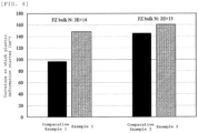
FIG. 4 shows a comparison of the curvatures of the epitaxial substrates according to Examples 1 and 2 and Comparative Examples 1 and 2 at which plastic deformation starts. - Hereinafter, the present invention will be described in detail, but the present invention is not limited thereto.
- As described above, in order to suppress the occurrence of warpage abnormality and bonding failure, a silicon single crystal substrate for vapor phase growth that is hard to be plastically deformed has been required.
- As a result of diligent studies on the above problems, the inventors of the present invention have found that a silicon single crystal substrate for vapor phase growth, comprising the silicon single crystal substrate being made of an FZ crystal having a resistivity of 1000 Qcm or more, wherein the surface of the silicon single crystal substrate is provided with a high nitrogen concentration layer having a nitrogen concentration higher than that of other regions and a nitrogen concentration of 5 × 10¹⁵ atoms/cm3 or more and a thickness of 10 to 100 µm, is suitable for substrates for high frequency devices since the substrate reduces parasitic capacitance, and because the surface of the substrate contains a high concentration of nitrogen, it has excellent mechanical properties when a vapor phase growth layer of semiconductor single crystals is formed, plastic deformation is unlikely to occur, and the occurrence of warpage abnormality and bonding failure is suppressed and completed the present invention.
- The inventors of the present invention also have found that a method for producing a silicon single crystal substrate for vapor phase growth, wherein a silicon single crystal substrate having a resistivity of 1000 Qcm or more manufactured by the FZ method is subjected to RTA treatment in a nitrogen-containing gas atmosphere, to form a high nitrogen concentration layer having a nitrogen concentration higher than that of other regions and a nitrogen concentration of 5 × 10¹⁵ atoms/cm3 or more and a thickness of 10 to 100 um at the surface of the silicon single crystal substrate, that is suitable for a substrate for a high frequency device, and the surface of the silicon single crystal substrate for vapor phase growth contains a high concentration of nitrogen, it has excellent mechanical properties, when a vapor phase growth layer of semiconductor single crystals is formed, it is resistant to plastic deformation and it can suppress the occurrence of warpage abnormality and bonding failure, can be produced easily and completed the present invention.
- Hereinafter, an embodiment of a silicon single crystal substrate for vapor phase growth, a vapor phase growth substrate, and methods for producing them according to the present invention will be described with reference to
FIGS. 1 to 3 . -
FIG. 1 shows a conceptual diagram of a silicon single crystal substrate for vapor phase growth according to the present invention. As the siliconsingle crystal substrate 10 for vapor phase growth according to the present invention, in order to reduce the leakage current through the substrate, a single crystal ingot manufactured by the FZ method, which is less affected by the thermal donor, is sliced into a wafer shape, and a silicon single crystal substrate composed of a FZ crystal and having a resistivity of 1000 Qcm or more is used. Here, the upper limit of the resistivity of the silicon single crystal substrate is not particularly limited, but may be, for example, 10 kQcm or less. Further, the siliconsingle crystal substrate 10 for vapor phase growth according to the present invention has a highnitrogen concentration layer 1 at the front surface, which has higher nitrogen concentration than that of other regions (bulk or back surface), and the nitrogen concentration is 5 × 10¹⁵ atoms/cm3 or more, and the thickness of the highnitrogen concentration layer 1 is 10 to 100 um. The upper limit of the nitrogen concentration of the highnitrogen concentration layer 1 can be 5 × 10¹⁶ atoms/cm3. Further, a plurality of highnitrogen concentration layers 1 may be formed by changing the concentration. A trap-rich layer that degrades the carrier lifetime may be formed on the surface of the siliconsingle crystal substrate 10. -
FIG. 2 shows a conceptual diagram of a vapor phase growth substrate according to the present invention. The vaporphase growth substrate 20 according to the present invention has the vaporphase growth layer 2 of the semiconductor single crystal on the highnitrogen concentration layer 1 of the siliconsingle crystal substrate 10. The vaporphase growth layer 2 is formed by vapor phase growth such as a thermal CVD method, a MOVPE method, an MBE method, a vacuum vapor deposition method, and a sputtering method, and functions as a device layer, for example. - The composition, film thickness, or the like of the vapor
phase growth layer 2 of the semiconductor single crystal are not particularly limited. For example, silicon thin film, silicon carbide, and nitride (group III-V) semiconductors such as GaN, AlN, InN, AlGaN, InGaN, AlInN, and AlScN can be used. The film thickness can be, for example, 1 to 10 um, and can be designed according to the device. - Further, as shown in
FIG. 2 , anintermediate layer 3 may be provided. Theintermediate layer 3 functions as a buffer layer inserted for improving the crystallinity of the device layer and controlling the stress. Theintermediate layer 3 may be omitted when there is no need to improve stress or crystallinity, such as silicon homo-epitaxial. On the other hand, due to the configuration of a device such as a high frequency filter, it may be made of a metal that can be used as a sacrificial layer for creating a spacer or an electrode. -
FIG. 3 shows a conceptual diagram of another example of a vaporphase growth substrate 30 according to the present invention. For example, in the high mobility transistor (HEMT) structure shown inFIG. 3 , the vaporphase growth layer 2 that functions as a device layer is composed of agallium nitride 2a and anelectron supply layer 2b made of AlGaN formed on thegallium nitride 2a. The vaporphase growth layer 2 is preferably a crystal having few crystal defects and few impurities such as carbon and oxygen in order to improve device characteristics. - Gallium nitride has a lattice constant difference of 17% and a thermal expansion coefficient difference of 116% from that of a silicon (111) single crystal, and stress is applied to a thin film or a substrate during the growth at a high temperature. Further, since the wafer is usually heated to 1000 °C or higher during the growth, when the wafer is stressed, it does not break brittlely and exhibits ductility, causing dislocations and plastic deformation.
- The silicon single crystal substrate according to the present invention is suitable as a substrate for high frequency devices because the parasitic capacitance is reduced. Further, since the surface of the substrate contains a high concentration of nitrogen, it has excellent mechanical properties. Therefore, when forming a vapor phase growth layer of a semiconductor single crystal, it is possible to prevent the propagation of dislocations of the silicon single crystal substrate and prevent plastic deformation. Then, by preventing the plastic deformation, it is possible to reduce the warp abnormality and improve the yield. In addition, since the substrate can withstand stress, the film thickness of the vapor phase growth layer can be increased, and the degree of freedom in device design is improved.
- In the silicon
single crystal substrate 10 for vapor phase growth as described above, first, a silicon single crystal ingot having a resistivity of 1000 Qcm or more is manufactured by the FZ method, and the ingot is sliced into wafers to form a silicon single crystal substrate. The substrate is produced by a method of injecting nitrogen by performing RTA (Rapid Thermal Annealing) treatment in a nitrogen-containing gas atmosphere such as ammonia gas. The conditions for the RTA treatment are not particularly limited, and may be any conditions as long as the nitrogen concentration and thickness of the highnitrogen concentration layer 1 are within the above ranges. - When the above treatment is performed, a silicon nitride layer by RTA treatment is formed on the high
nitrogen concentration layer 1, and this silicon nitride layer can be removed by etching or polishing. In the next step, it is essential to remove the nitride layer by etching or polishing on the side where the intermediate layer or the vapor phase growth layer of the semiconductor single crystal is formed, but the silicon nitride layer may remain on the back surface and the edge surface, or it may be removed. Further, when the trap-rich layer is formed, the method for forming the trap-rich layer is not particularly limited, but it can be formed by ion implantation or irradiation with ionizing radiation such as electron beam, X-ray, and γ-ray. - The vapor
phase growth substrate 20 according to the present invention can be produced by performing vapor phase growth, such as thermal CVD method, MOVPE method, MBE method, vacuum vapor deposition method, and sputtering method, a semiconductor single crystal vaporphase growth layer 2 on the highnitrogen concentration layer 1 of the siliconsingle crystal substrate 10 via anintermediate layer 3 if necessary. In the above-mentioned HEMT example, when GaN or AlGaN is formed as the vaporphase growth layer 2, it can be produced at a growth temperature of 900 °C to 1350 °C by using, for example, the MOVPE method. These vapor phase growth conditions may be carried out under generally used conditions. - Hereinafter, the present invention will be specifically described with reference to examples, but this does not limit the present invention.
- First, two types of wafers, which were silicon single crystal substrates composed of FZ crystals having a diameter of 6 inches (150 mm), a plane orientation (111), and a resistivity of 1000 Qcm or more, and having different nitrogen concentrations, were prepared. As a result of analyzing each nitrogen concentration by FT-IR and SIMS measurement, the substrate having a low nitrogen concentration was 3.0 × 10¹⁴ atoms/cm3, and the substrate having a high nitrogen concentration was 2.0 × 10¹⁵ atoms/cm3.
- A silicon single crystal substrate having a nitrogen concentration of 3.0 × 10¹⁴ atoms/cm3 was used, and nitrogen was injected into the surface layer by heat treatment by the RTA method. The RTA treatment conditions were 1250 °C and 10 sec in an NH3 and Ar atmosphere, and a high nitrogen concentration layer having a nitrogen concentration of 5 × 10¹⁵ /cm3 and a thickness of 38 µm was formed at the surface layer of the silicon single crystal substrate. After the RTA treatment, the silicon nitride film was removed by HF cleaning. Then, GaN, as a nitride semiconductor, was epitaxially grown by the MOVPE method. An epitaxial layer having a total film thickness of 4.5 um was grown at a growth temperature of 1000 to 1200 °C. For epitaxial growth, the growth substrates prepared in each of Example 1, Example 2 and Comparative Examples 1 and 2 described below were carried out in the same MOVPE furnace.
- An epitaxial layer of GaN, as a nitride semiconductor, was formed in the same manner as in Example 1 except that a silicon single crystal substrate having a nitrogen concentration of 2.0 × 10¹⁵ atoms/cm3 was used.
- Using the same silicon single crystal substrate as in Example 1, an epitaxial layer was formed without performing RTA treatment (without forming a high nitrogen concentration layer).
- Using the same silicon single crystal substrate as in Example 2, an epitaxial layer was formed without performing RTA treatment (without forming a high nitrogen concentration layer).
- For the vapor phase growth substrates of Examples 1 and 2 and Comparative Examples 1 and 2 in which the epitaxial layer was formed as described above, the curvatures at which plastic deformation started were compared. For this evaluation, EpiCurve TT manufactured by LAYTEC was used as a measuring device, and the curvature of the wafer during the growth was measured by incident two laser beams in parallel into the chamber and changing the position of the reflected laser spot.
- The results are shown in
FIG. 4 . As shown inFIG. 4 , it was found that regardless of the nitrogen concentration in the bulk, by performing the RTA treatment to form a high nitrogen concentration layer, the curvature at which plastic deformation started during the vapor phase growth of the semiconductor single crystal layer became large and the yield stress became large. In particular, a large improvement was seen in the samples with low bulk nitrogen concentration. - The present invention is not limited to the above embodiment. The above-described embodiment is an example, and any examples having substantially the same structure and having the same effect as the technical idea described in the claims of the present invention are included in the technical scope of the present invention.
Claims (6)
- A silicon single crystal substrate for vapor phase growth,comprising the silicon single crystal substrate being made of an FZ crystal having a resistivity of 1000 Qcm or more,wherein the surface of the silicon single crystal substrate is provided with a high nitrogen concentration layer having a nitrogen concentration higher than that of other regions and a nitrogen concentration of 5 × 10¹⁵ atoms/cm3 or more and a thickness of 10 to 100 µm.
- A vapor phase growth substrate, wherein a vapor phase growth layer of a semiconductor single crystal is provided on the silicon single crystal substrate according to claim 1.
- The vapor phase growth substrate according to claim 2, wherein the vapor phase growth layer of the semiconductor single crystal contains a nitride semiconductor.
- A method for producing a silicon single crystal substrate for vapor phase growth,
wherein a silicon single crystal substrate having a resistivity of 1000 Ωcm or more manufactured by the FZ method is subjected to RTA treatment in a nitrogen-containing gas atmosphere, to form a high nitrogen concentration layer having a nitrogen concentration higher than that of other regions and a nitrogen concentration of 5 × 10¹⁵ atoms/cm3 or more and a thickness of 10 to 100 um at the surface of the silicon single crystal substrate. - A method for producing a vapor phase growth substrate, which comprises growing a semiconductor single crystal layer in vapor phase on the substrate for vapor phase growth produced by the method for producing a substrate for vapor phase growth according to claim 4.
- The method for producing a vapor phase growth substrate according to claim 5, wherein the semiconductor single crystal layer contains a nitride semiconductor.
Applications Claiming Priority (2)
| Application Number | Priority Date | Filing Date | Title |
|---|---|---|---|
| JP2020073795A JP7173082B2 (en) | 2020-04-17 | 2020-04-17 | Silicon single crystal substrate for vapor phase epitaxy, vapor phase epitaxy substrate, and manufacturing method thereof |
| PCT/JP2021/011845 WO2021210354A1 (en) | 2020-04-17 | 2021-03-23 | Silicon single crystal substrate for vapor deposition, vapor deposition substrate, and manufacturing methods therefor |
Publications (2)
| Publication Number | Publication Date |
|---|---|
| EP4137617A1 true EP4137617A1 (en) | 2023-02-22 |
| EP4137617A4 EP4137617A4 (en) | 2024-06-05 |
Family
ID=78084253
Family Applications (1)
| Application Number | Title | Priority Date | Filing Date |
|---|---|---|---|
| EP21787666.3A Pending EP4137617A4 (en) | 2020-04-17 | 2021-03-23 | SINGLE CRYSTAL SILICON SUBSTRATE FOR VAPOR DEPOSITION, VAPOR DEPOSITION SUBSTRATE AND ASSOCIATED MANUFACTURING PROCESSES |
Country Status (6)
| Country | Link |
|---|---|
| US (1) | US12606935B2 (en) |
| EP (1) | EP4137617A4 (en) |
| JP (1) | JP7173082B2 (en) |
| CN (1) | CN115398042B (en) |
| TW (1) | TWI894244B (en) |
| WO (1) | WO2021210354A1 (en) |
Families Citing this family (2)
| Publication number | Priority date | Publication date | Assignee | Title |
|---|---|---|---|---|
| US20240035195A1 (en) * | 2022-07-29 | 2024-02-01 | Applied Materials, Inc. | Methods, systems, and apparatus for forming layers having single crystalline structures |
| JP2024179276A (en) * | 2023-06-14 | 2024-12-26 | 株式会社Sumco | Silicon wafer and its manufacturing method |
Family Cites Families (17)
| Publication number | Priority date | Publication date | Assignee | Title |
|---|---|---|---|---|
| JP4218681B2 (en) * | 2003-07-29 | 2009-02-04 | 信越半導体株式会社 | Silicon single crystal substrate manufacturing method, resistance characteristic measuring method, and resistance characteristic guarantee method |
| JP4794137B2 (en) | 2004-04-23 | 2011-10-19 | Sumco Techxiv株式会社 | Heat treatment method for silicon semiconductor substrate |
| JP2006186245A (en) * | 2004-12-28 | 2006-07-13 | Tokyo Electron Ltd | Method of nitriding tunnel oxide film, method of manufacturing nonvolatile memory element, nonvolatile memory element, computer program, and recording medium |
| JP2007176725A (en) | 2005-12-27 | 2007-07-12 | Shin Etsu Handotai Co Ltd | Method for manufacturing neutron-irradiated silicon single crystal |
| JP2011054656A (en) * | 2009-08-31 | 2011-03-17 | Sumco Corp | High resistivity silicon wafer and manufacturing method thereof |
| JP5159858B2 (en) | 2010-09-08 | 2013-03-13 | コバレントマテリアル株式会社 | Gallium nitride compound semiconductor substrate and manufacturing method thereof |
| JP5817127B2 (en) | 2011-01-21 | 2015-11-18 | 株式会社Sumco | Semiconductor substrate and manufacturing method thereof |
| JP2014236093A (en) * | 2013-05-31 | 2014-12-15 | サンケン電気株式会社 | Silicon-based substrate, semiconductor device and method for manufacturing semiconductor device |
| DE102014217605A1 (en) * | 2014-09-03 | 2016-03-03 | Siltronic Ag | A method of supporting a growing single crystal during crystallization of the single crystal according to the FZ method |
| JP6245156B2 (en) * | 2014-12-02 | 2017-12-13 | 信越半導体株式会社 | Silicon wafer evaluation method |
| CN105280491A (en) * | 2015-06-17 | 2016-01-27 | 上海超硅半导体有限公司 | Silicon chip and preparing method |
| KR102439602B1 (en) * | 2016-06-08 | 2022-09-01 | 글로벌웨이퍼스 씨오., 엘티디. | Single-crystal silicon ingots with high resistivity and wafers with improved mechanical strength |
| JP6299835B1 (en) * | 2016-10-07 | 2018-03-28 | 株式会社Sumco | Epitaxial silicon wafer and method of manufacturing epitaxial silicon wafer |
| KR20190011475A (en) * | 2017-07-25 | 2019-02-07 | 에스케이실트론 주식회사 | Method for manufacturing a wafer and the wafer |
| JP2020098839A (en) * | 2018-12-17 | 2020-06-25 | 信越半導体株式会社 | Nitride semiconductor wafer manufacturing method and nitride semiconductor wafer |
| JP7279552B2 (en) * | 2019-07-11 | 2023-05-23 | 信越半導体株式会社 | Substrate for electronic device and manufacturing method thereof |
| WO2021129270A1 (en) * | 2019-12-24 | 2021-07-01 | 山东天岳先进科技股份有限公司 | Silicon carbide single crystal, substrate and device for preparation |
-
2020
- 2020-04-17 JP JP2020073795A patent/JP7173082B2/en active Active
-
2021
- 2021-03-23 US US17/918,713 patent/US12606935B2/en active Active
- 2021-03-23 EP EP21787666.3A patent/EP4137617A4/en active Pending
- 2021-03-23 WO PCT/JP2021/011845 patent/WO2021210354A1/en not_active Ceased
- 2021-03-23 CN CN202180028335.2A patent/CN115398042B/en active Active
- 2021-03-30 TW TW110111444A patent/TWI894244B/en active
Also Published As
| Publication number | Publication date |
|---|---|
| TWI894244B (en) | 2025-08-21 |
| US12606935B2 (en) | 2026-04-21 |
| EP4137617A4 (en) | 2024-06-05 |
| WO2021210354A1 (en) | 2021-10-21 |
| JP2021169397A (en) | 2021-10-28 |
| CN115398042A (en) | 2022-11-25 |
| CN115398042B (en) | 2024-05-03 |
| JP7173082B2 (en) | 2022-11-16 |
| US20230235481A1 (en) | 2023-07-27 |
| TW202140843A (en) | 2021-11-01 |
Similar Documents
| Publication | Publication Date | Title |
|---|---|---|
| WO2020129540A1 (en) | Method for manufacturing nitride semiconductor wafer and nitride semiconductor wafer | |
| US20240297245A1 (en) | Integrated circuit, manufacturing method thereof, power amplifier, and electronic device | |
| US12610599B2 (en) | Nitride semiconductor wafer and method for producing nitride semiconductor wafer | |
| US12606935B2 (en) | Silicon single crystal substrate for vapor phase growth, vapor phase growth substrate and methods for producing them | |
| KR20190074774A (en) | Methode for manufacturing gallium nitride substrate using a ultra-thin sapphire substrate | |
| JP7142184B2 (en) | Nitride semiconductor wafer manufacturing method and nitride semiconductor wafer | |
| JP5439675B2 (en) | Nitride semiconductor substrate and nitride semiconductor | |
| JP2011100860A (en) | Ion-implanted group-iii nitride semiconductor substrate, bonding substrate for group-iii nitride semiconductor layer, and method for manufacturing group-iii nitride semiconductor device | |
| CN115398044B (en) | Semiconductor substrate manufacturing methods, semiconductor substrates, and methods for suppressing crack formation in the growth layer. | |
| EP4589057A1 (en) | Single crystal silicon substrate equipped with nitride semiconductor layer, and method for manufacturing single crystal silicon substrate equipped with nitride semiconductor layer | |
| EP4462465A1 (en) | Nitride semiconductor substrate and method for producing same | |
| JP2007142003A (en) | Manufacturing method of group iii nitride crystal, epitaxial substrate, warpage reduction method therein, and semiconductor element | |
| KR101480949B1 (en) | Compound semiconductor substrate and method for fabricating the same | |
| KR20230142717A (en) | Nitride semiconductor substrate and manufacturing method thereof |
Legal Events
| Date | Code | Title | Description |
|---|---|---|---|
| STAA | Information on the status of an ep patent application or granted ep patent |
Free format text: STATUS: THE INTERNATIONAL PUBLICATION HAS BEEN MADE |
|
| PUAI | Public reference made under article 153(3) epc to a published international application that has entered the european phase |
Free format text: ORIGINAL CODE: 0009012 |
|
| STAA | Information on the status of an ep patent application or granted ep patent |
Free format text: STATUS: REQUEST FOR EXAMINATION WAS MADE |
|
| 17P | Request for examination filed |
Effective date: 20221013 |
|
| AK | Designated contracting states |
Kind code of ref document: A1 Designated state(s): AL AT BE BG CH CY CZ DE DK EE ES FI FR GB GR HR HU IE IS IT LI LT LU LV MC MK MT NL NO PL PT RO RS SE SI SK SM TR |
|
| DAV | Request for validation of the european patent (deleted) | ||
| DAX | Request for extension of the european patent (deleted) | ||
| A4 | Supplementary search report drawn up and despatched |
Effective date: 20240503 |
|
| RIC1 | Information provided on ipc code assigned before grant |
Ipc: C30B 29/40 20060101ALI20240427BHEP Ipc: C30B 33/02 20060101ALI20240427BHEP Ipc: C30B 25/18 20060101ALI20240427BHEP Ipc: C30B 13/00 20060101ALI20240427BHEP Ipc: C23C 16/30 20060101ALI20240427BHEP Ipc: C30B 29/06 20060101AFI20240427BHEP |