EP4135122A1 - Wiring board and method for manufacturing wiring board - Google Patents
Wiring board and method for manufacturing wiring board Download PDFInfo
- Publication number
- EP4135122A1 EP4135122A1 EP21784598.1A EP21784598A EP4135122A1 EP 4135122 A1 EP4135122 A1 EP 4135122A1 EP 21784598 A EP21784598 A EP 21784598A EP 4135122 A1 EP4135122 A1 EP 4135122A1
- Authority
- EP
- European Patent Office
- Prior art keywords
- layer
- wiring
- substrate
- wiring board
- mesh
- Prior art date
- Legal status (The legal status is an assumption and is not a legal conclusion. Google has not performed a legal analysis and makes no representation as to the accuracy of the status listed.)
- Pending
Links
Images



Classifications
-
- H—ELECTRICITY
- H01—ELECTRIC ELEMENTS
- H01Q—ANTENNAS, i.e. RADIO AERIALS
- H01Q9/00—Electrically-short antennas having dimensions not more than twice the operating wavelength and consisting of conductive active radiating elements
- H01Q9/04—Resonant antennas
- H01Q9/0407—Substantially flat resonant element parallel to ground plane, e.g. patch antenna
-
- H—ELECTRICITY
- H05—ELECTRIC TECHNIQUES NOT OTHERWISE PROVIDED FOR
- H05K—PRINTED CIRCUITS; CASINGS OR CONSTRUCTIONAL DETAILS OF ELECTRIC APPARATUS; MANUFACTURE OF ASSEMBLAGES OF ELECTRICAL COMPONENTS
- H05K1/00—Printed circuits
- H05K1/02—Details
-
- H—ELECTRICITY
- H01—ELECTRIC ELEMENTS
- H01Q—ANTENNAS, i.e. RADIO AERIALS
- H01Q1/00—Details of, or arrangements associated with, antennas
- H01Q1/36—Structural form of radiating elements, e.g. cone, spiral, umbrella; Particular materials used therewith
- H01Q1/38—Structural form of radiating elements, e.g. cone, spiral, umbrella; Particular materials used therewith formed by a conductive layer on an insulating support
-
- H—ELECTRICITY
- H01—ELECTRIC ELEMENTS
- H01Q—ANTENNAS, i.e. RADIO AERIALS
- H01Q21/00—Antenna arrays or systems
- H01Q21/0087—Apparatus or processes specially adapted for manufacturing antenna arrays
- H01Q21/0093—Monolithic arrays
-
- H—ELECTRICITY
- H01—ELECTRIC ELEMENTS
- H01Q—ANTENNAS, i.e. RADIO AERIALS
- H01Q21/00—Antenna arrays or systems
- H01Q21/28—Combinations of substantially independent non-interacting antenna units or systems
-
- H—ELECTRICITY
- H01—ELECTRIC ELEMENTS
- H01Q—ANTENNAS, i.e. RADIO AERIALS
- H01Q5/00—Arrangements for simultaneous operation of antennas on two or more different wavebands, e.g. dual-band or multi-band arrangements
- H01Q5/20—Arrangements for simultaneous operation of antennas on two or more different wavebands, e.g. dual-band or multi-band arrangements characterised by the operating wavebands
- H01Q5/22—RF wavebands combined with non-RF wavebands, e.g. infrared or optical
-
- H—ELECTRICITY
- H05—ELECTRIC TECHNIQUES NOT OTHERWISE PROVIDED FOR
- H05K—PRINTED CIRCUITS; CASINGS OR CONSTRUCTIONAL DETAILS OF ELECTRIC APPARATUS; MANUFACTURE OF ASSEMBLAGES OF ELECTRICAL COMPONENTS
- H05K1/00—Printed circuits
- H05K1/02—Details
- H05K1/0274—Optical details, e.g. printed circuits comprising integral optical means
-
- H—ELECTRICITY
- H05—ELECTRIC TECHNIQUES NOT OTHERWISE PROVIDED FOR
- H05K—PRINTED CIRCUITS; CASINGS OR CONSTRUCTIONAL DETAILS OF ELECTRIC APPARATUS; MANUFACTURE OF ASSEMBLAGES OF ELECTRICAL COMPONENTS
- H05K1/00—Printed circuits
- H05K1/02—Details
- H05K1/09—Use of materials for the conductive, e.g. metallic pattern
-
- H—ELECTRICITY
- H05—ELECTRIC TECHNIQUES NOT OTHERWISE PROVIDED FOR
- H05K—PRINTED CIRCUITS; CASINGS OR CONSTRUCTIONAL DETAILS OF ELECTRIC APPARATUS; MANUFACTURE OF ASSEMBLAGES OF ELECTRICAL COMPONENTS
- H05K3/00—Apparatus or processes for manufacturing printed circuits
- H05K3/22—Secondary treatment of printed circuits
- H05K3/24—Reinforcing of the conductive pattern
- H05K3/244—Finish plating of conductors, especially of copper conductors, e.g. for pads or lands
-
- H—ELECTRICITY
- H05—ELECTRIC TECHNIQUES NOT OTHERWISE PROVIDED FOR
- H05K—PRINTED CIRCUITS; CASINGS OR CONSTRUCTIONAL DETAILS OF ELECTRIC APPARATUS; MANUFACTURE OF ASSEMBLAGES OF ELECTRICAL COMPONENTS
- H05K3/00—Apparatus or processes for manufacturing printed circuits
- H05K3/38—Improvement of the adhesion between the insulating substrate and the metal
- H05K3/381—Improvement of the adhesion between the insulating substrate and the metal by special treatment of the substrate
-
- H—ELECTRICITY
- H01—ELECTRIC ELEMENTS
- H01Q—ANTENNAS, i.e. RADIO AERIALS
- H01Q1/00—Details of, or arrangements associated with, antennas
- H01Q1/40—Radiating elements coated with or embedded in protective material
-
- H—ELECTRICITY
- H05—ELECTRIC TECHNIQUES NOT OTHERWISE PROVIDED FOR
- H05K—PRINTED CIRCUITS; CASINGS OR CONSTRUCTIONAL DETAILS OF ELECTRIC APPARATUS; MANUFACTURE OF ASSEMBLAGES OF ELECTRICAL COMPONENTS
- H05K1/00—Printed circuits
- H05K1/16—Printed circuits incorporating printed electric components, e.g. printed resistors, capacitors or inductors
- H05K1/165—Printed circuits incorporating printed electric components, e.g. printed resistors, capacitors or inductors incorporating printed inductors
-
- H—ELECTRICITY
- H05—ELECTRIC TECHNIQUES NOT OTHERWISE PROVIDED FOR
- H05K—PRINTED CIRCUITS; CASINGS OR CONSTRUCTIONAL DETAILS OF ELECTRIC APPARATUS; MANUFACTURE OF ASSEMBLAGES OF ELECTRICAL COMPONENTS
- H05K2201/00—Indexing scheme relating to printed circuits covered by H05K1/00
- H05K2201/01—Dielectrics
- H05K2201/0104—Properties and characteristics in general
- H05K2201/0108—Transparent
-
- H—ELECTRICITY
- H05—ELECTRIC TECHNIQUES NOT OTHERWISE PROVIDED FOR
- H05K—PRINTED CIRCUITS; CASINGS OR CONSTRUCTIONAL DETAILS OF ELECTRIC APPARATUS; MANUFACTURE OF ASSEMBLAGES OF ELECTRICAL COMPONENTS
- H05K2201/00—Indexing scheme relating to printed circuits covered by H05K1/00
- H05K2201/03—Conductive materials
- H05K2201/0332—Structure of the conductor
- H05K2201/0335—Layered conductors or foils
- H05K2201/0338—Layered conductor, e.g. layered metal substrate, layered finish layer or layered thin film adhesion layer
-
- H—ELECTRICITY
- H05—ELECTRIC TECHNIQUES NOT OTHERWISE PROVIDED FOR
- H05K—PRINTED CIRCUITS; CASINGS OR CONSTRUCTIONAL DETAILS OF ELECTRIC APPARATUS; MANUFACTURE OF ASSEMBLAGES OF ELECTRICAL COMPONENTS
- H05K2201/00—Indexing scheme relating to printed circuits covered by H05K1/00
- H05K2201/09—Shape and layout
- H05K2201/09209—Shape and layout details of conductors
- H05K2201/09654—Shape and layout details of conductors covering at least two types of conductors provided for in H05K2201/09218 - H05K2201/095
- H05K2201/09681—Mesh conductors, e.g. as a ground plane
-
- H—ELECTRICITY
- H05—ELECTRIC TECHNIQUES NOT OTHERWISE PROVIDED FOR
- H05K—PRINTED CIRCUITS; CASINGS OR CONSTRUCTIONAL DETAILS OF ELECTRIC APPARATUS; MANUFACTURE OF ASSEMBLAGES OF ELECTRICAL COMPONENTS
- H05K2201/00—Indexing scheme relating to printed circuits covered by H05K1/00
- H05K2201/10—Details of components or other objects attached to or integrated in a printed circuit board
- H05K2201/10007—Types of components
- H05K2201/10098—Components for radio transmission, e.g. radio frequency identification [RFID] tag, printed or non-printed antennas
-
- H—ELECTRICITY
- H05—ELECTRIC TECHNIQUES NOT OTHERWISE PROVIDED FOR
- H05K—PRINTED CIRCUITS; CASINGS OR CONSTRUCTIONAL DETAILS OF ELECTRIC APPARATUS; MANUFACTURE OF ASSEMBLAGES OF ELECTRICAL COMPONENTS
- H05K3/00—Apparatus or processes for manufacturing printed circuits
- H05K3/10—Apparatus or processes for manufacturing printed circuits in which conductive material is applied to the insulating support in such a manner as to form the desired conductive pattern
- H05K3/108—Apparatus or processes for manufacturing printed circuits in which conductive material is applied to the insulating support in such a manner as to form the desired conductive pattern by semi-additive methods; masks therefor
-
- H—ELECTRICITY
- H05—ELECTRIC TECHNIQUES NOT OTHERWISE PROVIDED FOR
- H05K—PRINTED CIRCUITS; CASINGS OR CONSTRUCTIONAL DETAILS OF ELECTRIC APPARATUS; MANUFACTURE OF ASSEMBLAGES OF ELECTRICAL COMPONENTS
- H05K3/00—Apparatus or processes for manufacturing printed circuits
- H05K3/38—Improvement of the adhesion between the insulating substrate and the metal
- H05K3/386—Improvement of the adhesion between the insulating substrate and the metal by the use of an organic polymeric bonding layer, e.g. adhesive
Definitions
- An embodiment of the present disclosure relates to a wiring board and a method for manufacturing the wiring board.
- a portable terminal device may include a plurality of antennas including a telephone antenna, a wireless fidelity (WiFi) antenna, a third generation (3G) antenna, a fourth generation (4G) antenna, a long term evolution (LTE) antenna, a Bluetooth (registered trademark) antenna, and a near field communication (NFC) antenna.
- WiFi wireless fidelity
- 3G third generation
- 4G fourth generation
- LTE long term evolution
- NFC near field communication
- a film antenna is a transparent antenna including a transparent base material on which an antenna pattern is formed.
- the antenna pattern is formed of a conductor mesh layer having a mesh structure, which includes a conductor portion composed of an opaque conductor layer and a plurality of openings in which no conductor layer is formed.
- the film antenna according to the related art includes a transparent base material on which a mesh wiring layer (conductor mesh layer) is provided.
- the mesh wiring layer may be readily visible to the naked eye when the mesh wiring layer easily reflects visible light.
- the present embodiment provides a wiring board having a mesh wiring layer that is not readily visible to the naked eye and a method for manufacturing the wiring board.
- a wiring board includes a substrate and a mesh wiring layer disposed on the substrate and including a plurality of wiring lines.
- the substrate has a transmittance of 85% or more for light with a wavelength of 380 nm or more and 750 nm or less.
- Each of the wiring lines includes a metal layer and a blackened layer disposed on the metal layer.
- the blackened layer has a thickness of 5 nm or more and 100 nm or less.
- the blackened layer may include palladium or tellurium.
- the blackened layer may be obtained by subjecting the metal layer to an oxidation process.
- the blackened layer may include an oxide of a metal contained in the metal layer.
- the mesh wiring layer may be an antenna.
- the metal layer may include gold, silver, copper, platinum, tin, aluminum, iron, or nickel.
- the substrate may have a dielectric loss tangent of 0.002 or less.
- the substrate may have a thickness of 5 ⁇ m or more and 200 ⁇ m or less.
- the substrate may include cycloolefin polymer or polynorbornene polymer.
- the mesh wiring layer may be provided only on a portion of the su bstrate.
- a method for manufacturing a wiring board includes a step of preparing a substrate and a step of forming a mesh wiring layer including a plurality of wiring lines on the substrate.
- the substrate has a transmittance of 85% or more for light with a wavelength of 380 nm or more and 750 nm or less.
- Each of the wiring lines includes a metal layer and a blackened layer disposed on the metal layer.
- the blackened layer has a thickness of 5 nm or more and 100 nm or less.
- the step of forming the mesh wiring layer may include a step of forming the metal layer and a step of forming the blackened layer on the metal layer, the blackened layer including palladium or tellurium.
- the step of forming the mesh wiring layer may include a step of forming the metal layer and a step of subjecting the metal layer to an oxidation process to form the blackened layer.
- the blackened layer may include an oxide of a metal contained in the metal layer.
- the mesh wiring layer may be an antenna.
- the metal layer may include gold, silver, copper, platinum, tin, aluminum, iron, or nickel.
- the substrate may have a dielectric loss tangent of 0.002 or less.
- the substrate may have a thickness of 5 ⁇ m or more and 200 ⁇ m or less.
- the substrate may include cycloolefin polymer or polynorbornene polymer.
- the mesh wiring layer may be provided only on a portion of the substrate.
- the mesh wiring layer is not readily visible to the naked eye.
- FIG. 1 to 9 illustrate the present embodiment.
- an "X direction” is a direction parallel to one side of a substrate.
- a “Y direction” is a direction perpendicular to the X direction and parallel to another side of the substrate.
- a “Z direction” is a direction perpendicular to both the X direction and the Y direction and parallel to a thickness direction of a wiring board.
- a “front surface” is a surface that faces in a positive Z direction and on which wiring lines are provided on the substrate.
- a “back surface” is a surface that faces in a negative Z direction and that is opposite to the surface on which the wiring lines are provided on the substrate.
- Figs. 1 to 5 illustrate the wiring board according to the present embodiment.
- a wiring board 10 is disposed on, for example, a display of an image display device.
- the wiring board 10 includes a transparent substrate 11 and mesh wiring layers (wiring pattern regions) 20 arranged on the substrate 11.
- the mesh wiring layers 20 are electrically connected to a feeding unit 40.
- the substrate 11 is substantially rectangular in plan view.
- the longitudinal direction of the substrate 11 is parallel to the Y direction, and the transverse direction of the substrate 11 is parallel to the X direction.
- the substrate 11, which is transparent, is substantially flat plate-shaped, and has a substantially uniform thickness over the entirety thereof.
- a length L 1 of the substrate 11 in the longitudinal direction (Y direction) may be selected from the range of, for example, 2 mm or more and 300 mm or less, preferably from the range of 100 mm or more and 200 mm or less.
- a length L 2 of the substrate 11 in the transverse direction (X direction) may be selected from the range of, for example, 2 mm or more and 300 mm or less, preferably from the range of 50 mm or more and 100 mm or less.
- the substrate 11 may have rounded corners.
- the material of the substrate 11 may be any material that is transparent in the visible light range and that has electrically insulating properties.
- the material of the substrate 11 is polyethylene terephthalate in the present embodiment, but is not limited to this.
- the material of the substrate 11 is preferably an organic insulating material, for example, a polyester-based resin such as polyethylene terephthalate, an acrylic resin such as polymethyl methacrylate, a polycarbonate-based resin, a polyimide-based resin, a polyolefin-based resin such as cycloolefin polymer, or a cellulose-based resin material such as triacetyl cellulose.
- the material of the substrate 11 may be an organic insulating material such as cycloolefin polymer (for example, ZF-16 produced by Zeon Corporation) or polynorbornene polymer (produced by Sumitomo Bakelite Co., Ltd.).
- the material of the substrate 11 may instead be glass, ceramic, etc., as appropriate depending on the use.
- the substrate 11 is composed of a single layer in the illustrated example, the substrate 11 is not limited to this, and may instead have a multilayer structure including a plurality of base materials or layers.
- the substrate 11 may be film-shaped or plate-shaped.
- the thickness of the substrate 11 is not particularly limited, and may be selected as appropriate depending on the use.
- a thickness (in the Z direction) T 1 of the substrate 11 may be in the range of, for example, 5 ⁇ m or more and 200 ⁇ m or less.
- the substrate 11 may have a dielectric loss tangent of 0.002 or less, preferably 0.001 or less.
- the dielectric loss tangent of the substrate 11 has no particular lower limit, but may be more than 0.
- loss in gain (sensitivity) during transmission and reception of electromagnetic waves may be reduced, particularly in a case where high-frequency electromagnetic waves (for example, millimeter waves) are transmitted and received by the mesh wiring layers 20.
- the dielectric loss tangent of the substrate 11 has no particular lower limit.
- the dielectric constant of the substrate 11 is not particularly limited, and may instead be 2.0 or more and 10.0 or less.
- the dielectric loss tangent of the substrate 11 may be measured in accordance with IEC 62562. More specifically, first, a specimen is prepared by cutting out a portion of the substrate 11 on which no mesh wiring layers 20 are formed. Alternatively, a portion of the substrate 11 on which the mesh wiring layers 20 are formed may be cut out, and then the mesh wiring layers 20 may be removed by, for example, etching. The specimen has a width in the range of 10 mm to 20 mm and a length in the range of 50 mm to 100 mm. Next, the dielectric loss tangent is measured in accordance with IEC 62562. The dielectric constant and the dielectric loss tangent of the substrate 11 may also be measured in accordance with ASTM D150.
- the transmittance of the substrate 11 for visible light may be 85% or more, preferably 90% or more.
- the transmittance of the substrate 11 for visible light has no particular upper limit, but may be, for example, 100% or less.
- transparency of the wiring board 10 can be increased, and visibility of a display 91 of an image display device 90 (described below) can be enhanced.
- the visible light is light with a wavelength of 380 nm to 780 nm.
- the transmittance for visible light of 85% or more means that when the absorbance of the substrate 11 is measured with a known spectrophotometer (for example, spectrometer V-670 manufactured by JASCO Corporation), the transmittance is 85% or more over the entire wavelength range of 380 nm to 780 nm.
- a known spectrophotometer for example, spectrometer V-670 manufactured by JASCO Corporation
- the mesh wiring layers 20 are composed of antenna pattern regions having a function of an antenna.
- the mesh wiring layers 20 (three in number), which are formed on the substrate 11, correspond to different frequency bands. More specifically, the mesh wiring layers 20 have different lengths (lengths in the Y direction) L a , each of which corresponds to a specific frequency band. The mesh wiring layers 20 corresponding to frequency bands with lower frequencies have longer lengths L a .
- the wiring board 10 is disposed on a display 91 of an image display device 90 (see Fig.
- each mesh wiring layer 20 may correspond to, for example, a telephone antenna, a WiFi antenna, a 3G antenna, a 4G antenna, a 5G antenna, an LTE antenna, a Bluetooth (registered trademark) antenna, or an NFC antenna.
- the mesh wiring layers 20 may be formed such that the mesh wiring layers 20 do not extend over the entire region of the substrate 11 but exist only in partial regions on the substrate 11.
- Each mesh wiring layer 20 is substantially rectangular in plan view.
- the longitudinal direction of each mesh wiring layer 20 is parallel to the Y direction, and the transverse direction of each mesh wiring layer 20 is parallel to the X direction.
- a length L a of each mesh wiring layer 20 in the longitudinal direction (Y direction) may be selected from the range of, for example, 1 mm or more and 100 mm or less.
- a width W a of each mesh wiring layer 20 in the transverse direction (X direction) may be selected from the range of, for example, 1 mm or more and 10 mm or less.
- the mesh wiring layers 20 may be millimeter wave antennas. When the mesh wiring layers 20 are millimeter wave antennas, the length L a of each mesh wiring layer 20 may be selected from the range of 1 mm or more and 10 mm or less, preferably 1.5 mm or more and 5 mm or less.
- Each mesh wiring layer 20 includes metal lines that form a grid structure or a mesh structure having a pattern periodic in the X direction and the Y direction.
- each mesh wiring layer 20 has a pattern including portions extending in the X direction (second-direction wiring lines 22) and portions extending in the Y direction (first-direction wiring lines 21).
- each mesh wiring layer 20 includes the first-direction wiring lines (antenna wiring lines) 21 that provide the function of an antenna and the second-direction wiring lines (antenna-connecting wiring lines) 22 that connect the first-direction wiring lines 21. More specifically, the first-direction wiring lines 21 and the second-direction wiring lines 22 are integrated together to form a grid structure or a mesh structure. Each first-direction wiring line 21 extends in a direction corresponding to the frequency band of the antenna (longitudinal direction, Y direction), and each second-direction wiring line 22 extends in a direction orthogonal to the first-direction wiring lines 21 (width direction, X direction).
- the first-direction wiring lines 21 have the length L a corresponding to a predetermined frequency band (above-described length of the mesh wiring layer 20, see Fig. 1 ) to mainly provide the function of an antenna.
- the second-direction wiring lines 22 connect the first-direction wiring lines 21 to each other to suppress defects such as breakage of the first-direction wiring lines 21 or electrical disconnection between each first-direction wiring line 21 and the feeding unit 40.
- each mesh wiring layer 20 has a plurality of openings 23 that are each surrounded by adjacent ones of the first-direction wiring lines 21 and adjacent ones of the second-direction wiring lines 22.
- the first-direction wiring lines 21 and the second-direction wiring lines 22 are arranged at equal intervals. More specifically, the first-direction wiring lines 21 are arranged at equal intervals, and a pitch P 1 thereof may be in the range of, for example, 0.01 mm or more and 1 mm or less.
- the second-direction wiring lines 22 are arranged at equal intervals, and a pitch P 2 thereof may be in the range of, for example, 0.01 mm or more and 1 mm or less.
- first-direction wiring lines 21 and the second-direction wiring lines 22 are both arranged at equal intervals as described above, differences in size between the openings 23 can be reduced in each mesh wiring layer 20, so that the mesh wiring layer 20 is not readily visible to the naked eye.
- the pitch P 1 of the first-direction wiring lines 21 is equal to the pitch P 2 of the second-direction wiring lines 22.
- the openings 23 are substantially square in plan view, and the substrate 11, which is transparent, is exposed at each opening 23. Therefore, the overall transparency of the wiring board 10 can be increased by increasing the area of each opening 23.
- a length L 3 of each side of each opening 23 may be in the range of, for example, 0.01 mm or more and 1 mm or less.
- Each first-direction wiring line 21 and each second-direction wiring line 22 are orthogonal to each other, but may instead cross each other at an acute or obtuse angle.
- the openings 23 preferably have the same shape and the same size over the entire region, but the shapes and sizes thereof may vary depending on the location and are not necessarily the same over the entire region.
- each first-direction wiring line 21 has a substantially rectangular or square cross section in a direction perpendicular to the longitudinal direction thereof (cross section in the X direction).
- the cross-sectional shape of each first-direction wiring line 21 is substantially uniform in the longitudinal direction of the first-direction wiring line 21 (Y direction).
- each second-direction wiring line 22 has a substantially rectangular or square cross section in a direction perpendicular to the longitudinal direction thereof (cross section in the Y direction).
- the cross-sectional shape of each second-direction wiring line 22 is substantially the same as the above-described cross-sectional shape of each first-direction wiring line 21 (shape of cross section in the X direction).
- each second-direction wiring line 22 is substantially uniform in the longitudinal direction of the second-direction wiring line 22 (X direction).
- the cross-sectional shapes of each first-direction wiring line 21 and each second-direction wiring line 22 are not necessarily substantially rectangular or square, and may be, for example, a substantially trapezoidal shape that is narrower at the front side (side facing in the positive Z direction) than at the back side (side facing in the negative Z direction), or a shape having curved side surfaces at both ends in the longitudinal direction.
- a line width W 1 (dimension in the X direction, see Fig. 4 ) of the first-direction wiring lines 21 and a line width W 2 (dimension in the Y direction, see Fig. 5 ) of the second-direction wiring lines 22 are not particularly limited, and may be selected as appropriate depending on the use.
- the line width W 1 of the first-direction wiring lines 21 may be selected from the range of 0.1 ⁇ m or more and 5.0 ⁇ m or less.
- the line width W 2 of the second-direction wiring lines 22 may be selected from the range of 0.1 ⁇ m or more and 5.0 ⁇ m or less.
- the heights H 1 and H 2 may be selected from the range of 0.1 ⁇ m or more and 5.0 ⁇ m or less.
- Fig. 6 illustrates a cross section of each of the first-direction wiring lines 21 and the second-direction wiring lines 22 taken in the width direction (X direction, Y direction).
- Each of the first-direction wiring lines 21 and the second-direction wiring lines 22 has a front surface 24a, a back surface 24b, and two side surfaces 24c and 24d.
- the front surface 24a is positioned at a side of the first-direction wiring lines 21 and the second-direction wiring lines 22 viewed by a viewer during use (side facing in the positive Z direction).
- the back surface 24b is positioned opposite to the front surface 24a at a side facing the substrate 11 (side facing in the negative Z direction).
- the two side surfaces 24c and 24d are positioned between the front surface 24a and the back surface 24b at both sides of each of the first-direction wiring lines 21 and the second-direction wiring lines 22 in the width direction (X direction, Y direction).
- the front surface 24a is substantially orthogonal to the side surfaces 24c and 24d
- the back surface 24b is also substantially orthogonal to the side surfaces 24c and 24d.
- the surfaces are not limited to this, and may cross each other at an acute or obtuse angle.
- the front surface 24a, the back surface 24b, and the side surfaces 24c and 24d extend straight.
- the front surface 24a, the back surface 24b, and the side surfaces 24c and 24d are not limited to this, and may instead be curved.
- each of the first-direction wiring lines 21 and the second-direction wiring lines 22 includes a metal layer 27 and a blackened layer (first layer) 28 disposed on the metal layer 27.
- the metal layer 27 constitutes the main portion of each of the first-direction wiring lines 21 and the second-direction wiring lines 22, and is positioned at the center of each of the first-direction wiring lines 21 and the second-direction wiring lines 22.
- the blackened layer 28 is formed on the outer periphery of the metal layer 27, and defines the outermost surface of each of the first-direction wiring lines 21 and the second-direction wiring lines 22.
- the material of the metal layer 27 may be any conductive metal material.
- the material of the metal layer 27 is copper.
- the material is not limited to this.
- the material of the metal layer 27 include metal materials (including alloys), such as gold, silver, copper, platinum, tin, aluminum, iron, and nickel.
- the blackened layer 28 is formed to cover the outer surface of the metal layer 27.
- the blackened layer 28 is formed on the metal layer 27 at each of the front surface 24a and the side surfaces 24c and 24d.
- the blackened layer 28 is preferably formed to extend over the entire regions of the front surface 24a and the side surfaces 24c and 24d.
- the blackened layer 28 is not formed on the metal layer 27 at the back surface 24b.
- the overall color of the blackened layer 28 is black, and the blackened layer 28 reflects less visible light than the metal layer 27.
- the black color is not limited to achromatic black, and includes dark gray, chromatic black, and chromatic dark gray.
- the material of the blackened layer 28 is preferably a black metal material, and may contain, for example, palladium or tellurium.
- the palladium or tellurium may be provided by subjecting the metal layer 27 to a replacement process. More specifically, the metal layer 27 may be subjected to a replacement process in which metal atoms on the outer surface thereof are replaced with atoms of palladium or tellurium.
- the blackened layer 28 may be formed by subjecting the metal layer 27 to an oxidation process.
- the outer surface of the metal layer 27 may be subjected to an oxidation process by using blackening liquid so that the blackened layer 28, which is an oxidized film obtained as a result of oxidation of the metal layer 27, is formed on the outer surface of the metal layer 27.
- the blackened layer 28 may contain an oxide of metal that forms the metal layer 27.
- the blackened layer 28 may contain copper oxide.
- the blackened layer 28 has a thickness T 2 of 5 nm or more.
- the thickness T 2 may be 10 nm or more, preferably 20 nm or more.
- the metal layer 27 is sufficiently covered with the blackened layer 28, so that visible light can be sufficiently absorbed by the blackened layer 28. Accordingly, reflection of visible light by the blackened layer 28 can be suppressed so that the mesh wiring layer 20 is not readily visible to the naked eye.
- visible light means light with a wavelength of 380 nm or more and 750 nm or less.
- the thickness T 2 of the blackened layer 28 is 100 nm or less, preferably 60 nm or less.
- the thickness T 2 of the blackened layer 28 is 100 nm or less, reduction in conductivity of the mesh wiring layer 20 due to the presence of the blackened layer 28 can be suppressed. Accordingly, reduction in current flow through the mesh wiring layer 20 can be suppressed during transmission and reception of radio waves.
- the thickness T 2 of the blackened layer 28 may be measured by the method of scanning transmission electron microscopy-energy dispersive X-ray spectroscopy (STEM-EDS). More specifically, the thickness T 2 of the blackened layer 28 may be measured as follows.
- a test piece is subjected to preprocessing in which a cross section thereof is processed by a focus ion beam (FIB) method.
- FIB focus ion beam
- the test piece is subjected to preprocessing in which carbon is applied to the surface thereof to a thickness of 200 nm or more to form a protective film.
- the protective film may be made of, for example, Pt, PtPd, or Os instead of carbon.
- the protective film may be formed by, for example, sputtering or vapor deposition. The protective film suppresses damage to the surface of a portion processed in the process by the FIB method, and the thickness thereof may be adjusted as appropriate by adjusting processing conditions.
- An FIB device that is used may be any device as long as the device has a system capable of performing a process, such as microsampling, for picking up a sample from any location.
- a process such as microsampling
- the finishing thickness of a thin film formed on the cross section of the observed portion may be 50 nm to 150 nm.
- the STEM-EDS method is preferably carried out by an STEM-EDS device in which an acceleration voltage is 200 kV or more, which not only performs transmission electron microscope (TEM) observation but also includes an STEM system, and which is provided with a cold electron gun or a Schottky electron gun instead of a tungsten electron gun.
- TEM transmission electron microscope
- JEM-2100F manufactured by JEOL Ltd. may be used.
- the blackened layer 28 can be clearly observed by TEM observation, length measurement is performed on a TEM image.
- STEM-EDS is performed.
- the blackened layer 28 contains palladium or tellurium, a region in which palladium or tellurium is present may be measured on a mapping image.
- the blackened layer 28 contains copper oxide
- a region in which oxygen is present may be measured on a mapping image.
- line scanning for example, may be performed, and the location corresponding to the half-width may be determined as the interface.
- the thickness T 2 of the blackened layer 28 is measured at a location separated from the ends of the cross section of the first-direction wiring lines 21 and the second-direction wiring lines 22 in the width direction thereof. For example, when the upper surface of one of the first-direction wiring lines 21 and the second-direction wiring lines 22 is measured, the measurement is performed at a location close to the center and separated from the ends in the width direction by a distance of 10% or more of the width of the first-direction wiring lines 21 and the second-direction wiring lines 22.
- the measurement is performed at a location close to the center and separated from the ends in the thickness direction by a distance of 10% or more of the thickness of the first-direction wiring lines 21 and the second-direction wiring lines 22.
- the measurement may be performed at one location, but may also be performed at a certain number of locations, and the average of the measurement results may be calculated.
- an easily adhesive layer 15 is formed on the substrate 11.
- the easily adhesive layer 15 is composed of an insulating film.
- the material of the easily adhesive layer 15 may be a colorless transparent resin, for example, an acrylic resin such as polymethyl (meth)acrylate, polyethyl (meth)acrylate, or a modified resin or copolymer thereof, a polyester, a polyvinyl resin such as polyvinyl alcohol, polyvinyl acetate, polyvinyl acetal, polyvinyl butyral, or a copolymer thereof, a polyurethane, an epoxy resin, a polyamide, or a chlorinated polyolefin.
- the thickness of the easily adhesive layer 15 may be set as appropriate in the range of 10 nm or more and 800 nm or less.
- the easily adhesive layer 15 may be formed on the front surface of the substrate 11 at least over each mesh wiring layer 20.
- An adhesion enhancing layer 16 is formed on the easily adhesive layer 15.
- the adhesion enhancing layer 16 is located between the easily adhesive layer 15 and each of the first-direction wiring lines 21 and the second-direction wiring lines 22.
- the adhesion enhancing layer 16, which enhances the adhesion between the substrate 11 and each of the first-direction wiring lines 21 and the second-direction wiring lines 22, has the same shape as that of the first-direction wiring lines 21 and the second-direction wiring lines 22 in plan view. In other words, the adhesion enhancing layer 16 has a grid structure or a mesh structure in plan view.
- the material of the adhesion enhancing layer 16 may be, for example, titanium, titanium oxide, nickel, nickel oxide, or a metal oxide such as indium zinc oxide (IZO).
- the thickness of the adhesion enhancing layer 16 may be selected from the range of 10 nm or more and 100 nm or less. It is not necessary that the adhesion enhancing layer 16 be provided.
- a protective layer 17 is formed on the front surface of the substrate 11 so as to cover the first-direction wiring lines 21, the second-direction wiring lines 22, and the easily adhesive layer 15.
- the protective layer 17, which protects the first-direction wiring lines 21 and the second-direction wiring lines 22, is formed on the front surface of the substrate 11 over substantially the entire region thereof.
- the material of the protective layer 17 may be a colorless transparent insulating resin, for example, an acrylic resin such as polymethyl (meth)acrylate, polyethyl (meth)acrylate, or a modified resin or copolymer thereof, a polyester, a polyvinyl resin such as polyvinyl alcohol, polyvinyl acetate, polyvinyl acetal, polyvinyl butyral, or a copolymer thereof, a polyurethane, an epoxy resin, a polyamide, or a chlorinated polyolefin.
- the thickness of the protective layer 17 may be selected from the range of 0.3 ⁇ m or more and 10 ⁇ m or less.
- the protective layer 17 may be formed on the substrate 11 to at least cover each mesh wiring layer 20.
- the easily adhesive layer 15, the adhesion enhancing layer 16, and the protective layer 17 may be provided.
- the easily adhesive layer 15 and the protective layer 17 may be provided, and the adhesion enhancing layer 16 may be omitted.
- the adhesion enhancing layer 16 may be provided, and the easily adhesive layer 15 and the protective layer 17 may be omitted.
- An overall opening ratio At of the mesh wiring layer 20 may be in the range of, for example, 87% or more and less than 100%.
- the wiring board 10 may be sufficiently conductive and transparent.
- the opening ratio is a ratio (%) of the area of the opening region (region in which metal portions, such as the first-direction wiring lines 21 and the second-direction wiring lines 22, are not present and in which the substrate 11 is exposed) to the unit area in a predetermined region (for example, the entire region of the mesh wiring layer 20).
- the feeding unit 40 is electrically connected to the mesh wiring layers 20.
- the feeding unit 40 is composed of a substantially rectangular thin plate-shaped conductive member.
- the longitudinal direction of the feeding unit 40 is parallel to the X direction, and the transverse direction of the feeding unit 40 is parallel to the Y direction.
- the feeding unit 40 is disposed at an end of the substrate 11 in the longitudinal direction of the substrate 11 (end in the negative Y direction). Examples of the material of the feeding unit 40 include metal materials (including alloys), such as gold, silver, copper, platinum, tin, aluminum, iron, and nickel.
- the feeding unit 40 is electrically connected to a wireless communication circuit 92 of an image display device 90 (see Fig. 9 ) when the wiring board 10 is installed in the image display device 90.
- the feeding unit 40 is provided on the front surface of the substrate 11, the feeding unit 40 is not limited to this, and a portion or the entirety thereof may instead be located outside the peripheral edge of the substrate 11.
- the feeding unit 40 may be formed to extend to a side surface or a back surface of the image display device 90 to provide electrical connection at the side surface or the back surface.
- FIG. 7A to 7E and Figs. 8A to 8F are sectional views illustrating the method for manufacturing the wiring board according to the present embodiment.
- the substrate 11 is prepared, and the easily adhesive layer 15 and the adhesion enhancing layer 16 are successively formed on the front surface of the substrate 11 over substantially the entire region thereof.
- the easily adhesive layer 15 may be formed by, for example, roll coating, gravure coating, gravure reverse coating, micro gravure coating, slot die coating, die coating, knife coating, inkjet coating, dispenser coating, kiss coating, or spray coating.
- the adhesion enhancing layer 16 may be formed by, for example, vapor deposition, sputtering, or plasma CVD.
- a conductive layer 51 is formed on the adhesion enhancing layer 16 over substantially the entire region of the front surface of the substrate 11.
- the thickness of the conductive layer 51 is 200 nm.
- the thickness of the conductive layer 51 is not limited to this, and may be selected as appropriate from the range of 10 nm or more and 1000 nm or less.
- the conductive layer 51 is formed by sputtering by using copper.
- the conductive layer 51 may instead be formed by, for example, plasma CVD.
- a photocurable insulating resist 52 is applied to the conductive layer 51 over substantially the entire region of the front surface of the substrate 11.
- the photocurable insulating resist 52 may be, for example, an organic resin, such as an epoxy-based resin.
- a transparent imprinting mold 53 having projections 53a is prepared (see Fig. 7D ).
- This mold 53 is brought closer to the substrate 11 so that the photocurable insulating resist 52 spreads between the mold 53 and the substrate 11.
- the photocurable insulating resist 52 is exposed to light through the mold 53 to cure the photocurable insulating resist 52, so that an insulating layer 54 is formed.
- trenches 54a having shapes obtained by transferring the shapes of the projections 53a are formed on the front surface of the insulating layer 54.
- the trenches 54a have a pattern corresponding to the first-direction wiring lines 21 and the second-direction wiring lines 22 in plan view.
- the direction in which the mold 53 is separated from the insulating layer 54 is preferably the Y direction in which the first-direction wiring lines 21, which are the longer wiring lines, extend.
- the trenches 54a are formed on the front surface of the insulating layer 54 by imprinting, the trenches 54a can be formed in a fine shape.
- the method for forming the insulating layer 54 is not limited to this, and the insulating layer 54 may instead be formed by photolithography. In such a case, a resist pattern is formed by photolithography so that portions of the conductive layer 51 that correspond to the first-direction wiring lines 21 and the second-direction wiring lines 22 are exposed.
- An insulating material may remain at the bottom of the trenches 54a in the insulating layer 54. Therefore, the remaining insulating material is removed by a wet process using a permanganate solution or an organic solvent, such as N-Methyl-2-pyrrolidone, or a dry process using an oxygen plasma.
- the trenches 54a at which the conductive layer 51 is exposed are formed as illustrated in Fig. 8A .
- the trenches 54a in the insulating layer 54 are filled with a conductor 55.
- the trenches 54a in the insulating layer 54 are filled with copper by electroplating by using the conductive layer 51 as a seed layer.
- the insulating layer 54 is removed.
- the insulating layer 54 on the substrate 11 is removed by a wet process using a permanganate solution or an organic solvent, such as N-Methyl-2-pyrrolidone, or a dry process using an oxygen plasma.
- the conductive layer 51 and the adhesion enhancing layer 16 on the front surface of the substrate 11 are removed.
- the conductive layer 51 and the adhesion enhancing layer 16 are etched so that the front surface of the substrate 11 is exposed by a wet process using a copper etching solution, such as an aqueous solution of ferric chloride, an aqueous solution of cupric chloride, an aqueous solution of ammonium peroxodisulfate, an aqueous solution of sodium peroxodisulfate, sulfuric acid, or aqueous hydrogen peroxide.
- a copper etching solution such as an aqueous solution of ferric chloride, an aqueous solution of cupric chloride, an aqueous solution of ammonium peroxodisulfate, an aqueous solution of sodium peroxodisulfate, sulfuric acid, or aqueous hydrogen peroxide.
- the blackened layer 28 is formed on the outer periphery of the conductor 55 (metal layer 27) on the front surface of the substrate 11.
- the blackened layer 28 is formed so that the thickness T 2 thereof is 5 nm or more and 100 nm or less.
- the outer periphery of the metal layer 27 may be subjected to a replacement process to form the blackened layer 28 containing palladium or tellurium.
- the replacement process is a process in which metal atoms on the outer periphery of the metal layer 27 are replaced with metal atoms of palladium or tellurium by utilizing the difference in ionization tendency between these metal atoms.
- the material of the metal layer 27 is copper, which is a metal having a high ionization tendency
- the copper is immersed in an aqueous solution containing metal ions of palladium or tellurium, which have a low ionization tendency. Accordingly, the copper dissolves into metal ions and releases electrons. The electrons reduce the palladium or tellurium so that the palladium or tellurium is deposited on the metal layer 27.
- the above-described aqueous solution preferably contains palladium at a concentration of 0.01 g/L or more and 10 g/L or less, and is preferably an acid solution containing nitric or sulfuric acid and chelate so that palladium is uniformly dissolved.
- the blackened layer 28 contains tellurium
- the above-described aqueous solution preferably contains tellurium at a concentration of 0.01 g/L or more and 10 g/L or less, and is preferably an acid solution containing nitric or sulfuric acid so that tellurium is uniformly dissolved.
- the thickness T 2 of the blackened layer 28 can be adjusted to 5 nm or more and 100 nm or less by appropriately setting, for example, the time for which the metal layer 27 is immersed in the aqueous solution, the temperature of the aqueous solution, and the concentration of palladium or tellurium in the aqueous solution.
- the blackened layer 28 may instead be formed by subjecting the outer periphery of the metal layer 27 to an oxidation process.
- the oxidation process is a process in which the outer periphery of the metal layer 27 is oxidized to form a metal oxide on the outer periphery of the metal layer 27, so that the surface of the metal layer 27 is blackened.
- oxidizing liquid that is used may be, for example, a mixed aqueous solution of hypochlorite and sodium hydroxide, a mixed aqueous solution of chlorite and sodium hydroxide, or a mixed aqueous solution of peroxydisulfuric acid and sodium hydroxide.
- the thickness T 2 of the blackened layer 28 can be adjusted to 5 nm or more and 100 nm or less by appropriately setting, for example, the time for which the metal layer 27 is immersed in the oxidizing liquid, the temperature of the oxidizing liquid, and concentrations of components of the oxidizing liquid.
- the protective layer 17 is formed to cover the easily adhesive layer 15 and the blackened layer 28 on the substrate 11.
- the protective layer 17 may be formed by, for example, roll coating, gravure coating, gravure reverse coating, micro gravure coating, slot die coating, die coating, knife coating, inkjet coating, dispenser coating, kiss coating, spray coating, screen printing, offset printing, or flexographic printing.
- the mesh wiring layers 20 each include the first-direction wiring lines 21 and the second-direction wiring lines 22.
- Each of the first-direction wiring lines 21 and the second-direction wiring lines 22 includes the metal layer 27 and the blackened layer 28 formed on the outer periphery of the metal layer 27.
- the feeding unit 40 may be formed of a portion of the conductor 55. Alternatively, a flat plate-shaped feeding unit 40 may be separately prepared, and the thus-prepared feeding unit 40 may be electrically connected to the mesh wiring layers 20.
- the wiring board 10 is installed in the image display device 90 having the display 91.
- the wiring board 10 is disposed on the display 91.
- the image display device 90 may be, for example, a portable terminal device, such as a smartphone or a tablet.
- the mesh wiring layers 20 of the wiring board 10 are electrically connected to the wireless communication circuit 92 of the image display device 90 through the feeding unit 40.
- radio waves of predetermined frequencies can be transmitted and received through the mesh wiring layers 20. This enables communication using the image display device 90.
- the wiring board 10 is preferably disposed closer to the viewer than the polarizing plate.
- each of the first-direction wiring lines 21 and the second-direction wiring lines 22 includes the metal layer 27 and the blackened layer 28 formed on the outer periphery of the metal layer 27, and the thickness T 2 of the blackened layer 28 is 5 nm or more and 100 nm or less. Accordingly, the blackened layer 28 absorbs visible light, so that reflection of the visible light by the metal layer 27 can be suppressed. As a result, the visibility of the mesh wiring layers 20 on the front surface of the display 91 can be reduced, so that the mesh wiring layers 20 are not readily visible to the naked eye of the viewer.
- the thickness T 2 of the blackened layer 28 is as small as 100 nm or less, the resistance of the first-direction wiring lines 21 and the second-direction wiring lines 22 is not greatly increased due to the presence of the blackened layer 28. Accordingly, current flow through the first-direction wiring lines 21 and the second-direction wiring lines 22 can be facilitated during transmission and reception of radio waves.
- the mesh wiring layers 20 of the wiring board 10 are used as, for example, 5G antennas (in particular, millimeter wave antennas), the frequency of radio waves (millimeter waves) transmitted and received by the mesh wiring layers 20 is higher than that of radio waves transmitted and received by, for example, 4G antennas.
- 5G antennas in particular, millimeter wave antennas
- 4G antennas the frequency of radio waves transmitted and received by the mesh wiring layers 20
- an alternating current is applied to a wiring line
- the current flow in a central region of the wiring line is reduced as the frequency is increased. Accordingly, the current flows along the surface of the wiring line.
- the phenomenon in which an alternating current applied to a wiring line flows only along the surface of the wiring line is referred to as the skin effect.
- a skin depth is the depth from the surface of the wiring line at which the current is reduced to 1/e (about 0.37) times the current along the surface of the wiring line at which the current most easily flows.
- ⁇ is the permeability (4 ⁇ ⁇ 10 -7 [H/m] in vacuum)
- ⁇ is the conductivity of the conductor that forms the wiring lines (5.8 ⁇ 10 7 [S/m] for copper).
- the skin depth ⁇ of the wiring lines made of copper is about 2.3 ⁇ m when the frequency is 0.8 GHz, about 1.3 ⁇ m when the frequency is 2.4 GHz, about 1.0 ⁇ m when the frequency is 4.4 GHz, and about 0.85 ⁇ m when the frequency is 6 GHz.
- the frequency of radio waves (millimeter waves) transmitted and received by a 5G antenna (28 GHz to 39 GHz) is higher than the frequency of radio waves transmitted and received by, for example, a 4G antenna.
- ⁇ is about 0.3 ⁇ m to about 0.4 ⁇ m.
- the thickness T 2 of the blackened layer 28, which has a high electrical resistivity is 100 nm or less.
- the thickness T 2 of the blackened layer 28 is sufficiently smaller than the skin depth ⁇ . Accordingly, the current flow through the mesh wiring layers 20 is not impeded by the blackened layer 28 having a high electrical resistivity. Conversely, since most of the portion through which the current easily flows is the metal layer 27, and the conductivity of this portion can be increased.
- the mesh wiring layers 20 are used as antennas, the performance of the antennas can be maintained.
- the mesh wiring layers 20 transmit and receive radio waves (millimeter waves)
- the thickness T 2 of the blackened layer 28 is 100 nm or less
- the thickness T 2 is sufficiently smaller than the skin depth ⁇ of the copper wiring lines. Therefore, the current flow through the mesh wiring layers 20 is not impeded by the blackened layer 28.
- the blackened layer 28 may contain palladium or tellurium. Therefore, the conductivity of the blackened layer 28 is low, and the current flow through the mesh wiring layers 20 is not impeded.
- the blackened layer 28 may be formed by subjecting the metal layer 27 to an oxidation process. Accordingly, the metal layer 27 can be protected by the blackened layer 28, and rusting of the metal layer 27 can be suppressed.
- the dielectric loss tangent of the substrate 11 is 0.002 or less. Accordingly, when high-frequency radio waves (millimeter waves) are transmitted and received by the mesh wiring layers 20, dielectric loss can be reduced during transmission and reception of the radio waves.
- the easily adhesive layer 15 is formed on the substrate 11, the adhesion between the substrate 11 and each of the first-direction wiring lines 21 and the second-direction wiring lines 22 can be increased.
- the adhesion enhancing layer 16 is formed on the easily adhesive layer 15, the adhesion between the substrate 11 and each of the first-direction wiring lines 21 and the second-direction wiring lines 22 can be further enhanced.
- the protective layer 17 is formed on the substrate 11 so as to cover the first-direction wiring lines 21 and the second-direction wiring lines 22. Therefore, the first-direction wiring lines 21 and the second-direction wiring lines 22 can be protected from, for example, external impacts.
- each mesh wiring layer 20 has a function of an antenna.
- the mesh wiring layer 20 that functions as an antenna can be disposed on the outermost surface of the image display device 90. Therefore, the communication performance is higher than when an antenna is mounted in the image display device 90.
- the communication performance can be improved.
- the mesh wiring layers 20 function as antennas in the example described in the present embodiment, the mesh wiring layers 20 are not limited to this.
- the mesh wiring layers 20 may instead have functions of, for example, hovering (function for enabling operation by the user without direct contact with a display), fingerprint authentication, heating, or noise filtering (shielding). Also in these cases, the visibility of the mesh wiring layers 20 can be reduced, and the current flow through the mesh wiring layers 20 can be facilitated.
- the blackened layer 28 is provided on both the first-direction wiring lines 21 and the second-direction wiring lines 22 in the example described in the present embodiment, the blackened layer 28 is not limited to this.
- the blackened layer 28 may instead be provided only on the first-direction wiring lines 21, or only on the second-direction wiring lines 22.
- the blackened layer 28 may be provided on some of the first-direction wiring lines 21 and some of the second-direction wiring lines 22.
- a copper mesh pattern was formed on a substrate composed of a PET film and having a thickness of 100 ⁇ m, and the mesh pattern was subjected to a blackening process.
- the blackening process was performed by immersing the copper mesh pattern on the substrate in an electroless palladium plating solution for a predetermined time. After that, the mesh pattern subjected to the blackening process was cleaned with ion-exchanged water and dried.
- the mesh wiring layer had a size of 3 mm in width and 24 mm in length.
- the mesh wiring layer was grid-shaped, and the line width of the wiring lines was 1 ⁇ m in both the width direction and the length direction of the mesh wiring layer.
- the height of the wiring lines was 1 ⁇ m, and the pitch of the wiring lines was 100 ⁇ m.
- a solid pattern made of copper (3 mm in width and 1 mm in length) was formed at each end of the mesh wiring layer in the length direction for resistance measurement.
- the thickness of the blackened layer was 15 nm.
- a wiring board of Example 2 was produced similarly to Example 1 except that the thickness of the blackened layer was 60 nm.
- a wiring board of Example 3 was produced similarly to Example 1 except that the thickness of the blackened layer was 8 nm.
- a wiring board of Comparative Example was produced similarly to Example 1 except that no blackened layer was formed.
- the L* value (color coordinate) was measured by using a spectral colorimeter (CM-700d manufactured by Konica Minolta, Inc.).
- the wiring lines were too thin for direct measurement of the L* value (color coordinate). Therefore, a copper thin film (film thickness 1 ⁇ m) having a size of 1 cm square or more was formed on a substrate composed of a PET film and having a thickness of 100 ⁇ m by sputtering.
- the thus-formed copper thin film was subjected to a blackening process under the same conditions as those in Examples 1 to 3 and Comparative Example, and then measured.
- the measurement conditions of the color coordinate were as follows:
- a digital multimeter (CDM-2000D manufactured by Custom Corporation) was used to measure the resistance. The resistance between the solid patterns at both ends of the mesh wiring layer in the length direction was measured.
- the thickness of the blackened layer was measured by the above-described method of scanning transmission electron microscopy-energy dispersive X-ray spectroscopy (STEM-EDS).
- each of the wiring boards according to Examples 1 to 3 had an L* value of 40 or less. Thus, reflection of visible light by the mesh wiring layer was suppressed.
- the mesh wiring layer of each of the wiring boards according to Examples 1 to 3 had a resistance that is not greatly higher than that of the mesh wiring layer of the wiring board according to Comparative Example.
Landscapes
- Engineering & Computer Science (AREA)
- Microelectronics & Electronic Packaging (AREA)
- Manufacturing & Machinery (AREA)
- Structure Of Printed Boards (AREA)
- Shielding Devices Or Components To Electric Or Magnetic Fields (AREA)
- Laminated Bodies (AREA)
Abstract
Description
- An embodiment of the present disclosure relates to a wiring board and a method for manufacturing the wiring board.
- Presently, smaller, thinner, and lighter portable terminal devices, such as smartphones and tablets, with higher functionality are being developed. These portable terminal devices use a plurality of communication bands, and therefore require a plurality of antennas corresponding to the communication bands. For example, a portable terminal device may include a plurality of antennas including a telephone antenna, a wireless fidelity (WiFi) antenna, a third generation (3G) antenna, a fourth generation (4G) antenna, a long term evolution (LTE) antenna, a Bluetooth (registered trademark) antenna, and a near field communication (NFC) antenna. However, to reduce the size of the portable terminal device, the space in which the antennas are arranged is limited, and the design flexibility of the antennas is reduced. In addition, since the antennas are arranged in a limited space, the radio wave sensitivity is not always satisfactory.
- Accordingly, film antennas mountable in a display region of a portable terminal device have been developed. A film antenna is a transparent antenna including a transparent base material on which an antenna pattern is formed. The antenna pattern is formed of a conductor mesh layer having a mesh structure, which includes a conductor portion composed of an opaque conductor layer and a plurality of openings in which no conductor layer is formed.
-
- [Patent Document 1]
Japanese Unexamined Patent Application Publication No. 2011-66610 - [Patent Document 2]
Japanese Patent No. 5636735 - [Patent Document 3]
Japanese Patent No. 5695947 - The film antenna according to the related art includes a transparent base material on which a mesh wiring layer (conductor mesh layer) is provided. The mesh wiring layer may be readily visible to the naked eye when the mesh wiring layer easily reflects visible light.
- The present embodiment provides a wiring board having a mesh wiring layer that is not readily visible to the naked eye and a method for manufacturing the wiring board.
- A wiring board according to the present embodiment includes a substrate and a mesh wiring layer disposed on the substrate and including a plurality of wiring lines. The substrate has a transmittance of 85% or more for light with a wavelength of 380 nm or more and 750 nm or less. Each of the wiring lines includes a metal layer and a blackened layer disposed on the metal layer. The blackened layer has a thickness of 5 nm or more and 100 nm or less.
- In the wiring board according to the present embodiment, the blackened layer may include palladium or tellurium.
- In the wiring board according to the present embodiment, the blackened layer may be obtained by subjecting the metal layer to an oxidation process.
- In the wiring board according to the present embodiment, the blackened layer may include an oxide of a metal contained in the metal layer.
- In the wiring board according to the present embodiment, the mesh wiring layer may be an antenna.
- In the wiring board according to the present embodiment, the metal layer may include gold, silver, copper, platinum, tin, aluminum, iron, or nickel.
- In the wiring board according to the present embodiment, the substrate may have a dielectric loss tangent of 0.002 or less.
- In the wiring board according to the present embodiment, the substrate may have a thickness of 5 µm or more and 200 µm or less.
- In the wiring board according to the present embodiment, the substrate may include cycloolefin polymer or polynorbornene polymer.
- In the wiring board according to the present embodiment, the mesh wiring layer may be provided only on a portion of the su bstrate.
- A method for manufacturing a wiring board according to the present embodiment includes a step of preparing a substrate and a step of forming a mesh wiring layer including a plurality of wiring lines on the substrate. The substrate has a transmittance of 85% or more for light with a wavelength of 380 nm or more and 750 nm or less. Each of the wiring lines includes a metal layer and a blackened layer disposed on the metal layer. The blackened layer has a thickness of 5 nm or more and 100 nm or less.
- In the method for manufacturing the wiring board according to the present embodiment, the step of forming the mesh wiring layer may include a step of forming the metal layer and a step of forming the blackened layer on the metal layer, the blackened layer including palladium or tellurium.
- In the method for manufacturing the wiring board according to the present embodiment, the step of forming the mesh wiring layer may include a step of forming the metal layer and a step of subjecting the metal layer to an oxidation process to form the blackened layer.
- In the method for manufacturing the wiring board according to the present embodiment, the blackened layer may include an oxide of a metal contained in the metal layer.
- In the method for manufacturing the wiring board according to the present embodiment, the mesh wiring layer may be an antenna.
- In the method for manufacturing the wiring board according to the present embodiment, embodiment, the metal layer may include gold, silver, copper, platinum, tin, aluminum, iron, or nickel.
- In the method for manufacturing the wiring board according to the present embodiment, the substrate may have a dielectric loss tangent of 0.002 or less.
- In the method for manufacturing the wiring board according to the present embodiment, the substrate may have a thickness of 5 µm or more and 200 µm or less.
- In the method for manufacturing the wiring board according to the present embodiment, the substrate may include cycloolefin polymer or polynorbornene polymer.
- In the method for manufacturing the wiring board according to the present embodiment, the mesh wiring layer may be provided only on a portion of the substrate.
- According to the embodiment of the present disclosure, the mesh wiring layer is not readily visible to the naked eye.
-
- [
Fig. 1] Fig. 1 is a plan view of a wiring board according to an embodiment. - [
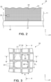
Fig. 2] Fig. 2 is an enlarged plan view of the wiring board according to the embodiment (enlarged view of part II inFig. 1 ). - [
Fig. 3] Fig. 3 is an enlarged plan view of the wiring board according to the embodiment (enlarged view of part III inFig. 2 ). - [
Fig. 4] Fig. 4 is a sectional view of the wiring board according to the embodiment (sectional view of line VI-VI inFig. 3 ). - [
Fig. 5] Fig. 5 is a sectional view of the wiring board according to the embodiment (sectional view of line V-V inFig. 3 ). - [
Fig. 6] Fig. 6 is a sectional view of a first-direction wiring line and a second-direction wiring line. - [
Fig. 7] Figs. 7A to 7E are sectional views illustrating a method for manufacturing the wiring board according to the embodiment. - [
Fig. 8] Figs. 8A to 8F are sectional views illustrating the method for manufacturing the wiring board according to the embodiment. - [
Fig. 9] Fig. 9 is a plan view of an image display device according to an embodiment. - An embodiment will be described with reference to
Figs. 1 to 9. Figs. 1 to 9 illustrate the present embodiment. - Drawings described below are schematic diagrams. Therefore, sizes and shapes of the components are exaggerated as appropriate to facilitate understanding. Changes are possible as appropriate without departing from the technical idea. In each of the drawings described below, the same parts are denoted by the same reference signs, and detailed description thereof may be omitted. The numerical values of, for example, the dimensions and the materials of components described in this specification are examples of the embodiment. The numerical values and materials are not limited to the examples, and may be selected as appropriate. In this specification, terms relating to shapes and geometric conditions, such as "parallel", "orthogonal", and "perpendicular", are to be interpreted not only in a strict sense but also to cover states that are substantially the same as those in a strict sense.
- In the embodiment described below, an "X direction" is a direction parallel to one side of a substrate. A "Y direction" is a direction perpendicular to the X direction and parallel to another side of the substrate. A "Z direction" is a direction perpendicular to both the X direction and the Y direction and parallel to a thickness direction of a wiring board. A "front surface" is a surface that faces in a positive Z direction and on which wiring lines are provided on the substrate. A "back surface" is a surface that faces in a negative Z direction and that is opposite to the surface on which the wiring lines are provided on the substrate.
- The structure of a wiring board according to the present embodiment will be described with reference to
Figs. 1 to 5. Figs. 1 to 5 illustrate the wiring board according to the present embodiment. - As illustrated in
Fig. 1 , awiring board 10 according to the present embodiment is disposed on, for example, a display of an image display device. Thewiring board 10 includes atransparent substrate 11 and mesh wiring layers (wiring pattern regions) 20 arranged on thesubstrate 11. The mesh wiring layers 20 are electrically connected to afeeding unit 40. - The
substrate 11 is substantially rectangular in plan view. The longitudinal direction of thesubstrate 11 is parallel to the Y direction, and the transverse direction of thesubstrate 11 is parallel to the X direction. Thesubstrate 11, which is transparent, is substantially flat plate-shaped, and has a substantially uniform thickness over the entirety thereof. A length L1 of thesubstrate 11 in the longitudinal direction (Y direction) may be selected from the range of, for example, 2 mm or more and 300 mm or less, preferably from the range of 100 mm or more and 200 mm or less. A length L2 of thesubstrate 11 in the transverse direction (X direction) may be selected from the range of, for example, 2 mm or more and 300 mm or less, preferably from the range of 50 mm or more and 100 mm or less. Thesubstrate 11 may have rounded corners. - The material of the
substrate 11 may be any material that is transparent in the visible light range and that has electrically insulating properties. The material of thesubstrate 11 is polyethylene terephthalate in the present embodiment, but is not limited to this. The material of thesubstrate 11 is preferably an organic insulating material, for example, a polyester-based resin such as polyethylene terephthalate, an acrylic resin such as polymethyl methacrylate, a polycarbonate-based resin, a polyimide-based resin, a polyolefin-based resin such as cycloolefin polymer, or a cellulose-based resin material such as triacetyl cellulose. Alternatively, the material of thesubstrate 11 may be an organic insulating material such as cycloolefin polymer (for example, ZF-16 produced by Zeon Corporation) or polynorbornene polymer (produced by Sumitomo Bakelite Co., Ltd.). The material of thesubstrate 11 may instead be glass, ceramic, etc., as appropriate depending on the use. Although thesubstrate 11 is composed of a single layer in the illustrated example, thesubstrate 11 is not limited to this, and may instead have a multilayer structure including a plurality of base materials or layers. Thesubstrate 11 may be film-shaped or plate-shaped. Thus, the thickness of thesubstrate 11 is not particularly limited, and may be selected as appropriate depending on the use. For example, a thickness (in the Z direction) T1 of the substrate 11 (seeFigs. 4 and 5 ) may be in the range of, for example, 5 µm or more and 200 µm or less. - The
substrate 11 may have a dielectric loss tangent of 0.002 or less, preferably 0.001 or less. The dielectric loss tangent of thesubstrate 11 has no particular lower limit, but may be more than 0. When the dielectric loss tangent of thesubstrate 11 is within the above-mentioned ranges, loss in gain (sensitivity) during transmission and reception of electromagnetic waves may be reduced, particularly in a case where high-frequency electromagnetic waves (for example, millimeter waves) are transmitted and received by the mesh wiring layers 20. The dielectric loss tangent of thesubstrate 11 has no particular lower limit. The dielectric constant of thesubstrate 11 is not particularly limited, and may instead be 2.0 or more and 10.0 or less. - The dielectric loss tangent of the
substrate 11 may be measured in accordance with IEC 62562. More specifically, first, a specimen is prepared by cutting out a portion of thesubstrate 11 on which no mesh wiring layers 20 are formed. Alternatively, a portion of thesubstrate 11 on which the mesh wiring layers 20 are formed may be cut out, and then the mesh wiring layers 20 may be removed by, for example, etching. The specimen has a width in the range of 10 mm to 20 mm and a length in the range of 50 mm to 100 mm. Next, the dielectric loss tangent is measured in accordance with IEC 62562. The dielectric constant and the dielectric loss tangent of thesubstrate 11 may also be measured in accordance with ASTM D150. - The transmittance of the
substrate 11 for visible light (light with a wavelength of 380 nm or more and 750 nm or less) may be 85% or more, preferably 90% or more. The transmittance of thesubstrate 11 for visible light has no particular upper limit, but may be, for example, 100% or less. When the transmittance of thesubstrate 11 for visible light is within the above-mentioned ranges, transparency of thewiring board 10 can be increased, and visibility of adisplay 91 of an image display device 90 (described below) can be enhanced. The visible light is light with a wavelength of 380 nm to 780 nm. The transmittance for visible light of 85% or more means that when the absorbance of thesubstrate 11 is measured with a known spectrophotometer (for example, spectrometer V-670 manufactured by JASCO Corporation), the transmittance is 85% or more over the entire wavelength range of 380 nm to 780 nm. - In the present embodiment, the mesh wiring layers 20 are composed of antenna pattern regions having a function of an antenna. In
Fig. 1 , the mesh wiring layers 20 (three in number), which are formed on thesubstrate 11, correspond to different frequency bands. More specifically, the mesh wiring layers 20 have different lengths (lengths in the Y direction) La, each of which corresponds to a specific frequency band. The mesh wiring layers 20 corresponding to frequency bands with lower frequencies have longer lengths La. When, for example, thewiring board 10 is disposed on adisplay 91 of an image display device 90 (seeFig. 9 described below), eachmesh wiring layer 20 may correspond to, for example, a telephone antenna, a WiFi antenna, a 3G antenna, a 4G antenna, a 5G antenna, an LTE antenna, a Bluetooth (registered trademark) antenna, or an NFC antenna. The mesh wiring layers 20 may be formed such that the mesh wiring layers 20 do not extend over the entire region of thesubstrate 11 but exist only in partial regions on thesubstrate 11. - Each
mesh wiring layer 20 is substantially rectangular in plan view. The longitudinal direction of eachmesh wiring layer 20 is parallel to the Y direction, and the transverse direction of eachmesh wiring layer 20 is parallel to the X direction. A length La of eachmesh wiring layer 20 in the longitudinal direction (Y direction) may be selected from the range of, for example, 1 mm or more and 100 mm or less. A width Wa of eachmesh wiring layer 20 in the transverse direction (X direction) may be selected from the range of, for example, 1 mm or more and 10 mm or less. The mesh wiring layers 20 may be millimeter wave antennas. When the mesh wiring layers 20 are millimeter wave antennas, the length La of eachmesh wiring layer 20 may be selected from the range of 1 mm or more and 10 mm or less, preferably 1.5 mm or more and 5 mm or less. - Each
mesh wiring layer 20 includes metal lines that form a grid structure or a mesh structure having a pattern periodic in the X direction and the Y direction. In other words, eachmesh wiring layer 20 has a pattern including portions extending in the X direction (second-direction wiring lines 22) and portions extending in the Y direction (first-direction wiring lines 21). - As illustrated in
Fig. 2 , eachmesh wiring layer 20 includes the first-direction wiring lines (antenna wiring lines) 21 that provide the function of an antenna and the second-direction wiring lines (antenna-connecting wiring lines) 22 that connect the first-direction wiring lines 21. More specifically, the first-direction wiring lines 21 and the second-direction wiring lines 22 are integrated together to form a grid structure or a mesh structure. Each first-direction wiring line 21 extends in a direction corresponding to the frequency band of the antenna (longitudinal direction, Y direction), and each second-direction wiring line 22 extends in a direction orthogonal to the first-direction wiring lines 21 (width direction, X direction). The first-direction wiring lines 21 have the length La corresponding to a predetermined frequency band (above-described length of themesh wiring layer 20, seeFig. 1 ) to mainly provide the function of an antenna. The second-direction wiring lines 22 connect the first-direction wiring lines 21 to each other to suppress defects such as breakage of the first-direction wiring lines 21 or electrical disconnection between each first-direction wiring line 21 and thefeeding unit 40. - As illustrated in
Fig. 3 , eachmesh wiring layer 20 has a plurality ofopenings 23 that are each surrounded by adjacent ones of the first-direction wiring lines 21 and adjacent ones of the second-direction wiring lines 22. The first-direction wiring lines 21 and the second-direction wiring lines 22 are arranged at equal intervals. More specifically, the first-direction wiring lines 21 are arranged at equal intervals, and a pitch P1 thereof may be in the range of, for example, 0.01 mm or more and 1 mm or less. The second-direction wiring lines 22 are arranged at equal intervals, and a pitch P2 thereof may be in the range of, for example, 0.01 mm or more and 1 mm or less. Since the first-direction wiring lines 21 and the second-direction wiring lines 22 are both arranged at equal intervals as described above, differences in size between theopenings 23 can be reduced in eachmesh wiring layer 20, so that themesh wiring layer 20 is not readily visible to the naked eye. The pitch P1 of the first-direction wiring lines 21 is equal to the pitch P2 of the second-direction wiring lines 22. Theopenings 23 are substantially square in plan view, and thesubstrate 11, which is transparent, is exposed at eachopening 23. Therefore, the overall transparency of thewiring board 10 can be increased by increasing the area of eachopening 23. A length L3 of each side of eachopening 23 may be in the range of, for example, 0.01 mm or more and 1 mm or less. Each first-direction wiring line 21 and each second-direction wiring line 22 are orthogonal to each other, but may instead cross each other at an acute or obtuse angle. Theopenings 23 preferably have the same shape and the same size over the entire region, but the shapes and sizes thereof may vary depending on the location and are not necessarily the same over the entire region. - As illustrated in
Fig. 4 , each first-direction wiring line 21 has a substantially rectangular or square cross section in a direction perpendicular to the longitudinal direction thereof (cross section in the X direction). The cross-sectional shape of each first-direction wiring line 21 is substantially uniform in the longitudinal direction of the first-direction wiring line 21 (Y direction). As illustrated inFig. 5 , each second-direction wiring line 22 has a substantially rectangular or square cross section in a direction perpendicular to the longitudinal direction thereof (cross section in the Y direction). The cross-sectional shape of each second-direction wiring line 22 is substantially the same as the above-described cross-sectional shape of each first-direction wiring line 21 (shape of cross section in the X direction). The cross-sectional shape of each second-direction wiring line 22 is substantially uniform in the longitudinal direction of the second-direction wiring line 22 (X direction). The cross-sectional shapes of each first-direction wiring line 21 and each second-direction wiring line 22 are not necessarily substantially rectangular or square, and may be, for example, a substantially trapezoidal shape that is narrower at the front side (side facing in the positive Z direction) than at the back side (side facing in the negative Z direction), or a shape having curved side surfaces at both ends in the longitudinal direction. - In the present embodiment, a line width W1 (dimension in the X direction, see
Fig. 4 ) of the first-direction wiring lines 21 and a line width W2 (dimension in the Y direction, seeFig. 5 ) of the second-direction wiring lines 22 are not particularly limited, and may be selected as appropriate depending on the use. For example, the line width W1 of the first-direction wiring lines 21 may be selected from the range of 0.1 µm or more and 5.0 µm or less. The line width W2 of the second-direction wiring lines 22 may be selected from the range of 0.1 µm or more and 5.0 µm or less. A height H1 (dimension in the Z direction, seeFig. 4 ) of the first-direction wiring lines 21 and a height H2 (dimension in the Z direction, seeFig. 5 ) of the second-direction wiring lines 22 are not particularly limited, and may be selected as appropriate depending on the use. For example, the heights H1 and H2 may be selected from the range of 0.1 µm or more and 5.0 µm or less. -
Fig. 6 illustrates a cross section of each of the first-direction wiring lines 21 and the second-direction wiring lines 22 taken in the width direction (X direction, Y direction). Each of the first-direction wiring lines 21 and the second-direction wiring lines 22 has afront surface 24a, aback surface 24b, and twoside surfaces front surface 24a is positioned at a side of the first-direction wiring lines 21 and the second-direction wiring lines 22 viewed by a viewer during use (side facing in the positive Z direction). Theback surface 24b is positioned opposite to thefront surface 24a at a side facing the substrate 11 (side facing in the negative Z direction). The twoside surfaces front surface 24a and theback surface 24b at both sides of each of the first-direction wiring lines 21 and the second-direction wiring lines 22 in the width direction (X direction, Y direction). In this case, thefront surface 24a is substantially orthogonal to the side surfaces 24c and 24d, and theback surface 24b is also substantially orthogonal to the side surfaces 24c and 24d. However, the surfaces are not limited to this, and may cross each other at an acute or obtuse angle. Thefront surface 24a, theback surface 24b, and the side surfaces 24c and 24d extend straight. However, thefront surface 24a, theback surface 24b, and the side surfaces 24c and 24d are not limited to this, and may instead be curved. - As illustrated in
Fig. 6 , each of the first-direction wiring lines 21 and the second-direction wiring lines 22 includes ametal layer 27 and a blackened layer (first layer) 28 disposed on themetal layer 27. Themetal layer 27 constitutes the main portion of each of the first-direction wiring lines 21 and the second-direction wiring lines 22, and is positioned at the center of each of the first-direction wiring lines 21 and the second-direction wiring lines 22. The blackenedlayer 28 is formed on the outer periphery of themetal layer 27, and defines the outermost surface of each of the first-direction wiring lines 21 and the second-direction wiring lines 22. - The material of the
metal layer 27 may be any conductive metal material. In the present embodiment, the material of themetal layer 27 is copper. However, the material is not limited to this. Examples of the material of themetal layer 27 include metal materials (including alloys), such as gold, silver, copper, platinum, tin, aluminum, iron, and nickel. - The blackened
layer 28 is formed to cover the outer surface of themetal layer 27. The blackenedlayer 28 is formed on themetal layer 27 at each of thefront surface 24a and the side surfaces 24c and 24d. The blackenedlayer 28 is preferably formed to extend over the entire regions of thefront surface 24a and the side surfaces 24c and 24d. The blackenedlayer 28 is not formed on themetal layer 27 at theback surface 24b. The overall color of the blackenedlayer 28 is black, and the blackenedlayer 28 reflects less visible light than themetal layer 27. The black color is not limited to achromatic black, and includes dark gray, chromatic black, and chromatic dark gray. - The material of the blackened
layer 28 is preferably a black metal material, and may contain, for example, palladium or tellurium. As described below, the palladium or tellurium may be provided by subjecting themetal layer 27 to a replacement process. More specifically, themetal layer 27 may be subjected to a replacement process in which metal atoms on the outer surface thereof are replaced with atoms of palladium or tellurium. Alternatively, as described below, the blackenedlayer 28 may be formed by subjecting themetal layer 27 to an oxidation process. More specifically, the outer surface of themetal layer 27 may be subjected to an oxidation process by using blackening liquid so that the blackenedlayer 28, which is an oxidized film obtained as a result of oxidation of themetal layer 27, is formed on the outer surface of themetal layer 27. In other words, the blackenedlayer 28 may contain an oxide of metal that forms themetal layer 27. When, for example, the material of themetal layer 27 is copper, the blackenedlayer 28 may contain copper oxide. - The blackened
layer 28 has a thickness T2 of 5 nm or more. The thickness T2 may be 10 nm or more, preferably 20 nm or more. When the thickness T2 of the blackenedlayer 28 is 5 nm or more, themetal layer 27 is sufficiently covered with the blackenedlayer 28, so that visible light can be sufficiently absorbed by the blackenedlayer 28. Accordingly, reflection of visible light by the blackenedlayer 28 can be suppressed so that themesh wiring layer 20 is not readily visible to the naked eye. In the present embodiment, visible light means light with a wavelength of 380 nm or more and 750 nm or less. - The thickness T2 of the blackened
layer 28 is 100 nm or less, preferably 60 nm or less. When the thickness T2 of the blackenedlayer 28 is 100 nm or less, reduction in conductivity of themesh wiring layer 20 due to the presence of the blackenedlayer 28 can be suppressed. Accordingly, reduction in current flow through themesh wiring layer 20 can be suppressed during transmission and reception of radio waves. - The thickness T2 of the blackened
layer 28 may be measured by the method of scanning transmission electron microscopy-energy dispersive X-ray spectroscopy (STEM-EDS). More specifically, the thickness T2 of the blackenedlayer 28 may be measured as follows. - First, before carrying out the STEM-EDS method, a test piece is subjected to preprocessing in which a cross section thereof is processed by a focus ion beam (FIB) method. In this case, before carrying out the FIB method, the test piece is subjected to preprocessing in which carbon is applied to the surface thereof to a thickness of 200 nm or more to form a protective film. The protective film may be made of, for example, Pt, PtPd, or Os instead of carbon. The protective film may be formed by, for example, sputtering or vapor deposition. The protective film suppresses damage to the surface of a portion processed in the process by the FIB method, and the thickness thereof may be adjusted as appropriate by adjusting processing conditions. An FIB device that is used may be any device as long as the device has a system capable of performing a process, such as microsampling, for picking up a sample from any location. For example, NB5000 manufactured by Hitachi High-Technologies Corporation may be used. The finishing thickness of a thin film formed on the cross section of the observed portion may be 50 nm to 150 nm.
- The STEM-EDS method is preferably carried out by an STEM-EDS device in which an acceleration voltage is 200 kV or more, which not only performs transmission electron microscope (TEM) observation but also includes an STEM system, and which is provided with a cold electron gun or a Schottky electron gun instead of a tungsten electron gun. For example, JEM-2100F manufactured by JEOL Ltd. may be used. When the blackened
layer 28 can be clearly observed by TEM observation, length measurement is performed on a TEM image. When the blackenedlayer 28 cannot be clearly observed by TEM observation, STEM-EDS is performed. When the blackenedlayer 28 contains palladium or tellurium, a region in which palladium or tellurium is present may be measured on a mapping image. When the blackenedlayer 28 contains copper oxide, a region in which oxygen is present may be measured on a mapping image. When the amount of detection is small, line scanning, for example, may be performed, and the location corresponding to the half-width may be determined as the interface. The thickness T2 of the blackenedlayer 28 is measured at a location separated from the ends of the cross section of the first-direction wiring lines 21 and the second-direction wiring lines 22 in the width direction thereof. For example, when the upper surface of one of the first-direction wiring lines 21 and the second-direction wiring lines 22 is measured, the measurement is performed at a location close to the center and separated from the ends in the width direction by a distance of 10% or more of the width of the first-direction wiring lines 21 and the second-direction wiring lines 22. When a side surface of one of the first-direction wiring lines 21 and the second-direction wiring lines 22 is measured, the measurement is performed at a location close to the center and separated from the ends in the thickness direction by a distance of 10% or more of the thickness of the first-direction wiring lines 21 and the second-direction wiring lines 22. The measurement may be performed at one location, but may also be performed at a certain number of locations, and the average of the measurement results may be calculated. - As illustrated in
Figs. 4 and 5 , an easilyadhesive layer 15 is formed on thesubstrate 11. The easilyadhesive layer 15, which increases adhesion between thesubstrate 11 and each of the first-direction wiring lines 21 and the second-direction wiring lines 22, is formed on the front surface of thesubstrate 11 over substantially the entire region thereof. The easilyadhesive layer 15 is composed of an insulating film. The material of the easilyadhesive layer 15 may be a colorless transparent resin, for example, an acrylic resin such as polymethyl (meth)acrylate, polyethyl (meth)acrylate, or a modified resin or copolymer thereof, a polyester, a polyvinyl resin such as polyvinyl alcohol, polyvinyl acetate, polyvinyl acetal, polyvinyl butyral, or a copolymer thereof, a polyurethane, an epoxy resin, a polyamide, or a chlorinated polyolefin. The thickness of the easilyadhesive layer 15 may be set as appropriate in the range of 10 nm or more and 800 nm or less. The easilyadhesive layer 15 may be formed on the front surface of thesubstrate 11 at least over eachmesh wiring layer 20. - An
adhesion enhancing layer 16 is formed on the easilyadhesive layer 15. Theadhesion enhancing layer 16 is located between the easilyadhesive layer 15 and each of the first-direction wiring lines 21 and the second-direction wiring lines 22. Theadhesion enhancing layer 16, which enhances the adhesion between thesubstrate 11 and each of the first-direction wiring lines 21 and the second-direction wiring lines 22, has the same shape as that of the first-direction wiring lines 21 and the second-direction wiring lines 22 in plan view. In other words, theadhesion enhancing layer 16 has a grid structure or a mesh structure in plan view. The material of theadhesion enhancing layer 16 may be, for example, titanium, titanium oxide, nickel, nickel oxide, or a metal oxide such as indium zinc oxide (IZO). The thickness of theadhesion enhancing layer 16 may be selected from the range of 10 nm or more and 100 nm or less. It is not necessary that theadhesion enhancing layer 16 be provided. - A
protective layer 17 is formed on the front surface of thesubstrate 11 so as to cover the first-direction wiring lines 21, the second-direction wiring lines 22, and the easilyadhesive layer 15. Theprotective layer 17, which protects the first-direction wiring lines 21 and the second-direction wiring lines 22, is formed on the front surface of thesubstrate 11 over substantially the entire region thereof. The material of theprotective layer 17 may be a colorless transparent insulating resin, for example, an acrylic resin such as polymethyl (meth)acrylate, polyethyl (meth)acrylate, or a modified resin or copolymer thereof, a polyester, a polyvinyl resin such as polyvinyl alcohol, polyvinyl acetate, polyvinyl acetal, polyvinyl butyral, or a copolymer thereof, a polyurethane, an epoxy resin, a polyamide, or a chlorinated polyolefin. The thickness of theprotective layer 17 may be selected from the range of 0.3 µm or more and 10 µm or less. Theprotective layer 17 may be formed on thesubstrate 11 to at least cover eachmesh wiring layer 20. - It is not necessary that all of the easily
adhesive layer 15, theadhesion enhancing layer 16, and theprotective layer 17 be provided. For example, the easilyadhesive layer 15 and theprotective layer 17 may be provided, and theadhesion enhancing layer 16 may be omitted. Alternatively, theadhesion enhancing layer 16 may be provided, and the easilyadhesive layer 15 and theprotective layer 17 may be omitted. - An overall opening ratio At of the
mesh wiring layer 20 may be in the range of, for example, 87% or more and less than 100%. When the overall opening ratio At of thewiring board 10 is in this range, thewiring board 10 may be sufficiently conductive and transparent. The opening ratio is a ratio (%) of the area of the opening region (region in which metal portions, such as the first-direction wiring lines 21 and the second-direction wiring lines 22, are not present and in which thesubstrate 11 is exposed) to the unit area in a predetermined region (for example, the entire region of the mesh wiring layer 20). - Referring to
Fig. 1 again, thefeeding unit 40 is electrically connected to the mesh wiring layers 20. Thefeeding unit 40 is composed of a substantially rectangular thin plate-shaped conductive member. The longitudinal direction of thefeeding unit 40 is parallel to the X direction, and the transverse direction of thefeeding unit 40 is parallel to the Y direction. Thefeeding unit 40 is disposed at an end of thesubstrate 11 in the longitudinal direction of the substrate 11 (end in the negative Y direction). Examples of the material of thefeeding unit 40 include metal materials (including alloys), such as gold, silver, copper, platinum, tin, aluminum, iron, and nickel. Thefeeding unit 40 is electrically connected to awireless communication circuit 92 of an image display device 90 (seeFig. 9 ) when thewiring board 10 is installed in theimage display device 90. Although thefeeding unit 40 is provided on the front surface of thesubstrate 11, thefeeding unit 40 is not limited to this, and a portion or the entirety thereof may instead be located outside the peripheral edge of thesubstrate 11. When thefeeding unit 40 is formed to be flexible, thefeeding unit 40 may be formed to extend to a side surface or a back surface of theimage display device 90 to provide electrical connection at the side surface or the back surface. - A method for manufacturing a wiring board according to the present embodiment will now be described with reference to
Figs. 7A to 7E andFigs. 8A to 8F .Figs. 7A to 7E andFigs. 8A to 8F are sectional views illustrating the method for manufacturing the wiring board according to the present embodiment. - First, as illustrated in
Fig. 7A , thesubstrate 11 is prepared, and the easilyadhesive layer 15 and theadhesion enhancing layer 16 are successively formed on the front surface of thesubstrate 11 over substantially the entire region thereof. The easilyadhesive layer 15 may be formed by, for example, roll coating, gravure coating, gravure reverse coating, micro gravure coating, slot die coating, die coating, knife coating, inkjet coating, dispenser coating, kiss coating, or spray coating. Theadhesion enhancing layer 16 may be formed by, for example, vapor deposition, sputtering, or plasma CVD. - Next, as illustrated in
Fig. 7B , aconductive layer 51 is formed on theadhesion enhancing layer 16 over substantially the entire region of the front surface of thesubstrate 11. In the present embodiment, the thickness of theconductive layer 51 is 200 nm. However, the thickness of theconductive layer 51 is not limited to this, and may be selected as appropriate from the range of 10 nm or more and 1000 nm or less. In the present embodiment, theconductive layer 51 is formed by sputtering by using copper. Theconductive layer 51 may instead be formed by, for example, plasma CVD. - Next, as illustrated in
Fig. 7C , a photocurable insulating resist 52 is applied to theconductive layer 51 over substantially the entire region of the front surface of thesubstrate 11. The photocurable insulating resist 52 may be, for example, an organic resin, such as an epoxy-based resin. - Subsequently, a
transparent imprinting mold 53 havingprojections 53a is prepared (seeFig. 7D ). Thismold 53 is brought closer to thesubstrate 11 so that the photocurable insulating resist 52 spreads between themold 53 and thesubstrate 11. Next, the photocurable insulating resist 52 is exposed to light through themold 53 to cure the photocurable insulating resist 52, so that an insulatinglayer 54 is formed. Thus,trenches 54a having shapes obtained by transferring the shapes of theprojections 53a are formed on the front surface of the insulatinglayer 54. Thetrenches 54a have a pattern corresponding to the first-direction wiring lines 21 and the second-direction wiring lines 22 in plan view. - After that, the
mold 53 is separated from the insulatinglayer 54, so that the insulatinglayer 54 having a cross-sectional structure illustrated inFig. 7E is obtained. The direction in which themold 53 is separated from the insulatinglayer 54 is preferably the Y direction in which the first-direction wiring lines 21, which are the longer wiring lines, extend. - Since the
trenches 54a are formed on the front surface of the insulatinglayer 54 by imprinting, thetrenches 54a can be formed in a fine shape. The method for forming the insulatinglayer 54 is not limited to this, and the insulatinglayer 54 may instead be formed by photolithography. In such a case, a resist pattern is formed by photolithography so that portions of theconductive layer 51 that correspond to the first-direction wiring lines 21 and the second-direction wiring lines 22 are exposed. - An insulating material may remain at the bottom of the
trenches 54a in the insulatinglayer 54. Therefore, the remaining insulating material is removed by a wet process using a permanganate solution or an organic solvent, such as N-Methyl-2-pyrrolidone, or a dry process using an oxygen plasma. - By removing the remaining insulating material as described above, the
trenches 54a at which theconductive layer 51 is exposed are formed as illustrated inFig. 8A . - Next, as illustrated in
Fig. 8B , thetrenches 54a in the insulatinglayer 54 are filled with aconductor 55. In the present embodiment, thetrenches 54a in the insulatinglayer 54 are filled with copper by electroplating by using theconductive layer 51 as a seed layer. - Next, as illustrated in
Fig. 8C , the insulatinglayer 54 is removed. The insulatinglayer 54 on thesubstrate 11 is removed by a wet process using a permanganate solution or an organic solvent, such as N-Methyl-2-pyrrolidone, or a dry process using an oxygen plasma. - Next, as illustrated in
Fig. 8D , theconductive layer 51 and theadhesion enhancing layer 16 on the front surface of thesubstrate 11 are removed. Theconductive layer 51 and theadhesion enhancing layer 16 are etched so that the front surface of thesubstrate 11 is exposed by a wet process using a copper etching solution, such as an aqueous solution of ferric chloride, an aqueous solution of cupric chloride, an aqueous solution of ammonium peroxodisulfate, an aqueous solution of sodium peroxodisulfate, sulfuric acid, or aqueous hydrogen peroxide. - Next, as illustrated in
Fig. 8E , the blackenedlayer 28 is formed on the outer periphery of the conductor 55 (metal layer 27) on the front surface of thesubstrate 11. The blackenedlayer 28 is formed so that the thickness T2 thereof is 5 nm or more and 100 nm or less. - In this case, the outer periphery of the
metal layer 27 may be subjected to a replacement process to form the blackenedlayer 28 containing palladium or tellurium. - The replacement process is a process in which metal atoms on the outer periphery of the
metal layer 27 are replaced with metal atoms of palladium or tellurium by utilizing the difference in ionization tendency between these metal atoms. Assuming, for example, that the material of themetal layer 27 is copper, which is a metal having a high ionization tendency, the copper is immersed in an aqueous solution containing metal ions of palladium or tellurium, which have a low ionization tendency. Accordingly, the copper dissolves into metal ions and releases electrons. The electrons reduce the palladium or tellurium so that the palladium or tellurium is deposited on themetal layer 27. - When the blackened
layer 28 contains palladium, the above-described aqueous solution preferably contains palladium at a concentration of 0.01 g/L or more and 10 g/L or less, and is preferably an acid solution containing nitric or sulfuric acid and chelate so that palladium is uniformly dissolved. When the blackenedlayer 28 contains tellurium, the above-described aqueous solution preferably contains tellurium at a concentration of 0.01 g/L or more and 10 g/L or less, and is preferably an acid solution containing nitric or sulfuric acid so that tellurium is uniformly dissolved. The thickness T2 of the blackenedlayer 28 can be adjusted to 5 nm or more and 100 nm or less by appropriately setting, for example, the time for which themetal layer 27 is immersed in the aqueous solution, the temperature of the aqueous solution, and the concentration of palladium or tellurium in the aqueous solution. - The blackened
layer 28 may instead be formed by subjecting the outer periphery of themetal layer 27 to an oxidation process. - The oxidation process is a process in which the outer periphery of the
metal layer 27 is oxidized to form a metal oxide on the outer periphery of themetal layer 27, so that the surface of themetal layer 27 is blackened. In this case, oxidizing liquid that is used may be, for example, a mixed aqueous solution of hypochlorite and sodium hydroxide, a mixed aqueous solution of chlorite and sodium hydroxide, or a mixed aqueous solution of peroxydisulfuric acid and sodium hydroxide. The thickness T2 of the blackenedlayer 28 can be adjusted to 5 nm or more and 100 nm or less by appropriately setting, for example, the time for which themetal layer 27 is immersed in the oxidizing liquid, the temperature of the oxidizing liquid, and concentrations of components of the oxidizing liquid. - After that, as illustrated in
Fig. 8F , theprotective layer 17 is formed to cover the easilyadhesive layer 15 and the blackenedlayer 28 on thesubstrate 11. Theprotective layer 17 may be formed by, for example, roll coating, gravure coating, gravure reverse coating, micro gravure coating, slot die coating, die coating, knife coating, inkjet coating, dispenser coating, kiss coating, spray coating, screen printing, offset printing, or flexographic printing. - Thus, the
wiring board 10 including thesubstrate 11 and the mesh wiring layers 20 arranged on thesubstrate 11 is obtained (Fig. 8E ). The mesh wiring layers 20 each include the first-direction wiring lines 21 and the second-direction wiring lines 22. Each of the first-direction wiring lines 21 and the second-direction wiring lines 22 includes themetal layer 27 and the blackenedlayer 28 formed on the outer periphery of themetal layer 27. Thefeeding unit 40 may be formed of a portion of theconductor 55. Alternatively, a flat plate-shapedfeeding unit 40 may be separately prepared, and the thus-prepared feeding unit 40 may be electrically connected to the mesh wiring layers 20. - The operations of the wiring board having the above-described structure will now be described.
- As illustrated in
Fig. 9 , thewiring board 10 is installed in theimage display device 90 having thedisplay 91. Thewiring board 10 is disposed on thedisplay 91. Theimage display device 90 may be, for example, a portable terminal device, such as a smartphone or a tablet. The mesh wiring layers 20 of thewiring board 10 are electrically connected to thewireless communication circuit 92 of theimage display device 90 through thefeeding unit 40. Thus, radio waves of predetermined frequencies can be transmitted and received through the mesh wiring layers 20. This enables communication using theimage display device 90. When theimage display device 90 includes a polarizing plate, thewiring board 10 is preferably disposed closer to the viewer than the polarizing plate. - As described above, according to the present embodiment, each of the first-
direction wiring lines 21 and the second-direction wiring lines 22 includes themetal layer 27 and the blackenedlayer 28 formed on the outer periphery of themetal layer 27, and the thickness T2 of the blackenedlayer 28 is 5 nm or more and 100 nm or less. Accordingly, the blackenedlayer 28 absorbs visible light, so that reflection of the visible light by themetal layer 27 can be suppressed. As a result, the visibility of the mesh wiring layers 20 on the front surface of thedisplay 91 can be reduced, so that the mesh wiring layers 20 are not readily visible to the naked eye of the viewer. Since the thickness T2 of the blackenedlayer 28 is as small as 100 nm or less, the resistance of the first-direction wiring lines 21 and the second-direction wiring lines 22 is not greatly increased due to the presence of the blackenedlayer 28. Accordingly, current flow through the first-direction wiring lines 21 and the second-direction wiring lines 22 can be facilitated during transmission and reception of radio waves. - In addition, in recent years, mobile terminal devices for fifth-generation (5G) communications have been developed. When the mesh wiring layers 20 of the
wiring board 10 are used as, for example, 5G antennas (in particular, millimeter wave antennas), the frequency of radio waves (millimeter waves) transmitted and received by the mesh wiring layers 20 is higher than that of radio waves transmitted and received by, for example, 4G antennas. In general, when an alternating current is applied to a wiring line, the current flow in a central region of the wiring line is reduced as the frequency is increased. Accordingly, the current flows along the surface of the wiring line. The phenomenon in which an alternating current applied to a wiring line flows only along the surface of the wiring line is referred to as the skin effect. A skin depth is the depth from the surface of the wiring line at which the current is reduced to 1/e (about 0.37) times the current along the surface of the wiring line at which the current most easily flows. In general, the skin depth δ can be determined by the following equation.

- In the above equation, ω is the angular frequency (= 2πf), µ is the permeability (4π × 10-7 [H/m] in vacuum), and σ is the conductivity of the conductor that forms the wiring lines (5.8 × 10⁷ [S/m] for copper). The skin depth δ of the wiring lines made of copper is about 2.3 µm when the frequency is 0.8 GHz, about 1.3 µm when the frequency is 2.4 GHz, about 1.0 µm when the frequency is 4.4 GHz, and about 0.85 µm when the frequency is 6 GHz. The frequency of radio waves (millimeter waves) transmitted and received by a 5G antenna (28 GHz to 39 GHz) is higher than the frequency of radio waves transmitted and received by, for example, a 4G antenna. When, for example, the frequency of the current is 28 GHz to 39 GHz, δ is about 0.3 µm to about 0.4 µm.
- In the present embodiment, the thickness T2 of the blackened
layer 28, which has a high electrical resistivity, is 100 nm or less. Thus, the thickness T2 of the blackenedlayer 28 is sufficiently smaller than the skin depth δ. Accordingly, the current flow through the mesh wiring layers 20 is not impeded by the blackenedlayer 28 having a high electrical resistivity. Conversely, since most of the portion through which the current easily flows is themetal layer 27, and the conductivity of this portion can be increased. When the mesh wiring layers 20 are used as antennas, the performance of the antennas can be maintained. In particular, when the mesh wiring layers 20 transmit and receive radio waves (millimeter waves), since the thickness T2 of the blackenedlayer 28 is 100 nm or less, the thickness T2 is sufficiently smaller than the skin depth δ of the copper wiring lines. Therefore, the current flow through the mesh wiring layers 20 is not impeded by the blackenedlayer 28. - In addition, in the present embodiment, the blackened
layer 28 may contain palladium or tellurium. Therefore, the conductivity of the blackenedlayer 28 is low, and the current flow through the mesh wiring layers 20 is not impeded. - In addition, in the present embodiment, the blackened
layer 28 may be formed by subjecting themetal layer 27 to an oxidation process. Accordingly, themetal layer 27 can be protected by the blackenedlayer 28, and rusting of themetal layer 27 can be suppressed. - In addition, according to the present embodiment, the dielectric loss tangent of the
substrate 11 is 0.002 or less. Accordingly, when high-frequency radio waves (millimeter waves) are transmitted and received by the mesh wiring layers 20, dielectric loss can be reduced during transmission and reception of the radio waves. - In addition, according to the present embodiment, since the easily
adhesive layer 15 is formed on thesubstrate 11, the adhesion between thesubstrate 11 and each of the first-direction wiring lines 21 and the second-direction wiring lines 22 can be increased. In addition, since theadhesion enhancing layer 16 is formed on the easilyadhesive layer 15, the adhesion between thesubstrate 11 and each of the first-direction wiring lines 21 and the second-direction wiring lines 22 can be further enhanced. - In addition, according to the present embodiment, the
protective layer 17 is formed on thesubstrate 11 so as to cover the first-direction wiring lines 21 and the second-direction wiring lines 22. Therefore, the first-direction wiring lines 21 and the second-direction wiring lines 22 can be protected from, for example, external impacts. - In addition, according to the present embodiment, each
mesh wiring layer 20 has a function of an antenna. Themesh wiring layer 20 that functions as an antenna can be disposed on the outermost surface of theimage display device 90. Therefore, the communication performance is higher than when an antenna is mounted in theimage display device 90. In addition, since a plurality of mesh wiring layers 20 that function as antennas can be arranged along the surface of theimage display device 90, the communication performance can be improved. - Although the mesh wiring layers 20 function as antennas in the example described in the present embodiment, the mesh wiring layers 20 are not limited to this. The mesh wiring layers 20 may instead have functions of, for example, hovering (function for enabling operation by the user without direct contact with a display), fingerprint authentication, heating, or noise filtering (shielding). Also in these cases, the visibility of the mesh wiring layers 20 can be reduced, and the current flow through the mesh wiring layers 20 can be facilitated.
- In addition, although the blackened
layer 28 is provided on both the first-direction wiring lines 21 and the second-direction wiring lines 22 in the example described in the present embodiment, the blackenedlayer 28 is not limited to this. The blackenedlayer 28 may instead be provided only on the first-direction wiring lines 21, or only on the second-direction wiring lines 22. Also, the blackenedlayer 28 may be provided on some of the first-direction wiring lines 21 and some of the second-direction wiring lines 22. - Examples of the present embodiment will now be described.
- Wiring boards according to Examples 1 to 3 and Comparative Example were prepared as described below.
- A copper mesh pattern was formed on a substrate composed of a PET film and having a thickness of 100 µm, and the mesh pattern was subjected to a blackening process. The blackening process was performed by immersing the copper mesh pattern on the substrate in an electroless palladium plating solution for a predetermined time. After that, the mesh pattern subjected to the blackening process was cleaned with ion-exchanged water and dried. Thus, a wiring board including a substrate and a mesh wiring layer including a blackened layer was obtained. The mesh wiring layer had a size of 3 mm in width and 24 mm in length. The mesh wiring layer was grid-shaped, and the line width of the wiring lines was 1 µm in both the width direction and the length direction of the mesh wiring layer. The height of the wiring lines was 1 µm, and the pitch of the wiring lines was 100 µm. A solid pattern made of copper (3 mm in width and 1 mm in length) was formed at each end of the mesh wiring layer in the length direction for resistance measurement. The thickness of the blackened layer was 15 nm.
- A wiring board of Example 2 was produced similarly to Example 1 except that the thickness of the blackened layer was 60 nm.
- A wiring board of Example 3 was produced similarly to Example 1 except that the thickness of the blackened layer was 8 nm.
- A wiring board of Comparative Example was produced similarly to Example 1 except that no blackened layer was formed.
- An L* value (color coordinate) and a resistance were measured for each of the wiring boards of Examples 1 to 3 and Comparative Example.
- The L* value (color coordinate) was measured by using a spectral colorimeter (CM-700d manufactured by Konica Minolta, Inc.). The wiring lines were too thin for direct measurement of the L* value (color coordinate). Therefore, a copper thin film (film thickness 1 µm) having a size of 1 cm square or more was formed on a substrate composed of a PET film and having a thickness of 100 µm by sputtering. The thus-formed copper thin film was subjected to a blackening process under the same conditions as those in Examples 1 to 3 and Comparative Example, and then measured. The measurement conditions of the color coordinate were as follows:
- Measurement Method: SCE method
- Viewing Angle: 10°
- Light Source: D65 light source
- A digital multimeter (CDM-2000D manufactured by Custom Corporation) was used to measure the resistance. The resistance between the solid patterns at both ends of the mesh wiring layer in the length direction was measured.
- The thickness of the blackened layer was measured by the above-described method of scanning transmission electron microscopy-energy dispersive X-ray spectroscopy (STEM-EDS).
- A wiring board with an L* value of 40 or less and a resistance less than or equal to a resistance that is 10% higher than that in Comparative Example (14.0 Ω) was rated "good (G)". The results are shown in Table 1.
[Table 1] Thickness of Blackened Layer L* Value (Color Coordinate) Resistance Overall Rating Example 1 15nm 39.1 14.5Ω G Example 2 60nm 17.2 15.2Ω G Example 3 8nm 39.8 14.4Ω G Comparative Example - 46.5 14.0Ω - - As shown in Table 1, each of the wiring boards according to Examples 1 to 3 had an L* value of 40 or less. Thus, reflection of visible light by the mesh wiring layer was suppressed. In addition, the mesh wiring layer of each of the wiring boards according to Examples 1 to 3 had a resistance that is not greatly higher than that of the mesh wiring layer of the wiring board according to Comparative Example.
- The components of the above-described embodiment and modifications may be applied in combination with each other as necessary. Also, some of the components of the above-described embodiment and modifications may be omitted.
Claims (20)
- A wiring board comprising:a substrate; anda mesh wiring layer disposed on the substrate and including a plurality of wiring lines,wherein the substrate has a transmittance of 85% or more for light with a wavelength of 380 nm or more and 750 nm or less,wherein each of the wiring lines includes a metal layer and a blackened layer disposed on the metal layer, andwherein the blackened layer has a thickness of 5 nm or more and 100 nm or less.
- The wiring board according to Claim 1, wherein the blackened layer comprises palladium or tellurium.
- The wiring board according to Claim 1, wherein the blackened layer is obtained by subjecting the metal layer to an oxidation process.
- The wiring board according to Claim 3, wherein the blackened layer comprises an oxide of a metal contained in the metal layer.
- The wiring board according to any one of Claims 1 to 4, wherein the mesh wiring layer is an antenna.
- The wiring board according to any one of Claims 1 to 5, wherein the metal layer comprises gold, silver, copper, platinum, tin, aluminum, iron, or nickel.
- The wiring board according to any one of Claims 1 to 6, wherein the substrate has a dielectric loss tangent of 0.002 or less.
- The wiring board according to any one of Claims 1 to 7, wherein the substrate has a thickness of 5 µm or more and 200 µm or less.
- The wiring board according to any one of Claims 1 to 8, wherein the substrate comprises cycloolefin polymer or polynorbornene polymer.
- The wiring board according to any one of Claims 1 to 9, wherein the mesh wiring layer is provided only on a portion of the substrate.
- A method for manufacturing a wiring board, the method comprising:a step of preparing a substrate; anda step of forming a mesh wiring layer including a plurality of wiring lines on the substrate,wherein the substrate has a transmittance of 85% or more for light with a wavelength of 380 nm or more and 750 nm or less,wherein each of the wiring lines includes a metal layer and a blackened layer disposed on the metal layer, andwherein the blackened layer has a thickness of 5 nm or more and 100 nm or less.
- The method for manufacturing a wiring board according to Claim 11, wherein the step of forming the mesh wiring layer includes a step of forming the metal layer and a step of forming the blackened layer on the metal layer, the blackened layer comprising palladium or tellurium.
- The method for manufacturing a wiring board according to Claim 11, wherein the step of forming the mesh wiring layer includes a step of forming the metal layer and a step of subjecting the metal layer to an oxidation process to form the blackened layer.
- The method for manufacturing a wiring board according to Claim 13, wherein the blackened layer comprises an oxide of a metal contained in the metal layer.
- The method for manufacturing a wiring board according to any one of Claims 11 to 14, wherein the mesh wiring layer is an antenna.
- The method for manufacturing a wiring board according to any one of Claims 11 to 15, wherein the metal layer comprises gold, silver, copper, platinum, tin, aluminum, iron, or nickel.
- The method for manufacturing a wiring board according to any one of Claims 11 to 16, wherein the substrate has a dielectric loss tangent of 0.002 or less.
- The method for manufacturing a wiring board according to any one of Claims 11 to 17, wherein the substrate has a thickness of 5 µm or more and 200 µm or less.
- The method for manufacturing a wiring board according to any one of Claims 11 to 18, wherein the substrate comprises cycloolefin polymer or polynorbornene polymer.
- The method for manufacturing a wiring board according to any one of Claims 11 to 19, wherein the mesh wiring layer is provided only on a portion of the substrate.
Applications Claiming Priority (2)
| Application Number | Priority Date | Filing Date | Title |
|---|---|---|---|
| JP2020070400 | 2020-04-09 | ||
| PCT/JP2021/015094 WO2021206177A1 (en) | 2020-04-09 | 2021-04-09 | Wiring board and method for manufacturing wiring board |
Publications (2)
| Publication Number | Publication Date |
|---|---|
| EP4135122A1 true EP4135122A1 (en) | 2023-02-15 |
| EP4135122A4 EP4135122A4 (en) | 2024-05-01 |
Family
ID=78022653
Family Applications (1)
| Application Number | Title | Priority Date | Filing Date |
|---|---|---|---|
| EP21784598.1A Pending EP4135122A4 (en) | 2020-04-09 | 2021-04-09 | PRINTED CIRCUIT BOARD AND METHOD FOR PRODUCING A PRINTED CIRCUIT BOARD |
Country Status (7)
| Country | Link |
|---|---|
| US (1) | US12424752B2 (en) |
| EP (1) | EP4135122A4 (en) |
| JP (1) | JPWO2021206177A1 (en) |
| KR (2) | KR102924187B1 (en) |
| CN (1) | CN115362600A (en) |
| TW (1) | TWI905166B (en) |
| WO (1) | WO2021206177A1 (en) |
Cited By (1)
| Publication number | Priority date | Publication date | Assignee | Title |
|---|---|---|---|---|
| EP4432464A4 (en) * | 2021-11-11 | 2025-08-13 | Lg Electronics Inc | TRANSPARENT ANTENNA MODULE AND METHOD FOR MANUFACTURING THE SAME |
Families Citing this family (2)
| Publication number | Priority date | Publication date | Assignee | Title |
|---|---|---|---|---|
| KR20230032084A (en) * | 2021-08-30 | 2023-03-07 | 동우 화인켐 주식회사 | Antenna device and image display device including the same |
| CN119998116A (en) * | 2022-11-18 | 2025-05-13 | Tdk株式会社 | Conductive film and display device |
Family Cites Families (21)
| Publication number | Priority date | Publication date | Assignee | Title |
|---|---|---|---|---|
| JP4339789B2 (en) * | 2002-08-08 | 2009-10-07 | 大日本印刷株式会社 | Electromagnetic wave shielding sheet and manufacturing method thereof |
| JP4620576B2 (en) | 2005-12-02 | 2011-01-26 | パナソニック株式会社 | Wireless device |
| JP5447813B2 (en) | 2009-09-16 | 2014-03-19 | 大日本印刷株式会社 | Transparent antenna |
| JP5636735B2 (en) | 2009-09-24 | 2014-12-10 | 大日本印刷株式会社 | Transparent antenna element and transparent antenna |
| US8570225B2 (en) | 2010-03-25 | 2013-10-29 | Sony Corporation | Antenna device and mobile device |
| JP6201623B2 (en) * | 2013-10-22 | 2017-09-27 | 大日本印刷株式会社 | Electrode member, method for manufacturing the same, touch panel using the electrode member, and image display device including the touch panel |
| JP2015103223A (en) * | 2013-11-28 | 2015-06-04 | グンゼ株式会社 | Conductive substrate, touch panel and electromagnetic wave shield |
| JP6233015B2 (en) * | 2013-12-26 | 2017-11-22 | 大日本印刷株式会社 | Electrode sheet, touch panel using the electrode sheet, and image display device provided with the touch panel |
| WO2015190484A1 (en) * | 2014-06-10 | 2015-12-17 | 富士フイルム株式会社 | Electrically-conductive laminate for touchscreen, touchscreen, and transparent electrically-conductive laminate |
| JP6421077B2 (en) | 2015-05-19 | 2018-11-07 | 富士フイルム株式会社 | Antenna manufacturing method and touch sensor |
| JP6528597B2 (en) * | 2015-08-20 | 2019-06-12 | 住友金属鉱山株式会社 | Conductive substrate, and method of manufacturing conductive substrate |
| JP6604552B2 (en) * | 2016-03-25 | 2019-11-13 | 大日本印刷株式会社 | antenna |
| JPWO2018047608A1 (en) * | 2016-09-08 | 2019-07-18 | 富士フイルム株式会社 | Method of manufacturing conductive film, conductive film, touch panel sensor, antenna, fingerprint recognition unit, and touch panel |
| JP7031663B2 (en) | 2017-04-17 | 2022-03-08 | 住友金属鉱山株式会社 | Conductive substrate |
| JP7172211B2 (en) * | 2017-07-28 | 2022-11-16 | Tdk株式会社 | Conductive substrates, electronic devices and display devices |
| WO2019065782A1 (en) | 2017-09-29 | 2019-04-04 | 富士フイルム株式会社 | Conductive film, touch panel sensor, touch panel, and method for producing conductive film |
| JP7035437B2 (en) * | 2017-10-11 | 2022-03-15 | 東レ株式会社 | Manufacturing method of substrate with conductive pattern and substrate with conductive pattern |
| TWI888871B (en) | 2017-11-29 | 2025-07-01 | 日商大日本印刷股份有限公司 | Manufacturing method of wiring board |
| CN111902570B (en) * | 2018-03-27 | 2022-11-08 | 三井金属矿业株式会社 | Surface-treated copper foil, copper-clad laminate, and method for producing printed wiring board |
| KR102194290B1 (en) * | 2018-07-23 | 2020-12-22 | 동우 화인켐 주식회사 | Antenna structure and display device including the same |
| WO2020184569A1 (en) * | 2019-03-12 | 2020-09-17 | 出光興産株式会社 | Circuit board and method for producing circuit board |
-
2021
- 2021-04-09 TW TW110112950A patent/TWI905166B/en active
- 2021-04-09 JP JP2022514138A patent/JPWO2021206177A1/ja active Pending
- 2021-04-09 KR KR1020227038546A patent/KR102924187B1/en active Active
- 2021-04-09 EP EP21784598.1A patent/EP4135122A4/en active Pending
- 2021-04-09 WO PCT/JP2021/015094 patent/WO2021206177A1/en not_active Ceased
- 2021-04-09 US US17/995,599 patent/US12424752B2/en active Active
- 2021-04-09 CN CN202180024780.1A patent/CN115362600A/en active Pending
- 2021-04-09 KR KR1020267003483A patent/KR20260020225A/en active Pending
Cited By (1)
| Publication number | Priority date | Publication date | Assignee | Title |
|---|---|---|---|---|
| EP4432464A4 (en) * | 2021-11-11 | 2025-08-13 | Lg Electronics Inc | TRANSPARENT ANTENNA MODULE AND METHOD FOR MANUFACTURING THE SAME |
Also Published As
| Publication number | Publication date |
|---|---|
| KR20260020225A (en) | 2026-02-10 |
| WO2021206177A1 (en) | 2021-10-14 |
| KR102924187B1 (en) | 2026-02-06 |
| TW202211536A (en) | 2022-03-16 |
| CN115362600A (en) | 2022-11-18 |
| JPWO2021206177A1 (en) | 2021-10-14 |
| US20230253708A1 (en) | 2023-08-10 |
| US12424752B2 (en) | 2025-09-23 |
| KR20220165752A (en) | 2022-12-15 |
| TWI905166B (en) | 2025-11-21 |
| EP4135122A4 (en) | 2024-05-01 |
Similar Documents
| Publication | Publication Date | Title |
|---|---|---|
| US20250016928A1 (en) | Wiring board and method for manufacturing wiring board | |
| EP3720256B1 (en) | Wiring board and method for manufacturing wiring board | |
| US12424752B2 (en) | Wiring board and method for manufacturing wiring board | |
| US11916285B2 (en) | Wiring board and method for manufacturing wiring board | |
| US9997822B2 (en) | Wireless communication device with an antenna adjacent to an edge of the device | |
| Lee et al. | Electrical characterization of highly efficient, optically transparent nanometers-thick unit cells for antenna-on-display applications | |
| US20230318203A1 (en) | Wiring board and method of manufacturing wiring board | |
| JP2022163867A (en) | Wiring board, module, wiring board manufacturing method, and module manufacturing method | |
| JP7859535B2 (en) | Wiring board and method for manufacturing a wiring board | |
| KR20240101613A (en) | Module, laminate for image display device, image display device, module manufacturing method, and wiring board | |
| JP7482390B2 (en) | Wiring board and method for manufacturing the same | |
| JP7593055B2 (en) | Wiring board and method for manufacturing the same | |
| EP4322330A1 (en) | Wiring board and method for manufacturing wiring board | |
| JP2022161299A (en) | Wiring board and image display device |
Legal Events
| Date | Code | Title | Description |
|---|---|---|---|
| STAA | Information on the status of an ep patent application or granted ep patent |
Free format text: STATUS: THE INTERNATIONAL PUBLICATION HAS BEEN MADE |
|
| PUAI | Public reference made under article 153(3) epc to a published international application that has entered the european phase |
Free format text: ORIGINAL CODE: 0009012 |
|
| STAA | Information on the status of an ep patent application or granted ep patent |
Free format text: STATUS: REQUEST FOR EXAMINATION WAS MADE |
|
| 17P | Request for examination filed |
Effective date: 20221103 |
|
| AK | Designated contracting states |
Kind code of ref document: A1 Designated state(s): AL AT BE BG CH CY CZ DE DK EE ES FI FR GB GR HR HU IE IS IT LI LT LU LV MC MK MT NL NO PL PT RO RS SE SI SK SM TR |
|
| DAV | Request for validation of the european patent (deleted) | ||
| DAX | Request for extension of the european patent (deleted) | ||
| REG | Reference to a national code |
Ref country code: DE Ref legal event code: R079 Free format text: PREVIOUS MAIN CLASS: H01P0011000000 Ipc: H01Q0005220000 |
|
| A4 | Supplementary search report drawn up and despatched |
Effective date: 20240404 |
|
| RIC1 | Information provided on ipc code assigned before grant |
Ipc: H05K 3/38 20060101ALN20240327BHEP Ipc: H05K 3/10 20060101ALN20240327BHEP Ipc: H05K 1/16 20060101ALN20240327BHEP Ipc: H01Q 1/40 20060101ALN20240327BHEP Ipc: H05K 3/24 20060101ALI20240327BHEP Ipc: H05K 1/09 20060101ALI20240327BHEP Ipc: H05K 1/02 20060101ALI20240327BHEP Ipc: H01Q 1/38 20060101ALI20240327BHEP Ipc: H01Q 5/22 20150101AFI20240327BHEP |
|
| STAA | Information on the status of an ep patent application or granted ep patent |
Free format text: STATUS: EXAMINATION IS IN PROGRESS |
|
| 17Q | First examination report despatched |
Effective date: 20260210 |