EP4132239A1 - Elektronische vorrichtung - Google Patents
Elektronische vorrichtung Download PDFInfo
- Publication number
- EP4132239A1 EP4132239A1 EP21778744.9A EP21778744A EP4132239A1 EP 4132239 A1 EP4132239 A1 EP 4132239A1 EP 21778744 A EP21778744 A EP 21778744A EP 4132239 A1 EP4132239 A1 EP 4132239A1
- Authority
- EP
- European Patent Office
- Prior art keywords
- camera
- electronic device
- hole
- reinforcing member
- display
- Prior art date
- Legal status (The legal status is an assumption and is not a legal conclusion. Google has not performed a legal analysis and makes no representation as to the accuracy of the status listed.)
- Granted
Links
Images

Classifications
-
- H—ELECTRICITY
- H05—ELECTRIC TECHNIQUES NOT OTHERWISE PROVIDED FOR
- H05K—PRINTED CIRCUITS; CASINGS OR CONSTRUCTIONAL DETAILS OF ELECTRIC APPARATUS; MANUFACTURE OF ASSEMBLAGES OF ELECTRICAL COMPONENTS
- H05K5/00—Casings, cabinets or drawers for electric apparatus
- H05K5/02—Details
- H05K5/0247—Electrical details of casings, e.g. terminals, passages for cables or wiring
-
- H—ELECTRICITY
- H04—ELECTRIC COMMUNICATION TECHNIQUE
- H04M—TELEPHONIC COMMUNICATION
- H04M1/00—Substation equipment, e.g. for use by subscribers
- H04M1/02—Constructional features of telephone sets
- H04M1/0202—Portable telephone sets, e.g. cordless phones, mobile phones or bar type handsets
- H04M1/026—Details of the structure or mounting of specific components
- H04M1/0264—Details of the structure or mounting of specific components for a camera module assembly
-
- H—ELECTRICITY
- H04—ELECTRIC COMMUNICATION TECHNIQUE
- H04N—PICTORIAL COMMUNICATION, e.g. TELEVISION
- H04N23/00—Cameras or camera modules comprising electronic image sensors; Control thereof
- H04N23/50—Constructional details
- H04N23/51—Housings
-
- H—ELECTRICITY
- H05—ELECTRIC TECHNIQUES NOT OTHERWISE PROVIDED FOR
- H05K—PRINTED CIRCUITS; CASINGS OR CONSTRUCTIONAL DETAILS OF ELECTRIC APPARATUS; MANUFACTURE OF ASSEMBLAGES OF ELECTRICAL COMPONENTS
- H05K5/00—Casings, cabinets or drawers for electric apparatus
- H05K5/0017—Casings, cabinets or drawers for electric apparatus with operator interface units
-
- H—ELECTRICITY
- H04—ELECTRIC COMMUNICATION TECHNIQUE
- H04M—TELEPHONIC COMMUNICATION
- H04M1/00—Substation equipment, e.g. for use by subscribers
- H04M1/02—Constructional features of telephone sets
- H04M1/0202—Portable telephone sets, e.g. cordless phones, mobile phones or bar type handsets
- H04M1/026—Details of the structure or mounting of specific components
- H04M1/0266—Details of the structure or mounting of specific components for a display module assembly
Definitions
- the present invention relates to the field of communication devices and technologies, and in particular, to an electronic device.
- the periscope camera is of a large volume and occupies a large space in the electronic device.
- a buffer space needs to be reserved, which results in a large thickness of the electronic device.
- an installation gap also needs to be reserved in the thickness direction. Consequently, the thickness of the electronic device cannot be further reduced.
- the present invention discloses an electronic device, to solve the problem of large thickness of existing electronic devices.
- the present invention adopts the following technical solutions:
- An electronic device includes a front housing, a rear housing, a display, a reinforcing member, and a camera.
- the front housing is provided with a first through hole.
- the rear housing is connected to the front housing.
- the display is installed on a housing.
- a mounting chamber is formed between the display, the front housing, and the rear housing.
- the reinforcing member is arranged in the mounting chamber.
- the reinforcing member is spaced apart from the display.
- the reinforcing member is connected to the rear housing.
- the reinforcing member is provided with a second through hole.
- the camera is installed in the mounting chamber.
- the camera is located between the display and the reinforcing member.
- the camera is installed in the first through hole.
- the camera includes a bracket, a chip, and a body connected successively.
- the bracket is connected to the front housing and the rear housing respectively.
- the chip is arranged corresponding to the second through hole.
- the first through hole is provided on the front housing, the camera is installed in the first through hole, the second through hole is provided on the reinforcing member, and the chip of the camera is arranged corresponding to the second through hole, so that the size of the electronic device in the thickness direction can be reduced, making the electronic device thinner.
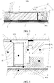
- a display 1 is installed on a front housing 2, a rear housing 5 is connected to the front housing 2, and the periscope camera is installed in a mounting chamber jointly defined by the front housing 2 and the rear housing 5.
- the periscope camera includes a body (including a lens and a motor) 31, a chip 32, a camera bracket 33.
- a reinforcing member 4 is arranged on the rear housing 5 at a position corresponding to the periscope camera.
- a buffer member 6 is arranged on an inner wall of the rear housing 5.
- the front housing 2 is provided with a wall thickness b at a bottom part of the periscope camera.
- the wall thickness b is generally 0.35 mm.
- the reinforcing member 4 covers above the periscope camera, and has a function of protecting the periscope camera from impact.
- a gap a is provided between the reinforcing member 4 and the periscope camera in order to avoid assembly interference.
- the gap a generally needs to be 0.25 mm.
- the periscope camera becomes a bottleneck in reducing the thickness of the entire device. As a result, the thickness of the electronic device is large and cannot be further reduced.
- an electronic device 100 includes a front housing 1, a rear housing 2, a display 3, a reinforcing member 4, and a camera 5.
- the front housing 1 is provided with a first through hole 001.
- the rear housing 2 is connected to the front housing 1.
- the display 3 is installed on a housing.
- a mounting chamber is formed between the display 3, the front housing 1, and the rear housing 2.
- the reinforcing member 4 is arranged in the mounting chamber.
- the reinforcing member 4 is spaced apart from the display 3.
- the reinforcing member 4 is connected to the rear housing 2.
- the reinforcing member 4 is provided with a second through hole 002.
- the camera 5 is installed in the mounting chamber.
- the camera 5 is located between the display 3 and the reinforcing member 4.
- the camera 5 is installed in the first through hole 001.
- the camera 5 includes a bracket 53, a chip 52, and a body 51 connected successively.
- the bracket 53 is connected to the front housing 1 and the rear housing 2 respectively.
- the chip 52 is arranged corresponding to the second through hole 002.
- the front housing 1 is provided with the first through hole 001, and the camera 5 is installed in the first through hole 001, the wall thickness b of the front housing 1 at this position in the related art can be reduced, and the wall thickness may even be reduced to zero, so that the thickness of the electronic device 100 can be reduced by 0.3 mm approximately.
- the reinforcing member 4 is provided with the second through hole 002, and the chip 52 of the camera 5 is arranged corresponding to the second through hole 002, the second through hole 002 can be used to reserve the installation gap for the chip 52 to avoid interference, thereby reducing the gap a between the camera 5 and the reinforcing member 4 in the related art. In this way, not only the reliability of the electronic device 100 can be ensured, but also the bottleneck in reducing the thickness can be overcome, and the size of electronic device 100 in the thickness direction is reduced, making the electronic device 100 thinner.
- the first through hole 001 is provided on the front housing 1 (that is, a portion of the front housing 1 corresponding to the camera 5 is hollowed)
- the camera 5 is installed in the first through hole 001
- the second through hole 002 is provided on the reinforcing member 4
- the chip 52 of the camera 5 is arranged corresponding to the second through hole 002
- the size of the electronic device 100 in the thickness direction can be reduced, making the electronic device 100 thinner.
- a peripheral surface of the camera 5 matches with an inner wall surface of the first through hole 001, and a front surface of the camera 5 abuts against the display 3. Therefore, the wall thickness b of the front housing 1 of the camera 5 in the related art can be reduced to zero.
- a first buffer member 7 is arranged in the first through hole 001, and the first buffer member 7 is connected to the front surface of the camera 5 and the display 3.
- the first buffer member 7 may be arranged between the camera 5 and the display 3, to protect the display 3 when the electronic device 100 is under an external force, thereby reducing the probability of cracking of the display 3 and improving the reliability.
- a thickness n of the first buffer member 7 satisfies: n ⁇ 0.25 mm. That is, a gap of no more than 0.25 mm is reserved between the front surface of the camera 5 and the display 3 for installing a buffer member.
- the thickness of the first buffer member 7 may be 0.1 mm, 0.2 mm, etc.
- the thickness of the first buffer member 7 may also have other values, and may be set as required according to the reliability of the display 3, which is not particularly limited in the present invention. It can be understood that, compared with the arrangement in the related art shown in FIG. 1 and FIG. 2 . the arrangement of the first buffer member 7 in the embodiments of the present invention can still satisfy the requirement of reducing the thickness of the electronic device 100.
- an area of the second through hole 002 is larger than an area of an orthographic projection of the chip 52 on the reinforcing member 4.
- the chip 52 of the camera 5 can be completely accommodated in the position corresponding to the second through hole 002.
- the second through hole 002 can completely accommodate the assembly tolerance between the chip 52 of the camera 5 and the body 51, and the second through hole 002 can also be used to reserve a gap for the chip 52 to prevent interference, so that the gap a in the related art can be reduced, or even the gap a can be eliminated to further reduce the thickness of the electronic device 100.
- the electronic device 100 further includes: a back cover 6.
- the back cover 6 is connected to the rear housing 2.
- the mounting chamber is closed by the back cover 6.
- the reinforcing member 4 is connected between the back cover 6 and the rear housing 2.
- the back cover 6 can provide protection for the camera 5 and other components.
- the reinforcing member 4 can cooperate with the back cover 6 to improve the stability and reliability of the camera 5.
- the chip 52 is spaced apart from the back cover 6. It can be understood that, the arrangement of the second through hole 002 can space the chip 52 apart from the back cover 6 to prevent the chip 52 from directly abutting against the back cover 6, and prevent the chip 52 from being squeezed when the back cover 6 is under an external force, thereby further improving the reliability.
- a distance m between the chip 52 and an inner surface of the back cover 6 satisfies: 0.08 mm ⁇ m ⁇ 0.12 mm.
- a distance of 0.08 mm to 0.12 mm, for example, 0.08 mm, 0.1 mm, or 0.11 mm is provided between the chip 52 of the camera 5 and the back cover 6.
- the distance can prevent the chip 52 and the back cover 6 from interfering with each other, thereby facilitating assembly.
- the existence of the distance can also buffer certain pressure to reduce the probability of damage to the chip 52.
- a second buffer member 8 is arranged between the back cover 6 and the rear housing 2, the second buffer member 8 is connected to an inner surface of the back cover 6 and a rear surface of the rear housing 2, and the second buffer member 8 is provided with a third through hole 003 for avoiding the camera 5.
- the back cover 6 and the rear housing 2 can be elastically connected by the second buffer member 8, and the arrangement of the first through hole 003 allows for receiving the camera 5 therein, to prevent the accumulation of the second buffer member 8 and the camera 5 in the thickness direction, which can improve the reliability while helping reduce the thickness, achieving a more compact and reasonable structural layout in the electronic device 100.
- the first buffer member 7 may be a foam or silica gel
- the second buffer member 8 may also be a foam or silica gel.
- the first buffer member 7 and the second buffer member 8 can provide a buffer effect for the camera 5 through elastic deformation and improve the reliability of the camera 5 and the display 3 under an external force or impact, and are easy to assemble and cost-effective.
- the reinforcing member 4 is a steel sheet, and a rear surface of the camera 5 is connected to the reinforcing member 4. In this way, the reinforcing member 4 can provide certain protection for the camera 5, thereby improving the stability and reliability of the electronic device.
- the electronic device 100 can effectively reduce the size of the electronic device 100 in the thickness direction, making the electronic device 100 thinner.
Landscapes
- Engineering & Computer Science (AREA)
- Signal Processing (AREA)
- Microelectronics & Electronic Packaging (AREA)
- Multimedia (AREA)
- Studio Devices (AREA)
- Camera Bodies And Camera Details Or Accessories (AREA)
Applications Claiming Priority (2)
| Application Number | Priority Date | Filing Date | Title |
|---|---|---|---|
| CN202010238576.7A CN111405791B (zh) | 2020-03-30 | 2020-03-30 | 电子设备 |
| PCT/CN2021/083908 WO2021197313A1 (zh) | 2020-03-30 | 2021-03-30 | 电子设备 |
Publications (3)
| Publication Number | Publication Date |
|---|---|
| EP4132239A1 true EP4132239A1 (de) | 2023-02-08 |
| EP4132239A4 EP4132239A4 (de) | 2023-10-04 |
| EP4132239B1 EP4132239B1 (de) | 2024-09-04 |
Family
ID=71437121
Family Applications (1)
| Application Number | Title | Priority Date | Filing Date |
|---|---|---|---|
| EP21778744.9A Active EP4132239B1 (de) | 2020-03-30 | 2021-03-30 | Elektronische vorrichtung |
Country Status (5)
| Country | Link |
|---|---|
| US (1) | US12355906B2 (de) |
| EP (1) | EP4132239B1 (de) |
| CN (1) | CN111405791B (de) |
| ES (1) | ES2990000T3 (de) |
| WO (1) | WO2021197313A1 (de) |
Families Citing this family (1)
| Publication number | Priority date | Publication date | Assignee | Title |
|---|---|---|---|---|
| CN111405791B (zh) | 2020-03-30 | 2021-05-18 | 维沃移动通信有限公司 | 电子设备 |
Family Cites Families (24)
| Publication number | Priority date | Publication date | Assignee | Title |
|---|---|---|---|---|
| JP3929320B2 (ja) * | 2002-02-06 | 2007-06-13 | 京セラ株式会社 | 小形モジュールカメラ |
| KR100891330B1 (ko) * | 2007-02-21 | 2009-03-31 | 삼성전자주식회사 | 반도체 패키지 장치와, 반도체 패키지의 제조방법과,반도체 패키지 장치를 갖는 카드 장치 및 반도체 패키지장치를 갖는 카드 장치의 제조 방법 |
| TW201205141A (en) * | 2010-07-16 | 2012-02-01 | Hon Hai Prec Ind Co Ltd | Image capturing device |
| CN204795931U (zh) * | 2015-07-09 | 2015-11-18 | 上海与德通讯技术有限公司 | 一种后摄像头的装饰模组及电子设备 |
| KR20170035237A (ko) * | 2015-09-22 | 2017-03-30 | 엘지전자 주식회사 | 이동 단말기 및 그 제어방법 |
| US10256527B2 (en) * | 2016-01-11 | 2019-04-09 | Lg Electronics Inc. | Mobile terminal |
| US20190148429A1 (en) * | 2016-03-12 | 2019-05-16 | Ningbo Sunny Opotech Co., Ltd. | Camera module, and photosensitive component thereof and manufacturing method therefor |
| CN206686225U (zh) * | 2017-02-13 | 2017-11-28 | 惠州Tcl移动通信有限公司 | 终端壳体组件及移动终端 |
| CN207039674U (zh) * | 2017-08-09 | 2018-02-23 | 维沃移动通信有限公司 | 一种移动终端 |
| CN109698894B (zh) * | 2017-10-20 | 2023-06-30 | 宁波舜宇光电信息有限公司 | 基于金属支架的感光组件和摄像模组 |
| CN107888729A (zh) * | 2017-11-30 | 2018-04-06 | 广东欧珀移动通信有限公司 | 支架组件、摄像头及电子设备 |
| KR102443229B1 (ko) * | 2018-01-23 | 2022-09-15 | 삼성전자주식회사 | 센서를 장착하기 위한 개구를 포함하는 디스플레이 |
| US10917506B2 (en) * | 2018-02-05 | 2021-02-09 | Guangdong Oppo Mobile Telecommunications Corp., Ltd. | Terminal display assembly and mobile terminal |
| WO2019164310A1 (en) * | 2018-02-21 | 2019-08-29 | Samsung Electronics Co., Ltd. | Electronic device including shield member for shielding at least part of magnetic force generated by magnetic substance and connection portion including property of nonmagnetic substance connected to shield member |
| US10277786B1 (en) * | 2018-02-23 | 2019-04-30 | Veoneer Us, Inc. | Camera module assembly for a motor vehicle |
| CN207802155U (zh) * | 2018-03-14 | 2018-08-31 | 欧菲影像技术(广州)有限公司 | 抗电磁干扰的摄像模组 |
| CN110460697B (zh) * | 2018-05-07 | 2021-07-13 | Oppo广东移动通信有限公司 | 电子设备 |
| CN208386733U (zh) * | 2018-06-14 | 2019-01-15 | Oppo广东移动通信有限公司 | 摄像头组件及应用该摄像头组件的电子装置 |
| CN108521542A (zh) * | 2018-06-15 | 2018-09-11 | 深圳超多维科技有限公司 | 一种电子设备的后摄像头支撑架及具有其的电子设备 |
| CN108957819A (zh) * | 2018-07-09 | 2018-12-07 | Oppo广东移动通信有限公司 | 电子装置 |
| CN208836246U (zh) * | 2018-09-11 | 2019-05-07 | Oppo(重庆)智能科技有限公司 | 电子设备 |
| CN209233925U (zh) * | 2018-12-28 | 2019-08-09 | 深圳传音通讯有限公司 | 摄像头安装结构及终端设备 |
| CN210075377U (zh) * | 2019-06-22 | 2020-02-14 | 王之奇 | 一种摄像头封装模组 |
| CN111405791B (zh) * | 2020-03-30 | 2021-05-18 | 维沃移动通信有限公司 | 电子设备 |
-
2020
- 2020-03-30 CN CN202010238576.7A patent/CN111405791B/zh active Active
-
2021
- 2021-03-30 EP EP21778744.9A patent/EP4132239B1/de active Active
- 2021-03-30 WO PCT/CN2021/083908 patent/WO2021197313A1/zh not_active Ceased
- 2021-03-30 ES ES21778744T patent/ES2990000T3/es active Active
-
2022
- 2022-09-27 US US17/954,312 patent/US12355906B2/en active Active
Also Published As
| Publication number | Publication date |
|---|---|
| US20230017831A1 (en) | 2023-01-19 |
| US12355906B2 (en) | 2025-07-08 |
| WO2021197313A1 (zh) | 2021-10-07 |
| EP4132239A4 (de) | 2023-10-04 |
| CN111405791B (zh) | 2021-05-18 |
| EP4132239B1 (de) | 2024-09-04 |
| CN111405791A (zh) | 2020-07-10 |
| ES2990000T3 (es) | 2024-11-28 |
Similar Documents
| Publication | Publication Date | Title |
|---|---|---|
| JP7457147B2 (ja) | 電子機器 | |
| US12316794B2 (en) | Electronic device | |
| KR102044471B1 (ko) | 변형 방지를 위한 프레임 조립 구조 및 이것을 갖는 전자 장치 | |
| US6309037B2 (en) | PCI I/O bracket retainer | |
| CN209448765U (zh) | 终端设备 | |
| US12355906B2 (en) | Electronic device | |
| CN110113460B (zh) | 电子设备 | |
| EP4207723B1 (de) | Elektronische vorrichtung | |
| JP6561705B2 (ja) | 情報処理装置 | |
| CN112462862B (zh) | 用于扩充卡槽口的电磁遮蔽结构及其扩充卡挡板 | |
| CN210157271U (zh) | 用于遮挡摄像头的挡门结构和电子设备 | |
| JP6083317B2 (ja) | シールドケースおよび電子機器 | |
| CN112201153B (zh) | 电子设备及其生产工艺 | |
| CN117677042A (zh) | 一种板卡结构 | |
| JP2008193630A (ja) | スライド式小型電子機器 | |
| TWI919337B (zh) | 顯示裝置及其組裝方法 | |
| KR100622895B1 (ko) | 이동통신 단말기의 엘씨디 고정구조 | |
| CN223024533U (zh) | 电子设备 | |
| CN213027327U (zh) | 一种体积小巧的接线箱 | |
| CN115000674B (zh) | 一种电子设备 | |
| CN102761014A (zh) | 连接器安装装置 | |
| CN217485376U (zh) | 防触电断路器 | |
| TW202605474A (zh) | 顯示裝置及其組裝方法 | |
| EP3291517B1 (de) | Anzeigebildschirmanordnung und mobiles endgerät | |
| CN120143941A (zh) | 一种台式机机箱 |
Legal Events
| Date | Code | Title | Description |
|---|---|---|---|
| STAA | Information on the status of an ep patent application or granted ep patent |
Free format text: STATUS: THE INTERNATIONAL PUBLICATION HAS BEEN MADE |
|
| PUAI | Public reference made under article 153(3) epc to a published international application that has entered the european phase |
Free format text: ORIGINAL CODE: 0009012 |
|
| STAA | Information on the status of an ep patent application or granted ep patent |
Free format text: STATUS: REQUEST FOR EXAMINATION WAS MADE |
|
| 17P | Request for examination filed |
Effective date: 20221024 |
|
| AK | Designated contracting states |
Kind code of ref document: A1 Designated state(s): AL AT BE BG CH CY CZ DE DK EE ES FI FR GB GR HR HU IE IS IT LI LT LU LV MC MK MT NL NO PL PT RO RS SE SI SK SM TR |
|
| DAV | Request for validation of the european patent (deleted) | ||
| DAX | Request for extension of the european patent (deleted) | ||
| A4 | Supplementary search report drawn up and despatched |
Effective date: 20230831 |
|
| RIC1 | Information provided on ipc code assigned before grant |
Ipc: H04M 1/02 20060101ALI20230825BHEP Ipc: H04N 23/51 20230101ALI20230825BHEP Ipc: H05K 5/02 20060101AFI20230825BHEP |
|
| GRAP | Despatch of communication of intention to grant a patent |
Free format text: ORIGINAL CODE: EPIDOSNIGR1 |
|
| STAA | Information on the status of an ep patent application or granted ep patent |
Free format text: STATUS: GRANT OF PATENT IS INTENDED |
|
| INTG | Intention to grant announced |
Effective date: 20240423 |
|
| GRAS | Grant fee paid |
Free format text: ORIGINAL CODE: EPIDOSNIGR3 |
|
| GRAA | (expected) grant |
Free format text: ORIGINAL CODE: 0009210 |
|
| STAA | Information on the status of an ep patent application or granted ep patent |
Free format text: STATUS: THE PATENT HAS BEEN GRANTED |
|
| AK | Designated contracting states |
Kind code of ref document: B1 Designated state(s): AL AT BE BG CH CY CZ DE DK EE ES FI FR GB GR HR HU IE IS IT LI LT LU LV MC MK MT NL NO PL PT RO RS SE SI SK SM TR |
|
| REG | Reference to a national code |
Ref country code: GB Ref legal event code: FG4D |
|
| REG | Reference to a national code |
Ref country code: CH Ref legal event code: EP |
|
| REG | Reference to a national code |
Ref country code: IE Ref legal event code: FG4D |
|
| REG | Reference to a national code |
Ref country code: DE Ref legal event code: R096 Ref document number: 602021018418 Country of ref document: DE |
|
| REG | Reference to a national code |
Ref country code: NL Ref legal event code: FP |
|
| REG | Reference to a national code |
Ref country code: ES Ref legal event code: FG2A Ref document number: 2990000 Country of ref document: ES Kind code of ref document: T3 Effective date: 20241128 |
|
| REG | Reference to a national code |
Ref country code: LT Ref legal event code: MG9D |
|
| PG25 | Lapsed in a contracting state [announced via postgrant information from national office to epo] |
Ref country code: NO Free format text: LAPSE BECAUSE OF FAILURE TO SUBMIT A TRANSLATION OF THE DESCRIPTION OR TO PAY THE FEE WITHIN THE PRESCRIBED TIME-LIMIT Effective date: 20241204 |
|
| PG25 | Lapsed in a contracting state [announced via postgrant information from national office to epo] |
Ref country code: PL Free format text: LAPSE BECAUSE OF FAILURE TO SUBMIT A TRANSLATION OF THE DESCRIPTION OR TO PAY THE FEE WITHIN THE PRESCRIBED TIME-LIMIT Effective date: 20240904 Ref country code: GR Free format text: LAPSE BECAUSE OF FAILURE TO SUBMIT A TRANSLATION OF THE DESCRIPTION OR TO PAY THE FEE WITHIN THE PRESCRIBED TIME-LIMIT Effective date: 20241205 Ref country code: FI Free format text: LAPSE BECAUSE OF FAILURE TO SUBMIT A TRANSLATION OF THE DESCRIPTION OR TO PAY THE FEE WITHIN THE PRESCRIBED TIME-LIMIT Effective date: 20240904 |
|
| PG25 | Lapsed in a contracting state [announced via postgrant information from national office to epo] |
Ref country code: BG Free format text: LAPSE BECAUSE OF FAILURE TO SUBMIT A TRANSLATION OF THE DESCRIPTION OR TO PAY THE FEE WITHIN THE PRESCRIBED TIME-LIMIT Effective date: 20240904 |
|
| PG25 | Lapsed in a contracting state [announced via postgrant information from national office to epo] |
Ref country code: LV Free format text: LAPSE BECAUSE OF FAILURE TO SUBMIT A TRANSLATION OF THE DESCRIPTION OR TO PAY THE FEE WITHIN THE PRESCRIBED TIME-LIMIT Effective date: 20240904 |
|
| PG25 | Lapsed in a contracting state [announced via postgrant information from national office to epo] |
Ref country code: HR Free format text: LAPSE BECAUSE OF FAILURE TO SUBMIT A TRANSLATION OF THE DESCRIPTION OR TO PAY THE FEE WITHIN THE PRESCRIBED TIME-LIMIT Effective date: 20240904 |
|
| PG25 | Lapsed in a contracting state [announced via postgrant information from national office to epo] |
Ref country code: RS Free format text: LAPSE BECAUSE OF FAILURE TO SUBMIT A TRANSLATION OF THE DESCRIPTION OR TO PAY THE FEE WITHIN THE PRESCRIBED TIME-LIMIT Effective date: 20241204 |
|
| PG25 | Lapsed in a contracting state [announced via postgrant information from national office to epo] |
Ref country code: RS Free format text: LAPSE BECAUSE OF FAILURE TO SUBMIT A TRANSLATION OF THE DESCRIPTION OR TO PAY THE FEE WITHIN THE PRESCRIBED TIME-LIMIT Effective date: 20241204 Ref country code: PL Free format text: LAPSE BECAUSE OF FAILURE TO SUBMIT A TRANSLATION OF THE DESCRIPTION OR TO PAY THE FEE WITHIN THE PRESCRIBED TIME-LIMIT Effective date: 20240904 Ref country code: NO Free format text: LAPSE BECAUSE OF FAILURE TO SUBMIT A TRANSLATION OF THE DESCRIPTION OR TO PAY THE FEE WITHIN THE PRESCRIBED TIME-LIMIT Effective date: 20241204 Ref country code: LV Free format text: LAPSE BECAUSE OF FAILURE TO SUBMIT A TRANSLATION OF THE DESCRIPTION OR TO PAY THE FEE WITHIN THE PRESCRIBED TIME-LIMIT Effective date: 20240904 Ref country code: HR Free format text: LAPSE BECAUSE OF FAILURE TO SUBMIT A TRANSLATION OF THE DESCRIPTION OR TO PAY THE FEE WITHIN THE PRESCRIBED TIME-LIMIT Effective date: 20240904 Ref country code: GR Free format text: LAPSE BECAUSE OF FAILURE TO SUBMIT A TRANSLATION OF THE DESCRIPTION OR TO PAY THE FEE WITHIN THE PRESCRIBED TIME-LIMIT Effective date: 20241205 Ref country code: FI Free format text: LAPSE BECAUSE OF FAILURE TO SUBMIT A TRANSLATION OF THE DESCRIPTION OR TO PAY THE FEE WITHIN THE PRESCRIBED TIME-LIMIT Effective date: 20240904 Ref country code: BG Free format text: LAPSE BECAUSE OF FAILURE TO SUBMIT A TRANSLATION OF THE DESCRIPTION OR TO PAY THE FEE WITHIN THE PRESCRIBED TIME-LIMIT Effective date: 20240904 |
|
| REG | Reference to a national code |
Ref country code: AT Ref legal event code: MK05 Ref document number: 1721771 Country of ref document: AT Kind code of ref document: T Effective date: 20240904 |
|
| PG25 | Lapsed in a contracting state [announced via postgrant information from national office to epo] |
Ref country code: IS Free format text: LAPSE BECAUSE OF FAILURE TO SUBMIT A TRANSLATION OF THE DESCRIPTION OR TO PAY THE FEE WITHIN THE PRESCRIBED TIME-LIMIT Effective date: 20250104 Ref country code: PT Free format text: LAPSE BECAUSE OF FAILURE TO SUBMIT A TRANSLATION OF THE DESCRIPTION OR TO PAY THE FEE WITHIN THE PRESCRIBED TIME-LIMIT Effective date: 20250106 |
|
| PG25 | Lapsed in a contracting state [announced via postgrant information from national office to epo] |
Ref country code: SM Free format text: LAPSE BECAUSE OF FAILURE TO SUBMIT A TRANSLATION OF THE DESCRIPTION OR TO PAY THE FEE WITHIN THE PRESCRIBED TIME-LIMIT Effective date: 20240904 Ref country code: RO Free format text: LAPSE BECAUSE OF FAILURE TO SUBMIT A TRANSLATION OF THE DESCRIPTION OR TO PAY THE FEE WITHIN THE PRESCRIBED TIME-LIMIT Effective date: 20240904 |
|
| PG25 | Lapsed in a contracting state [announced via postgrant information from national office to epo] |
Ref country code: AT Free format text: LAPSE BECAUSE OF FAILURE TO SUBMIT A TRANSLATION OF THE DESCRIPTION OR TO PAY THE FEE WITHIN THE PRESCRIBED TIME-LIMIT Effective date: 20240904 Ref country code: EE Free format text: LAPSE BECAUSE OF FAILURE TO SUBMIT A TRANSLATION OF THE DESCRIPTION OR TO PAY THE FEE WITHIN THE PRESCRIBED TIME-LIMIT Effective date: 20240904 |
|
| PG25 | Lapsed in a contracting state [announced via postgrant information from national office to epo] |
Ref country code: CZ Free format text: LAPSE BECAUSE OF FAILURE TO SUBMIT A TRANSLATION OF THE DESCRIPTION OR TO PAY THE FEE WITHIN THE PRESCRIBED TIME-LIMIT Effective date: 20240904 |
|
| PG25 | Lapsed in a contracting state [announced via postgrant information from national office to epo] |
Ref country code: SK Free format text: LAPSE BECAUSE OF FAILURE TO SUBMIT A TRANSLATION OF THE DESCRIPTION OR TO PAY THE FEE WITHIN THE PRESCRIBED TIME-LIMIT Effective date: 20240904 |
|
| REG | Reference to a national code |
Ref country code: DE Ref legal event code: R097 Ref document number: 602021018418 Country of ref document: DE |
|
| PG25 | Lapsed in a contracting state [announced via postgrant information from national office to epo] |
Ref country code: DK Free format text: LAPSE BECAUSE OF FAILURE TO SUBMIT A TRANSLATION OF THE DESCRIPTION OR TO PAY THE FEE WITHIN THE PRESCRIBED TIME-LIMIT Effective date: 20240904 |
|
| PGFP | Annual fee paid to national office [announced via postgrant information from national office to epo] |
Ref country code: ES Payment date: 20250414 Year of fee payment: 5 |
|
| PLBE | No opposition filed within time limit |
Free format text: ORIGINAL CODE: 0009261 |
|
| STAA | Information on the status of an ep patent application or granted ep patent |
Free format text: STATUS: NO OPPOSITION FILED WITHIN TIME LIMIT |
|
| 26N | No opposition filed |
Effective date: 20250605 |
|
| PG25 | Lapsed in a contracting state [announced via postgrant information from national office to epo] |
Ref country code: SE Free format text: LAPSE BECAUSE OF FAILURE TO SUBMIT A TRANSLATION OF THE DESCRIPTION OR TO PAY THE FEE WITHIN THE PRESCRIBED TIME-LIMIT Effective date: 20240904 |
|
| PG25 | Lapsed in a contracting state [announced via postgrant information from national office to epo] |
Ref country code: MC Free format text: LAPSE BECAUSE OF FAILURE TO SUBMIT A TRANSLATION OF THE DESCRIPTION OR TO PAY THE FEE WITHIN THE PRESCRIBED TIME-LIMIT Effective date: 20240904 |
|
| REG | Reference to a national code |
Ref country code: CH Ref legal event code: H13 Free format text: ST27 STATUS EVENT CODE: U-0-0-H10-H13 (AS PROVIDED BY THE NATIONAL OFFICE) Effective date: 20251024 |
|
| PG25 | Lapsed in a contracting state [announced via postgrant information from national office to epo] |
Ref country code: LU Free format text: LAPSE BECAUSE OF NON-PAYMENT OF DUE FEES Effective date: 20250330 |
|
| REG | Reference to a national code |
Ref country code: BE Ref legal event code: MM Effective date: 20250331 |
|
| PG25 | Lapsed in a contracting state [announced via postgrant information from national office to epo] |
Ref country code: BE Free format text: LAPSE BECAUSE OF NON-PAYMENT OF DUE FEES Effective date: 20250331 |
|
| PG25 | Lapsed in a contracting state [announced via postgrant information from national office to epo] |
Ref country code: CH Free format text: LAPSE BECAUSE OF NON-PAYMENT OF DUE FEES Effective date: 20250331 |
|
| PG25 | Lapsed in a contracting state [announced via postgrant information from national office to epo] |
Ref country code: IE Free format text: LAPSE BECAUSE OF NON-PAYMENT OF DUE FEES Effective date: 20250330 |
|
| PGFP | Annual fee paid to national office [announced via postgrant information from national office to epo] |
Ref country code: NL Payment date: 20260213 Year of fee payment: 6 |
|
| PGFP | Annual fee paid to national office [announced via postgrant information from national office to epo] |
Ref country code: GB Payment date: 20260209 Year of fee payment: 6 |
|
| PGFP | Annual fee paid to national office [announced via postgrant information from national office to epo] |
Ref country code: DE Payment date: 20260204 Year of fee payment: 6 |
|
| PGFP | Annual fee paid to national office [announced via postgrant information from national office to epo] |
Ref country code: IT Payment date: 20260220 Year of fee payment: 6 |
|
| PGFP | Annual fee paid to national office [announced via postgrant information from national office to epo] |
Ref country code: FR Payment date: 20260209 Year of fee payment: 6 |