EP4131995B1 - Effiziente nahtlose umschaltung von sigma-delta-modulatoren - Google Patents
Effiziente nahtlose umschaltung von sigma-delta-modulatoren Download PDFInfo
- Publication number
- EP4131995B1 EP4131995B1 EP22188210.3A EP22188210A EP4131995B1 EP 4131995 B1 EP4131995 B1 EP 4131995B1 EP 22188210 A EP22188210 A EP 22188210A EP 4131995 B1 EP4131995 B1 EP 4131995B1
- Authority
- EP
- European Patent Office
- Prior art keywords
- integrator
- output
- digital
- coupled
- digital microphone
- Prior art date
- Legal status (The legal status is an assumption and is not a legal conclusion. Google has not performed a legal analysis and makes no representation as to the accuracy of the status listed.)
- Active
Links
Images







Classifications
-
- H—ELECTRICITY
- H04—ELECTRIC COMMUNICATION TECHNIQUE
- H04R—LOUDSPEAKERS, MICROPHONES, GRAMOPHONE PICK-UPS OR LIKE ACOUSTIC ELECTROMECHANICAL TRANSDUCERS; ELECTRIC HEARING AIDS; PUBLIC ADDRESS SYSTEMS
- H04R3/00—Circuits for transducers
- H04R3/04—Circuits for transducers for correcting frequency response
-
- H—ELECTRICITY
- H04—ELECTRIC COMMUNICATION TECHNIQUE
- H04R—LOUDSPEAKERS, MICROPHONES, GRAMOPHONE PICK-UPS OR LIKE ACOUSTIC ELECTROMECHANICAL TRANSDUCERS; ELECTRIC HEARING AIDS; PUBLIC ADDRESS SYSTEMS
- H04R1/00—Details of transducers, loudspeakers or microphones
- H04R1/02—Casings; Cabinets ; Supports therefor; Mountings therein
- H04R1/04—Structural association of microphone with electric circuitry therefor
-
- H—ELECTRICITY
- H03—ELECTRONIC CIRCUITRY
- H03M—CODING; DECODING; CODE CONVERSION IN GENERAL
- H03M1/00—Analogue/digital conversion; Digital/analogue conversion
- H03M1/12—Analogue/digital converters
- H03M1/124—Sampling or signal conditioning arrangements specially adapted for A/D converters
-
- H—ELECTRICITY
- H03—ELECTRONIC CIRCUITRY
- H03M—CODING; DECODING; CODE CONVERSION IN GENERAL
- H03M1/00—Analogue/digital conversion; Digital/analogue conversion
- H03M1/12—Analogue/digital converters
- H03M1/18—Automatic control for modifying the range of signals the converter can handle, e.g. gain ranging
-
- H—ELECTRICITY
- H03—ELECTRONIC CIRCUITRY
- H03M—CODING; DECODING; CODE CONVERSION IN GENERAL
- H03M3/00—Conversion of analogue values to or from differential modulation
- H03M3/30—Delta-sigma modulation
- H03M3/458—Analogue/digital converters using delta-sigma modulation as an intermediate step
- H03M3/478—Means for controlling the correspondence between the range of the input signal and the range of signals the converter can handle; Means for out-of-range indication
- H03M3/488—Means for controlling the correspondence between the range of the input signal and the range of signals the converter can handle; Means for out-of-range indication using automatic control
-
- H—ELECTRICITY
- H03—ELECTRONIC CIRCUITRY
- H03M—CODING; DECODING; CODE CONVERSION IN GENERAL
- H03M7/00—Conversion of a code where information is represented by a given sequence or number of digits to a code where the same, similar or subset of information is represented by a different sequence or number of digits
- H03M7/30—Compression; Expansion; Suppression of unnecessary data, e.g. redundancy reduction
- H03M7/3002—Conversion to or from differential modulation
- H03M7/3004—Digital delta-sigma modulation
-
- H—ELECTRICITY
- H04—ELECTRIC COMMUNICATION TECHNIQUE
- H04R—LOUDSPEAKERS, MICROPHONES, GRAMOPHONE PICK-UPS OR LIKE ACOUSTIC ELECTROMECHANICAL TRANSDUCERS; ELECTRIC HEARING AIDS; PUBLIC ADDRESS SYSTEMS
- H04R19/00—Electrostatic transducers
- H04R19/005—Electrostatic transducers using semiconductor materials
-
- H—ELECTRICITY
- H04—ELECTRIC COMMUNICATION TECHNIQUE
- H04R—LOUDSPEAKERS, MICROPHONES, GRAMOPHONE PICK-UPS OR LIKE ACOUSTIC ELECTROMECHANICAL TRANSDUCERS; ELECTRIC HEARING AIDS; PUBLIC ADDRESS SYSTEMS
- H04R3/00—Circuits for transducers
-
- H—ELECTRICITY
- H03—ELECTRONIC CIRCUITRY
- H03M—CODING; DECODING; CODE CONVERSION IN GENERAL
- H03M3/00—Conversion of analogue values to or from differential modulation
-
- H—ELECTRICITY
- H03—ELECTRONIC CIRCUITRY
- H03M—CODING; DECODING; CODE CONVERSION IN GENERAL
- H03M3/00—Conversion of analogue values to or from differential modulation
- H03M3/30—Delta-sigma modulation
- H03M3/322—Continuously compensating for, or preventing, undesired influence of physical parameters
- H03M3/358—Continuously compensating for, or preventing, undesired influence of physical parameters of non-linear distortion, e.g. instability
- H03M3/36—Continuously compensating for, or preventing, undesired influence of physical parameters of non-linear distortion, e.g. instability by temporarily adapting the operation upon detection of instability conditions
-
- H—ELECTRICITY
- H03—ELECTRONIC CIRCUITRY
- H03M—CODING; DECODING; CODE CONVERSION IN GENERAL
- H03M3/00—Conversion of analogue values to or from differential modulation
- H03M3/30—Delta-sigma modulation
- H03M3/458—Analogue/digital converters using delta-sigma modulation as an intermediate step
- H03M3/462—Details relating to the decimation process
-
- H—ELECTRICITY
- H03—ELECTRONIC CIRCUITRY
- H03M—CODING; DECODING; CODE CONVERSION IN GENERAL
- H03M5/00—Conversion of the form of the representation of individual digits
- H03M5/02—Conversion to or from representation by pulses
- H03M5/04—Conversion to or from representation by pulses the pulses having two levels
- H03M5/06—Code representation, e.g. transition, for a given bit cell depending only on the information in that bit cell
- H03M5/08—Code representation by pulse width
-
- H—ELECTRICITY
- H04—ELECTRIC COMMUNICATION TECHNIQUE
- H04R—LOUDSPEAKERS, MICROPHONES, GRAMOPHONE PICK-UPS OR LIKE ACOUSTIC ELECTROMECHANICAL TRANSDUCERS; ELECTRIC HEARING AIDS; PUBLIC ADDRESS SYSTEMS
- H04R17/00—Piezoelectric transducers; Electrostrictive transducers
- H04R17/02—Microphones
-
- H—ELECTRICITY
- H04—ELECTRIC COMMUNICATION TECHNIQUE
- H04R—LOUDSPEAKERS, MICROPHONES, GRAMOPHONE PICK-UPS OR LIKE ACOUSTIC ELECTROMECHANICAL TRANSDUCERS; ELECTRIC HEARING AIDS; PUBLIC ADDRESS SYSTEMS
- H04R19/00—Electrostatic transducers
- H04R19/04—Microphones
-
- H—ELECTRICITY
- H04—ELECTRIC COMMUNICATION TECHNIQUE
- H04R—LOUDSPEAKERS, MICROPHONES, GRAMOPHONE PICK-UPS OR LIKE ACOUSTIC ELECTROMECHANICAL TRANSDUCERS; ELECTRIC HEARING AIDS; PUBLIC ADDRESS SYSTEMS
- H04R2201/00—Details of transducers, loudspeakers or microphones covered by H04R1/00 but not provided for in any of its subgroups
- H04R2201/003—Mems transducers or their use
Definitions
- the present invention relates generally to a system and method for efficient seamless switching of sigma-delta modulators.
- MEMS microelectromechanical systems
- MEMS microphones use acoustic sensors that are fabricated on semiconductor production lines using silicon wafers. Layers of different materials are deposited on top of a silicon wafer and the unwanted material is then etched away, creating a moveable membrane and a fixed backplate over a cavity in the base wafer.
- the sensor backplate may be a stiff perforated structure that allows air to move easily through it, while the membrane is a thin solid structure that flexes in response to the change in air pressure caused by sound waves. Changes in air pressure created by sound waves cause the thin membrane to flex while the thicker backplate remains stationary as the air moves through its perforations.
- the movement of the membrane creates a change in the amount of capacitance between the membrane and the backplate, which is translated into an electrical signal by an ASIC (Application Specific Integrated Circuit).
- the ASIC measures the voltage variations caused when the capacitance between the membrane and the fixed backplate changes due to the motion of the membrane in response to sound waves.
- a low noise audio Analog-to-Digital Converter (ADC) is needed to convert the output of analog microphones into digital format for processing and/or transmission.
- the ADC can be clocked at various frequencies in a tradeoff between microphone performance and microphone power consumption.
- EP 3 855 764 A1 relates to configurable microphone using internal clock changing.
- US 2015/256925 A1 relates to digital-to-analogue conversion circuits and especially to switched-capacitor DACs.
- US 2016/365081 A1 refers to systems and methods for reducing artifacts and improving performance of a multi-path analog-to-digital converter.
- US 2009/238379 A1 refers to an apparatus and a method for minimizing the quantization noise as muting.
- WO 96/ 15484 A2 refers to a monolithic PC audio circuit.
- WO 2007/009465 A2 refer to a programmable microphone and a semiconductor die with an integrated electronic circuit.
- US 6 804 291B1 refers to a devise and a method of digital gain programming using a sigma-delta modulator.
- US 2017/230750 A1 refers to a microphone assembly with a pulse density modulated signal.
- a digital microphone comprises at least one integrator; a state detection and parameter control component directly coupled to an output of the integrator; and a signal processing component coupled to an output of the state detection and parameter control component, wherein a parameter of the signal processing component comprises a first output signal value in a first operational mode and a second output signal value in a second operational mode different from the first operational mode, wherein the parameter of the signal processing component comprises a gain value, wherein the state detection and parameter control component comprises first and second thresholds, each of the first and second thresholds corresponding to the integrator output different than a digital or analog zero value, and wherein the signal processing component comprises a variable gain component that is configured for changing the gain value when the output of the integrator is between the first and second thresholds so that the parameter of the signal processing component in the digital microphone can be safely adjusted without causing audible artefacts, wherein the state detection and parameter control component is configured for generating the first output signal value if the output of the integrator is between the first threshold and the second threshold, and for
- a digital modulator comprises a summer; at least one integrator coupled to the summer; a quantizer coupled to the at least one integrator; a state detection and control component coupled to an output of the at least one integrator; and a variable gain block coupled between the state detection and control component and the summer, wherein the state detection and control component is configured for generating a first output signal if an output of the integrator is between a first threshold and a second threshold, and for generating a second output signal if the output of the integrator is not between the first threshold and the second threshold; wherein the variable gain block is configured for having a first gain value in response to the first output signal and for having a second gain value in response to the second output signal.
- a method of operating a digital microphone comprises monitoring a state of an integrator of the digital microphone; generating an output signal having a first level during a first output of the integrator and a second level during a second output of the integrator; controlling a parameter value of a signal processing component of the digital microphone with the output signal, wherein the parameter of the signal processing component comprises a loop gain value; changing an operational mode of the digital microphone only during the first state of the integrator; changing the loop gain of the digital microphone when the state of the integrator is within a predetermined range of values, wherein the loop gain change is accomplished by the addition of a state detection and loop gain control block, which has an input coupled to the output of integrator and an output coupled to a control input of loop filter; and generating the first level if the first state of the integrator is between a first threshold and a second threshold, and for generating the second level if the second state of the integrator is not between the first threshold and the second threshold so that the parameter of the signal processing component in the digital microphone can be
- Digital microphones can be switched between a high performance operational mode and a low power consumption operational mode, with the digital microphone being placed into one of the two operational modes for extended periods of time ("static switching") or operated into one of the two operational modes indefinitely.
- static switching extended periods of time
- the sampling clock frequency or sampling capacitor value of a sigma-delta ADC may be dynamically changed to support dynamic SNR adjustment or dynamic power saving strategies.
- To implement the dynamic changes a very fine gain or other adjustment within the digital microphone, not causing audible artefacts (anomalies introduced into a digital signal as a result of digital signal processing, for example), is sometimes needed.
- Digital microphone embodiments are described herein for efficient dynamic switching of signal processing component parameters of a digital microphone causing minimal or inaudible artefacts.
- parameters of an analog or digital sigma-delta modulator in a digital microphone are dynamically changed.
- parameters of an ADC in a digital microphone are dynamically changed.
- a state detection and control component monitors the output of one or more integrators in the digital microphone. If the integrator is in zero state (integrator output equal to a digital or analog zero value) or between first and second thresholds (integrator output different than a digital or analog zero value), a parameter of a signal processing component in the digital microphone can be safely adjusted without causing audible artefacts.
- the adjustments can be made dynamically during or between operational modes. For example, seamless adjustments (adjustments that do not result in an audible transient response during a switching event) can be made to different levels of power savings within a power savings operational mode.
- Digital microphone 100A includes a MEMS device 106 coupled to an ASIC 108, both of which can be fabricated in a semiconductor package 102.
- the digital microphone 100A receives a clock signal (CLK) 104 that is distributed amongst one or more signal processing components of the digital microphone.
- MEMS device 106 can be a capacitive or piezoelectric type of MEMS device that generates an analog audio output signal in response to acoustic pressure waves.
- the ASIC 108 includes an ADC 110, a digital filter 112, a digital gain block 114, and a digital modulator 116 for providing a single-bit output signal at output 118.
- ASIC 108 thus reads the analog signal from the MEMS device 106, provides an analog-to- digital conversion of the analog signal, and provides additional digital signal processing.
- Digital modulator 116 provides a single-bit data stream that is a requirement in certain applications.
- the digital filter 112 includes, for example, DC-removal functionality and low pass filtering.
- the digital gains block 114 comprises a plurality of individual digital gain selections in order to satisfy different microphone sensitivity requirements for different customer applications.
- Example sensitivity settings include full scale sensitivity in calibration modes and numerous other sensitivity settings less than the full scale sensitivity for use in specific operational modes or for reasons of flexibility.
- Figure 1B is a block diagram of a digital microphone 100B showing further details of the digital modulator of the exemplary digital microphone 100A of Figure 1A including package 102, clock signal 104, MEMS device 106, ASIC 108, digital filter 112, digital gain block 114, and digital modulator 116, all previously described.
- FIG. 1B shows the block diagram of digital microphone 100B with a more detailed representation of the digital modulator 116.
- digital modulator 116 is shown to include an integrator stage 127 and a loop filter 130 in block 128.
- Integrator stage 127 comprises a summer 124 and a block 126 labeled z -1 , which is the reciprocal Z transform transfer function, and a unity gain feedback loop between the output of block 126 and an input of summer 124.
- Loop filter 130 is labeled "H(z)," which is the filter transfer function.
- Loop filter 130 can comprise a digital low pass filter in embodiments.
- Digital modulator 116 also includes an "m" bit input 120, wherein “m” is an integer greater than or equal to two, a summer 122 having an input coupled to "m” bit input 120 and an output coupled to the input of integrator stage 127.
- the output of integrator stage 127 is coupled to the input of loop filter 130.
- the output of loop filter is coupled to an input of quantizer 132, which converts the integrated and filtered "m" bit digital signal into a single-bit digital signal at output 118.
- a unity gain feedback path 129 couples the output 118 to an input of summer 122.
- Figure 1C is a block diagram of an exemplary digital microphone 100C with efficient (static) digital gain adjustment.
- Digital microphone 100C includes package 102, MEMS device 106, ASIC 108, ADC 110, digital filter 112, digital gain block 114, digital modulator 116, single-bit output 118, "m" bit input 120, summer 122, summer 124, block 126, block 128, loop filter 130, and quantizer 132, all previously described.
- an efficient digital gain adjustment implementation includes a lookup table 133 interposed into feedback path 129 of digital modulator 116.
- the lookup table 133 is under the control of gain select block 134. While digital microphone 110C advantageously provides an efficient static digital gain adjustment, if dynamic gain adjustment is required audible artefacts could occur in some applications.
- a digital microphone and corresponding method for implementing dynamic parameter changes for example dynamic gain or sensitivity changes, while minimizing audible artefacts generated by the dynamic parameter changes is described in detail below the proposal.
- a state variable of an integrator output in the digital modulator or ADC of a digital microphone is monitored.
- the output of the integrator is at or near a mean value (a zero value or state) between a positive maximum value (a positive one value or state) and a negative maximum value (a negative one value or state)
- a desired parameter of a component of the digital microphone is changed.
- the integrator output oscillates around a mean value depending on the modulator or ADC input signal.
- Minimized transients occur if a desired parameter change (gain value, internal clock frequency, or capacitance value, for example) is applied when the integrator reaches the mean value, or within a threshold band around the mean value. If the parameter change is applied when the integrator reaches its maximum positive or negative values significant audible transients can occur.
- a desired parameter change gain value, internal clock frequency, or capacitance value, for example
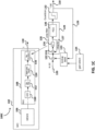
- FIG. 1D is a block diagram of a digital microphone 100D that implements dynamic parameter changes without causing significant audio artefacts, according to an embodiment. More specifically digital microphone 100D comprises a dynamic digital gain adjustment including a state detection and gain control block 138, and a variable gain block 136 in the feedback loop of the digital modulator 116. Digital microphone 100D also includes package 102, MEMS device 106, ASIC 108, ADC 110, digital filter 112, digital gain block 114, digital modulator 116, single-bit output 118, "m" bit input 120, summer 122, summer 124, block 126, block 128, loop filter 130, and quantizer 132, all previously described.
- a dynamic digital gain adjustment implementation located within digital modulator 116 includes a state detection and a variable gain control block 138 having an input coupled to the output of integrator stage 127 within digital modulator 116.
- State detection and gain control block 138 monitors the output of integrator stage 127 and determines whether or not the integrator stage 127 is at the mean value, or within threshold limits of the mean value. If integrator stage 127 is determined to be at the mean value, or within the threshold limits of the mean value, a control portion of state detection and gain control block 138 will generate an appropriate control signal (having a level such as a logic one, for example) indicating that the parameter change can be made.
- variable gain control block 136 is interposed into feedback loop 129 between the single-bit output 118 and an input of summer 122.
- variable gain control block 136 comprises an adjustable digital gain block having a control input for receiving the control signal from the state detection and gain control block 138.
- the control signal determines whether or not the gain of the control block can be changed, and, if so, the gain change level that is desired. In embodiments, very small gain adjustments can be frequently made without causing corresponding audio artefacts.
- Digital microphone 100D advantageously reduces or minimizes switching artefacts during a parameter switching event, and can be applied in a wide range of applications including digital and analog modulators, dynamic change of gains in modulators, dynamic change of sampling rates, and dynamic change of sampling capacitor values, which are described in further detail below.
- Digital microphone 100D advantageously provides dynamic parameter changes without additional group delay and with relatively low complexity circuit architecture. Additional filtering can be implemented, however, if the additional delay is acceptable for a given application.
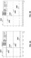
- Figure 2A is a graph 202A of input and output sequences of an integrator that will result in minimal audible transients due to the detection of a zero integrator state during a switching event, according to an embodiment.
- the integrator input sequence is shown as a series of "o" symbols 212A clustered at the maximum positive value 204A and at the maximum negative value 208A.
- the integrator output sequence is shown as a series of "+" symbols 210A clustered at the maximum positive value 204A, at the mean value 206A, and at the maximum negative value 208A.
- a parameter switching event 214A is designated by solid vertical line. It is important to note that in Figure 2A that the parameter switching event 214A occurs when the integrator output 210A is at the mean value 206A. Hence, the output of the digital microphone will only include minimal audible transients.
- Figure 2B is a graph 202B of input and output sequences of an integrator that will result in significant transients due to the detection of a non-zero integrator state during a switching event, according to an embodiment.
- the integrator input sequence is shown as a series of "o" symbols 212b clustered at the maximum positive value 204B and at the maximum negative value 208B.
- the integrator output sequence is shown as a series of "+" symbols 210B clustered at the maximum positive value 204B, at the mean value 206B, and at the maximum negative value 208B.
- a parameter switching event 214B is designated by solid vertical line. It is important to note that in Figure 2B that the parameter switching event 214A occurs when the integrator output 210A is at the maximum positive value 204B. Hence, the output of the digital microphone will include significant audible transients.
- Figure 3A is a graph 302A comparing a low-pass filter output for a digital microphone with and without dynamic seamless switching during a switching event (for a switched modulator input).
- Traces 304A, 306A, and 308A are the low-pass filter outputs for a digital microphone associated with a good selection of a switching time instant (when an output of the integrator of the digital microphone is at a mean value).
- Traces 304A, 306A, and 308A are relatively flat, indicating that there are no or minimal audible transients present during the switching event.
- Trace 310A is the low-pass filter output for a digital microphone associated with a bad selection of a switching time instant (when an output of the integrator of the digital microphone is at a maximum positive value or a maximum negative value). Trace 310A shows a pronounced peak, indicating that presence of a significant audible transient during the switching event.
- Figure 3B is a graph 302B comparing a low-pass filter output for a digital microphone with and without dynamic seamless switching during a switching event (for a zero modulator input).
- Traces 306B is the low-pass filter output for a digital microphone associated with a good selection of a switching time instant (when an output of the integrator of the digital microphone is at a mean value).
- Trace 306B is relatively flat, indicating that there are no or minimal audible transients present during the switching event.
- Trace 310B is the low-pass filter output for a digital microphone associated with a bad selection of a switching time instant (when an output of the integrator of the digital microphone is at a maximum positive value or a maximum negative value, for example).
- Trace 310B shows a pronounced peak during a switching event, indicating that presence of a significant audible transient during the switching event.
- Figure 4A is a block diagram of a state detector and control block 400A that can be used to monitor the output of an integrator in a digital microphone, according to an embodiment.
- State detect and control block 400A includes digital signal processing elements for monitoring the output state of the integrator and deciding whether or not the output state of the integrator is between a first threshold and a second threshold. If yes, state detector and control block 400A generates an appropriate output signal capable of switching a component within the digital microphone. For example, the output signal may be used to switch a variable gain block as previously described, or may be used to switch between differently valued switched capacitors, or may be used to switch between different clock frequencies in embodiments.
- the output of state detector and control block 400A may be one more control signals.
- state detector and control block 400A may include additional control circuitry such as switches and other control circuitry.
- Figure 4B is a block diagram 400B of a plurality of serially-coupled integrators 127A and 127B that can substitute for the single integrator of the digital microphone shown in Figure 1D , according to an embodiment.
- a first integrator 127A includes a first summer 124A and a first reciprocal Z transform transfer function block 126A.
- a second integrator 127B includes a second summer 124B and a second reciprocal Z transform transfer function block 126B.
- An input of second summer 124B is coupled to the output of the reciprocal Z transform transfer function block 126A. While only two integrator stages 127A and 127B are shown, any number can be used. For example, up to five serially-coupled integrators can be used in an embodiment.
- the output of the last integrator of the plurality of serially-coupled integrators is monitored by the state detection and control block 128 shown in Figure 1D .
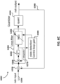
- FIG. 4C is a block diagram of an integrator 400C including a saturation block 402 that can be used for the single integrator of the digital microphone shown in Figure 1D , according to an embodiment.
- Integrator 400C includes a summer 124C and a reciprocal Z transform transfer function block 126C similar to those previously described, wherein an output of reciprocal Z transform transfer function block 126 is coupled to an input of summer 124C through unity gain feedback path 404.
- Saturation block 402 is interposed between summer 124C and reciprocal Z transform transfer function block to ensure that there is a more even distribution of integrator stage output states that may be required in some applications.
- FIG. 5A is a generalized block diagram of a digital microphone 500A having a dynamic parameter change in a digital modulator application, according to an embodiment.
- Digital microphone includes a package 102, a MEMS device 106, an ASIC 108, an ADC 110, a digital filter 112, a digital gain block 113, a digital modulator 116 and a single-bit output 118, all previous described.
- Digital microphone 500A includes a state detection and parameter control block 502A having an input coupled to the digital modulator 116 (at an output of one or more integrators) and an output for controlling one or more components (for example a variable gain block) with one or more control signals.
- the one more control signals can include a control signal 506A for controlling the frequency F s of a clock signal or other signal of the digital modulator 116, a control signal 508A for controlling the loop gain of the digital modulator 116 or the gain value of a gain block within the digital modulator 116, or a control signal 510A for controlling the value of other components, such as the capacitance of one or more switched capacitors in the digital modulator 116. While typically only one control signal is used, other embodiments can use more than one control signal to dynamically change more than one parameter simultaneously.
- FIG. 5B is a generalized block diagram of a digital microphone 500B having a dynamic parameter change in an ADC application, according to an embodiment.
- Digital microphone includes a package 102, a MEMS device 106, an ASIC 108, an ADC 110, a digital filter 112, a digital gain block 113, a digital modulator 116 and a single-bit output 118, all previous described.
- Digital microphone 500B includes a state detection and parameter control block 502B having an input coupled to the ADC 110 (at an output of one or more integrators) and an output for controlling one or more components (for example a variable gain block) with one or more control signals.
- the one more control signals can include a control signal 506B for controlling the frequency F s of a clock signal or other signal of the ADC 110, a control signal 508B for controlling the loop gain of the ADC 110 or the gain value of a gain block within the ADC 110, or a control signal 510B for controlling the value of other components, such as the capacitance of one or more switched capacitors in the ADC 110. While typically only one control signal is used, other embodiments can use more than one control signal to dynamically change more than one parameter simultaneously.
- Loop filter 630A can comprise a digital low pass filter, wherein the coefficients of the filter can be changed in different operational modes.
- the output of signal processing block 628A is coupled to the input of quantizer 632A, and the output of quantizer is coupled to the ADC output 634A, which is a single-bit output in an embodiment.
- a digital-to-analog converter 636A has an input coupled to ADC output 634A and an output coupled to an input of first summer 622A.
- Loop filter 630C can comprise a digital low pass filter.
- the output of signal processing block 628C is coupled to the input of quantizer 632C, and the output of quantizer is coupled to output 634A, which is a single-bit output in an embodiment.
- output 634A is a single-bit output in an embodiment.
- some or all of the components of digital modulator/ADC 600D can be fabricated in an ASIC 602C.
- the seamless dynamic parameter change is accomplished by the addition of the state detection and sampling rate control block 638C, which has an input coupled to the output of integrator 627C, an input for receiving a system clock 654C (clk), and an output 650C (sampling rate Fs) coupled to any of the components in ASIC 602C.
- the output 650C comprises a clock signal that has the same frequency as the system clock in a first mode of operation, and comprises a clock signal that has a lower frequency that the system clock in a second mode of operation.
- state detection and loop gain control block 638C can include a frequency divider or other digital signal processing components for generating the signal at output 650C.
- state detection and loop gain control block 638C can include an additional output 652C for distributing the signal at output 650C to any component within a digital microphone comprising the digital modulator/ADC 600D of Figure 6D .
- state detection and loop gain control block 638C can comprise first and second clock signal inputs and a switch for selecting between the first and second clock signal inputs to generate one or more of output 650C and output 652C.
- State detection and loop gain control block 638C monitors the output of integrator 627C and determines whether or not integrator 627C is in the mean integrator state or not. If so, state detection and loop gain control block 638C safely changes the frequency of the clock signal at output 650C and/or output 652C without generating audible artefacts. If not, the frequency of the clock signal at output 650C and/or output 652C remains constant and is not changed.
- FIG. 7 is a generalized block diagram 700 of a digital microphone 702 comprising a seamless dynamic parameter change capability.
- Digital microphone includes a MEMS device 704 coupled to an ASIC 712.
- ASIC 712 includes at least one integrator 706 coupled to a detection and control component 708, which is in turned coupled to one or more other components 710 of the digital microphone. At least one of the other components 710 provides an output signal at output 714.
- Digital components shown and described herein can be fabricated as digital circuit components in one or more integrated circuits.
- the digital components shown and described herein can also be implemented in a microprocessor executing instructions for providing the digital circuit component function.
- at least one of the digital components shown and described herein can be implemented as analog components.
- an analog modulator can be used.
- embodiment concepts can be implemented in an analog microphone having an integrator and a first (high performance) operational mode and a second (power saving) operational mode, wherein dynamic switching is desired between the first operational mode and the second operational mode, or within one of the operational modes, without generating significant audio artefacts during switching events.
Landscapes
- Engineering & Computer Science (AREA)
- Theoretical Computer Science (AREA)
- Physics & Mathematics (AREA)
- Acoustics & Sound (AREA)
- Signal Processing (AREA)
- Compression, Expansion, Code Conversion, And Decoders (AREA)
Claims (12)
- Ein digitales Mikrofon (100D, 500A, 500B, 702), das folgende Merkmale aufweist:zumindest einen Integrator (127, 127A, 127B, 400C, 627A, 627B, 627C, 706);eine Zustandserfassungs- und Parametersteuerkomponente (708), die direkt mit einem Ausgang des Integrators (127, 127A, 127B, 400C, 627A, 627B, 627C, 706) gekoppelt ist; undeine Signalverarbeitungskomponente, die mit einem Ausgang der Zustandserfassungs- und Parametersteuerkomponente (708) gekoppelt ist, wobei ein Parameter der Signalverarbeitungskomponente einen ersten Ausgangssignalwert in einem ersten Betriebsmodus und einen zweiten Ausgangssignalwert in einem zweiten Betriebsmodus aufweist, der sich von dem ersten Betriebsmodus unterscheidet, wobei der Parameter der Signalverarbeitungskomponente einen Verstärkungswert aufweist, wobei die Zustandserfassungs- und Parametersteuerkomponente (708) erste und zweite Schwellenwerte aufweist, wobei jeder der ersten und zweiten Schwellenwerte dem Integratorausgang entspricht, der sich von einem digitalen oder analogen Nullwert unterscheidet, und wobei die Signalverarbeitungskomponente eine variable Verstärkungskomponente aufweist, die konfiguriert ist zum Ändern des Verstärkungswerts, wenn der Ausgang des Integrators (127, 127A, 127B, 400C, 627A, 627B, 627C, 706) zwischen den ersten und zweiten Schwellenwerten liegt, so dass der Parameter der Signalverarbeitungskomponente in dem digitalen Mikrofon (100D, 500A, 500B, 702) sicher eingestellt werden kann, ohne hörbare Artefakte zu verursachen, wobei die Zustandserfassungs- und Parametersteuerkomponente (708) konfiguriert ist zum Erzeugen des ersten Ausgangssignalwerts, wenn der Ausgang des Integrators (127, 127A, 127B, 400C, 627A, 627B, 627C, 706) zwischen dem ersten Schwellenwert und dem zweiten Schwellenwert liegt, und zum Erzeugen des zweiten Ausgangssignalwerts, wenn der Ausgang des Integrators (127, 127A, 127B, 400C, 627A, 627B, 627C, 706) nicht zwischen dem ersten Schwellenwert und dem zweiten Schwellenwert liegt.
- Das digitale Mikrofon (100D, 500A, 500B, 702) gemäß Anspruch 1, wobei die Signalverarbeitungskomponente einen Analog-Digital-Wandler (ADC) oder einen digitalen Modulator (116, 600C, 600D) des digitalen Mikrofons (100D, 500A, 500B, 702) aufweist.
- Das digitale Mikrofon (100D, 500A, 500B, 702) gemäß einem der Ansprüche 1 bis 2, wobei der Parameter der Signalverarbeitungskomponente ferner eine Taktfrequenz des digitalen Mikrofons (100D, 500A, 500B, 702) oder eine Kapazität von einem oder mehreren geschalteten Kondensatoren in dem ADC (110) aufweist.
- Das digitale Mikrofon (100D, 500A, 500B, 702) gemäß einem der Ansprüche 1 bis 3, wobei der zumindest eine Integrator (127, 127A, 127B, 400C, 627A, 627B, 627C, 706) eine Mehrzahl von seriell gekoppelten Integratoren (127, 127A, 127B, 400C, 627A, 627B, 627C, 706) aufweist.
- Das digitale Mikrofon (100D, 500A, 500B, 702) gemäß einem der Ansprüche 1 bis 4, wobei der zumindest eine Integrator (127, 127A, 127B, 400C, 627A, 627B, 627C, 706), die Zustandserfassungs- und Parametersteuerkomponente (708) und die Signalverarbeitungskomponente in einer anwendungsspezifischen integrierten Schaltung, ASIC, (108, 602) hergestellt sind; und
wobei beispielsweise das digitale Mikrofon (100D, 500A, 500B, 702) ferner ein mikroelektromechanisches System, MEMS, (106) aufweisen kann, das mit der ASIC (108, 602) gekoppelt ist, wobei beispielsweise das MEMS (106) und die ASIC (108, 602) in einem Halbleitergehäuse (102) hergestellt sind. - Ein digitaler Modulator (116, 600C, 600D), der folgende Merkmale aufweist:einen Summierer (122, 124);zumindest einen Integrator (127, 127A, 127B, 400C, 627A, 627B, 627C, 706), der mit dem Summierer (122, 124) gekoppelt ist;einen Quantisierer (132, 632A, 632B, 632C), der mit dem zumindest einen Integrator (127, 127A, 127B, 400C, 627A, 627B, 627C, 706) gekoppelt ist;eine Zustandserfassungs- und Steuerkomponente (708), die mit einem Ausgang des zumindest einen Integrators (127, 127A, 127B, 400C, 627A, 627B, 627C, 706) gekoppelt ist; undeinen variablen Verstärkungsblock (136), der zwischen die Zustandserfassungs- und Steuerkomponente (708) und den Summierer (122, 124) gekoppelt ist, wobei die Zustandserfassungs- und Steuerkomponente (708) konfiguriert ist zum Erzeugen eines ersten Ausgangssignals, wenn ein Ausgang des Integrators (127, 127A, 127B, 400C, 627A, 627B, 627C, 706) zwischen einem ersten Schwellenwert und einem zweiten Schwellenwert liegt, und zum Erzeugen eines zweiten Ausgangssignals, wenn der Ausgang des Integrators (127, 127A, 127B, 400C, 627A, 627B, 627C, 706) nicht zwischen dem ersten Schwellenwert und dem zweiten Schwellenwert liegt;wobei der variable Verstärkungsblock (136) konfiguriert ist zum Aufweisen eines ersten Verstärkungswerts ansprechend auf das erste Ausgangssignal und zum Aufweisen eines zweiten Verstärkungswerts ansprechend auf das zweite Ausgangssignal.
- Der digitale Modulator (116, 600C, 600D) gemäß Anspruch 6, wobei der Summierer (122, 124) konfiguriert ist zum Empfangen eines "m"-Bit-Eingangssignals, wobei "m" eine ganze Zahl größer als eins ist, und wobei der Quantisierer (132, 632A, 632B, 632C) konfiguriert ist zum Vorsehen eines Einzelbit-Ausgangssignals.
- Der digitale Modulator (116, 600C, 600D) gemäß einem der Ansprüche 6 oder 7, wobei der zumindest eine Integrator (127, 127A, 127B, 400C, 627A, 627B, 627C, 706) eine Mehrzahl von seriell gekoppelten Integratoren (127, 127A, 127B, 400C, 627A, 627B, 627C, 706) aufweist.
- Der digitale Modulator (116, 600C, 600D) gemäß einem der Ansprüche 6 bis 8, der weiter einen Schleifenfilter (130, 630A, 630B, 630C) aufweist, der zwischen dem zumindest einen Integrator (127, 127A, 127B, 400C, 627A, 627B, 627C, 706) und dem Quantisierer (132, 632A, 632B, 632C) angeordnet ist.
- Ein Verfahren zum Betreiben eines digitalen Mikrofons (100D, 500A, 500B, 702), wobei das Verfahren folgende Schritte aufweist:Überwachen eines Zustands eines Integrators (127, 127A, 127B, 400C, 627A, 627B, 627C, 706) des digitalen Mikrofons (100D, 500A, 500B, 702);Erzeugen eines Ausgangssignals mit einem ersten Pegel während eines ersten Ausgangs des Integrators (127, 127A, 127B, 400C, 627A, 627B, 627C, 706) und einem zweiten Pegel während eines zweiten Ausgangs des Integrators (127, 127A, 127B, 400C, 627A, 627B, 627C, 706);Steuern eines Parameterwerts einer Signalverarbeitungskomponente des digitalen Mikrofons (100D, 500A, 500B, 702) mit dem Ausgangssignal, wobei der Parameter der Signalverarbeitungskomponente einen Schleifenverstärkungswert aufweist;Ändern eines Betriebsmodus des digitalen Mikrofons (100D, 500A, 500B, 702) nur während des ersten Zustands des Integrators (127, 127A, 127B, 400C, 627A, 627B, 627C, 706);Ändern der Schleifenverstärkung des digitalen Mikrofons (100D, 500A, 500B, 702), wenn der Zustand des Integrators (127, 127A, 127B, 400C, 627A, 627B, 627C, 706) innerhalb eines vorbestimmten Bereichs von Werten liegt, wobei die Schleifenverstärkungsänderung durch das Hinzufügen eines Zustandserfassungs- und Schleifenverstärkungssteuerblocks (638A) erreicht wird, der einen Eingang, der mit dem Ausgang des Integrators (627A) gekoppelt ist, und einen Ausgang, der mit einem Steuereingang des Schleifenfilters (630A) gekoppelt ist, aufweist; undErzeugen des ersten Pegels, wenn der erste Zustand des Integrators (127, 127A, 127B, 400C, 627A, 627B, 627C, 706) zwischen einem ersten Schwellenwert und einem zweiten Schwellenwert liegt, und zum Erzeugen des zweiten Pegels, wenn der zweite Zustand des Integrators (127, 127A, 127B, 400C, 627A, 627B, 627C, 706) nicht zwischen dem ersten Schwellenwert und dem zweiten Schwellenwert liegt, so dass der Parameter der Signalverarbeitungskomponente in dem digitalen Mikrofon (100D, 500A, 500B, 702) sicher eingestellt werden kann, ohne hörbare Artefakte zu verursachen.
- Das Verfahren gemäß Anspruch 10, wobei die Signalverarbeitungskomponente einen Analog-Digital-Wandler ADC) oder einen digitalen Modulator (116, 600C, 600D) des digitalen Mikrofons (100D, 500A, 500B, 702) aufweist.
- Das Verfahren gemäß Anspruch 10 oder 11, wobei der Parameterwert der Signalverarbeitungskomponente ferner einen Taktfrequenzwert des digitalen Mikrofons (100D, 500A, 500B, 702) oder einen Kapazitätswert von einem oder mehreren geschalteten Kondensatoren in dem ADC (110) aufweist.
Applications Claiming Priority (1)
| Application Number | Priority Date | Filing Date | Title |
|---|---|---|---|
| US17/395,077 US11659329B2 (en) | 2021-08-05 | 2021-08-05 | Efficient seamless switching of sigma-delta modulators |
Publications (3)
| Publication Number | Publication Date |
|---|---|
| EP4131995A1 EP4131995A1 (de) | 2023-02-08 |
| EP4131995B1 true EP4131995B1 (de) | 2025-03-26 |
| EP4131995B9 EP4131995B9 (de) | 2025-08-13 |
Family
ID=82786690
Family Applications (1)
| Application Number | Title | Priority Date | Filing Date |
|---|---|---|---|
| EP22188210.3A Active EP4131995B9 (de) | 2021-08-05 | 2022-08-02 | Effiziente nahtlose umschaltung von sigma-delta-modulatoren |
Country Status (4)
| Country | Link |
|---|---|
| US (2) | US11659329B2 (de) |
| EP (1) | EP4131995B9 (de) |
| KR (1) | KR20230021604A (de) |
| CN (1) | CN115914940A (de) |
Families Citing this family (2)
| Publication number | Priority date | Publication date | Assignee | Title |
|---|---|---|---|---|
| CN117870586B (zh) * | 2024-01-17 | 2024-07-26 | 天津大学 | 一种管道悬跨或沉降弯曲的检测装置及方法 |
| US20250247064A1 (en) * | 2024-01-25 | 2025-07-31 | Infineon Technologies Ag | Transients minimization of digital systems due to memory update |
Family Cites Families (16)
| Publication number | Priority date | Publication date | Assignee | Title |
|---|---|---|---|---|
| JPH10509544A (ja) | 1994-11-02 | 1998-09-14 | アドバンスト・マイクロ・ディバイシス・インコーポレーテッド | モノリシックpcオーディオ回路 |
| US6804291B1 (en) | 2000-02-22 | 2004-10-12 | Texas Instruments Incorporated | Device and method of digital gain programming using sigma-delta modulator |
| JP4530119B2 (ja) * | 2001-06-08 | 2010-08-25 | ルネサスエレクトロニクス株式会社 | ディジタルδςモジュレータおよびそれを用いたd/aコンバータ |
| US6473019B1 (en) * | 2001-06-21 | 2002-10-29 | Nokia Corporation | Low capacitance, low kickback noise input stage of a multi-level quantizer with dithering and multi-threshold generation for a multi-bit sigma-delta modulator |
| KR20080063267A (ko) | 2005-07-19 | 2008-07-03 | 아우디오아시스 에이/에스 | 프로그래밍 가능 마이크로폰 |
| CN101540608A (zh) | 2008-03-20 | 2009-09-23 | 扬智科技股份有限公司 | 降低静音时量化噪声的装置与方法 |
| GB2507332B (en) | 2012-10-26 | 2016-09-14 | Cirrus Logic Int Semiconductor Ltd | Digital/analogue conversion |
| US9106211B2 (en) * | 2013-03-13 | 2015-08-11 | Infineon Technologies Austria Ag | System and method for an oversampled data converter |
| US9799349B2 (en) * | 2015-04-24 | 2017-10-24 | Cirrus Logic, Inc. | Analog-to-digital converter (ADC) dynamic range enhancement for voice-activated systems |
| US9959856B2 (en) | 2015-06-15 | 2018-05-01 | Cirrus Logic, Inc. | Systems and methods for reducing artifacts and improving performance of a multi-path analog-to-digital converter |
| US9894437B2 (en) | 2016-02-09 | 2018-02-13 | Knowles Electronics, Llc | Microphone assembly with pulse density modulated signal |
| US10476455B1 (en) * | 2018-08-08 | 2019-11-12 | Cirrus Logic, Inc. | Apparatus and method of suppressing transient noise during transition for class-D amplifier system having one or more pulse width modulator output paths |
| US12325627B2 (en) | 2020-01-27 | 2025-06-10 | Infineon Technologies Ag | Configurable microphone using internal clock changing |
| US12302064B2 (en) | 2020-01-27 | 2025-05-13 | Infineon Technologies Ag | Configurable microphone using internal clock changing |
| US11139820B1 (en) | 2020-07-17 | 2021-10-05 | Infineon Technologies Ag | Efficient digital gain implementation in digital microphones |
| US11858808B2 (en) | 2021-03-23 | 2024-01-02 | Infineon Technologies Ag | System and method for fast mode change of a digital microphone using digital cross-talk compensation |
-
2021
- 2021-08-05 US US17/395,077 patent/US11659329B2/en active Active
-
2022
- 2022-08-02 EP EP22188210.3A patent/EP4131995B9/de active Active
- 2022-08-02 KR KR1020220096045A patent/KR20230021604A/ko active Pending
- 2022-08-04 CN CN202210933729.9A patent/CN115914940A/zh active Pending
-
2023
- 2023-04-11 US US18/298,854 patent/US12439204B2/en active Active
Also Published As
| Publication number | Publication date |
|---|---|
| US12439204B2 (en) | 2025-10-07 |
| CN115914940A (zh) | 2023-04-04 |
| KR20230021604A (ko) | 2023-02-14 |
| EP4131995A1 (de) | 2023-02-08 |
| US20230040501A1 (en) | 2023-02-09 |
| EP4131995B9 (de) | 2025-08-13 |
| US11659329B2 (en) | 2023-05-23 |
| US20230247359A1 (en) | 2023-08-03 |
Similar Documents
| Publication | Publication Date | Title |
|---|---|---|
| EP4131995B9 (de) | Effiziente nahtlose umschaltung von sigma-delta-modulatoren | |
| US11374589B2 (en) | Adaptive analog to digital converter (ADC) multipath digital microphones | |
| EP2653845B1 (de) | Sensorschaltung und Kalibrierverfahren | |
| US8913762B2 (en) | Capacitive transducer circuit and method | |
| US20250133354A1 (en) | Configurable microphone using internal clock changing | |
| US10499150B2 (en) | Microphone assembly with digital feedback loop | |
| US20250223155A1 (en) | Configurable microphone using internal clock changing | |
| CN113038341B (zh) | 电容式传感器组件及其操作方法、集成电路 | |
| JP2007522741A (ja) | デジタル・マイクロフォン | |
| KR20140096015A (ko) | 용량성 신호 소스에 의해 제공된 신호를 증폭하기 위한 시스템 및 집적 회로 | |
| CN101044685A (zh) | 信号接收机和移动通信设备 | |
| WO2006047155A1 (en) | An input common-mode voltage feedback circuit for continuous-time sigma-delta analog-to-digital converter | |
| JP3214981B2 (ja) | Agc機能付きデルタシグマ型a/d変換器 | |
| US20240322833A1 (en) | Efficient filtering architecture with reduced group delay for decompression using predictor | |
| US12401944B1 (en) | Microphone signal conversion module and microphone module | |
| EP3360256A1 (de) | Elektronische schaltung für ein mikrofon und mikrofon | |
| US11381911B1 (en) | Digital sensor assembly with selective dynamic element matching | |
| Thomsen et al. | TA 8.3 A 110dB THD, 18mW DAC Using Output Sampling and Feedback to Reduce Distortion |
Legal Events
| Date | Code | Title | Description |
|---|---|---|---|
| PUAI | Public reference made under article 153(3) epc to a published international application that has entered the european phase |
Free format text: ORIGINAL CODE: 0009012 |
|
| STAA | Information on the status of an ep patent application or granted ep patent |
Free format text: STATUS: THE APPLICATION HAS BEEN PUBLISHED |
|
| AK | Designated contracting states |
Kind code of ref document: A1 Designated state(s): AL AT BE BG CH CY CZ DE DK EE ES FI FR GB GR HR HU IE IS IT LI LT LU LV MC MK MT NL NO PL PT RO RS SE SI SK SM TR |
|
| STAA | Information on the status of an ep patent application or granted ep patent |
Free format text: STATUS: REQUEST FOR EXAMINATION WAS MADE |
|
| 17P | Request for examination filed |
Effective date: 20230517 |
|
| RBV | Designated contracting states (corrected) |
Designated state(s): AL AT BE BG CH CY CZ DE DK EE ES FI FR GB GR HR HU IE IS IT LI LT LU LV MC MK MT NL NO PL PT RO RS SE SI SK SM TR |
|
| GRAP | Despatch of communication of intention to grant a patent |
Free format text: ORIGINAL CODE: EPIDOSNIGR1 |
|
| STAA | Information on the status of an ep patent application or granted ep patent |
Free format text: STATUS: GRANT OF PATENT IS INTENDED |
|
| RIC1 | Information provided on ipc code assigned before grant |
Ipc: H03M 3/00 20060101ALN20241017BHEP Ipc: H04R 19/04 20060101ALN20241017BHEP Ipc: H04R 19/00 20060101ALN20241017BHEP Ipc: H04R 17/02 20060101ALN20241017BHEP Ipc: H03M 7/32 20060101ALI20241017BHEP Ipc: H04R 3/00 20060101ALI20241017BHEP Ipc: H04R 1/04 20060101AFI20241017BHEP |
|
| INTG | Intention to grant announced |
Effective date: 20241028 |
|
| RIC1 | Information provided on ipc code assigned before grant |
Ipc: H03M 3/00 20060101ALN20241018BHEP Ipc: H04R 19/04 20060101ALN20241018BHEP Ipc: H04R 19/00 20060101ALN20241018BHEP Ipc: H04R 17/02 20060101ALN20241018BHEP Ipc: H03M 7/32 20060101ALI20241018BHEP Ipc: H04R 3/00 20060101ALI20241018BHEP Ipc: H04R 1/04 20060101AFI20241018BHEP |
|
| P01 | Opt-out of the competence of the unified patent court (upc) registered |
Free format text: CASE NUMBER: APP_86/2025 Effective date: 20250102 |
|
| GRAS | Grant fee paid |
Free format text: ORIGINAL CODE: EPIDOSNIGR3 |
|
| GRAA | (expected) grant |
Free format text: ORIGINAL CODE: 0009210 |
|
| STAA | Information on the status of an ep patent application or granted ep patent |
Free format text: STATUS: THE PATENT HAS BEEN GRANTED |
|
| AK | Designated contracting states |
Kind code of ref document: B1 Designated state(s): AL AT BE BG CH CY CZ DE DK EE ES FI FR GB GR HR HU IE IS IT LI LT LU LV MC MK MT NL NO PL PT RO RS SE SI SK SM TR |
|
| REG | Reference to a national code |
Ref country code: GB Ref legal event code: FG4D |
|
| REG | Reference to a national code |
Ref country code: CH Ref legal event code: EP |
|
| REG | Reference to a national code |
Ref country code: DE Ref legal event code: R096 Ref document number: 602022012179 Country of ref document: DE |
|
| REG | Reference to a national code |
Ref country code: IE Ref legal event code: FG4D |
|
| PG25 | Lapsed in a contracting state [announced via postgrant information from national office to epo] |
Ref country code: RS Free format text: LAPSE BECAUSE OF FAILURE TO SUBMIT A TRANSLATION OF THE DESCRIPTION OR TO PAY THE FEE WITHIN THE PRESCRIBED TIME-LIMIT Effective date: 20250626 |
|
| PG25 | Lapsed in a contracting state [announced via postgrant information from national office to epo] |
Ref country code: FI Free format text: LAPSE BECAUSE OF FAILURE TO SUBMIT A TRANSLATION OF THE DESCRIPTION OR TO PAY THE FEE WITHIN THE PRESCRIBED TIME-LIMIT Effective date: 20250326 |
|
| REG | Reference to a national code |
Ref country code: LT Ref legal event code: MG9D |
|
| PG25 | Lapsed in a contracting state [announced via postgrant information from national office to epo] |
Ref country code: NO Free format text: LAPSE BECAUSE OF FAILURE TO SUBMIT A TRANSLATION OF THE DESCRIPTION OR TO PAY THE FEE WITHIN THE PRESCRIBED TIME-LIMIT Effective date: 20250626 |
|
| PG25 | Lapsed in a contracting state [announced via postgrant information from national office to epo] |
Ref country code: HR Free format text: LAPSE BECAUSE OF FAILURE TO SUBMIT A TRANSLATION OF THE DESCRIPTION OR TO PAY THE FEE WITHIN THE PRESCRIBED TIME-LIMIT Effective date: 20250326 |
|
| PG25 | Lapsed in a contracting state [announced via postgrant information from national office to epo] |
Ref country code: LV Free format text: LAPSE BECAUSE OF FAILURE TO SUBMIT A TRANSLATION OF THE DESCRIPTION OR TO PAY THE FEE WITHIN THE PRESCRIBED TIME-LIMIT Effective date: 20250326 |
|
| PG25 | Lapsed in a contracting state [announced via postgrant information from national office to epo] |
Ref country code: BG Free format text: LAPSE BECAUSE OF FAILURE TO SUBMIT A TRANSLATION OF THE DESCRIPTION OR TO PAY THE FEE WITHIN THE PRESCRIBED TIME-LIMIT Effective date: 20250326 Ref country code: GR Free format text: LAPSE BECAUSE OF FAILURE TO SUBMIT A TRANSLATION OF THE DESCRIPTION OR TO PAY THE FEE WITHIN THE PRESCRIBED TIME-LIMIT Effective date: 20250627 |
|
| REG | Reference to a national code |
Ref country code: NL Ref legal event code: MP Effective date: 20250326 |
|
| REG | Reference to a national code |
Ref country code: CH Ref legal event code: PK Free format text: BERICHTIGUNG B9 |
|
| PG25 | Lapsed in a contracting state [announced via postgrant information from national office to epo] |
Ref country code: NL Free format text: LAPSE BECAUSE OF FAILURE TO SUBMIT A TRANSLATION OF THE DESCRIPTION OR TO PAY THE FEE WITHIN THE PRESCRIBED TIME-LIMIT Effective date: 20250326 |
|
| PG25 | Lapsed in a contracting state [announced via postgrant information from national office to epo] |
Ref country code: SE Free format text: LAPSE BECAUSE OF FAILURE TO SUBMIT A TRANSLATION OF THE DESCRIPTION OR TO PAY THE FEE WITHIN THE PRESCRIBED TIME-LIMIT Effective date: 20250326 |
|
| REG | Reference to a national code |
Ref country code: AT Ref legal event code: MK05 Ref document number: 1780184 Country of ref document: AT Kind code of ref document: T Effective date: 20250326 |
|
| PG25 | Lapsed in a contracting state [announced via postgrant information from national office to epo] |
Ref country code: SM Free format text: LAPSE BECAUSE OF FAILURE TO SUBMIT A TRANSLATION OF THE DESCRIPTION OR TO PAY THE FEE WITHIN THE PRESCRIBED TIME-LIMIT Effective date: 20250326 |
|
| PG25 | Lapsed in a contracting state [announced via postgrant information from national office to epo] |
Ref country code: ES Free format text: LAPSE BECAUSE OF FAILURE TO SUBMIT A TRANSLATION OF THE DESCRIPTION OR TO PAY THE FEE WITHIN THE PRESCRIBED TIME-LIMIT Effective date: 20250326 Ref country code: PT Free format text: LAPSE BECAUSE OF FAILURE TO SUBMIT A TRANSLATION OF THE DESCRIPTION OR TO PAY THE FEE WITHIN THE PRESCRIBED TIME-LIMIT Effective date: 20250728 |
|
| PG25 | Lapsed in a contracting state [announced via postgrant information from national office to epo] |
Ref country code: IT Free format text: LAPSE BECAUSE OF FAILURE TO SUBMIT A TRANSLATION OF THE DESCRIPTION OR TO PAY THE FEE WITHIN THE PRESCRIBED TIME-LIMIT Effective date: 20250326 Ref country code: PL Free format text: LAPSE BECAUSE OF FAILURE TO SUBMIT A TRANSLATION OF THE DESCRIPTION OR TO PAY THE FEE WITHIN THE PRESCRIBED TIME-LIMIT Effective date: 20250326 |
|
| PG25 | Lapsed in a contracting state [announced via postgrant information from national office to epo] |
Ref country code: AT Free format text: LAPSE BECAUSE OF FAILURE TO SUBMIT A TRANSLATION OF THE DESCRIPTION OR TO PAY THE FEE WITHIN THE PRESCRIBED TIME-LIMIT Effective date: 20250326 |
|
| PG25 | Lapsed in a contracting state [announced via postgrant information from national office to epo] |
Ref country code: RO Free format text: LAPSE BECAUSE OF FAILURE TO SUBMIT A TRANSLATION OF THE DESCRIPTION OR TO PAY THE FEE WITHIN THE PRESCRIBED TIME-LIMIT Effective date: 20250326 |
|
| PG25 | Lapsed in a contracting state [announced via postgrant information from national office to epo] |
Ref country code: SK Free format text: LAPSE BECAUSE OF FAILURE TO SUBMIT A TRANSLATION OF THE DESCRIPTION OR TO PAY THE FEE WITHIN THE PRESCRIBED TIME-LIMIT Effective date: 20250326 |
|
| PG25 | Lapsed in a contracting state [announced via postgrant information from national office to epo] |
Ref country code: IS Free format text: LAPSE BECAUSE OF FAILURE TO SUBMIT A TRANSLATION OF THE DESCRIPTION OR TO PAY THE FEE WITHIN THE PRESCRIBED TIME-LIMIT Effective date: 20250726 |
|
| REG | Reference to a national code |
Ref country code: DE Ref legal event code: R097 Ref document number: 602022012179 Country of ref document: DE |
|
| PGFP | Annual fee paid to national office [announced via postgrant information from national office to epo] |
Ref country code: DE Payment date: 20251021 Year of fee payment: 4 |
|
| PG25 | Lapsed in a contracting state [announced via postgrant information from national office to epo] |
Ref country code: DK Free format text: LAPSE BECAUSE OF FAILURE TO SUBMIT A TRANSLATION OF THE DESCRIPTION OR TO PAY THE FEE WITHIN THE PRESCRIBED TIME-LIMIT Effective date: 20250326 |
|
| PG25 | Lapsed in a contracting state [announced via postgrant information from national office to epo] |
Ref country code: CZ Free format text: LAPSE BECAUSE OF FAILURE TO SUBMIT A TRANSLATION OF THE DESCRIPTION OR TO PAY THE FEE WITHIN THE PRESCRIBED TIME-LIMIT Effective date: 20250326 |
|
| PLBE | No opposition filed within time limit |
Free format text: ORIGINAL CODE: 0009261 |
|
| STAA | Information on the status of an ep patent application or granted ep patent |
Free format text: STATUS: NO OPPOSITION FILED WITHIN TIME LIMIT |
|
| REG | Reference to a national code |
Ref country code: CH Ref legal event code: L10 Free format text: ST27 STATUS EVENT CODE: U-0-0-L10-L00 (AS PROVIDED BY THE NATIONAL OFFICE) Effective date: 20260211 |
|
| 26N | No opposition filed |
Effective date: 20260105 |
|
| REG | Reference to a national code |
Ref country code: CH Ref legal event code: H13 Free format text: ST27 STATUS EVENT CODE: U-0-0-H10-H13 (AS PROVIDED BY THE NATIONAL OFFICE) Effective date: 20260324 |
|
| PG25 | Lapsed in a contracting state [announced via postgrant information from national office to epo] |
Ref country code: MC Free format text: LAPSE BECAUSE OF FAILURE TO SUBMIT A TRANSLATION OF THE DESCRIPTION OR TO PAY THE FEE WITHIN THE PRESCRIBED TIME-LIMIT Effective date: 20250326 |
|
| PG25 | Lapsed in a contracting state [announced via postgrant information from national office to epo] |
Ref country code: LU Free format text: LAPSE BECAUSE OF NON-PAYMENT OF DUE FEES Effective date: 20250802 |
|
| PG25 | Lapsed in a contracting state [announced via postgrant information from national office to epo] |
Ref country code: CH Free format text: LAPSE BECAUSE OF NON-PAYMENT OF DUE FEES Effective date: 20250831 |