EP4131655A1 - Wireless transmission system - Google Patents
Wireless transmission system Download PDFInfo
- Publication number
- EP4131655A1 EP4131655A1 EP20929502.1A EP20929502A EP4131655A1 EP 4131655 A1 EP4131655 A1 EP 4131655A1 EP 20929502 A EP20929502 A EP 20929502A EP 4131655 A1 EP4131655 A1 EP 4131655A1
- Authority
- EP
- European Patent Office
- Prior art keywords
- electromagnetic wave
- reflector
- production line
- base station
- reflection
- Prior art date
- Legal status (The legal status is an assumption and is not a legal conclusion. Google has not performed a legal analysis and makes no representation as to the accuracy of the status listed.)
- Granted
Links
Images







Classifications
-
- H—ELECTRICITY
- H04—ELECTRIC COMMUNICATION TECHNIQUE
- H04B—TRANSMISSION
- H04B7/00—Radio transmission systems, i.e. using radiation field
- H04B7/14—Relay systems
- H04B7/145—Passive relay systems
-
- H—ELECTRICITY
- H01—ELECTRIC ELEMENTS
- H01Q—ANTENNAS, i.e. RADIO AERIALS
- H01Q1/00—Details of, or arrangements associated with, antennas
- H01Q1/12—Supports; Mounting means
- H01Q1/22—Supports; Mounting means by structural association with other equipment or articles
- H01Q1/24—Supports; Mounting means by structural association with other equipment or articles with receiving set
- H01Q1/241—Supports; Mounting means by structural association with other equipment or articles with receiving set used in mobile communications, e.g. GSM
- H01Q1/246—Supports; Mounting means by structural association with other equipment or articles with receiving set used in mobile communications, e.g. GSM specially adapted for base stations
-
- H—ELECTRICITY
- H01—ELECTRIC ELEMENTS
- H01Q—ANTENNAS, i.e. RADIO AERIALS
- H01Q15/00—Devices for reflection, refraction, diffraction or polarisation of waves radiated from an antenna, e.g. quasi-optical devices
- H01Q15/0006—Devices acting selectively as reflecting surface, as diffracting or as refracting device, e.g. frequency filtering or angular spatial filtering devices
- H01Q15/0086—Devices acting selectively as reflecting surface, as diffracting or as refracting device, e.g. frequency filtering or angular spatial filtering devices said selective devices having materials with a synthesized negative refractive index, e.g. metamaterials or left-handed materials
-
- H—ELECTRICITY
- H01—ELECTRIC ELEMENTS
- H01Q—ANTENNAS, i.e. RADIO AERIALS
- H01Q15/00—Devices for reflection, refraction, diffraction or polarisation of waves radiated from an antenna, e.g. quasi-optical devices
- H01Q15/14—Reflecting surfaces; Equivalent structures
-
- H—ELECTRICITY
- H01—ELECTRIC ELEMENTS
- H01Q—ANTENNAS, i.e. RADIO AERIALS
- H01Q19/00—Combinations of primary active antenna elements and units with secondary devices, e.g. with quasi-optical devices, for giving the antenna a desired directional characteristic
- H01Q19/10—Combinations of primary active antenna elements and units with secondary devices, e.g. with quasi-optical devices, for giving the antenna a desired directional characteristic using reflecting surfaces
- H01Q19/104—Combinations of primary active antenna elements and units with secondary devices, e.g. with quasi-optical devices, for giving the antenna a desired directional characteristic using reflecting surfaces using a substantially flat reflector for deflecting the radiated beam, e.g. periscopic antennas
-
- H—ELECTRICITY
- H01—ELECTRIC ELEMENTS
- H01Q—ANTENNAS, i.e. RADIO AERIALS
- H01Q19/00—Combinations of primary active antenna elements and units with secondary devices, e.g. with quasi-optical devices, for giving the antenna a desired directional characteristic
- H01Q19/10—Combinations of primary active antenna elements and units with secondary devices, e.g. with quasi-optical devices, for giving the antenna a desired directional characteristic using reflecting surfaces
- H01Q19/18—Combinations of primary active antenna elements and units with secondary devices, e.g. with quasi-optical devices, for giving the antenna a desired directional characteristic using reflecting surfaces having two or more spaced reflecting surfaces
-
- H—ELECTRICITY
- H01—ELECTRIC ELEMENTS
- H01Q—ANTENNAS, i.e. RADIO AERIALS
- H01Q3/00—Arrangements for changing or varying the orientation or the shape of the directional pattern of the waves radiated from an antenna or antenna system
- H01Q3/44—Arrangements for changing or varying the orientation or the shape of the directional pattern of the waves radiated from an antenna or antenna system varying the electric or magnetic characteristics of reflecting, refracting, or diffracting devices associated with the radiating element
- H01Q3/46—Active lenses or reflecting arrays
-
- H—ELECTRICITY
- H04—ELECTRIC COMMUNICATION TECHNIQUE
- H04B—TRANSMISSION
- H04B7/00—Radio transmission systems, i.e. using radiation field
- H04B7/02—Diversity systems; Multi-antenna system, i.e. transmission or reception using multiple antennas
- H04B7/04—Diversity systems; Multi-antenna system, i.e. transmission or reception using multiple antennas using two or more spaced independent antennas
- H04B7/04013—Intelligent reflective surfaces
-
- H—ELECTRICITY
- H01—ELECTRIC ELEMENTS
- H01Q—ANTENNAS, i.e. RADIO AERIALS
- H01Q1/00—Details of, or arrangements associated with, antennas
- H01Q1/36—Structural form of radiating elements, e.g. cone, spiral, umbrella; Particular materials used therewith
- H01Q1/364—Structural form of radiating elements, e.g. cone, spiral, umbrella; Particular materials used therewith using a particular conducting material, e.g. superconductor
Definitions
- the radio communication environments in production facilities such as factories or plants are different from the environment of the public cellular communication networks.
- electromagnetic wave reflector With the electromagnetic wave reflector, radio propagation in mobile communications, including the wireless transmission system, at production facilities such as factories or plants can be improved.
- Base stations BS1 and BS2 are provided to connect the machines and equipment in the production line to the network.
- Machines M1 and M2 used in the production line are equipped with wireless transceiver units WT1 and WT2, respectively, to access at least one of the base stations BS1 and BS2 for the connection to the network.
- Equipment used in the production line 3 includes all kinds of equipment involved in the production, such as microdevices including sensors and actuators, assembling equipment, manufacturing machines, or management systems.
- the equipment in the production line 3 is not limited to static devices or machines, but includes mobile devices and machines capable of moving freely in the production line 3.
- the reflective surface 105 of the electromagnetic wave reflector 10 is configured to reflect the radio waves in the frequency band from 1 GHz to 170 GHz.
- the reflective surface 105 may include a normal reflector 101, which provides regular reflection with an angle of reflection the same as the angle of incidence, and/or a meta-reflector 102, which has an artificial surface capable of controlling the reflection characteristics of the incident electromagnetic waves.
- a "meta-reflector” is a kind of "metasurface” representing an artificial surface that regulates the transmission and/or reflection characteristics of the incident electromagnetic waves.
- a large number of scatterers sufficiently smaller than the wavelength are arranged in the meta-reflector to regulate the reflection phase distribution and the amplitude distribution, thereby reflecting the incident radio waves in a direction other than that of specular reflection.
- the meta-reflector 102 may be designed so as to provide diffusion and wave-front formation at a predetermined angular distribution, in addition to the meta-reflection in directions other than the specular reflection.
- FIG. 8 shows an example of the electrical connector part 15 of the support body 11 in a cross-sectional view taken along a horizontal plane when the electromagnetic wave reflector 10 stands up on the plane P (see FIG. 7 ).
- the electrical connector part 15 is designed to propagate the reference potential of reflection from one panel to the adjacent panel so that the reference potential of the reflection phenomenon is shared between the adjacent panels 13.
- the CFRP which holds the edge jackets 17-1 and 17-2, serves by itself as the electrical connector part 15A. Electrical connection can be established between the edge jackets 17-1 and 17-2 without using a bridge electrode 112.
- carbon fiber has better reflective performance than bulk metal, and the reflective characteristics of the frame 111A can be improved.
- FIG. 10D shows a configuration of an electrical connector part 15D of a support body 11D.
- the electrical connector part 15D has a bridge electrode 114 that electrically connects the edge jackets 17-1 and 17-2.
- the bridge electrode 114 connects the bottom surfaces 172 of the edge jackets 17-1 and 17-2.
- the configuration of FIG. 10D is advantageous in that the high frequency current can flow in the shortest path from the conductor 131-1 to the along the shortest path through the edge jacket 17-1, the bridge electrode 114, the edge jacket 17-2, and the conductor 131-2.
- FIG. 10E shows a configuration using a frame 111E of a composite type of metal and resin.
- the frame 111E has a metal connector 141 and a resin reinforcement 142 that covers the metal connector 141.
- the metal connector 141 can be easily manufactured by extrusion molding or the like, and the connector itself has a certain degree of strength while ensuring electrical connection.
- the resin reinforcement 142 may be formed of an adhesive such as an acrylic adhesive or an epoxy adhesive, thereby reducing the thickness of the metal connector 141 and suppressing residual inductance caused by current detours.
- the corners may be rounded to prevent diffraction at the corners.
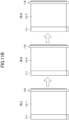
- FIG. 11B shows the state of the electromagnetic wave reflectors 10 before connection.
- a frame 111 having an electrical connector part 15 is attached in advance to one of the side edges of the panel 13, and a guide beam 118 is attached to the other side edge.
- the reflective surfaces 105 of the electromagnetic wave reflector 10-1 to 10-3 may have any configuration shown in FIG. 6A to FIG. 6D .
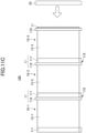
- a base 119 may be provided in advance to one or both of the guide beam 118 and the frame 111, thereby allowing the connected electromagnetic wave reflectors 10-1 to 10-3 to stand up by themselves on the installation plane.
- a cover 29 may be provided to the edge of the last panel 13 of the electromagnetic wave reflector 10-3 at the end position to protect the edge jacket 17 and the guide beam 118.
- FIG. 12 and FIG. 13 show a mechanism that reinforces the connections of a plurality of electromagnetic wave reflectors 10-1 and 10-2.
- FIG. 12 (A) is a front view of the electromagnetic wave reflective fence 100, (B) is a side view before the reinforcing mechanism 125 is tightened, and (C) is a side view after the reinforcing mechanism 125 is tightened.
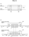
- FIG. 13 shows a configuration example of the reinforcement mechanism 125.
- FIG. 13 shows a front view of guide grooves 129 formed in an attaching surface 127a of a cover 127 of the reinforcement mechanism 125, and cross-sectional views taken along the cross-sections A and B of the front view. The cover 127 is attached to the panels 13 at the attaching surface 127a.
- the mechanism for reinforcing the connection between multiple electromagnetic wave reflectors 10 is not limited to the above-described example shown in FIG. 12 and FIG. 13 , and other appropriate mechanisms including a fastener and a ratchet may be used unless the electromagnetic wave reflection characteristics are impaired.
- the design of the edge jacket 17 and the electrical connector part 15 may be appropriately modified assuming the above-described pressure contact process.
- FIG. 14 shows the size of the meta-reflector 102, assuming that a transmitter "Tx" and a receiver “Rx" are used.
- the transmitter Tx is, for example, a base station BS.
- Receiver Rx is, for example, equipment located in the production line 3.
- the distance from the transmitter Tx to the surface 102s of the meta-reflector 102 is denoted as d1, and the distance from the surface 102s of the meta-reflector 102 to the receiver Rx is denoted as d2.
- the standard length of the production line is 80 m.
- the radius R of the first Fresnel zone is 0.770 m.
- the radius R is 0.588 m.
- the similar estimation applies to the normal reflector 101 because the radius R of the first Fresnel zone does not depend on the relationship between the angle of incidence and the angle of reflection.
- the size of the normal reflector 101 is desirably 50 centimeters per side.
- the meta-reflector 102 is used in a production line covered by a service area with a large aspect ratio, the oblique angle of either incidence or reflection becomes deep. So, the layout and the positional relationship among the production line 3, the base station BS, and the electromagnetic wave reflector 10 will be discussed below.
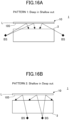
- FIG. 16B shows Pattern 2 of reflection.
- the base stations BS and the production line 3 are laid in such a positional relationship that the radio waves emitted from the base stations BS are incident onto the reflective surface 105 at a shallow angle with respect to the normal to the reflective surface 105 and are reflected at an angle deeper than the incident angle.
- the radio waves are incident onto the reflective surface 105 at an angle of incidence of 45 degrees or less, and are reflected at an angle greater than the regular reflection.
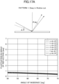
- FIG. 17A shows the baseline robustness of Pattern 1
- FIG. 31B shows the baseline robustness of Pattern 2.
- the baseline robustness means the stability of the angle of reflection when the angle of incidence is changed by 1 degree.
- the baseline robustness is high if the change in the reflection angle is small with respect to the change in the incident angle of 1 degree.
- the base stations BS are preferably located so that the incident angle of the radio waves emitted from the base stations BS and incident onto the electromagnetic wave reflector 10 is 50° or greater, from the viewpoint of suppressing the fluctuation of the reflection angle depending on the incident angle. Therefore, the layout shown in FIG. 17A is preferable to the layout of FIG. 16B .
- FIG. 18 shows quantification of the baseline robustness.
- the baseline robustness of FIG. 17A and FIG. 17B can be estimated by the following procedure.
- a phase jump ⁇ (x) is determined by inputting a certain incident angle ⁇ i and a reflection angle ⁇ r to a function f for calculating a phase jump distribution, where x denotes the position in the x-direction on the reflective surface.
- a phase jump represents the amount of phase to be added to a reflected wave to guide the reflected wave to a desired direction.
- FIG. 17A and FIG. 17B are plots of the calculated fluctuation of the reflection angle as a function of the angle of incidence.
- the equipment in the production line 3 does not always receive only the radio waves reflected from the electromagnetic wave reflector 10, but can receive the radio waves directly from the base station BS. In this case, receive diversity can be achieved by in-phase signal reception. If two base stations BS are provided at both ends of the elongated production line 3, cooperative type base stations may be used.
Landscapes
- Engineering & Computer Science (AREA)
- Computer Networks & Wireless Communication (AREA)
- Physics & Mathematics (AREA)
- Electromagnetism (AREA)
- Signal Processing (AREA)
- Aerials With Secondary Devices (AREA)
Abstract
Description
- The present invention relates to an electromagnetic wave reflector, an electromagnetic wave reflective fence, and a method of assembling an electromagnetic wave reflector.
- The industrial internet of things (IoT), which is adapted to automate manufacturing processes and introduce advanced production/process control and predictive maintenance into production sites, is progressing. Among industrial IoT, "smart factory" connects devices, equipment, and management systems in the factory to the cloud and/or edge artificial intelligence (AI) to streamline the manufacturing process. It is expected that a high-speed, low-latency, and large-capacity mobile communication technology of multi-connectivity, such as the fifth generation networks (5G), is to be introduced into industrial IoT communication networks to deal with a huge amount of data. In addition to the inherent mobility and flexibility of the mobile communication technology, low latency of the 5G networks is considered to be suitable for industrial IoT.
- A joint structure for translucent electromagnetic shielding plates has been proposed, which is used in facilities such as intelligent buildings. See, for example,
Patent Document 1 presented below. - Patent Document 1:
JP 4892207 B - The radio communication environments in production facilities such as factories or plants are different from the environment of the public cellular communication networks. There are various machines and structures in production facilities, which cause interference with radio propagation and make it difficult to achieve high quality wireless communication.
- One of the objectives of the present invention is to provide a technique of improving radio propagation in mobile communications in production facilities.
- In one aspect of the disclosure, a wireless transmission system includes a base station that transmits and receives a radio wave in a frequency band selected from a range of 1 GHz to 170 GHz, and an electromagnetic wave reflector having a reflective surface that reflects the radio wave and provided along at least a part of a production line in which manufacturing equipment that transmits and receives the radio wave is used.
- With the electromagnetic wave reflector, radio propagation in mobile communications, including the wireless transmission system, at production facilities such as factories or plants can be improved.
-
-
FIG. 1 is a schematic diagram of a production line in a factory, to which the present disclosure is applied; -
FIG. 2 is a schematic plan view of a wireless transmission system using an electromagnetic wave reflector according to an embodiment; -
FIG. 3A is a diagram showing regular reflection with the angle of reflection equal to the angle of incidence; -
FIG. 3B is a diagram showing reflection at an angle of reflection different from the angle of incidence; -
FIG. 3C is a diagram showing diffusion in a plurality of directions; -
FIG. 4 is a diagram showing the basic concept of the electromagnetic wave reflector according to an embodiment; -
FIG. 5A shows a modification of the electromagnetic wave reflector; -
FIG. 5B shows another modification of the electromagnetic wave reflector; -
FIG. 5C shows yet another modification of the electromagnetic wave reflector; -
FIG. 5D shows still another modification of the electromagnetic wave reflector; -
FIG. 6A shows a configuration example of a reflective surface; -
FIG. 6B shows another configuration example of the reflective surface; -
FIG. 6C shows yet another configuration example of the reflective surface; -
FIG. 6D shows still another configuration example of the reflective surface; -
FIG. 7 shows a configuration example in which electromagnetic wave reflectors are connected; -
FIG. 8 is a schematic diagram of a connector part of a support body; -
FIG. 9A shows an example of edge finishing of a panel; -
FIG. 9B shows another example of edge finishing of the panel; -
FIG. 10A shows a configuration example of the connector part; -
FIG. 10B shows another configuration example of the connector part; -
FIG. 10C shows yet another configuration example of the connector part; -
FIG. 10D shows still another configuration example of the connector part; -
FIG. 10E shows still another configuration example of the connector part; -
FIG. 10F shows a typical configuration of the connector part, as a reference configuration; -
FIG.11A illustrates how multiple panels are connected; -
FIG. 11B shows the state of the electromagnetic wave reflectors before connection; -
FIG. 11C shows the state of the electromagnetic wave reflectors after connection; -
FIG. 12 shows an example of reinforcement of the connected electromagnetic wave reflectors; -
FIG. 13 shows an example of a fastening mechanism; -
FIG. 14 illustrates how the size of a meta-reflector is determined; -
FIG. 15 shows zone sizes depending on the operating frequency and the positional relationship between a transmitter and a receiver; -
FIG. 16A shows a positional relationship of a wireless transmission system; -
FIG. 16B shows another positional relationship of a wireless transmission system; -
FIG. 17A shows reference robustness ofreflection pattern 1; -
FIG. 17B shows reference robustness ofreflection pattern 2; -
FIG. 18 shows quantification of the baseline robustness; -
FIG. 19A shows changes in the phase jump ofreflection pattern 1; and -
FIG. 19B shows changes in phase jumps ofreflection pattern 2. -
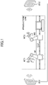
FIG. 1 is a schematic diagram of a production line in a factory to which the present disclosure may be applied. A production line is a belt-like production site in which facilities and equipment for assembling or manufacturing are provided as a sequence of flow. Industrial IoT improves production efficiency and ensures on-site safety by connecting industrial machines, equipment, and management systems used in production lines to networks. - Base stations BS1 and BS2 are provided to connect the machines and equipment in the production line to the network. Machines M1 and M2 used in the production line are equipped with wireless transceiver units WT1 and WT2, respectively, to access at least one of the base stations BS1 and BS2 for the connection to the network.
- In order to establish wireless connection between the equipment in the production line and the network, the base stations BS1 and BS2 (hereinafter referred to collectively as "BS" as necessary) are adapted to form a horizontally elongated rectangular service area. According to the technical specifications (TS22.104) of the 3rd Generation Partnership Project (3GPP), a mobile communications standardization organization, the aspect ratio of 3 to 5 of the rectangular area in a horizontal plane is stipulated as a system requirement. For example, dimensions (length)x(width)x(height) of a use case named "Motion Control" are defined as 50
m x 10 m x 10 m. - It may be effective to locate the base stations BS1 and BS2 at both ends of the elongated production line in terms of the coverage, so as to cover the production line and establish network connections for the machines M1 and M1 within the service areas provided by the base stations BS1 and BS2. The base stations BS1 and BS2 may cooperate with each other to improve the coverage and the quality of radio communication. The details of the positional relationship of the base stations BS with respect to the production line will be described later.
-
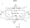
FIG. 2 is a schematic plan view of awireless transmission system 1 using anelectromagnetic wave reflector 10 according to an embodiment. Thewireless transmission system 1 includes aproduction line 3, in which production equipment capable of transmitting and receiving radio waves is provided, a base station BS that wirelessly communicates with the equipment in theproduction line 3, and one or moreelectromagnetic wave reflectors 10 provided along theproduction line 3. Theelectromagnetic wave reflector 10 has areflective surface 105 that reflects radio waves. The plane in which the production line is provided is the XY plane, and the height direction perpendicular to the XY plane is the Z direction. - Equipment used in the
production line 3 includes all kinds of equipment involved in the production, such as microdevices including sensors and actuators, assembling equipment, manufacturing machines, or management systems. The equipment in theproduction line 3 is not limited to static devices or machines, but includes mobile devices and machines capable of moving freely in theproduction line 3. - The base stations BS1 and BS2 transmit and receive radio waves to and from the machines M1 and M2 (see
FIG. 1 ) having wireless communication functions, at a specific frequency band selected from the range of 1 GHz to 170 GHz. The in-line objects and the peripheral structures (such as ducts or pipes) of the production line are often made of metal, and the radio waves are reflected or shielded by the metal objects or structures. Besides, straightness of a highfrequency radio wave such as millimeter wave causes little diffraction, which makes it difficult for the radio wave to reach far. For the equipment located at or near the center of theproduction line 3, the communication environment tends to be deteriorated due to interference with the radio waves reflected from the nearby equipment or metal products being manufactured in theproduction line 3. - The wireless communication quality could be maintained by providing a large number of base stations along the longitudinal axis of the
production line 3; however, efficient use of the work space is disturbed and installation cost will increase. Thewireless transmission system 1 solves these problems by providing anelectromagnetic wave reflector 10 along the longitudinal axis of theproduction line 3, and by providing a base station BS at an end of theproduction line 3 in the longitudinal direction. Owing to theelectromagnetic wave reflector 10, the number of base stations installed in the production facility can be reduced, and the wireless communication environment between the base station BS and equipment and devices in theproduction line 3 can be improved. - The
electromagnetic wave reflector 10 may be installed along at least a part of theproduction line 3 so as to be substantially parallel to the long axis of theproduction line 3. In the context of the term "substantially parallel", it is unnecessary for theelectromagnetic wave reflector 10 to be arranged strictly parallel to the long axis of theproduction line 3. Theelectromagnetic wave reflector 10 may be slightly tilted with respect to the long axis of theproduction line 3 within an acceptable range as long as the radio waves are efficiently transmitted and received between the base station BS and the equipment or devices in theproduction line 3. - The
reflective surface 105 of theelectromagnetic wave reflector 10 is configured to reflect the radio waves in the frequency band from 1 GHz to 170 GHz. Thereflective surface 105 may include anormal reflector 101, which provides regular reflection with an angle of reflection the same as the angle of incidence, and/or a meta-reflector 102, which has an artificial surface capable of controlling the reflection characteristics of the incident electromagnetic waves. A "meta-reflector" is a kind of "metasurface" representing an artificial surface that regulates the transmission and/or reflection characteristics of the incident electromagnetic waves. A large number of scatterers sufficiently smaller than the wavelength are arranged in the meta-reflector to regulate the reflection phase distribution and the amplitude distribution, thereby reflecting the incident radio waves in a direction other than that of specular reflection. The meta-reflector 102 may be designed so as to provide diffusion and wave-front formation at a predetermined angular distribution, in addition to the meta-reflection in directions other than the specular reflection. -
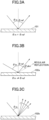
FIG 3A to FIG. 3C show reflection modes on thereflective surface 105 of theelectromagnetic wave reflector 10. InFIG. 3A , the electromagnetic wave incident onto thenormal reflector 101 is reflected at the angle of reflection θref the same as the angle of incident θin. - In
FIG. 3B , the electromagnetic wave incident onto the meta-reflector 102a is reflected at an angle of reflection θref different from the angle of incidence θin. The absolute value of the difference between the angle of reflection θref at the meta-reflector 102 and the angle of reflection by specular reflection may be called an anomalous angle θabn. As has been described above, metal patches sufficiently smaller than the operating wavelength are formed on the surface of the meta-reflector 102a to produce a surface impedance so as to control the reflection phase distribution, thereby reflecting the incident electromagnetic wave into a desired direction. For the application of theelectromagnetic wave reflector 10 to theelongated production line 3, it is desirable to guide the radio wave from the base station BS to the wireless transceiver unit WT of the equipment in theproduction line 3 at an angle of reflection θref smaller than the angle of incidence θin, as illustrated inFIG. 3B . The reason for this will be described later. - The electromagnetic wave reflected by the meta-reflector is not always a plane wave with a single angle of reflection. The incident electromagnetic wave may be diffused in a plurality of directions at different angles of reflection θref, as shown in
FIG. 3C , by well-designing the surface impedance produced on the surface of the meta-reflector 102b. A technique for achieving the reflection shown inFIG. 3C is described in, for example, PHYSICAL REVIEW B 97, "ARBITRARY BEAM CONTROL USING LOSSLESS METASURFACES ENABLED BY ORTHOGONALLY POLARIZED CUSTOM SURFACE WAVES". The intensity of the diffused electromagnetic wave may be uniform, or may have a predetermined intensity distribution according to the diffusion angle. - A plurality of
electromagnetic wave reflectors 10 may be arranged along theproduction line 3. The electromagnetic wave reflector may be used as a guard fence for safety as long as the communication quality between the base station BS and the equipment in theproduction line 3 is maintained. Prior to describing the optimal placement of the base station BS with respect to theproduction line 3, detailed configurations of theelectromagnetic wave reflector 10 are described below. - Prior to describing the optimal position of the base station BS with respect to the
production line 3, the detailed structure of theelectromagnetic wave reflector 10 is described below. -
FIG. 4 is a diagram showing the basic concept of theelectromagnetic wave reflector 10 according to the embodiment. Theelectromagnetic wave reflector 10 is placed upright on the XY plane in which the production line is provided. The height direction of theelectromagnetic wave reflector 10 is the Z direction. Theelectromagnetic wave reflector 10 has apanel 13, which has areflective surface 105 configured to reflect radio waves of a desired frequency band ranging from 1 GHz to 170 GHz, and asupport body 11 that supports thepanel 13. - The
reflective surface 105 of thepanel 13 reflects electromagnetic waves in a desired direction. Thereflective surface 105 is formed of one or both of anormal reflector 101 that provides regular reflection, andmeta reflector 102 having an artificial surface that regulates the reflection characteristics of the incident electromagnetic waves. Thenormal reflector 101 may include a reflective surface made of an inorganic conductive material or a conductive polymeric material. - Any material, any surface shape, any manufacturing process may be employed to form the meta-
reflector 102, as long as the incident electromagnetic waves can be reflected to a desired direction or diffused at a desired angular distribution. In general, a metasurface is fabricated by forming metal patches, which are sufficiently smaller than the operating wavelength, over the surface of a conductor such as a metal surface, via a dielectric layer between them. The meta-reflector 102 can be arranged at any position on thereflective surface 105, depending on which direction the electromagnetic wave is to be reflected. - The size of the
panel 13 can be appropriately designed according to the environment in which theelectromagnetic wave reflector 10 is installed. Thepanel 13 has, for example, a width of 0.5 m to 3.0 m, a height of 1.0 m to 2.5 m, and a thickness of 3.0 mm to 9.0 mm. In order for facilitating transportation and installation into the factory and simplifying the assembling, the dimensions of thepanel 13 may be about 1.4 m x 1.8 m x 5.0 mm in width x height x thickness. A part of thepanel 13 may be transparent to visible light. - The
panel 13 is held by thesupport body 11 so that theelectromagnetic wave reflector 10 can stand independently. The mechanical structure of thesupport body 11 may be of any structure as long as thepanel 13 can stably stand up with respect to the installation surface (for example, the XY plane). A plurality ofelectromagnetic wave reflectors 10 may be connected in actual use, as will be described later. The height of theelectromagnetic wave reflector 10 as a whole including thepanel 13 and thesupport body 11 is, for example, 1.5 m to 2.5 m, and it may be set to about 2.0 m from the installation surface. - In addition to the mechanical design to support and set the
panel 13 upright, thesupport body 11 has anelectrical connector part 15 to keep the electric potential of the reflection having occurred on thereflective surface 105 of thepanel 13 continuous. With the configuration of multipleelectromagnetic wave reflectors 10 connected, if the current flow induced by the incident electromagnetic waves (which is called a reflected current wave) is interrupted between thepanels 13 of adjacentelectromagnetic wave reflectors 10, the energy of the reflected electromagnetic waves is attenuated or radiated in unwanted directions, and consequently, the quality of wireless communication will deteriorate. - In order to ensure the continuity of the reflected current waves between the adjacent panels, it is desirable that the reference potential for reflection is transmitted from one panel to the other panel through the
support body 11 at a high frequency such that the reference potential is shared between the panels in a high frequency manner. It is also desirable that the continuity of the reflected current wave is as uniform as possible in the connector area of thesupport body 11. This configuration of the support body to propagate the reference potential of reflection having occurred on the reflective surface of the panel may be rephrased as a configuration to "refer to" the reference potential. - In order to allow the
electrical connector part 15 of thesupport body 11 to propagate the reference potential from one panel to the other so that the reference potential is shared between the panels, some ingenuity such as edge processing of thepanel 13 or reduction of the influence on the reflection characteristics is desired. The "edge" of thepanel 13 is an end face that connects two opposing major surfaces. Specific configurations of the electrical connector part will be described later with reference toFIG. 7 to FIG. 9D. -
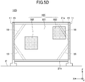
FIG. 5A to FIG. 5D show alterations of theelectromagnetic wave reflector 10. The plane on which theelectromagnetic wave reflector 10 is installed is labelled as "P". In theelectromagnetic wave reflector 10A ofFIG. 5A , a meta-reflector 102 is movably provided. Any configuration for making the meta-reflector 102 movable on thereflective surface 105 may be employed as long as undesirable interference is suppressed between the meta-reflector 102 and thereflective surface 105. For example, arod 16 holding the meta-reflector 102 may be attached to thepanel 13 so as to be slidable in the horizontal direction, and the meta-reflector 102 may be held on therod 16 so as to be vertically movable along therod 16. - The
rod 16 may be made of a non-metallic material with a low dielectric constant so as not to interfere with the reflection characteristics of thenormal reflector 101 or the meta-reflector 102. Therod 16 may be designed so that the optical interface and mechanical interference are minimized at the panel surface. The meta-reflector 102 can be moved to the optimum position on thepanel 13 according to the actual environment where theelectromagnetic wave reflector 10 is installed, or the positional relationship with respect to the base station BS. Thesupport body 11 has anelectrical connector part 15 inside, as illustrated inFIG. 4 . -
FIG. 5B shows anelectromagnetic wave reflector 10B, in which abrace 19 is provided on the back surface of thepanel 13, opposite to thereflective surface 105, to reinforce or increase the rigidity of thepanel 13 of theelectromagnetic wave reflector 10B. Thebrace 19 may be bridged between thesupport bodies 11 holding opposite edges of thepanel 13. - In an
electromagnetic wave reflector 10C ofFIG. 5C ,reinforcement beams panel 13.Reinforcement beams support bodies 11 holding the two opposed edges of thepanel 13. - In an
electromagnetic wave reflector 10D ofFIG. 5D , braces 19 are provided between the reinforcement beams 21a and 21b and between thesupport bodies 11. The above-illustrated reinforcement mechanisms can suppress the vibration mode of thepanel 13 and stabilize the electromagnetic wave reflection against the vibration of the factory floor, while the weight of the large-size panel can be reduced. InFIG. 5B to FIG. 5D , theelectrical connector part 15 for propagating the reference potential of reflection is provided inside thesupport bodies 11, as has been described in connection withFIG. 4 . - The alterations of
FIG. 5A to FIG. 5D can be combined with each other. For example, with thepanel 13 having the configuration ofFIG. 5A , the meta-reflector 102 may be held in a movable manner on thereflective surface 105, while thebrace 19 ofFIG. 5B may be provided on the back surface opposite to thereflective surface 105. -
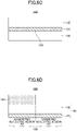
FIG. 6A to FIG. 6D show configuration examples of thereflective surface 105. Thereflective surface 105 may employ any configurations as long as it can reflect electromagnetic waves of 1 GHz to 170 GHz. For example, thereflective surface 105 can be formed of a mesh conductor, a conductive film, or a combination of a transparent resin and a conductive film, which is designed to reflect electromagnetic waves of a desired frequency band in the range from 1 GHz to 170 GHz. - By designing the
reflective surface 105 to reflect radio waves of a desired frequency band from 1 GHz to 170 GHz, a wide range of communication bands can be covered, including 1.5 GHz band and 2.5 GHz band currently used in Japan as the main frequency bands of mobile communications, and 4.5 GHz band and 28 GHz band scheduled for the next-generation 5G mobile communications network. In foreign countries, 2.5 GHz band, 3.5 GHz band, 4.5 GHz band, 24 to 28 GHz band, and 39 GHz band are planned for the 5G frequency band. The electromagnetic wave reflector of the embodiment is capable of dealing with these frequency bands, as well as 52.6 GHz band which is the upper limit of the 5G standardized millimeter wave band. - On the other hand, frequencies above 170 GHz are unlikely to be practically used for smart factories at this stage. If in the future indoor mobile communication using a terahertz band is put into practical use, the reflection band of the
reflective surface 105 may be expanded to the terahertz band by applying a photonic crystal technology. - In
FIG. 6A , apanel 13A has areflective surface 105 made of aconductor 131. Theconductor 131 is not necessarily a homogeneous conductor film, as long as it can reflect 30% or more of radio waves of 1 GHz to 170 GHz. The conductor may be formed into a mesh, a grating, or an array of holes that has a desired density suitable to reflect the electromagnetic waves of a predetermined frequency band within the above-described range. The pitch or the period of the repetition of the conductive pattern formed at the desired density may be uniform or nonuniform. The period or the average period of the conductive pattern is preferably 1/5 or less, more preferably 1/10 or less of the free-space wavelength of the selected frequency band. - The opening diameter of a typical wire mesh fence generally used in factories and warehouses is 3.2 cm, 4 cm, or 5 cm. Most of the electromagnetic waves of 1 GHz to 170 GHz pass through the typical wire mesh fence. Even if the electromagnetic waves of 1 GHz to several GHz is slightly reflected from the wire mesh fence, most of the electromagnetic waves are transmitted through the wire mesh in higher frequency bands. Such a typical wire mesh fence cannot be used as a reflector for providing stable reflection to improve the communication environment.
- In
FIG. 6B , apanel 13B is a normal reflector, and has a laminated structure of aconductor 131 and a dielectric 132 transparent to the operating frequency. Either surface of theconductor 131 can be thereflective surface 105. If electromagnetic waves are incident from theconductor 131 side, the interface between theconductor 131 and air is thereflective surface 105. If electromagnetic waves are incident from the dielectric 132 side, the interface between theconductor 131 and the dielectric 132 is thereflective surface 105. - The dielectric 132 which retains or covers the
conductor 131 preferably has a rigidity sufficient to withstand vibration, and satisfies the safety requirements of ISO 014120 provided by the international organization for standardization. Because of the use in a factory, a dielectric material is preferably transparent to visible light, while being capable of withstanding against impact due to collision with a product or a part of the manufacturing apparatus. Such materials include, but are not limited to an optical plastic, a reinforced plastic, and a reinforced glass having a predetermined mechanical strength. Examples of the optical plastic include, but are not limited to polycarbonate (PC), polymethylmethacrylate (PMMA), and polystyrene (PS). - In
FIG. 6C , apanel 13C has aconductor 131 provided betweendielectrics reflective surface 105. The rigidity required for thedielectrics FIG. 6B . - In
FIG. 6D , apanel 13D may have a meta-reflector 102 which is partially provided on the laminate ofFIG. 6B . The laminate of theconductor 131 and the dielectric 132 can be used as anormal reflector 101. The meta-reflector 102 may be fixed to the surface of the dielectric 132 of thenormal reflector 101 by lamination or other suitable processes. A region of the three-layer structure of theconductor 131, the dielectric 132, and the meta-reflector 102 is denoted as asymmetric reflective region AS which provides a metasurface. The region of the two-layer structure of theconductor 131 and the dielectric 132, without the meta-reflector 102, is denoted as the symmetric reflective region SY which provides specular reflection. - In the example of
FIG. 6D , the meta-reflector 102 is integrated with thenormal reflector 101 onto thepanel 13D as shown inFIG. 4 . The meta-reflector 102 may be configured so as to be separable from thenormal reflector 101. With the separable configuration, a movable meta-reflector 102 illustrated inFIG. 5A may be used. The position of the meta-reflector 102 on thepanel 13 may be determined according to the applied environment to adjust the position of the asymmetric reflective region AS. - As shown in
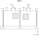
FIG. 7 , a plurality ofelectromagnetic wave reflectors 10 may be connected bysupport bodies 11 and raised on the plane P. For example, in connecting the electromagnetic wave reflectors 10-1 and 10-2, the panel 13-1 and the panel 13-2 are connected through theelectrical connector part 15 of thesupport body 11 so that the reflection potential surface is continuous between the panels. As has been described above, thesupport body 11 has both a mechanical strength to couple thepanels 13 and an electrical connectivity to achieve continuity of the reflection reference potential between thepanels 13. Configuration examples of theelectrical connector part 15 are illustrated below. -
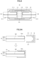
FIG. 8 shows an example of theelectrical connector part 15 of thesupport body 11 in a cross-sectional view taken along a horizontal plane when theelectromagnetic wave reflector 10 stands up on the plane P (seeFIG. 7 ). Theelectrical connector part 15 is designed to propagate the reference potential of reflection from one panel to the adjacent panel so that the reference potential of the reflection phenomenon is shared between theadjacent panels 13. - The
support body 11 has aframe 111, and anelectrical connector part 15 provided to theframe 111 to share the potential surface of reflection between thepanels 13. Theelectrical connector part 15 may have any configuration as long as it can propagate and share the reference potential of reflection between the adjacent panels 13-1 and 13-2 (which may be collectively referred to as "panels 13") in a stable manner. Theframe 111 may have any configuration as long as it is strong enough to stably hold theelectrical connector part 15. With the configuration ofFIG. 8 , theframe 111 may be made of an electrically insulating material. - In the example of
FIG. 8 , theelectrical connector part 15 includes conductive edge jackets 17-1 and 17-2 (which may be collectively referred to as "edge jackets 17") that receive the edges of thepanels 13, andbridge electrodes 112 electrically connecting theedge jackets 17 to the adjacent panels. Thebridge electrode 112 is an example of a conductive bridge that bridges the potential surfaces of the panels 13-1 and 13-2. The edge jacket 17-1 gripping the edge of the panel 13-1 and the edge jacket 17-1 gripping the edge of the panel 13-2 are electrically connected to each other by thebridge electrodes 112. Thebridge electrodes 112 are in surface contact with the edge jackets 17-1 and 17-2 to ensure the electrical connection. Upon reflection current waves occurring at the panel 13-1, the reflection current flows from the edge jacket 17-1 through thebridge electrode 112 to the edge jacket 17-2, and eventually flows into theconductor 131 of the panel 13-1. The reflection current flows through a short current path with little detour, and therefore, the reflection performance is satisfactory. - An appropriate range of the reflected current can be determined using general-purpose three-dimensional electromagnetic field simulation software, by causing a plane wave to be incident onto a model including the
connector part 15, analyzing the scattering cross section as a reflection characteristic, and determining a current path from the current distribution at the cross section. Solutions for the three-dimensional electromagnetic field simulation include the FDTD method, the finite element method, and the moment method. It is desirable that the current path is 50 times or less, preferably 10 times or less, more preferably 5 times or less, and still more preferably 2 times or less the linear distance between the panels. - The corners of the conductive material of the
electrical connector part 15, e.g., thebridge electrode 112 or ametal layer 121 which will be described in the following modification example, may be chamfered with a predetermined radius of curvature R to reduce and stabilize the scattering at the edges of the conductor material. The radius of curvature R of the chamfered part is at least 1 mm, preferably 2 mm or more, more preferably 4 mm or more, and even more preferably 8 mm or more. - The
frame 111 is provided so as to ensure the strength of thesupport body 11. Preferably, theframe 111 is formed of an insulating elastic material or a resin so as to suppress the shunting of the reflected current. The above-described preferred dimensional ranges also apply the following modification examples. -
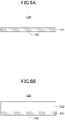
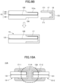
FIG. 9A andFIG. 9B show examples of edge processing of thepanel 13. InFIG. 9A , thepanel 13 has aconductor 131, which is provided betweendielectrics reflective surface 105. Theedge jacket 17 may be a conductive rail with an open square or U-shaped cross-section, which has a pair ofouter surfaces 171 and abottom face 172 connecting theouter surfaces 171. Aconductive adhesive 18 such as a silver paste may be applied in advance to the inner surface of theedge jacket 17. - The
conductor 131 may be folded back at the edge of thepanel 13 and drawn out to either one of the dielectric surfaces. Upon insertion of the edge of thepanel 13 into theedge jacket 17, the foldedpart 131a of theconductor 131 comes into surface contact with the inner wall of theedge jacket 17. By drawing out theconductor 131 so as to cover a part of the surface of thepanel 13 at the foldedpart 131a, the contact area between theconductor 131 and theedge jacket 17 is increased and electrical connection becomes stable. - The thickness of a part of the
dielectrics panel 13 so as to form acutout 134, as shown inFIG. 9B . The edge part thinned by thecutout 134 can be fit into theedge jacket 17. With this configuration, theouter surface 171 of the edge jacket aligns with the surface of thepanel 13, which facilitates handling of thepanel 13. -
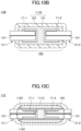
FIG. 10A to FIG. 10E show modifications of theelectrical connector part 15 of thesupport body 11. InFIG. 10A , thesupport body 11A has aframe 111A made of a carbon-containing material, in place of the insulatingframe 111. Anelectrical connector part 15A is formed by theframe 111A and the edge jackets 17-1 and 17-2. Carbon Fiber Reinforced Plastics (CFRP) can be used as the carbon-containing material. By combining carbon fiber and resin, the carbon fiber, which is a conductor, and the resin, which is an insulator, can be integrally molded using a process such as continuous pultrusion molding, and high strength can be achieved. - The CFRP, which holds the edge jackets 17-1 and 17-2, serves by itself as the
electrical connector part 15A. Electrical connection can be established between the edge jackets 17-1 and 17-2 without using abridge electrode 112. Regarding the reflective property, carbon fiber has better reflective performance than bulk metal, and the reflective characteristics of theframe 111A can be improved. - From the viewpoint of achieving both reflective performance and mechanical strength, it is preferable that the carbon fiber content ratio of CFRP is 50% or more, 60% or more, 70% or more, 80% or more, or even 90% or more. On the other hand, the resin content ratio of CFRP is preferably 50% or less, 40% or less, 30% or less, 20% or less, or even 10% or less.
- In
FIG. 10B , asupport body 11B has aframe 111B formed of a laminate of ametal layer 121 and aresin layer 122. Themetal layer 121 couples the panels 13-1 and 13-2, while covering the outer surfaces of the edge jackets 17-1 and 17-2. Themetal layer 121 being in contact with the edge jackets 17-1 and 17-2 serves as theelectrical connector part 15B. Theresin layer 122 enhances from the outside the connection between the panels through themetal layer 121. An adhesive may be used for the enhancement (i.e., the resin layer 122). Such an adhesive may be an acrylic adhesive or an epoxy adhesive. This configuration can suppress unwanted sneak current. The configuration with the combination of themetal layer 121 and theresin layer 122 can facilitate the design and fabrication of theframe 111B. The strength of theframe 111B is also guaranteed by covering themetal layer 121 with theresin layer 122 in the laminating direction. -
FIG. 10C shows a configuration that connects the edge-processedpanels 13 of FIG. 8B. The surface of thepanel 13 and the outer surface of theedge jacket 17 are aligned, and accordingly, thepanel 13 fit into theedge jacket 17 in advance can be inserted into theframe 111C. Theframe 111C is made of, for example, an insulating plastic. At theelectrical connector part 15C, the electric current produced by reflection of the incident electromagnetic wave flows from theedge jacket 17 through thebridge electrode 112C into theconductor 131 of theadjacent panel 13 by a short current path. Thebridge electrode 112C may be sufficiently wide to ensure the surface contact with the entirety of the outer surface of the edge jackets 17-1 and 17-2. Upon reflection of the incident electromagnetic waves by the panel 13-1, a highfrequency current flows through at least a part of thebridge electrode 112C to theconductor 131 of the panel 13-2 as indicated by the white arrow, with less sneak current. -
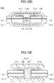
FIG. 10D shows a configuration of anelectrical connector part 15D of asupport body 11D. Theelectrical connector part 15D has abridge electrode 114 that electrically connects the edge jackets 17-1 and 17-2. Thebridge electrode 114 connects the bottom surfaces 172 of the edge jackets 17-1 and 17-2. The configuration ofFIG. 10D is advantageous in that the high frequency current can flow in the shortest path from the conductor 131-1 to the along the shortest path through the edge jacket 17-1, thebridge electrode 114, the edge jacket 17-2, and the conductor 131-2. Although, in the example ofFIG. 10D , thebridge electrode 114 connects part of the bottom surfaces 172 of the edge jackets 17-1 and 17-2, the thickness of thebridge electrode 114 can be increased so that the edge jackets 17-1 and 17-2 are connected at the entirety of the bottom surfaces 172. By thickening thebridge electrode 114, the electrical connection and the physical connection become more stable. By enclosing the periphery of thebridge electrode 114 with an insulatingframe 111D, the mechanical strength of theelectrical connector part 15D is improved, and the reliability of the electrical connection is ensured. -
FIG. 10E shows a configuration using aframe 111E of a composite type of metal and resin. Theframe 111E has ametal connector 141 and aresin reinforcement 142 that covers themetal connector 141. Themetal connector 141 can be easily manufactured by extrusion molding or the like, and the connector itself has a certain degree of strength while ensuring electrical connection. By covering the metal connector with theresin reinforcement 142, themetal connector 141 and theresin reinforcement 142 together achieve the strength as the supporting member. Theresin reinforcement 142 may be formed of an adhesive such as an acrylic adhesive or an epoxy adhesive, thereby reducing the thickness of themetal connector 141 and suppressing residual inductance caused by current detours. The corners may be rounded to prevent diffraction at the corners. -
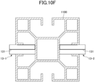
FIG. 10F shows a structure using a commerciallyavailable frame 1100 formed by extrusion molding of aluminum as a reference example. With theframe 1100 having a complicated cross-sectional shape, currents flow in various directions, and residual inductance and stray capacitance are generated due to the complicated current detour paths. The response varies in a complicated manner, depending on the incident electromagnetic waves, and the sharing or propagation of the reference potential of reflection is adversely affected. For these reasons, it is preferable to adopt the configurations of theelectrical connector part 15 shown inFIG. 8 andFIG. 10A toFIG. 10E for theframe body 11. -
FIG. 11A shows connection of the electromagnetic wave reflectors 10-1 and 10-2. Edge jackets 17-1 are provided on both edges of the panel 13-1. Edge jackets 17-2 are provided on both edges of the panel 13-2. The panel 13-1 and the panel 13-2 are fit into the edge jackets 17-1 and 17-2, respectively, in advance, and are connected by thesupport body 11. - The
support body 11 may have aframe 111 with anelectrical connector part 15 and aguide beam 118 for receiving theframe 111. Theframe 111 and theguide beam 118 may be formed separately, as illustrated inFIG. 11A , or alternatively, they may be integrated into one unit. Upon receiving the panels 13-1 and 13-2 by theframe 111 from both sides, thebridge electrode 112 of theelectrical connector part 15 comes into contact with the outer surfaces of the edge jackets 17-1 and 17-2 of the panels 13-1 and 13-2, and electrical connection is established between the reflective surfaces 105-1 and 105-2 of the electromagnetic wave reflecting devices 10-1 and 10-2. - By fitting the
frame 111 for connecting the panels 13-1 and 13-2 to theguide beam 118, theframe 111 and theguide beam 118 are combined to form thesupport body 11 to couple the panels 13-1 and 13-2. -
FIG. 11B shows the state of theelectromagnetic wave reflectors 10 before connection. For each of the electromagnetic wave reflectors 10-1 to 10-3, aframe 111 having anelectrical connector part 15 is attached in advance to one of the side edges of thepanel 13, and aguide beam 118 is attached to the other side edge. Thereflective surfaces 105 of the electromagnetic wave reflector 10-1 to 10-3 may have any configuration shown inFIG. 6A to FIG. 6D . - The
frame 111 is configured to be adaptable to theguide beam 118 attached to anotherelectromagnetic wave reflector 10, while theguide beam 118 is configured to be able to receive theframe 111 attached to anotherelectromagnetic wave reflector 10. For instance, theguide beam 118 of the electromagnetic wave reflector 10-1 receives theframe 111 of the electromagnetic wave reflector 10-2. Theguide beam 118 of the electromagnetic wave reflector 10-2 receives theframe 111 of the electromagnetic wave reflector 10-3. By combining multipleelectromagnetic wave reflectors 10 of a standard size, the length of the production line can be covered in a flexible manner. The assembly work may be carried out on-site in the factory. The individual electromagnetic wave reflectors 10-1 to 10-3 are simple in configuration and easy to transport. -
FIG. 11C shows the state of theelectromagnetic wave reflectors 10 after connection. Theframe 111, together with the guide beams 118, form thesupport body 11. A plurality of electromagnetic wave reflectors 10-1, 10-2, and 10-3 can be connected by thesupport body 11 to form an electromagnetic wavereflective fence 100. Theelectrical connector part 15 of theframe 111 can suppress discontinuity of the reflected current waves at the boundary between thepanels 13. - A base 119 may be provided in advance to one or both of the
guide beam 118 and theframe 111, thereby allowing the connected electromagnetic wave reflectors 10-1 to 10-3 to stand up by themselves on the installation plane. Acover 29 may be provided to the edge of thelast panel 13 of the electromagnetic wave reflector 10-3 at the end position to protect theedge jacket 17 and theguide beam 118. -
FIG. 12 andFIG. 13 show a mechanism that reinforces the connections of a plurality of electromagnetic wave reflectors 10-1 and 10-2. InFIG. 12 , (A) is a front view of the electromagnetic wavereflective fence 100, (B) is a side view before the reinforcingmechanism 125 is tightened, and (C) is a side view after the reinforcingmechanism 125 is tightened.FIG. 13 shows a configuration example of thereinforcement mechanism 125.FIG. 13 shows a front view ofguide grooves 129 formed in an attachingsurface 127a of acover 127 of thereinforcement mechanism 125, and cross-sectional views taken along the cross-sections A and B of the front view. Thecover 127 is attached to thepanels 13 at the attachingsurface 127a. - In order to improve the connection strength and electrical connectivity, the
reinforcement mechanism 125 shown inFIG. 12 andFIG. 13 can be used as necessary unless the reflection characteristics are deteriorated. Apin 128 is passed through ahole 126 formed in thepanel 13, and thecover 127 is attached to the surface of thepanel 13 opposite to the reflective surface. By moving thepin 128 along theguide groove 129 formed in the attachingsurface 127a of the cover 127 (transition from the position of cross section A to the position of cross section B), thepanel 13 can be pressed against thesupport body 11 from both sides. By the tightening of thereinforcement mechanism 125, the position of thehole 126 formed in thepanel 13 slightly shifts towards thesupport body 11. The elastic force of thepanel 13 enhances the connection between the edge of thepanel 13 and theelectrical connector part 15 of the support body 11 (seeFIG. 17 ). - The mechanism for reinforcing the connection between multiple
electromagnetic wave reflectors 10 is not limited to the above-described example shown inFIG. 12 andFIG. 13 , and other appropriate mechanisms including a fastener and a ratchet may be used unless the electromagnetic wave reflection characteristics are impaired. The design of theedge jacket 17 and theelectrical connector part 15 may be appropriately modified assuming the above-described pressure contact process. -
FIG. 14 shows the size of the meta-reflector 102, assuming that a transmitter "Tx" and a receiver "Rx" are used. The transmitter Tx is, for example, a base station BS. Receiver Rx is, for example, equipment located in theproduction line 3. The distance from the transmitter Tx to thesurface 102s of the meta-reflector 102 is denoted as d1, and the distance from thesurface 102s of the meta-reflector 102 to the receiver Rx is denoted as d2. - Given an application to a production line, the total distance D of d1 and d2 is, for example, 40 m (D=d1+d2=40 m). The standard length of the production line is 80 m. Assuming that the base stations BS are positioned at both ends of the production line in the length direction, and that the two base stations BS provide a standard rectangular service area, then the total length distance D is estimated to be 40 m (D=40 m).
- The radius R of the first Fresnel zone is defined by Formula (1) when the radio waves emitted from the transmitter Tx and reflected from the meta-
reflector 102 reach the receiver Rx in phase.
-
FIG. 15 shows specific examples of the radius R of the first Fresnel zone derived from Formula (1). When the operating frequency is 28 GHz, d1 is 30 m, and d2 is 10 m, then the radius R of the first Fresnel zone is 0.283 m. At the same frequency, with d1 of 35 m and d2 of 5 m, the radius R is 0.216 m. - When the operating frequency is 3.8 GHz, d1 is 30 m, and d2 is 10 m, then the radius R of the first Fresnel zone is 0.770 m. At the same frequency, with d1 of 35 m and d2 of 5 m, the radius R is 0.588 m.
- It is desirable for the equipment M used in the production line to be able to receive the reflected wave from the
electromagnetic wave reflector 10 in phase with the direct wave from the base station BS from the viewpoint of improving the received power. In the application of theelectromagnetic wave reflector 10 having one or more meta-reflectors 102 to a production line, the minimum size of one meta-reflector 102 is 0.5 meters per side or more for the 28 GHz band, considering the first Fresnel zone that allows in-phase signal reception. For the 3.8 GHz band, the minimum size of one meta-reflector 102 is preferably about 1 meter per side. - With the configuration of multiple meta-
reflectors 102 applied to onepanel 13 as illustrated inFIG. 5B to FIG. 5D , it is preferable for each of the meta-reflectors 102 to cover at least the first Fresnel zone. - The similar estimation applies to the
normal reflector 101 because the radius R of the first Fresnel zone does not depend on the relationship between the angle of incidence and the angle of reflection. In order to guide the radio waves incident onto thenormal reflector 101 to the receiver Rx, while maintaining the same phase by regular reflection, the size of thenormal reflector 101 is desirably 50 centimeters per side. - If the meta-
reflector 102 is used in a production line covered by a service area with a large aspect ratio, the oblique angle of either incidence or reflection becomes deep. So, the layout and the positional relationship among theproduction line 3, the base station BS, and theelectromagnetic wave reflector 10 will be discussed below. - The layout of the
wireless transmission system 1 will be described with reference toFIGs. 16A, 16B ,17A , and17B . As has been described with reference toFIG. 1 andFIG. 2 , thewireless transmission system 1 includes a base station BS, which transmits and receives radio waves in the frequency band of 1 GHz to 170 GHz, aproduction line 3 in which manufacturing equipment capable of transmitting and receiving the radio waves is placed, and anelectromagnetic wave reflector 10 provided along at least a part of the production line. Theelectromagnetic wave reflector 10 has areflective surface 105 that reflects the radio waves of the above-described frequency band. - The base station BS is preferably positioned closer to the
production line 3 than to the line L horizontally extending from thereflective surface 105, as will be described in more detail below. For instance, the base stations BS may be arranged at both ends of theelongated production line 3. The manufacturing equipment in theproduction line 3 can telecommunicate with the base station BS directly or via theelectromagnetic wave reflector 10 in the above-described frequency band. -
FIG. 16A showsPattern 1 of reflection in thewireless transmission system 1. InPattern 1, the base stations BS and theproduction line 3 are provided in such a positional relationship that the radio waves emitted from the base station BS are incident onto thereflective surface 105 at a deep angle with respect to the normal to thereflective surface 105 of theelectromagnetic wave reflector 10 and reflected at a shallow angle, as indicated by the solid arrows. In other words, the radio wave is incident onto thereflective surface 105 at an angle greater than or equal to 45 degrees, and is reflected at an angle smaller than the angle of regular reflection. - In order to allow the radio waves from the base station BS to be incident on the
reflective surface 105 at a deep angle, the base station BS is preferably positioned closer to theproduction line 3 than to the Line L horizontally extending from the surface of theelectromagnetic wave reflector 10, and is preferably located at both ends of theelongated production line 3. By allowing the radio waves to be incident onto thereflective surface 105 at a deep angle, the radio waves can be guided to the center area of theproduction line 3. -
FIG. 16B showsPattern 2 of reflection. Inpattern 2, the base stations BS and theproduction line 3 are laid in such a positional relationship that the radio waves emitted from the base stations BS are incident onto thereflective surface 105 at a shallow angle with respect to the normal to thereflective surface 105 and are reflected at an angle deeper than the incident angle. In other words, inPattern 2, the radio waves are incident onto thereflective surface 105 at an angle of incidence of 45 degrees or less, and are reflected at an angle greater than the regular reflection. - In
Pattern 2, the base stations BS are positioned closer to theproduction line 3 than to the Line L horizontally extending from thereflective surface 105 of theelectromagnetic wave reflector 10, but are positioned closer to the center, rather than the ends, of theproduction line 3 in the longitudinal direction.Pattern 2 is more sensitive to variations in the oblique incidence angle, as will be explained below. -
FIG. 17A shows the baseline robustness ofPattern 1, and FIG. 31B shows the baseline robustness ofPattern 2. The baseline robustness means the stability of the angle of reflection when the angle of incidence is changed by 1 degree. The baseline robustness is high if the change in the reflection angle is small with respect to the change in the incident angle of 1 degree. - In
FIG. 17A forPattern 1, the anomalous angle θabn is changed to 7 different angles, namely 20°, 25°, 30°, 35°, 40°, 45°, and 50°, to estimate the fluctuation in the reflection angle with respect to the change in the incident angle. The fluctuation in the reflection angle is almost the same at the seven different anomalous angles θabn, and accordingly, the plotted lines overlap each other, which appear as one thick line in the figure. - The anomalous angle θabn is the difference between the reflection angle of regular reflection and the reflection angle of asymmetric reflection in which radio waves are reflected at an angle different from the incident angle, as has been described with reference to
FIG. 3B . Varying the anomalous angle θabn from 20° to 50° corresponds to controlling the direction of asymmetric reflection over an angular range of 30°. - In the range of the incident angle from 50° to 75° (deep incidence), the fluctuation of the reflection angle with respect to the change of the incident angle of 1 degree is as small as less than 1 degree, and is almost constant regardless of the incident angle. When the incident angle is deep, the reflection controllability in the asymmetric reflection is high. It is easily inferred that the tendency of FIG. 31A exhibiting little fluctuation in the reflection angle can be maintained even at an incident angle exceeding 75° and approaching 90°.
- In
FIG. 17B forPattern 2, the anomalous angle θabn is changed to seven different angles, namely 20°, 25°, 30°, 35°, 40°, 45°, and 50° to estimate the fluctuation in the reflection angle with respect to the change in the incident angle. In the range of the incident angle from 15° to 40° (shallow incidence), the fluctuation in the reflection angle with respect to the 1 degree change in the incident angle varies depending on the incident angle, and also varies greatly depending on the anomalous angle θabn. - With a small anomalous angle θabn, that is, with a small difference from the angle of regular reflection, the incidence angle dependence of the fluctuation in the reflection angle is small. As the anomalous angle θabn increases, that is, as the directional change of reflection by the meta-
reflector 102 increases, the fluctuation in the angle of reflection with respect to the 1 degree change of the incident angle becomes very large, and the amount of fluctuation in the angle of reflection also varies greatly depending on the angle of incidence. In the shallow range of the incident angle of 15° to 40°, the controllability in the asymmetric reflection is not satisfactory. - From
FIG. 17A andFIG. 17B , when base stations BS are introduced in theproduction line 3, the base stations BS are preferably located so that the incident angle of the radio waves emitted from the base stations BS and incident onto theelectromagnetic wave reflector 10 is 50° or greater, from the viewpoint of suppressing the fluctuation of the reflection angle depending on the incident angle. Therefore, the layout shown inFIG. 17A is preferable to the layout ofFIG. 16B . -
FIG. 18 shows quantification of the baseline robustness. The baseline robustness ofFIG. 17A andFIG. 17B can be estimated by the following procedure. A phase jump Φ(x) is determined by inputting a certain incident angle θi and a reflection angle θr to a function f for calculating a phase jump distribution, where x denotes the position in the x-direction on the reflective surface. A phase jump represents the amount of phase to be added to a reflected wave to guide the reflected wave to a desired direction. The phase jump distribution dΦ/dx is expressed as
- Using a surface impedance Zs and a wave impedance η described in PHYSICAL REVIEW B 94.075142 (2016), V.S. Asadchy, et al., "PERFECT CONTROL OF REFLECTION AND REFRACTION USING SPATIALLY DISPERSIVE METASURFACES", the function f for determining phase jump distribution Φ(x) is expressed by the following formula.

- The surface impedance Zs(x) is expressed by the following formula.

- Next, the incident angle is incremented by 1 degree, and another phase jump Φ'(x) is calculated from the phase jump distribution function f by inputting the new incident angle and the corresponding (reflection angle)'.
- Then, the (reflection angle)' that minimizes Φ'(x)-Φ(x) is determined, which is regarded as the fluctuation of the reflection angle with respect to the change in the incident angle.
FIG. 17A andFIG. 17B are plots of the calculated fluctuation of the reflection angle as a function of the angle of incidence. -
FIG. 19A shows changes in phase jumps ofPattern 1. The horizontal axis represents the position (m) and the vertical axis represents the phase (degrees). In Deep-in Shallow-out of FIG. 33A, the angle of reflection θr is fixed at 30 degrees, and the angle of incidence θi is changed to 68.5°, 70°, and 71.5°. At deep angles of incidence, the distribution of phase jumps does not change significantly even if the angle of incidence changes in the range of 3°. -
FIG. 19B shows changes in phase jumps ofPattern 2. The horizontal axis represents the position (m) and the vertical axis represents the phase (degrees). In Shallow-in Deep-out ofFIG. 19B , the angle of reflection θr is fixed at 60 degrees, and the angle of incidence θi is changed to 18.5°, 20°, and 21.5°. In the case of the shallow angle incidence, if the incidence angle changes in the range of 3° as inFIG. 19A , the distribution of phase jumps is greatly shifted depending on the incidence angle. - It is also understood from
FIG. 19A andFIG. 19B that the layout design ofFIG. 16A is preferable to that ofFIG. 16B in terms of equalizing the phase jump distribution of the radio waves incident onto theelectromagnetic wave reflector 10. In the layout ofFIG. 16A , the base stations BS are provided at positions where the radio waves emitted from the base stations BS are incident onto thereflective surface 105 of theelectromagnetic wave reflector 10 at an incident angle of 50 degrees or more. - Although the present invention has been described above based on specific configuration examples, various alterations and substitutions are possible without departing from the scope of the invention. The meta-
reflector 102 may adopt any configuration as long as the reflection characteristic such as the reflection phase can be controlled. A periodic structure having frequency selectivity or wavelength selectivity may be appropriately designed. In some or all of the configuration examples described above, the outer surfaces of the bridge electrodes may be coated with an insulating film. - The
electromagnetic wave reflector 10 may be provided along one side of theelongated production line 3 as shown inFIG. 16A , or it may be provided along both sides of theproduction line 3 as shown inFIG. 2 . If theproduction line 3 is L-shaped, theelectromagnetic wave reflector 10 may be installed along each region forming a rectangular area, or alternatively, theelectromagnetic wave reflector 10 may be installed in the main areas of the production line. In either case, the base station BS is provided at a position where radio waves from the base station are incident onto thereflective surface 105 of theelectromagnetic wave reflector 10 at a deep incident angle. - The equipment in the
production line 3 does not always receive only the radio waves reflected from theelectromagnetic wave reflector 10, but can receive the radio waves directly from the base station BS. In this case, receive diversity can be achieved by in-phase signal reception. If two base stations BS are provided at both ends of theelongated production line 3, cooperative type base stations may be used. - An individual
electromagnetic wave reflector 10 may be transported with theframe 111 fixed to one edge of thepanel 13 and theguide beam 118 attached to the opposing edge, as shown inFIG. 11A . In this case, on-site work for attaching parts is unnecessary, and assembly is facilitated. Alternatively, thepanel 13 may be transported with only theframe 111 attached, and assembled on site using the guide beams 118. Moreover, the metasurface may be attached onto thepanel 13 at the installation site of theelectromagnetic wave reflector 10, as illustrated inFIG. 5A . - The electromagnetic wave reflector and the wireless transmission system according to the embodiments can contribute to implementation of a smart factory.
- This international application is based upon and claims priority to earlier
Japanese Patent Application No. 2020-064578 filed March 31, 2020 -
- 1: wireless transmission system
- 3: production line
- 10, 10A-10G, 10-1, 10-2: electromagnetic wave reflector
- 11: frame body
- 13, 13-1, 13-2: panel
- 15, 15A-15E: electrical connector part
- 16: rod
- 17, 17-1, 17-2: edge jacket
- 19: brace
- 100: electromagnetic wave fence
- 101: normal reflector
- 102: meta reflector
- 105: reflective surface
- 111, 111A-111E: frame
- 112, 112A, 114: bridge electrode
- 118: guide beam
- 125: reinforcing mechanism
- 131: conductor
- 132, 133: dielectric
- BS, BS1, BS2: base station
- WT, WT1, WT2: wireless transceiver units
- SY: symmetric reflective region
- AS: asymmetric reflective region
Claims (10)
- A wireless transmission system comprising:a base station that transmits and receives a radio wave in a frequency band selected from a range of 1 GHz to 170 GHz; andan electromagnetic wave reflector having a reflective surface that reflects the radio wave and provided along at least a part of a production line in which manufacturing equipment that transmits and receives the radio wave is used.
- The wireless transmission system as claimed in claim 1,
wherein the base station is positioned closer to the production line than to a line horizontally extending from the reflective surface. - The wireless transmission system as claimed in claim 1 or 2,
wherein the electromagnetic wave reflector is provided on both sides of the production line along at least a part of the production line. - The wireless transmission system as claimed in any one of claims 1 to 3,wherein the base station includes a first base station and a second base station provided at both ends of the production line in a longitudinal direction, andwherein the manufacturing equipment is capable of communicating with at least one of the first base station and the second base station in the frequency band.
- The wireless transmission system as claimed in any one of claims 1 to 4, wherein the reflective surface has a symmetric reflective region that reflects a radio wave at a reflection angle same as an incident angle of the radio wave, and an asymmetric reflective region that reflects the radio wave at an angle different from the incident angle.
- The wireless transmission system as claimed in claim 5, wherein the incident angle of the radio wave transmitted from the base station and incident onto the asymmetric reflective region is 50° or more.
- The wireless transmission system as claimed in claim 5 or 6,
wherein an area of the asymmetric reflective region covers at least a first Fresnel zone determined by a frequency of the radio wave. - The wireless transmission system as claimed in claim 1, wherein the base station is positioned so that an incident angle of the radio wave transmitted from the base station and incident onto the reflective surface is 50° or more.
- The wireless transmission system as claimed in any one of claims 1 to 8,
wherein the reflective surface has a mesh, a grating, or an array of holes formed at a density that reflects the radio wave of the frequency band, and an average period of the mesh, the grating, or the array of holes formed at the density is one fifth (1/5) or less of a free-space wavelength of the frequency band. - The wireless transmission system as claimed in any one of claims 1 to 9, wherein a plurality of electromagnetic wave reflectors are mechanically and electrically connected.
Applications Claiming Priority (2)
| Application Number | Priority Date | Filing Date | Title |
|---|---|---|---|
| JP2020064578 | 2020-03-31 | ||
| PCT/JP2020/045592 WO2021199504A1 (en) | 2020-03-31 | 2020-12-08 | Wireless transmission system |
Publications (3)
| Publication Number | Publication Date |
|---|---|
| EP4131655A1 true EP4131655A1 (en) | 2023-02-08 |
| EP4131655A4 EP4131655A4 (en) | 2024-04-10 |
| EP4131655B1 EP4131655B1 (en) | 2025-11-19 |
Family
ID=77928893
Family Applications (1)
| Application Number | Title | Priority Date | Filing Date |
|---|---|---|---|
| EP20929502.1A Active EP4131655B1 (en) | 2020-03-31 | 2020-12-08 | Wireless transmission system |
Country Status (6)
| Country | Link |
|---|---|
| US (1) | US12308521B2 (en) |
| EP (1) | EP4131655B1 (en) |
| JP (1) | JP7548297B2 (en) |
| KR (1) | KR102799656B1 (en) |
| CN (1) | CN115349200B (en) |
| WO (1) | WO2021199504A1 (en) |
Cited By (1)
| Publication number | Priority date | Publication date | Assignee | Title |
|---|---|---|---|---|
| EP4311027A4 (en) * | 2021-03-16 | 2025-03-12 | Agc Inc. | Electromagnetic wave reflection device, electromagnetic wave reflection fence, and method for assembling electromagnetic wave reflection device |
Families Citing this family (27)
| Publication number | Priority date | Publication date | Assignee | Title |
|---|---|---|---|---|
| JP7601233B2 (en) * | 2021-08-02 | 2024-12-17 | 日本電信電話株式会社 | Wireless communication system, wireless communication system management method, wireless communication device, and control device |
| FR3128591B1 (en) * | 2021-10-27 | 2023-09-08 | Psa Automobiles Sa | REFLECTION DEVICE WITH METASURFACE(S) FOR A DEVICE FOR DETECTING IDENTIFICATION ELEMENTS |
| WO2023120137A1 (en) * | 2021-12-20 | 2023-06-29 | Agc株式会社 | Wireless transmission system and electromagnetic wave reflection apparatus |
| JPWO2023120138A1 (en) * | 2021-12-20 | 2023-06-29 | ||
| JP7816388B2 (en) * | 2022-02-07 | 2026-02-18 | Agc株式会社 | Electromagnetic wave reflecting device, electromagnetic wave reflecting fence, electromagnetic wave reflecting device installation method, and electromagnetic wave reflecting fence installation method |
| EP4525211A1 (en) | 2022-05-09 | 2025-03-19 | Agc Inc. | Electromagnetic wave reflection device and electromagnetic wave reflection fence |
| WO2023228693A1 (en) * | 2022-05-24 | 2023-11-30 | 京セラ株式会社 | Power transmission system and power transmission method |
| JPWO2023234082A1 (en) * | 2022-05-31 | 2023-12-07 | ||
| WO2023233885A1 (en) * | 2022-06-01 | 2023-12-07 | Agc株式会社 | Electromagnetic wave reflection device, electromagnetic wave reflection fence, and reflection panel |
| EP4535569A1 (en) * | 2022-06-01 | 2025-04-09 | Agc Inc. | Electromagnetic wave reflection device, electromagnetic wave reflection fence, and reflection panel |
| JPWO2023233921A1 (en) * | 2022-06-01 | 2023-12-07 | ||
| KR20250018469A (en) * | 2022-06-01 | 2025-02-06 | 에이지씨 가부시키가이샤 | Electromagnetic wave reflector, electromagnetic wave reflector fence and reflector panel |
| JP7405316B1 (en) * | 2022-06-27 | 2023-12-26 | 大日本印刷株式会社 | Reflective structure, reflective structure manufacturing method, and frequency selective reflector set |
| JPWO2024029325A1 (en) * | 2022-08-03 | 2024-02-08 | ||
| JPWO2024038682A1 (en) * | 2022-08-17 | 2024-02-22 | ||
| WO2024038775A1 (en) * | 2022-08-17 | 2024-02-22 | Agc株式会社 | Reflective panel, electromagnetic wave reflection device, and electromagnetic wave reflection fence |
| CN119768972A (en) * | 2022-09-02 | 2025-04-04 | Agc株式会社 | Electromagnetic wave reflecting device and electromagnetic wave reflecting fence |
| CN119895663A (en) * | 2022-09-26 | 2025-04-25 | Agc株式会社 | Reflection panel, electromagnetic wave reflection device using same, electromagnetic wave reflection fence, and method for manufacturing reflection panel |
| JP7727605B2 (en) * | 2022-09-27 | 2025-08-21 | Kddi株式会社 | Reflectors and reflectors |
| WO2024135455A1 (en) * | 2022-12-21 | 2024-06-27 | Agc株式会社 | Reflective panel and electromagnetic wave reflecting device |
| WO2024142434A1 (en) * | 2022-12-27 | 2024-07-04 | Agc株式会社 | Wireless transmission system |
| WO2024190085A1 (en) * | 2023-03-14 | 2024-09-19 | Agc株式会社 | Electromagnetic wave reflecting panel, electromagnetic wave reflecting device, electromagnetic wave reflecting fence, and method for manufacturing electromagnetic wave reflecting panel |
| JPWO2024241665A1 (en) * | 2023-05-23 | 2024-11-28 | ||
| WO2024247411A1 (en) * | 2023-05-29 | 2024-12-05 | Agc株式会社 | Electromagnetic wave reflection device, electromagnetic wave reflection fence, and installation method for electromagnetic wave reflection panel |
| WO2025041555A1 (en) * | 2023-08-21 | 2025-02-27 | Agc株式会社 | Electromagnetic wave reflection panel, electromagnetic wave reflection device using same, electromagnetic wave reflection fence, method for manufacturing electromagnetic wave reflection panel, and method for evaluating electromagnetic wave reflection panel |
| CN116946328B (en) * | 2023-09-20 | 2023-12-29 | 江苏锦程船舶制造有限公司 | Rescue unmanned ship |
| WO2025105137A1 (en) * | 2023-11-13 | 2025-05-22 | Agc株式会社 | Wireless transmission system |
Family Cites Families (23)
| Publication number | Priority date | Publication date | Assignee | Title |
|---|---|---|---|---|
| US6323601B1 (en) * | 2000-09-11 | 2001-11-27 | Nordson Corporation | Reflector for an ultraviolet lamp system |
| US6559460B1 (en) * | 2000-10-31 | 2003-05-06 | Nordson Corporation | Ultraviolet lamp system and methods |
| US6732451B2 (en) * | 2001-04-11 | 2004-05-11 | Intermec Ip Corp. | UV curing module for label printer |
| JP2003249872A (en) * | 2002-02-22 | 2003-09-05 | Sharp Corp | Wireless communication system |
| JP4235010B2 (en) * | 2003-02-26 | 2009-03-04 | Tdk株式会社 | Unnecessary radio wave suppression structure |
| JP4301893B2 (en) * | 2003-08-07 | 2009-07-22 | 積水樹脂株式会社 | Radio wave absorption panel |
| JP4410695B2 (en) * | 2005-02-10 | 2010-02-03 | 株式会社神戸製鋼所 | Wireless LAN system and antenna module thereof |
| JP4445883B2 (en) * | 2005-02-28 | 2010-04-07 | Necエンジニアリング株式会社 | Wireless data carrier writing / reading system |
| JP4892207B2 (en) | 2005-07-25 | 2012-03-07 | 鹿島建設株式会社 | Translucent electromagnetic wave shielding plate joining structure and joining tool |
| US7909595B2 (en) * | 2006-03-17 | 2011-03-22 | Applied Materials, Inc. | Apparatus and method for exposing a substrate to UV radiation using a reflector having both elliptical and parabolic reflective sections |
| JP4609373B2 (en) * | 2006-04-28 | 2011-01-12 | 日本電気株式会社 | RFID communication system and RFID communication method |
| JP4407720B2 (en) * | 2006-06-09 | 2010-02-03 | 日本電気株式会社 | Wireless communication system and wireless communication method |
| JP4853329B2 (en) * | 2007-02-28 | 2012-01-11 | 株式会社豊田中央研究所 | Radio wave reflector and antenna |
| US7991257B1 (en) * | 2007-05-16 | 2011-08-02 | Fusion Optix, Inc. | Method of manufacturing an optical composite |
| US9190738B2 (en) * | 2010-04-11 | 2015-11-17 | Broadcom Corporation | Projected artificial magnetic mirror |
| JP5606283B2 (en) * | 2010-11-10 | 2014-10-15 | 三菱電機株式会社 | Wireless device |
| JP2016042222A (en) * | 2014-08-14 | 2016-03-31 | 株式会社マーストーケンソリューション | RFID system for conveyor |
| CN110313137B (en) * | 2017-02-21 | 2022-06-14 | 3M创新有限公司 | Passive repeater device, microwave network and method for designing repeater device |
| US10547116B2 (en) * | 2017-08-01 | 2020-01-28 | University Of Cyprus | Wireless communication paradigm: realizing programmable wireless environments through software-controlled metasurfaces |
| US11342682B2 (en) * | 2018-05-24 | 2022-05-24 | Metawave Corporation | Frequency-selective reflector module and system |
| JP2020064578A (en) | 2018-10-15 | 2020-04-23 | 株式会社エモスタ | Sense-of-value quantification device and matching and recommendation method utilizing the same |
| WO2021199503A1 (en) | 2020-03-31 | 2021-10-07 | Agc株式会社 | Electromagnetic wave reflection device, electromagnetic wave reflection fence, and electromagnetic wave reflection device assembly method |
| CN111983560B (en) * | 2020-08-05 | 2022-12-30 | 北京理工大学 | Dual-reconfigurable intelligent surface-assisted millimeter wave single base station positioning method |
-
2020
- 2020-12-08 WO PCT/JP2020/045592 patent/WO2021199504A1/en not_active Ceased
- 2020-12-08 JP JP2022511523A patent/JP7548297B2/en active Active
- 2020-12-08 EP EP20929502.1A patent/EP4131655B1/en active Active
- 2020-12-08 CN CN202080099140.2A patent/CN115349200B/en active Active
- 2020-12-08 KR KR1020227031307A patent/KR102799656B1/en active Active
-
2022
- 2022-09-23 US US17/934,820 patent/US12308521B2/en active Active
Cited By (2)
| Publication number | Priority date | Publication date | Assignee | Title |
|---|---|---|---|---|
| EP4311027A4 (en) * | 2021-03-16 | 2025-03-12 | Agc Inc. | Electromagnetic wave reflection device, electromagnetic wave reflection fence, and method for assembling electromagnetic wave reflection device |
| US12368243B2 (en) | 2021-03-16 | 2025-07-22 | AGC Inc. | Electromagnetic wave reflector, reflected electromagnetic wave fence, and method of assembling electromagnetic wave reflector |
Also Published As
| Publication number | Publication date |
|---|---|
| WO2021199504A1 (en) | 2021-10-07 |
| KR20220161287A (en) | 2022-12-06 |
| JPWO2021199504A1 (en) | 2021-10-07 |
| EP4131655B1 (en) | 2025-11-19 |
| EP4131655A4 (en) | 2024-04-10 |
| KR102799656B1 (en) | 2025-04-23 |
| US20230010669A1 (en) | 2023-01-12 |
| CN115349200B (en) | 2026-03-17 |
| JP7548297B2 (en) | 2024-09-10 |
| US12308521B2 (en) | 2025-05-20 |
| CN115349200A (en) | 2022-11-15 |
Similar Documents
| Publication | Publication Date | Title |
|---|---|---|
| EP4131655B1 (en) | Wireless transmission system | |
| US12355154B2 (en) | Electromagnetic wave reflector, electromagnetic wave reflective fence, and method of assembling electromagnetic wave reflector | |
| US12368243B2 (en) | Electromagnetic wave reflector, reflected electromagnetic wave fence, and method of assembling electromagnetic wave reflector | |
| US20250309551A1 (en) | Radio transmission system | |
| US20250015507A1 (en) | Systems and methods using passive reflectors to enhance non-line-of-sight (nlos) signals | |
| US11355836B2 (en) | Combined antenna and radome arrangement | |
| US20260051662A1 (en) | Radio wave lens | |
| WO2023120138A1 (en) | Wireless transfer system and electromagnetic wave reflection device | |
| US20260100506A1 (en) | Passive reflectors providing phase distribution and methods of fabricating the same | |
| CN206585071U (en) | Low profile antenna | |
| JP7730418B2 (en) | Communication system, radio wave refraction plate, and method for calculating the installation position of the radio wave refraction plate | |
| WO2025105163A1 (en) | Radio transmission system | |
| WO2026058743A1 (en) | Electromagnetic wave reflection device, electromagnetic wave reflection fence, and method for assembling electromagnetic wave reflection device | |
| WO2025158772A1 (en) | Wireless transmission system | |
| WO2025115482A1 (en) | Reception power measurement method, power reflection efficiency calculation method, reception power measurement program, and power reflection efficiency calculation program | |
| WO2023120137A1 (en) | Wireless transmission system and electromagnetic wave reflection apparatus | |
| WO2022239660A1 (en) | Reflector system, active reflector, and active reflector arrangement method | |
| WO2025105137A1 (en) | Wireless transmission system | |
| JP2026013766A (en) | Electromagnetic wave reflecting device, electromagnetic wave reflecting fence, and wireless transmission system | |
| TW202410553A (en) | Reflective panel, electromagnetic wave reflection device, and electromagnetic wave reflection fence | |
| KR20190009685A (en) | Antenna assembly including lens and film layer | |
| CN108270073A (en) | low profile antenna |
Legal Events
| Date | Code | Title | Description |
|---|---|---|---|
| STAA | Information on the status of an ep patent application or granted ep patent |
Free format text: STATUS: THE INTERNATIONAL PUBLICATION HAS BEEN MADE |
|
| PUAI | Public reference made under article 153(3) epc to a published international application that has entered the european phase |
Free format text: ORIGINAL CODE: 0009012 |
|
| STAA | Information on the status of an ep patent application or granted ep patent |
Free format text: STATUS: REQUEST FOR EXAMINATION WAS MADE |
|
| 17P | Request for examination filed |
Effective date: 20220929 |
|
| AK | Designated contracting states |
Kind code of ref document: A1 Designated state(s): AL AT BE BG CH CY CZ DE DK EE ES FI FR GB GR HR HU IE IS IT LI LT LU LV MC MK MT NL NO PL PT RO RS SE SI SK SM TR |
|
| DAV | Request for validation of the european patent (deleted) | ||
| DAX | Request for extension of the european patent (deleted) | ||
| A4 | Supplementary search report drawn up and despatched |
Effective date: 20240311 |
|
| RIC1 | Information provided on ipc code assigned before grant |
Ipc: H01Q 1/36 20060101ALN20240304BHEP Ipc: H01Q 19/10 20060101ALI20240304BHEP Ipc: H01Q 3/46 20060101ALI20240304BHEP Ipc: H04B 7/145 20060101ALI20240304BHEP Ipc: H04B 7/04 20170101ALI20240304BHEP Ipc: H01Q 19/18 20060101ALI20240304BHEP Ipc: H01Q 15/00 20060101ALI20240304BHEP Ipc: H01Q 15/14 20060101AFI20240304BHEP |
|
| GRAP | Despatch of communication of intention to grant a patent |
Free format text: ORIGINAL CODE: EPIDOSNIGR1 |
|
| STAA | Information on the status of an ep patent application or granted ep patent |
Free format text: STATUS: GRANT OF PATENT IS INTENDED |
|
| RIC1 | Information provided on ipc code assigned before grant |
Ipc: H01Q 15/14 20060101AFI20250627BHEP Ipc: H01Q 15/00 20060101ALI20250627BHEP Ipc: H01Q 19/18 20060101ALI20250627BHEP Ipc: H04B 7/04 20170101ALI20250627BHEP Ipc: H04B 7/145 20060101ALI20250627BHEP Ipc: H01Q 3/46 20060101ALI20250627BHEP Ipc: H01Q 19/10 20060101ALI20250627BHEP Ipc: H01Q 1/36 20060101ALN20250627BHEP |
|
| RIC1 | Information provided on ipc code assigned before grant |
Ipc: H01Q 15/14 20060101AFI20250709BHEP Ipc: H01Q 15/00 20060101ALI20250709BHEP Ipc: H01Q 19/18 20060101ALI20250709BHEP Ipc: H04B 7/04 20170101ALI20250709BHEP Ipc: H04B 7/145 20060101ALI20250709BHEP Ipc: H01Q 3/46 20060101ALI20250709BHEP Ipc: H01Q 19/10 20060101ALI20250709BHEP Ipc: H01Q 1/36 20060101ALN20250709BHEP |
|
| INTG | Intention to grant announced |
Effective date: 20250716 |
|
| P01 | Opt-out of the competence of the unified patent court (upc) registered |
Free format text: CASE NUMBER: UPC_APP_5706_4131655/2025 Effective date: 20250903 |
|
| GRAS | Grant fee paid |
Free format text: ORIGINAL CODE: EPIDOSNIGR3 |
|
| GRAA | (expected) grant |
Free format text: ORIGINAL CODE: 0009210 |
|
| STAA | Information on the status of an ep patent application or granted ep patent |
Free format text: STATUS: THE PATENT HAS BEEN GRANTED |
|
| AK | Designated contracting states |
Kind code of ref document: B1 Designated state(s): AL AT BE BG CH CY CZ DE DK EE ES FI FR GB GR HR HU IE IS IT LI LT LU LV MC MK MT NL NO PL PT RO RS SE SI SK SM TR |
|
| REG | Reference to a national code |
Ref country code: CH Ref legal event code: F10 Free format text: ST27 STATUS EVENT CODE: U-0-0-F10-F00 (AS PROVIDED BY THE NATIONAL OFFICE) Effective date: 20251119 Ref country code: GB Ref legal event code: FG4D |
|
| REG | Reference to a national code |
Ref country code: DE Ref legal event code: R096 Ref document number: 602020062606 Country of ref document: DE |
|
| REG | Reference to a national code |
Ref country code: IE Ref legal event code: FG4D |
|
| REG | Reference to a national code |
Ref country code: NL Ref legal event code: MP Effective date: 20251119 |
|
| PG25 | Lapsed in a contracting state [announced via postgrant information from national office to epo] |
Ref country code: ES Free format text: LAPSE BECAUSE OF FAILURE TO SUBMIT A TRANSLATION OF THE DESCRIPTION OR TO PAY THE FEE WITHIN THE PRESCRIBED TIME-LIMIT Effective date: 20251119 |
|
| REG | Reference to a national code |
Ref country code: LT Ref legal event code: MG9D |
|
| PG25 | Lapsed in a contracting state [announced via postgrant information from national office to epo] |
Ref country code: NO Free format text: LAPSE BECAUSE OF FAILURE TO SUBMIT A TRANSLATION OF THE DESCRIPTION OR TO PAY THE FEE WITHIN THE PRESCRIBED TIME-LIMIT Effective date: 20260219 |
|
| PGFP | Annual fee paid to national office [announced via postgrant information from national office to epo] |
Ref country code: DE Payment date: 20251223 Year of fee payment: 6 |
|
| PG25 | Lapsed in a contracting state [announced via postgrant information from national office to epo] |
Ref country code: HR Free format text: LAPSE BECAUSE OF FAILURE TO SUBMIT A TRANSLATION OF THE DESCRIPTION OR TO PAY THE FEE WITHIN THE PRESCRIBED TIME-LIMIT Effective date: 20251119 Ref country code: AT Free format text: LAPSE BECAUSE OF FAILURE TO SUBMIT A TRANSLATION OF THE DESCRIPTION OR TO PAY THE FEE WITHIN THE PRESCRIBED TIME-LIMIT Effective date: 20251119 Ref country code: FI Free format text: LAPSE BECAUSE OF FAILURE TO SUBMIT A TRANSLATION OF THE DESCRIPTION OR TO PAY THE FEE WITHIN THE PRESCRIBED TIME-LIMIT Effective date: 20251119 |
|
| REG | Reference to a national code |
Ref country code: AT Ref legal event code: MK05 Ref document number: 1859701 Country of ref document: AT Kind code of ref document: T Effective date: 20251119 |
|
| PG25 | Lapsed in a contracting state [announced via postgrant information from national office to epo] |
Ref country code: NL Free format text: LAPSE BECAUSE OF FAILURE TO SUBMIT A TRANSLATION OF THE DESCRIPTION OR TO PAY THE FEE WITHIN THE PRESCRIBED TIME-LIMIT Effective date: 20251119 |
|
| PG25 | Lapsed in a contracting state [announced via postgrant information from national office to epo] |
Ref country code: RS Free format text: LAPSE BECAUSE OF FAILURE TO SUBMIT A TRANSLATION OF THE DESCRIPTION OR TO PAY THE FEE WITHIN THE PRESCRIBED TIME-LIMIT Effective date: 20260219 |
|
| PG25 | Lapsed in a contracting state [announced via postgrant information from national office to epo] |
Ref country code: IS Free format text: LAPSE BECAUSE OF FAILURE TO SUBMIT A TRANSLATION OF THE DESCRIPTION OR TO PAY THE FEE WITHIN THE PRESCRIBED TIME-LIMIT Effective date: 20260319 |
|
| PG25 | Lapsed in a contracting state [announced via postgrant information from national office to epo] |
Ref country code: PT Free format text: LAPSE BECAUSE OF FAILURE TO SUBMIT A TRANSLATION OF THE DESCRIPTION OR TO PAY THE FEE WITHIN THE PRESCRIBED TIME-LIMIT Effective date: 20260319 |
|
| PG25 | Lapsed in a contracting state [announced via postgrant information from national office to epo] |
Ref country code: PL Free format text: LAPSE BECAUSE OF FAILURE TO SUBMIT A TRANSLATION OF THE DESCRIPTION OR TO PAY THE FEE WITHIN THE PRESCRIBED TIME-LIMIT Effective date: 20251119 |
|
| PG25 | Lapsed in a contracting state [announced via postgrant information from national office to epo] |
Ref country code: LV Free format text: LAPSE BECAUSE OF FAILURE TO SUBMIT A TRANSLATION OF THE DESCRIPTION OR TO PAY THE FEE WITHIN THE PRESCRIBED TIME-LIMIT Effective date: 20251119 |
|
| PG25 | Lapsed in a contracting state [announced via postgrant information from national office to epo] |
Ref country code: BG Free format text: LAPSE BECAUSE OF FAILURE TO SUBMIT A TRANSLATION OF THE DESCRIPTION OR TO PAY THE FEE WITHIN THE PRESCRIBED TIME-LIMIT Effective date: 20251119 |