EP4131361A1 - Ceramic circuit board, heat-dissipating member, and aluminum-diamond complex - Google Patents
Ceramic circuit board, heat-dissipating member, and aluminum-diamond complex Download PDFInfo
- Publication number
- EP4131361A1 EP4131361A1 EP21776350.7A EP21776350A EP4131361A1 EP 4131361 A1 EP4131361 A1 EP 4131361A1 EP 21776350 A EP21776350 A EP 21776350A EP 4131361 A1 EP4131361 A1 EP 4131361A1
- Authority
- EP
- European Patent Office
- Prior art keywords
- heat
- marker portion
- aluminum
- dissipating member
- circuit board
- Prior art date
- Legal status (The legal status is an assumption and is not a legal conclusion. Google has not performed a legal analysis and makes no representation as to the accuracy of the status listed.)
- Ceased
Links
Images


Classifications
-
- G—PHYSICS
- G06—COMPUTING OR CALCULATING; COUNTING
- G06K—GRAPHICAL DATA READING; PRESENTATION OF DATA; RECORD CARRIERS; HANDLING RECORD CARRIERS
- G06K19/00—Record carriers for use with machines and with at least a part designed to carry digital markings
- G06K19/02—Record carriers for use with machines and with at least a part designed to carry digital markings characterised by the selection of materials, e.g. to avoid wear during transport through the machine
-
- B—PERFORMING OPERATIONS; TRANSPORTING
- B32—LAYERED PRODUCTS
- B32B—LAYERED PRODUCTS, i.e. PRODUCTS BUILT-UP OF STRATA OF FLAT OR NON-FLAT, e.g. CELLULAR OR HONEYCOMB, FORM
- B32B15/00—Layered products comprising a layer of metal
- B32B15/01—Layered products comprising a layer of metal all layers being exclusively metallic
- B32B15/016—Layered products comprising a layer of metal all layers being exclusively metallic all layers being formed of aluminium or aluminium alloys
-
- B—PERFORMING OPERATIONS; TRANSPORTING
- B32—LAYERED PRODUCTS
- B32B—LAYERED PRODUCTS, i.e. PRODUCTS BUILT-UP OF STRATA OF FLAT OR NON-FLAT, e.g. CELLULAR OR HONEYCOMB, FORM
- B32B15/00—Layered products comprising a layer of metal
- B32B15/04—Layered products comprising a layer of metal comprising metal as the main or only constituent of a layer, which is next to another layer of the same or of a different material
- B32B15/043—Layered products comprising a layer of metal comprising metal as the main or only constituent of a layer, which is next to another layer of the same or of a different material of metal
-
- B—PERFORMING OPERATIONS; TRANSPORTING
- B32—LAYERED PRODUCTS
- B32B—LAYERED PRODUCTS, i.e. PRODUCTS BUILT-UP OF STRATA OF FLAT OR NON-FLAT, e.g. CELLULAR OR HONEYCOMB, FORM
- B32B3/00—Layered products comprising a layer with external or internal discontinuities or unevennesses, or a layer of non-planar shape; Layered products comprising a layer having particular features of form
- B32B3/26—Layered products comprising a layer with external or internal discontinuities or unevennesses, or a layer of non-planar shape; Layered products comprising a layer having particular features of form characterised by a particular shape of the outline of the cross-section of a continuous layer; characterised by a layer with cavities or internal voids ; characterised by an apertured layer
- B32B3/30—Layered products comprising a layer with external or internal discontinuities or unevennesses, or a layer of non-planar shape; Layered products comprising a layer having particular features of form characterised by a particular shape of the outline of the cross-section of a continuous layer; characterised by a layer with cavities or internal voids ; characterised by an apertured layer characterised by a layer formed with recesses or projections, e.g. hollows, grooves, protuberances, ribs
-
- G—PHYSICS
- G06—COMPUTING OR CALCULATING; COUNTING
- G06K—GRAPHICAL DATA READING; PRESENTATION OF DATA; RECORD CARRIERS; HANDLING RECORD CARRIERS
- G06K19/00—Record carriers for use with machines and with at least a part designed to carry digital markings
- G06K19/06—Record carriers for use with machines and with at least a part designed to carry digital markings characterised by the kind of the digital marking, e.g. shape, nature, code
- G06K19/06009—Record carriers for use with machines and with at least a part designed to carry digital markings characterised by the kind of the digital marking, e.g. shape, nature, code with optically detectable marking
- G06K19/06037—Record carriers for use with machines and with at least a part designed to carry digital markings characterised by the kind of the digital marking, e.g. shape, nature, code with optically detectable marking multi-dimensional coding
-
- H—ELECTRICITY
- H05—ELECTRIC TECHNIQUES NOT OTHERWISE PROVIDED FOR
- H05K—PRINTED CIRCUITS; CASINGS OR CONSTRUCTIONAL DETAILS OF ELECTRIC APPARATUS; MANUFACTURE OF ASSEMBLAGES OF ELECTRICAL COMPONENTS
- H05K1/00—Printed circuits
- H05K1/02—Details
- H05K1/0266—Marks, test patterns or identification means
- H05K1/0269—Marks, test patterns or identification means for visual or optical inspection
-
- H—ELECTRICITY
- H05—ELECTRIC TECHNIQUES NOT OTHERWISE PROVIDED FOR
- H05K—PRINTED CIRCUITS; CASINGS OR CONSTRUCTIONAL DETAILS OF ELECTRIC APPARATUS; MANUFACTURE OF ASSEMBLAGES OF ELECTRICAL COMPONENTS
- H05K7/00—Constructional details common to different types of electric apparatus
- H05K7/20—Modifications to facilitate cooling, ventilating, or heating
- H05K7/2039—Modifications to facilitate cooling, ventilating, or heating characterised by the heat transfer by conduction from the heat generating element to a dissipating body
- H05K7/205—Heat-dissipating body thermally connected to heat generating element via thermal paths through printed circuit board [PCB]
-
- H—ELECTRICITY
- H10—SEMICONDUCTOR DEVICES; ELECTRIC SOLID-STATE DEVICES NOT OTHERWISE PROVIDED FOR
- H10W—GENERIC PACKAGES, INTERCONNECTIONS, CONNECTORS OR OTHER CONSTRUCTIONAL DETAILS OF DEVICES COVERED BY CLASS H10
- H10W40/00—Arrangements for thermal protection or thermal control
- H10W40/20—Arrangements for cooling
- H10W40/22—Arrangements for cooling characterised by their shape, e.g. having conical or cylindrical projections
- H10W40/226—Arrangements for cooling characterised by their shape, e.g. having conical or cylindrical projections characterised by projecting parts, e.g. fins to increase surface area
- H10W40/228—Arrangements for cooling characterised by their shape, e.g. having conical or cylindrical projections characterised by projecting parts, e.g. fins to increase surface area the projecting parts being wire-shaped or pin-shaped
-
- H—ELECTRICITY
- H10—SEMICONDUCTOR DEVICES; ELECTRIC SOLID-STATE DEVICES NOT OTHERWISE PROVIDED FOR
- H10W—GENERIC PACKAGES, INTERCONNECTIONS, CONNECTORS OR OTHER CONSTRUCTIONAL DETAILS OF DEVICES COVERED BY CLASS H10
- H10W40/00—Arrangements for thermal protection or thermal control
- H10W40/20—Arrangements for cooling
- H10W40/25—Arrangements for cooling characterised by their materials
- H10W40/254—Diamond
-
- H—ELECTRICITY
- H10—SEMICONDUCTOR DEVICES; ELECTRIC SOLID-STATE DEVICES NOT OTHERWISE PROVIDED FOR
- H10W—GENERIC PACKAGES, INTERCONNECTIONS, CONNECTORS OR OTHER CONSTRUCTIONAL DETAILS OF DEVICES COVERED BY CLASS H10
- H10W40/00—Arrangements for thermal protection or thermal control
- H10W40/20—Arrangements for cooling
- H10W40/25—Arrangements for cooling characterised by their materials
- H10W40/255—Arrangements for cooling characterised by their materials having a laminate or multilayered structure, e.g. direct bond copper [DBC] ceramic substrates
-
- H—ELECTRICITY
- H10—SEMICONDUCTOR DEVICES; ELECTRIC SOLID-STATE DEVICES NOT OTHERWISE PROVIDED FOR
- H10W—GENERIC PACKAGES, INTERCONNECTIONS, CONNECTORS OR OTHER CONSTRUCTIONAL DETAILS OF DEVICES COVERED BY CLASS H10
- H10W40/00—Arrangements for thermal protection or thermal control
- H10W40/20—Arrangements for cooling
- H10W40/25—Arrangements for cooling characterised by their materials
- H10W40/258—Metallic materials
-
- H—ELECTRICITY
- H10—SEMICONDUCTOR DEVICES; ELECTRIC SOLID-STATE DEVICES NOT OTHERWISE PROVIDED FOR
- H10W—GENERIC PACKAGES, INTERCONNECTIONS, CONNECTORS OR OTHER CONSTRUCTIONAL DETAILS OF DEVICES COVERED BY CLASS H10
- H10W46/00—Marks applied to devices, e.g. for alignment or identification
-
- H—ELECTRICITY
- H10—SEMICONDUCTOR DEVICES; ELECTRIC SOLID-STATE DEVICES NOT OTHERWISE PROVIDED FOR
- H10W—GENERIC PACKAGES, INTERCONNECTIONS, CONNECTORS OR OTHER CONSTRUCTIONAL DETAILS OF DEVICES COVERED BY CLASS H10
- H10W70/00—Package substrates; Interposers; Redistribution layers [RDL]
- H10W70/60—Insulating or insulated package substrates; Interposers; Redistribution layers
- H10W70/62—Insulating or insulated package substrates; Interposers; Redistribution layers characterised by their interconnections
- H10W70/66—Conductive materials thereof
- H10W70/664—Carbon-based materials, e.g. fullerenes
-
- B—PERFORMING OPERATIONS; TRANSPORTING
- B32—LAYERED PRODUCTS
- B32B—LAYERED PRODUCTS, i.e. PRODUCTS BUILT-UP OF STRATA OF FLAT OR NON-FLAT, e.g. CELLULAR OR HONEYCOMB, FORM
- B32B18/00—Layered products essentially comprising ceramics, e.g. refractory products
-
- B—PERFORMING OPERATIONS; TRANSPORTING
- B32—LAYERED PRODUCTS
- B32B—LAYERED PRODUCTS, i.e. PRODUCTS BUILT-UP OF STRATA OF FLAT OR NON-FLAT, e.g. CELLULAR OR HONEYCOMB, FORM
- B32B2255/00—Coating on the layer surface
- B32B2255/06—Coating on the layer surface on metal layer
-
- B—PERFORMING OPERATIONS; TRANSPORTING
- B32—LAYERED PRODUCTS
- B32B—LAYERED PRODUCTS, i.e. PRODUCTS BUILT-UP OF STRATA OF FLAT OR NON-FLAT, e.g. CELLULAR OR HONEYCOMB, FORM
- B32B2255/00—Coating on the layer surface
- B32B2255/20—Inorganic coating
- B32B2255/205—Metallic coating
-
- B—PERFORMING OPERATIONS; TRANSPORTING
- B32—LAYERED PRODUCTS
- B32B—LAYERED PRODUCTS, i.e. PRODUCTS BUILT-UP OF STRATA OF FLAT OR NON-FLAT, e.g. CELLULAR OR HONEYCOMB, FORM
- B32B2264/00—Composition or properties of particles which form a particulate layer or are present as additives
- B32B2264/10—Inorganic particles
- B32B2264/107—Ceramic
- B32B2264/108—Carbon, e.g. graphite particles
-
- B—PERFORMING OPERATIONS; TRANSPORTING
- B32—LAYERED PRODUCTS
- B32B—LAYERED PRODUCTS, i.e. PRODUCTS BUILT-UP OF STRATA OF FLAT OR NON-FLAT, e.g. CELLULAR OR HONEYCOMB, FORM
- B32B2307/00—Properties of the layers or laminate
- B32B2307/30—Properties of the layers or laminate having particular thermal properties
- B32B2307/302—Conductive
-
- B—PERFORMING OPERATIONS; TRANSPORTING
- B32—LAYERED PRODUCTS
- B32B—LAYERED PRODUCTS, i.e. PRODUCTS BUILT-UP OF STRATA OF FLAT OR NON-FLAT, e.g. CELLULAR OR HONEYCOMB, FORM
- B32B2307/00—Properties of the layers or laminate
- B32B2307/50—Properties of the layers or laminate having particular mechanical properties
- B32B2307/538—Roughness
-
- B—PERFORMING OPERATIONS; TRANSPORTING
- B32—LAYERED PRODUCTS
- B32B—LAYERED PRODUCTS, i.e. PRODUCTS BUILT-UP OF STRATA OF FLAT OR NON-FLAT, e.g. CELLULAR OR HONEYCOMB, FORM
- B32B2457/00—Electrical equipment
- B32B2457/08—PCBs, i.e. printed circuit boards
-
- B—PERFORMING OPERATIONS; TRANSPORTING
- B32—LAYERED PRODUCTS
- B32B—LAYERED PRODUCTS, i.e. PRODUCTS BUILT-UP OF STRATA OF FLAT OR NON-FLAT, e.g. CELLULAR OR HONEYCOMB, FORM
- B32B7/00—Layered products characterised by the relation between layers; Layered products characterised by the relative orientation of features between layers, or by the relative values of a measurable parameter between layers, i.e. products comprising layers having different physical, chemical or physicochemical properties; Layered products characterised by the interconnection of layers
- B32B7/04—Interconnection of layers
- B32B7/08—Interconnection of layers by mechanical means
-
- B—PERFORMING OPERATIONS; TRANSPORTING
- B32—LAYERED PRODUCTS
- B32B—LAYERED PRODUCTS, i.e. PRODUCTS BUILT-UP OF STRATA OF FLAT OR NON-FLAT, e.g. CELLULAR OR HONEYCOMB, FORM
- B32B7/00—Layered products characterised by the relation between layers; Layered products characterised by the relative orientation of features between layers, or by the relative values of a measurable parameter between layers, i.e. products comprising layers having different physical, chemical or physicochemical properties; Layered products characterised by the interconnection of layers
- B32B7/04—Interconnection of layers
- B32B7/12—Interconnection of layers using interposed adhesives or interposed materials with bonding properties
-
- H—ELECTRICITY
- H05—ELECTRIC TECHNIQUES NOT OTHERWISE PROVIDED FOR
- H05K—PRINTED CIRCUITS; CASINGS OR CONSTRUCTIONAL DETAILS OF ELECTRIC APPARATUS; MANUFACTURE OF ASSEMBLAGES OF ELECTRICAL COMPONENTS
- H05K1/00—Printed circuits
- H05K1/02—Details
- H05K1/0201—Thermal arrangements, e.g. for cooling, heating or preventing overheating
- H05K1/0203—Cooling of mounted components
- H05K1/0204—Cooling of mounted components using means for thermal conduction connection in the thickness direction of the substrate
-
- H—ELECTRICITY
- H05—ELECTRIC TECHNIQUES NOT OTHERWISE PROVIDED FOR
- H05K—PRINTED CIRCUITS; CASINGS OR CONSTRUCTIONAL DETAILS OF ELECTRIC APPARATUS; MANUFACTURE OF ASSEMBLAGES OF ELECTRICAL COMPONENTS
- H05K1/00—Printed circuits
- H05K1/02—Details
- H05K1/0266—Marks, test patterns or identification means
-
- H—ELECTRICITY
- H05—ELECTRIC TECHNIQUES NOT OTHERWISE PROVIDED FOR
- H05K—PRINTED CIRCUITS; CASINGS OR CONSTRUCTIONAL DETAILS OF ELECTRIC APPARATUS; MANUFACTURE OF ASSEMBLAGES OF ELECTRICAL COMPONENTS
- H05K1/00—Printed circuits
- H05K1/02—Details
- H05K1/03—Use of materials for the substrate
- H05K1/0306—Inorganic insulating substrates, e.g. ceramic, glass
-
- H—ELECTRICITY
- H05—ELECTRIC TECHNIQUES NOT OTHERWISE PROVIDED FOR
- H05K—PRINTED CIRCUITS; CASINGS OR CONSTRUCTIONAL DETAILS OF ELECTRIC APPARATUS; MANUFACTURE OF ASSEMBLAGES OF ELECTRICAL COMPONENTS
- H05K2201/00—Indexing scheme relating to printed circuits covered by H05K1/00
- H05K2201/06—Thermal details
- H05K2201/066—Heatsink mounted on the surface of the printed circuit board [PCB]
-
- H—ELECTRICITY
- H05—ELECTRIC TECHNIQUES NOT OTHERWISE PROVIDED FOR
- H05K—PRINTED CIRCUITS; CASINGS OR CONSTRUCTIONAL DETAILS OF ELECTRIC APPARATUS; MANUFACTURE OF ASSEMBLAGES OF ELECTRICAL COMPONENTS
- H05K2201/00—Indexing scheme relating to printed circuits covered by H05K1/00
- H05K2201/09—Shape and layout
- H05K2201/09818—Shape or layout details not covered by a single group of H05K2201/09009 - H05K2201/09809
- H05K2201/09927—Machine readable code, e.g. bar code
-
- H—ELECTRICITY
- H05—ELECTRIC TECHNIQUES NOT OTHERWISE PROVIDED FOR
- H05K—PRINTED CIRCUITS; CASINGS OR CONSTRUCTIONAL DETAILS OF ELECTRIC APPARATUS; MANUFACTURE OF ASSEMBLAGES OF ELECTRICAL COMPONENTS
- H05K2201/00—Indexing scheme relating to printed circuits covered by H05K1/00
- H05K2201/09—Shape and layout
- H05K2201/09818—Shape or layout details not covered by a single group of H05K2201/09009 - H05K2201/09809
- H05K2201/09936—Marks, inscriptions, etc. for information
-
- H—ELECTRICITY
- H05—ELECTRIC TECHNIQUES NOT OTHERWISE PROVIDED FOR
- H05K—PRINTED CIRCUITS; CASINGS OR CONSTRUCTIONAL DETAILS OF ELECTRIC APPARATUS; MANUFACTURE OF ASSEMBLAGES OF ELECTRICAL COMPONENTS
- H05K3/00—Apparatus or processes for manufacturing printed circuits
- H05K3/0058—Laminating printed circuit boards onto other substrates, e.g. metallic substrates
- H05K3/0061—Laminating printed circuit boards onto other substrates, e.g. metallic substrates onto a metallic substrate, e.g. a heat sink
-
- H—ELECTRICITY
- H10—SEMICONDUCTOR DEVICES; ELECTRIC SOLID-STATE DEVICES NOT OTHERWISE PROVIDED FOR
- H10W—GENERIC PACKAGES, INTERCONNECTIONS, CONNECTORS OR OTHER CONSTRUCTIONAL DETAILS OF DEVICES COVERED BY CLASS H10
- H10W46/00—Marks applied to devices, e.g. for alignment or identification
- H10W46/101—Marks applied to devices, e.g. for alignment or identification characterised by the type of information, e.g. logos or symbols
- H10W46/103—Marks applied to devices, e.g. for alignment or identification characterised by the type of information, e.g. logos or symbols alphanumeric information, e.g. words, letters or serial numbers
-
- H—ELECTRICITY
- H10—SEMICONDUCTOR DEVICES; ELECTRIC SOLID-STATE DEVICES NOT OTHERWISE PROVIDED FOR
- H10W—GENERIC PACKAGES, INTERCONNECTIONS, CONNECTORS OR OTHER CONSTRUCTIONAL DETAILS OF DEVICES COVERED BY CLASS H10
- H10W46/00—Marks applied to devices, e.g. for alignment or identification
- H10W46/101—Marks applied to devices, e.g. for alignment or identification characterised by the type of information, e.g. logos or symbols
- H10W46/106—Marks applied to devices, e.g. for alignment or identification characterised by the type of information, e.g. logos or symbols digital information, e.g. bar codes
-
- H—ELECTRICITY
- H10—SEMICONDUCTOR DEVICES; ELECTRIC SOLID-STATE DEVICES NOT OTHERWISE PROVIDED FOR
- H10W—GENERIC PACKAGES, INTERCONNECTIONS, CONNECTORS OR OTHER CONSTRUCTIONAL DETAILS OF DEVICES COVERED BY CLASS H10
- H10W46/00—Marks applied to devices, e.g. for alignment or identification
- H10W46/401—Marks applied to devices, e.g. for alignment or identification for identification or tracking
-
- H—ELECTRICITY
- H10—SEMICONDUCTOR DEVICES; ELECTRIC SOLID-STATE DEVICES NOT OTHERWISE PROVIDED FOR
- H10W—GENERIC PACKAGES, INTERCONNECTIONS, CONNECTORS OR OTHER CONSTRUCTIONAL DETAILS OF DEVICES COVERED BY CLASS H10
- H10W46/00—Marks applied to devices, e.g. for alignment or identification
- H10W46/601—Marks applied to devices, e.g. for alignment or identification for use after dicing
- H10W46/607—Located on parts of packages, e.g. on encapsulations or on package substrates
-
- H—ELECTRICITY
- H10—SEMICONDUCTOR DEVICES; ELECTRIC SOLID-STATE DEVICES NOT OTHERWISE PROVIDED FOR
- H10W—GENERIC PACKAGES, INTERCONNECTIONS, CONNECTORS OR OTHER CONSTRUCTIONAL DETAILS OF DEVICES COVERED BY CLASS H10
- H10W70/00—Package substrates; Interposers; Redistribution layers [RDL]
- H10W70/60—Insulating or insulated package substrates; Interposers; Redistribution layers
- H10W70/62—Insulating or insulated package substrates; Interposers; Redistribution layers characterised by their interconnections
- H10W70/65—Shapes or dispositions of interconnections
-
- H—ELECTRICITY
- H10—SEMICONDUCTOR DEVICES; ELECTRIC SOLID-STATE DEVICES NOT OTHERWISE PROVIDED FOR
- H10W—GENERIC PACKAGES, INTERCONNECTIONS, CONNECTORS OR OTHER CONSTRUCTIONAL DETAILS OF DEVICES COVERED BY CLASS H10
- H10W70/00—Package substrates; Interposers; Redistribution layers [RDL]
- H10W70/60—Insulating or insulated package substrates; Interposers; Redistribution layers
- H10W70/67—Insulating or insulated package substrates; Interposers; Redistribution layers characterised by their insulating layers or insulating parts
- H10W70/69—Insulating materials thereof
- H10W70/692—Ceramics or glasses
Definitions
- the present invention relates to a ceramic circuit board, a heat-dissipating member, and an aluminum-diamond composite.
- ceramic circuit boards and heat-dissipating members have been used as electronic components.
- the ceramic circuit board is mounted on a heat-dissipating member.
- Various electronic elements such as Si semiconductor elements are mounted on the ceramic circuit board.
- Patent Document 1 describes that a marker pattern is formed on a ceramic circuit board.
- the marker pattern is formed by, for example, a laser.
- the marker pattern is arranged in the form of, for example, a bar code or a matrix code.
- the marker pattern indicates, for example, the model, type characteristics, performance, or size of a ceramic circuit board.
- Patent Document 2 describes that an aluminum-diamond composite is used as a heat-dissipating member such as a heat sink.
- the aluminum-diamond composite includes diamond particles and a metal containing aluminum as a main component.
- the aluminum-diamond composite includes a composited portion and a surface layer provided on both faces of the composited portion.
- the surface layer is composed of a metal containing aluminum as a main component.
- a production process for an electronic component it may be required to acquire information concerning members used for the electronic component (for example, a ceramic circuit board, a heat-dissipating member, or an aluminum-diamond composite).
- members used for the electronic component for example, a ceramic circuit board, a heat-dissipating member, or an aluminum-diamond composite.
- An example of an object of the present invention is to acquire information concerning a member used for an electronic component by a novel method.
- Other objects of the present invention will become apparent from the description of the present specification.
- An aspect of the present invention is a ceramic circuit board including:
- thermoelectric member Another aspect of the present invention is a heat-dissipating member, the heat-dissipating member including:
- Still another aspect of the invention is an aluminum-diamond composite having a flat plate shape and including diamond particles and a metal containing aluminum as a main component,
- information concerning a member used for an electronic component can be obtained by a novel method.
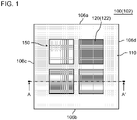
- Fig. 1 is a top view of a ceramic circuit board 100 according to Embodiment 1.
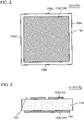
- Fig. 2 is a bottom view of the ceramic circuit board 100 shown in Fig. 1 .
- Fig. 3 is a cross-sectional view taken along the line A-A' of Fig. 1 .
- the ceramic circuit board 100 includes a marker portion 150.
- the marker portion 150 is formed on the surface of the ceramic circuit board 100. Information concerning the ceramic circuit board 100 can be acquired from the marker portion 150.
- the details of the ceramic circuit board 100 will be described by using Fig. 1 to Fig. 3 .
- the ceramic circuit board 100 includes a ceramic base material 110, a metal layer 120 (a first metal layer 122 and a second metal layer 124), and a marker portion 150.
- the ceramic circuit board 100 (ceramic base material 110) has a first surface 102, a second surface 104, and side faces (in the example shown in Fig. 1 , a first side surface 106a, a second side surface 106b, a third side surface 106c, and a fourth side surface 106d) .
- the second surface 104 is opposite to the first surface 102.
- Each side face is between the first surface 102 and the second surface 104.
- the second side surface 106b is opposite to the first side surface 106a.
- the third side surface 106c is between the first side surface 106a and the second side surface 106b.
- the fourth side surface 106d is opposite to the third side surface 106c.
- the first surface 102 and the second surface 104 of the ceramic base material 110 have a substantially rectangular shape.
- This rectangle may not be an exact rectangle, and the rectangle may have, for example, sides with sections formed therein or may have rounded corners.
- the first surface 102 and the second surface 104 of the ceramic base material 110 may have a shape other than a rectangle.
- the ceramic base material 110 is formed from, for example, AlN, Si 3 N 4 , or Al 2 O 3 .
- the thickness of the ceramic base material 110 is, for example, equal to or more than 0.2 mm and equal to or less than 1.5 mm.
- the first metal layer 122 is located on the first surface 102 of the ceramic base material 110.
- the second metal layer 124 is located on the second surface 104 of the ceramic base material 110.
- the first metal layer 122 forms a metal pattern (for example, a circuit pattern) . In the example shown in Fig. 1 , this metal pattern includes four rectangular patterns arranged adjacently. However, the metal pattern is not limited to this example.
- the second metal layer 124 extends over almost the entire second surface 104 of the ceramic base material 110. However, the area of the second metal layer 124 is slightly smaller than the area of the second surface 104.
- the area of the second metal layer 124 is, for example, equal to or more than 80% and equal to or less than 97% of the area of the second surface 104.
- the ratio of the area of the first metal layer 122 with respect to the area of the first surface 102 is smaller than the ratio of the area of the second metal layer 124 with respect to the area of the second surface 104.
- the metal layer 120 is formed from at least one selected from the group consisting of, for example, Cu, Al, Mo, an alloy including Cu and Mo, and an alloy including Cu and W.
- the thickness of the metal layer 120 is, for example, equal to or more than 0.1 mm and equal to or less than 2 mm.
- the surface of the metal layer 120 may be plated.
- the plating applied to the surface of the metal layer 120 is formed from at least one selected from the group consisting of, for example, Ni, Au, Ag, and Cu.
- the marker portion 150 is formed on the surface of the first metal layer 122. However, the marker portion 150 may be formed on the surface of the second metal layer 124 or may be formed on both the surface of the first metal layer 122 and the surface of the second metal layer 124. When the surface of the metal layer 120 (first metal layer 122 or second metal layer 124) is plated, the marker portion 150 may be formed on the surface of the plating or may be covered by the plating.
- the marker portion 150 indicates information concerning the ceramic circuit board 100.
- the information concerning the ceramic circuit board 100 is, for example, information including the production conditions for the ceramic circuit board 100.
- the information including the production conditions for the ceramic circuit board 100 includes, for example, the quality or quantity of the material used for the production of the ceramic circuit board 100, the time or temperature for heating of the ceramic circuit board 100, and the like.
- the traceability of the ceramic circuit board 100 can be enhanced by acquiring information including the production conditions for the ceramic circuit board 100 from the marker portion 150.
- the shape of the marker portion 150 is not limited to a specific shape.
- the marker portion 150 is illustratively a one-dimensional code (bar code).
- the marker portion 150 may be a two-dimensional code.
- the marker portion 150 may be both a one-dimensional code and a two-dimensional code.
- the marker portion 150 can include so much information concerning the ceramic circuit board 100.
- the marker portion 150 may include, for example, at least one selected from the group consisting of letters, numbers, and symbols.
- the marker portion 150 can include various structures formed on the surface of the ceramic base material 110.
- the marker portion 150 is a recess portion formed on the surface of a metal layer 120 (first metal layer 122) of a ceramic base material 110.
- the recess portion is formed, for example, by a laser on the surface of the metal layer 120 (first metal layer 122) of the ceramic base material 110.
- the recess portion may be formed by a method other than a laser, such as etching. By using a laser, equipment can be easily added into the line of continuous processes, and thus the marker portion 150 can be easily added without impairing productivity by adding a new process.
- the recess portion is a recess portion formed by a laser
- the marker portion (recess portion) can be formed in a region as small as equal to or more than 1 mm 2 and equal to or less than 100 mm 2
- the marker portion (recess portion) can be easily provided even in a narrow region that does not affect the performance of the product.
- Examples of the narrow region that does not affect the performance of the product may include sites that are not used for assembling, such as soldering and wire bonding.
- a code such as a two-dimensional code with a laser
- a large amount of information can be recorded even in a small marker portion.
- a laser for example, a recess portion having a width of equal to or more than 10 um and equal to or less than 200 um and a depth of equal to or more than 10 um and equal to or less than 200 um can be formed, and thus a code can be formed in a small region.
- These recess portions formed by lasers are useful also in other embodiments.
- the marker portion 150 may be formed by a coating material.
- the coating material is, for example, a solder resist and is applied by, for example, inkjetting.
- Fig. 4 is a top view of a heat-dissipating member 200 according to Embodiment 2.
- Fig. 5 is a cross-sectional view taken along the line B-B' of Fig. 4 .
- the heat-dissipating member 200 includes a first surface 202 and a second surface 204.
- the second surface 204 is opposite to the first surface 202.
- a heat-dissipating fin 210 is attached to the first surface 202 via grease 212.
- the heat-dissipating fin 210 is attached to the first surface 202 via the grease 212, after an electronic element (not shown in the drawings) such as a Si semiconductor element is mounted on the second surface 204 via a ceramic circuit board (for example, the ceramic circuit board 100 of Embodiment 1) (not shown in the drawings), to form a power module by the heat-dissipating member 200, the ceramic circuit board, and the electronic element.
- the heat-dissipating fin 210 may be screwed to the first surface 202 of the heat-dissipating member 200.
- a marker portion 250 is formed on the second surface 204. Information concerning the heat-dissipating member 200 can be acquired from the marker portion 250.
- the marker portion 250 is formed on the surface opposite to the heat-dissipating fin 210 (second surface 204), the marker portion 250 does not interfere with the heat conduction from the heat-dissipating member 200 to the heat-dissipating fin 210.
- the heat-dissipating member 200 has a first surface 202, a second surface 204, and side faces (in the example shown in Fig. 4 , a first side surface 206a, a second side surface 206b, a third side surface 206c, and a fourth side surface 206d). Each side face is between the first surface 202 and the second surface 204.
- the second side surface 206b is opposite to the first side surface 206a.
- the third side surface 206c is between the first side surface 206a and the second side surface 206b.
- the fourth side surface 206d is opposite to the third side surface 206c.
- the second surface 204 of the heat-dissipating member 200 has a substantially rectangular shape. This rectangle may not be an exact rectangle, and the rectangle may have, for example, sides with sections formed therein or may have rounded corners.
- the second surface 204 of the heat-dissipating member 200 may have a shape other than a rectangle.
- the heat-dissipating member 200 is composed of, for example, a metal base composite composed of a metal containing Al or Mg as a main component (for example, equal to or more than 85% by mass) and at least one selected from the group consisting of SiC, Si 3 N 4 , Al 2 O 3 , SiO 2 , and AlN; an alloy including Cu and Mo or an alloy including Cu and W (for example, Cu/Mo or Cu/W alloy); or a multilayer metal plate formed from Cu and Mo or Cu and W (Cu/Mo or Cu/W multilayer metal plate).
- a metal base composite composed of a metal containing Al or Mg as a main component (for example, equal to or more than 85% by mass) and at least one selected from the group consisting of SiC, Si 3 N 4 , Al 2 O 3 , SiO 2 , and AlN; an alloy including Cu and Mo or an alloy including Cu and W (for example, Cu/Mo or Cu/W alloy); or a multilayer metal plate formed from Cu
- the coefficient of linear expansion of the heat-dissipating member 200 is, for example, equal to or more than 5 ⁇ 10 -6 /K and equal to or less than 9 ⁇ 10 -6 /K.
- the thermal conductivity of the heat-dissipating member 200 is, for example, equal to or more than 150 W/mK.
- the surface of the heat-dissipating member 200 (for example, a first surface 202, a second surface 204, a first side surface 206a, a second side surface 206b, a third side surface 206c, and a fourth side surface 206d) is plated.
- the plating applied to the surface of the heat-dissipating member 200 is formed from at least one selected from the group consisting of, for example, Ni, Au, Ag, and Cu.
- the marker portion 250 may be formed on the surface of the plating or may be covered with the plating.
- the marker portion 250 indicates information concerning the heat-dissipating member 200.
- the information concerning the heat-dissipating member 200 is, for example, information including the direction of warpage of the heat-dissipating member 200.
- the marker portion 250 is located on the second surface 204 side.
- the heat-dissipating member 200 is warped convexly from the first surface 202 toward the second surface 204, and the heat-dissipating fin 210 is attached to the first surface 202, the heat-dissipating fin 210 is not in with the heat-dissipating member 200 well, and satisfactory heat dissipation by the heat-dissipating fin 210 is not realized.
- the heat-dissipating member 200 is warped convexly from the second surface 204 toward the first surface 202, and the heat-dissipating fin 210 is attached to the first surface 202, the heat-dissipating fin 210 is in contact with the heat-dissipating member 200 well, and satisfactory heat dissipation by the heat-dissipating fin 210 is realized.
- the manufacturer of the electronic component can determine that it is preferable to attach the heat-dissipating fin 210 to the surface opposite to the marker portion 250 (that is, the first surface 202).
- the information concerning the heat-dissipating member 200 is, for example, information including the production conditions for the heat-dissipating member 200.
- the information including the production conditions for the heat-dissipating member 200 includes, for example, the quality or quantity of the material used for the production of the heat-dissipating member 200, the time or temperature for heating of the heat-dissipating member 200, and the like.
- the traceability of the heat-dissipating member 200 can be enhanced by acquiring the information including the production conditions for the heat-dissipating member 200 from the marker portion 250.
- the shape of the marker portion 250 is not limited to a specific shape.
- the marker portion 250 is illustratively a one-dimensional code (bar code).
- the marker portion 250 may be a two-dimensional code.
- the marker portion 250 may be both a one-dimensional code and a two-dimensional code.
- the marker portion 250 can include so much information concerning the heat-dissipating member 200.
- the marker portion 250 may include, for example, at least one selected from the group consisting of letters, numbers, and symbols.
- the marker portion 250 can include various structures formed on the surface of the heat-dissipating member 200.
- the marker portion 250 is a recess portion formed on the surface (second surface 204) of the heat-dissipating member 200.
- the recess portion is formed by, for example, a laser on the surface (second surface 204) of the heat-dissipating member 200.
- the recess portion may be formed by a method other than a laser, such as etching.
- the marker portion 250 may be formed by a coating material.
- the coating material may be, for example, the same as the coating material used for the marker portion 150 of Embodiment 1.
- Fig. 6 is a top view of an aluminum-diamond composite 300 according to Embodiment 3.
- Fig. 7 is a cross-sectional view taken along the line C-C' of Fig. 6 .
- the aluminum-diamond composite 300 is a flat plate including diamond particles and a metal containing aluminum as a main component.
- the aluminum-diamond composite 300 is composed of a composited portion 310 and surface layers 320 (first surface layer 322 and second surface layer 324) provided on both faces of the composited portion 310.
- the surface layer 320 is composed of a material including a metal containing aluminum as a main component.
- the aluminum-diamond composite 300 includes a marker portion 350.
- the marker portion 350 is formed on the surface of the surface layer 320. Information concerning the aluminum-diamond composite 300 can be acquired from the marker portion 350.
- the aluminum-diamond composite 300 has a first surface 302, a second surface 304, and side faces (in the example shown in Fig. 6 , a first side surface 306a, a second side surface 306b, a third side surface 306c, and a fourth side surface 306d).
- the second surface 304 is opposite to the first surface 302. Each side face is between the first surface 302 and the second surface 304.
- the second side surface 306b is opposite to the first side surface 306a.
- the third side surface 306c is between the first side surface 306a and the second side surface 306b.
- the fourth side surface 306d is opposite to the third side surface 306c.
- the first surface 302 of the aluminum-diamond composite 300 has a substantially rectangular shape. This rectangle may not be an exact rectangle, and the rectangle may have, for example, sides with sections formed therein or may have rounded corners.
- the first surface 302 of the aluminum-diamond composite 300 may have a shape other than a rectangle.
- the thickness of the aluminum-diamond composite 300 is, for example, equal to or more than 0.4 mm and equal to or less than 6 mm.
- the composited portion 310 is a composited portion of diamond particles and an aluminum alloy.
- the content of the diamond particles is, for example, equal to or more than 40% by volume and equal to or less than 75% by volume with respect to the total volume of the aluminum-diamond composite 300.
- the aluminum alloy is a metal containing aluminum as a main component.
- the aluminum alloy includes, for example, equal to or more than 75% by mass of aluminum with respect to the total mass of the aluminum alloy.
- the aluminum alloy may include equal to or more than 5% by mass and equal to or less than 25% by mass of silicon with respect to the total mass of the aluminum alloy.
- the aluminum alloy may further include magnesium.
- the surface layer 320 is composed of a material including a metal containing aluminum as a main component.
- the surface layer 320 includes, for example, equal to or more than 80% by volume of the metal with respect to the total volume of the surface layer 320.
- the surface roughness Ra of the surface layer 320 is, for example, equal to or less than 1 um.
- a Ni plating layer or two layers of Ni plating and Au plating may be formed with a thickness of, for example, equal to or more than 0.5 um and equal to or less than 10 ⁇ m.
- the marker portion 350 indicates information concerning the aluminum-diamond composite 300.
- the information concerning the aluminum-diamond composite 300 is, for example, information including the production conditions for the aluminum-diamond composite 300.
- the information including the production conditions for the aluminum-diamond composite 300 includes, for example, the quality or quantity of the material used in the production of the aluminum-diamond composite 300, the time or temperature for heating of the aluminum-diamond composite 300, and the like.
- the traceability of the aluminum-diamond composite 300 can be enhanced by acquiring the information including the production conditions for the aluminum-diamond composite 300 from the marker portion 350.
- the shape of the marker portion 350 is not limited to a specific shape.
- the marker portion 350 is illustratively a one-dimensional code (bar code).
- the marker portion 350 may be a two-dimensional code.
- the marker portion 350 may be both a one-dimensional code and a two-dimensional code.
- the marker portion 350 can include so much information concerning the aluminum-diamond composite 300.
- the marker portion 350 may include, for example, at least one selected from the group consisting of letters, numbers, and symbols.
- the marker portion 350 can include various structures formed on the surface of the aluminum-diamond composite 300.
- the marker portion 350 is a recess portion formed on the surface of the aluminum-diamond composite 300.
- the recess portion is formed on, for example, the aluminum-diamond composite 300 by a laser.
- the recess portion may be formed by a method other than a laser, such as etching.
- the marker portion 350 may be formed by a coating material.
- the coating material may be, for example, the same as the coating material used for the marker portion 150 of Embodiment 1.
Landscapes
- Engineering & Computer Science (AREA)
- Physics & Mathematics (AREA)
- Microelectronics & Electronic Packaging (AREA)
- General Physics & Mathematics (AREA)
- Theoretical Computer Science (AREA)
- Thermal Sciences (AREA)
- Structure Of Printed Boards (AREA)
- Cooling Or The Like Of Semiconductors Or Solid State Devices (AREA)
- Geometry (AREA)
- Cooling Or The Like Of Electrical Apparatus (AREA)
Abstract
Description
- The present invention relates to a ceramic circuit board, a heat-dissipating member, and an aluminum-diamond composite.
- In recent years, ceramic circuit boards and heat-dissipating members have been used as electronic components. The ceramic circuit board is mounted on a heat-dissipating member. Various electronic elements such as Si semiconductor elements are mounted on the ceramic circuit board.
- Patent Document 1 describes that a marker pattern is formed on a ceramic circuit board. The marker pattern is formed by, for example, a laser. The marker pattern is arranged in the form of, for example, a bar code or a matrix code. The marker pattern indicates, for example, the model, type characteristics, performance, or size of a ceramic circuit board.
- Patent Document 2 describes that an aluminum-diamond composite is used as a heat-dissipating member such as a heat sink. The aluminum-diamond composite includes diamond particles and a metal containing aluminum as a main component. The aluminum-diamond composite includes a composited portion and a surface layer provided on both faces of the composited portion. The surface layer is composed of a metal containing aluminum as a main component.
-
- [Patent Document 1]
European Unexamined Patent Publication No. 3361504 - [Patent Document 2] Pamphlet of International Publication No.
WO 2010/007922 - In various situations such as a production process for an electronic component, it may be required to acquire information concerning members used for the electronic component (for example, a ceramic circuit board, a heat-dissipating member, or an aluminum-diamond composite).
- An example of an object of the present invention is to acquire information concerning a member used for an electronic component by a novel method. Other objects of the present invention will become apparent from the description of the present specification.
- An aspect of the present invention is a ceramic circuit board including:
- a metal layer; and
- a marker portion formed on a surface of the metal layer.
- Another aspect of the present invention is a heat-dissipating member, the heat-dissipating member including:
- a first surface on which a heat-dissipating fin is attached; and
- a second surface opposite to the first surface, in which a marker portion is formed on the second surface.
- Still another aspect of the invention is an aluminum-diamond composite having a flat plate shape and including diamond particles and a metal containing aluminum as a main component,
- in which the aluminum-diamond composite includes a composited portion and surface layers provided on both faces of the composited portion,
- the surface layer is composed of a material including a metal containing aluminum as a main component, and
- the aluminum-diamond composite includes a marker portion formed on a surface of the surface layer.
- According to an aspect of the present invention, information concerning a member used for an electronic component can be obtained by a novel method.
-
-
Fig. 1 is a top view of a ceramic circuit board according to Embodiment 1. -
Fig. 2 is a bottom view of the ceramic circuit board shown inFig. 1 . -
Fig. 3 is a cross-sectional view taken along the line A-A' inFig. 1 . -
Fig. 4 is a top view of a heat-dissipating member according to Embodiment 2. -
Fig. 5 is a cross-sectional view taken along the line B-B' inFig. 4 . -
Fig. 6 is a top view of an aluminum-diamond composite according to Embodiment 3. -
Fig. 7 is a cross-sectional view taken along the line C-C' inFig. 6 . - Hereinafter, embodiments of the present invention will be described using the drawings. In all the drawings, similar constituent elements will be assigned with similar reference numerals, and further description thereof will not be repeated as appropriate.
-
Fig. 1 is a top view of aceramic circuit board 100 according to Embodiment 1.Fig. 2 is a bottom view of theceramic circuit board 100 shown inFig. 1 .Fig. 3 is a cross-sectional view taken along the line A-A' ofFig. 1 . - An outline of the
ceramic circuit board 100 will be described by usingFig. 1 to Fig. 3 . Theceramic circuit board 100 includes amarker portion 150. Themarker portion 150 is formed on the surface of theceramic circuit board 100. Information concerning theceramic circuit board 100 can be acquired from themarker portion 150. - The details of the
ceramic circuit board 100 will be described by usingFig. 1 to Fig. 3 . - The
ceramic circuit board 100 includes aceramic base material 110, a metal layer 120 (afirst metal layer 122 and a second metal layer 124), and amarker portion 150. - The ceramic circuit board 100 (ceramic base material 110) has a
first surface 102, asecond surface 104, and side faces (in the example shown inFig. 1 , afirst side surface 106a, asecond side surface 106b, athird side surface 106c, and afourth side surface 106d) . Thesecond surface 104 is opposite to thefirst surface 102. Each side face is between thefirst surface 102 and thesecond surface 104. Thesecond side surface 106b is opposite to thefirst side surface 106a. Thethird side surface 106c is between thefirst side surface 106a and thesecond side surface 106b. Thefourth side surface 106d is opposite to thethird side surface 106c. In the examples shown inFig. 1 andFig. 2 , thefirst surface 102 and thesecond surface 104 of theceramic base material 110 have a substantially rectangular shape. This rectangle may not be an exact rectangle, and the rectangle may have, for example, sides with sections formed therein or may have rounded corners. Thefirst surface 102 and thesecond surface 104 of theceramic base material 110 may have a shape other than a rectangle. - The
ceramic base material 110 is formed from, for example, AlN, Si3N4, or Al2O3. The thickness of theceramic base material 110 is, for example, equal to or more than 0.2 mm and equal to or less than 1.5 mm. - The
first metal layer 122 is located on thefirst surface 102 of theceramic base material 110. Thesecond metal layer 124 is located on thesecond surface 104 of theceramic base material 110. Thefirst metal layer 122 forms a metal pattern (for example, a circuit pattern) . In the example shown inFig. 1 , this metal pattern includes four rectangular patterns arranged adjacently. However, the metal pattern is not limited to this example. Thesecond metal layer 124, on the other hand, extends over almost the entiresecond surface 104 of theceramic base material 110. However, the area of thesecond metal layer 124 is slightly smaller than the area of thesecond surface 104. The area of thesecond metal layer 124 is, for example, equal to or more than 80% and equal to or less than 97% of the area of thesecond surface 104. The ratio of the area of thefirst metal layer 122 with respect to the area of thefirst surface 102 is smaller than the ratio of the area of thesecond metal layer 124 with respect to the area of thesecond surface 104. - The
metal layer 120 is formed from at least one selected from the group consisting of, for example, Cu, Al, Mo, an alloy including Cu and Mo, and an alloy including Cu and W. The thickness of themetal layer 120 is, for example, equal to or more than 0.1 mm and equal to or less than 2 mm. The surface of themetal layer 120 may be plated. The plating applied to the surface of themetal layer 120 is formed from at least one selected from the group consisting of, for example, Ni, Au, Ag, and Cu. - The
marker portion 150 is formed on the surface of thefirst metal layer 122. However, themarker portion 150 may be formed on the surface of thesecond metal layer 124 or may be formed on both the surface of thefirst metal layer 122 and the surface of thesecond metal layer 124. When the surface of the metal layer 120 (first metal layer 122 or second metal layer 124) is plated, themarker portion 150 may be formed on the surface of the plating or may be covered by the plating. - The
marker portion 150 indicates information concerning theceramic circuit board 100. - In one example, the information concerning the
ceramic circuit board 100 is, for example, information including the production conditions for theceramic circuit board 100. The information including the production conditions for theceramic circuit board 100 includes, for example, the quality or quantity of the material used for the production of theceramic circuit board 100, the time or temperature for heating of theceramic circuit board 100, and the like. In this example, the traceability of theceramic circuit board 100 can be enhanced by acquiring information including the production conditions for theceramic circuit board 100 from themarker portion 150. - The shape of the
marker portion 150 is not limited to a specific shape. In the example shown inFig. 1 , themarker portion 150 is illustratively a one-dimensional code (bar code). Themarker portion 150 may be a two-dimensional code. Themarker portion 150 may be both a one-dimensional code and a two-dimensional code. When themarker portion 150 is at least one of a one-dimensional code and a two-dimensional code, themarker portion 150 can include so much information concerning theceramic circuit board 100. As another example, themarker portion 150 may include, for example, at least one selected from the group consisting of letters, numbers, and symbols. - The
marker portion 150 can include various structures formed on the surface of theceramic base material 110. - In one example, the
marker portion 150 is a recess portion formed on the surface of a metal layer 120 (first metal layer 122) of aceramic base material 110. The recess portion is formed, for example, by a laser on the surface of the metal layer 120 (first metal layer 122) of theceramic base material 110. The recess portion may be formed by a method other than a laser, such as etching. By using a laser, equipment can be easily added into the line of continuous processes, and thus themarker portion 150 can be easily added without impairing productivity by adding a new process. When the recess portion is a recess portion formed by a laser, since the marker portion (recess portion) can be formed in a region as small as equal to or more than 1 mm2 and equal to or less than 100 mm2, the marker portion (recess portion) can be easily provided even in a narrow region that does not affect the performance of the product. Examples of the narrow region that does not affect the performance of the product may include sites that are not used for assembling, such as soldering and wire bonding. When the marker portion is a marker portion formed by a laser, there is almost no possibility that the marker portion will disappear during the production process, and information can be acquired even after the product is used for a long time period. Particularly, by forming a code such as a two-dimensional code with a laser, a large amount of information can be recorded even in a small marker portion. When a laser is used, for example, a recess portion having a width of equal to or more than 10 um and equal to or less than 200 um and a depth of equal to or more than 10 um and equal to or less than 200 um can be formed, and thus a code can be formed in a small region. These recess portions formed by lasers are useful also in other embodiments. - In another example, the
marker portion 150 may be formed by a coating material. The coating material is, for example, a solder resist and is applied by, for example, inkjetting. -
Fig. 4 is a top view of a heat-dissipatingmember 200 according to Embodiment 2.Fig. 5 is a cross-sectional view taken along the line B-B' ofFig. 4 . - An outline of the heat-dissipating
member 200 will be described by usingFig. 4 and Fig. 5 . The heat-dissipatingmember 200 includes afirst surface 202 and asecond surface 204. Thesecond surface 204 is opposite to thefirst surface 202. A heat-dissipatingfin 210 is attached to thefirst surface 202 viagrease 212. The heat-dissipatingfin 210 is attached to thefirst surface 202 via thegrease 212, after an electronic element (not shown in the drawings) such as a Si semiconductor element is mounted on thesecond surface 204 via a ceramic circuit board (for example, theceramic circuit board 100 of Embodiment 1) (not shown in the drawings), to form a power module by the heat-dissipatingmember 200, the ceramic circuit board, and the electronic element. In this case, the heat-dissipatingfin 210 may be screwed to thefirst surface 202 of the heat-dissipatingmember 200. Amarker portion 250 is formed on thesecond surface 204. Information concerning the heat-dissipatingmember 200 can be acquired from themarker portion 250. In addition, since themarker portion 250 is formed on the surface opposite to the heat-dissipating fin 210 (second surface 204), themarker portion 250 does not interfere with the heat conduction from the heat-dissipatingmember 200 to the heat-dissipatingfin 210. - The details of the heat-dissipating
member 200 will be described by usingFig. 4 and Fig. 5 . - The heat-dissipating
member 200 has afirst surface 202, asecond surface 204, and side faces (in the example shown inFig. 4 , afirst side surface 206a, asecond side surface 206b, athird side surface 206c, and afourth side surface 206d). Each side face is between thefirst surface 202 and thesecond surface 204. Thesecond side surface 206b is opposite to thefirst side surface 206a. Thethird side surface 206c is between thefirst side surface 206a and thesecond side surface 206b. Thefourth side surface 206d is opposite to thethird side surface 206c. In the example shown inFig. 4 , thesecond surface 204 of the heat-dissipatingmember 200 has a substantially rectangular shape. This rectangle may not be an exact rectangle, and the rectangle may have, for example, sides with sections formed therein or may have rounded corners. Thesecond surface 204 of the heat-dissipatingmember 200 may have a shape other than a rectangle. - The heat-dissipating
member 200 is composed of, for example, a metal base composite composed of a metal containing Al or Mg as a main component (for example, equal to or more than 85% by mass) and at least one selected from the group consisting of SiC, Si3N4, Al2O3, SiO2, and AlN; an alloy including Cu and Mo or an alloy including Cu and W (for example, Cu/Mo or Cu/W alloy); or a multilayer metal plate formed from Cu and Mo or Cu and W (Cu/Mo or Cu/W multilayer metal plate). The coefficient of linear expansion of the heat-dissipatingmember 200 is, for example, equal to or more than 5×10⁻⁶/K and equal to or less than 9×10⁻⁶/K. The thermal conductivity of the heat-dissipatingmember 200 is, for example, equal to or more than 150 W/mK. - It is preferable that the surface of the heat-dissipating member 200 (for example, a
first surface 202, asecond surface 204, afirst side surface 206a, asecond side surface 206b, athird side surface 206c, and afourth side surface 206d) is plated. The plating applied to the surface of the heat-dissipatingmember 200 is formed from at least one selected from the group consisting of, for example, Ni, Au, Ag, and Cu. When the surface of the heat-dissipatingmember 200 is plated, themarker portion 250 may be formed on the surface of the plating or may be covered with the plating. - The
marker portion 250 indicates information concerning the heat-dissipatingmember 200. - In one example, the information concerning the heat-dissipating
member 200 is, for example, information including the direction of warpage of the heat-dissipatingmember 200. For example, when the heat-dissipatingmember 200 is warped convexly from thesecond surface 204 toward thefirst surface 202, it is preferable that themarker portion 250 is located on thesecond surface 204 side. If the heat-dissipatingmember 200 is warped convexly from thefirst surface 202 toward thesecond surface 204, and the heat-dissipatingfin 210 is attached to thefirst surface 202, the heat-dissipatingfin 210 is not in with the heat-dissipatingmember 200 well, and satisfactory heat dissipation by the heat-dissipatingfin 210 is not realized. When, on the other hand, the heat-dissipatingmember 200 is warped convexly from thesecond surface 204 toward thefirst surface 202, and the heat-dissipatingfin 210 is attached to thefirst surface 202, the heat-dissipatingfin 210 is in contact with the heat-dissipatingmember 200 well, and satisfactory heat dissipation by the heat-dissipatingfin 210 is realized. When the heat-dissipatingmember 200 is warped convexly from thesecond surface 204 toward thefirst surface 202, and themarker portion 250 is located on thesecond surface 204 side, the manufacturer of the electronic component can determine that it is preferable to attach the heat-dissipatingfin 210 to the surface opposite to the marker portion 250 (that is, the first surface 202). - In another example, the information concerning the heat-dissipating
member 200 is, for example, information including the production conditions for the heat-dissipatingmember 200. The information including the production conditions for the heat-dissipatingmember 200 includes, for example, the quality or quantity of the material used for the production of the heat-dissipatingmember 200, the time or temperature for heating of the heat-dissipatingmember 200, and the like. In this example, the traceability of the heat-dissipatingmember 200 can be enhanced by acquiring the information including the production conditions for the heat-dissipatingmember 200 from themarker portion 250. - The shape of the
marker portion 250 is not limited to a specific shape. In the example shown inFig. 4 , themarker portion 250 is illustratively a one-dimensional code (bar code). Themarker portion 250 may be a two-dimensional code. Themarker portion 250 may be both a one-dimensional code and a two-dimensional code. When themarker portion 250 is at least one of a one-dimensional code and a two-dimensional code, themarker portion 250 can include so much information concerning the heat-dissipatingmember 200. As another example, themarker portion 250 may include, for example, at least one selected from the group consisting of letters, numbers, and symbols. - The
marker portion 250 can include various structures formed on the surface of the heat-dissipatingmember 200. - In one example, the
marker portion 250 is a recess portion formed on the surface (second surface 204) of the heat-dissipatingmember 200. The recess portion is formed by, for example, a laser on the surface (second surface 204) of the heat-dissipatingmember 200. The recess portion may be formed by a method other than a laser, such as etching. - In another example, the
marker portion 250 may be formed by a coating material. The coating material may be, for example, the same as the coating material used for themarker portion 150 of Embodiment 1. -
Fig. 6 is a top view of an aluminum-diamond composite 300 according to Embodiment 3.Fig. 7 is a cross-sectional view taken along the line C-C' ofFig. 6 . - An outline of the aluminum-
diamond composite 300 will be described by usingFig. 6 and Fig. 7 . The aluminum-diamond composite 300 is a flat plate including diamond particles and a metal containing aluminum as a main component. The aluminum-diamond composite 300 is composed of a compositedportion 310 and surface layers 320 (first surface layer 322 and second surface layer 324) provided on both faces of the compositedportion 310. Thesurface layer 320 is composed of a material including a metal containing aluminum as a main component. The aluminum-diamond composite 300 includes amarker portion 350. Themarker portion 350 is formed on the surface of thesurface layer 320. Information concerning the aluminum-diamond composite 300 can be acquired from themarker portion 350. - The details of the aluminum-
diamond composite 300 will be described by usingFig. 6 and Fig. 7 . - The aluminum-
diamond composite 300 has afirst surface 302, asecond surface 304, and side faces (in the example shown inFig. 6 , afirst side surface 306a, asecond side surface 306b, athird side surface 306c, and afourth side surface 306d). Thesecond surface 304 is opposite to thefirst surface 302. Each side face is between thefirst surface 302 and thesecond surface 304. Thesecond side surface 306b is opposite to thefirst side surface 306a. Thethird side surface 306c is between thefirst side surface 306a and thesecond side surface 306b. Thefourth side surface 306d is opposite to thethird side surface 306c. In the example shown inFig. 6 , thefirst surface 302 of the aluminum-diamond composite 300 has a substantially rectangular shape. This rectangle may not be an exact rectangle, and the rectangle may have, for example, sides with sections formed therein or may have rounded corners. Thefirst surface 302 of the aluminum-diamond composite 300 may have a shape other than a rectangle. - The thickness of the aluminum-
diamond composite 300 is, for example, equal to or more than 0.4 mm and equal to or less than 6 mm. - The composited
portion 310 is a composited portion of diamond particles and an aluminum alloy. The content of the diamond particles is, for example, equal to or more than 40% by volume and equal to or less than 75% by volume with respect to the total volume of the aluminum-diamond composite 300. The aluminum alloy is a metal containing aluminum as a main component. The aluminum alloy includes, for example, equal to or more than 75% by mass of aluminum with respect to the total mass of the aluminum alloy. The aluminum alloy may include equal to or more than 5% by mass and equal to or less than 25% by mass of silicon with respect to the total mass of the aluminum alloy. The aluminum alloy may further include magnesium. - The
surface layer 320 is composed of a material including a metal containing aluminum as a main component. Thesurface layer 320 includes, for example, equal to or more than 80% by volume of the metal with respect to the total volume of thesurface layer 320. The surface roughness Ra of thesurface layer 320 is, for example, equal to or less than 1 um. On the surface of thesurface layer 320, a Ni plating layer or two layers of Ni plating and Au plating may be formed with a thickness of, for example, equal to or more than 0.5 um and equal to or less than 10 µm. - The
marker portion 350 indicates information concerning the aluminum-diamond composite 300. - In one example, the information concerning the aluminum-
diamond composite 300 is, for example, information including the production conditions for the aluminum-diamond composite 300. The information including the production conditions for the aluminum-diamond composite 300 includes, for example, the quality or quantity of the material used in the production of the aluminum-diamond composite 300, the time or temperature for heating of the aluminum-diamond composite 300, and the like. In this example, the traceability of the aluminum-diamond composite 300 can be enhanced by acquiring the information including the production conditions for the aluminum-diamond composite 300 from themarker portion 350. - The shape of the
marker portion 350 is not limited to a specific shape. In the example shown inFig. 6 , themarker portion 350 is illustratively a one-dimensional code (bar code). Themarker portion 350 may be a two-dimensional code. Themarker portion 350 may be both a one-dimensional code and a two-dimensional code. When themarker portion 350 is at least one of a one-dimensional code and a two-dimensional code, themarker portion 350 can include so much information concerning the aluminum-diamond composite 300. As another example, themarker portion 350 may include, for example, at least one selected from the group consisting of letters, numbers, and symbols. - The
marker portion 350 can include various structures formed on the surface of the aluminum-diamond composite 300. - In one example, the
marker portion 350 is a recess portion formed on the surface of the aluminum-diamond composite 300. The recess portion is formed on, for example, the aluminum-diamond composite 300 by a laser. The recess portion may be formed by a method other than a laser, such as etching. - In another example, the
marker portion 350 may be formed by a coating material. The coating material may be, for example, the same as the coating material used for themarker portion 150 of Embodiment 1. - Although embodiments of the present invention have been described with reference to the drawings, these are merely examples of the present invention, and various configurations other than the above-described ones may be adopted.
- This patent application claims priority based on
Japanese Patent Application No. 2020-055457, filed on March 26, 2020 -
- 100:
- ceramic circuit board
- 102:
- first surface
- 104:
- second surface
- 106a:
- first side surface
- 106b:
- second side surface
- 106c:
- third side surface
- 106d:
- fourth side surface
- 110:
- ceramic base material
- 120:
- metal layer
- 122:
- first metal layer
- 124:
- second metal layer
- 150:
- marker portion
- 200:
- marker
- 200:
- heat-dissipating member
- 202:
- recess portion
- 202:
- first surface
- 204:
- second surface
- 206a:
- first side surface
- 206b:
- second side surface
- 206c:
- third side surface
- 206d:
- fourth side surface
- 210:
- heat-dissipating fin
- 212:
- grease
- 250:
- marker portion
- 302:
- first surface
- 304:
- second surface
- 306a:
- first side surface
- 306b:
- second side surface
- 306c:
- third side surface
- 306d:
- fourth side surface
- 310:
- composited portion
- 320:
- surface layer
- 322:
- first surface layer
- 324:
- second surface layer
- 350:
- marker portion
Claims (16)
- A ceramic circuit board comprising:a metal layer; anda marker portion formed on a surface of the metal layer.
- The ceramic circuit board according to claim 1,
wherein the marker portion is a recess portion formed by a laser on the surface of the metal layer. - The ceramic circuit board according to claim 1,
wherein the marker portion is formed by a coating material. - The ceramic circuit board according to any one of claims 1 to 3,
wherein the marker portion is at least one of a one-dimensional code and a two-dimensional code. - The ceramic circuit board according to any one of claims 1 to 4,
wherein the marker portion indicates information including production conditions for the ceramic circuit board. - A heat-dissipating member, comprising:a first surface on which a heat-dissipating fin is attached; anda second surface opposite to the first surface, wherein a marker portion is formed on the second surface.
- The heat-dissipating member according to claim 6,
wherein the marker portion is a recess portion formed by a laser on the second surface of the heat-dissipating member. - The heat-dissipating member according to claim 6,
wherein the marker portion is formed by a coating material. - The heat-dissipating member according to any one of claims 6 to 8,
wherein the marker portion is at least one of a one-dimensional code and a two-dimensional code. - The heat-dissipating member according to any one of claims 6 to 9,
wherein the marker portion indicates information including a direction of warpage of the heat-dissipating member. - The heat-dissipating member according to any one of claims 6 to 10,
wherein the marker portion indicates information including production conditions for the heat-dissipating member. - An aluminum-diamond composite having a flat plate shape, comprising diamond particles and a metal containing aluminum as a main component,wherein the aluminum-diamond composite includes a composited portion and surface layers provided on both faces of the composited portion,the surface layer is composed of a material including a metal containing aluminum as a main component, andthe aluminum-diamond composite includes a marker portion formed on a surface of the surface layer.
- The aluminum-diamond composite according to claim 12,
wherein the marker portion is a recess portion formed by a laser on the surface. - The aluminum-diamond composite according to claim 12,
wherein the marker portion is formed by a coating material. - The aluminum-diamond composite according to any one of claims 12 to 14,
wherein the marker portion is at least one of a one-dimensional code and a two-dimensional code. - The aluminum-diamond composite according to any one of claims 12 to 15,
wherein the marker portion indicates information including production conditions for the aluminum-diamond composite.
Applications Claiming Priority (2)
| Application Number | Priority Date | Filing Date | Title |
|---|---|---|---|
| JP2020055457 | 2020-03-26 | ||
| PCT/JP2021/012500 WO2021193810A1 (en) | 2020-03-26 | 2021-03-25 | Ceramic circuit board, heat-dissipating member, and aluminum-diamond complex |
Publications (2)
| Publication Number | Publication Date |
|---|---|
| EP4131361A1 true EP4131361A1 (en) | 2023-02-08 |
| EP4131361A4 EP4131361A4 (en) | 2024-02-14 |
Family
ID=77891886
Family Applications (1)
| Application Number | Title | Priority Date | Filing Date |
|---|---|---|---|
| EP21776350.7A Ceased EP4131361A4 (en) | 2020-03-26 | 2021-03-25 | CERAMIC CIRCUIT BOARD, HEAT DISSIPATION ELEMENT AND ALUMINUM DIAMOND COMPLEX |
Country Status (6)
| Country | Link |
|---|---|
| US (1) | US11983586B2 (en) |
| EP (1) | EP4131361A4 (en) |
| JP (1) | JP7587570B2 (en) |
| KR (1) | KR20220159950A (en) |
| CN (1) | CN115053638A (en) |
| WO (1) | WO2021193810A1 (en) |
Cited By (1)
| Publication number | Priority date | Publication date | Assignee | Title |
|---|---|---|---|---|
| WO2025021816A1 (en) * | 2023-07-25 | 2025-01-30 | Rogers Germany Gmbh | Method for producing and/or handling a metal-ceramic substrate, a metal-ceramic substrate, a system for producing metal-ceramic substrates and database for metal-ceramic substrates |
Families Citing this family (1)
| Publication number | Priority date | Publication date | Assignee | Title |
|---|---|---|---|---|
| WO2022109552A1 (en) * | 2020-11-18 | 2022-05-27 | Sharfi Benjamin K | Diamond-based thermal cooling devices methods and materials |
Family Cites Families (24)
| Publication number | Priority date | Publication date | Assignee | Title |
|---|---|---|---|---|
| JPS62158034A (en) * | 1986-01-07 | 1987-07-14 | 川崎製鉄株式会社 | Metallic-foil composite body |
| JPH06333073A (en) * | 1993-05-18 | 1994-12-02 | Nichion Irika Kikai Seisakusho:Kk | Code mark reader |
| JP3361504B2 (en) | 2000-05-24 | 2003-01-07 | 株式会社イメ−ジパ−トナ− | Card payment automatic payment system |
| JP2002346633A (en) * | 2001-05-29 | 2002-12-03 | Daido Steel Co Ltd | Laser marking method |
| WO2003078353A1 (en) * | 2002-03-13 | 2003-09-25 | Schulz-Harder Juergen | Method for the production of a metal-ceramic substrate, preferably a copper-ceramic substrate |
| DE602005020839D1 (en) | 2004-11-01 | 2010-06-02 | Panasonic Corp | Light emitting module, lighting device and display device |
| JP2006253183A (en) * | 2005-03-08 | 2006-09-21 | Hitachi Ltd | Semiconductor power module |
| JP2009130156A (en) * | 2007-11-26 | 2009-06-11 | Seiko Epson Corp | Ceramic multilayer substrate and method for producing ceramic multilayer substrate |
| JP5940244B2 (en) * | 2008-07-17 | 2016-06-29 | デンカ株式会社 | Aluminum-diamond composite and method for producing the same |
| WO2012176473A1 (en) * | 2011-06-22 | 2012-12-27 | パナソニック株式会社 | Semiconductor substrate having dot markings, and method for producing same |
| JP5523415B2 (en) * | 2011-09-06 | 2014-06-18 | 三菱電機株式会社 | Cooling equipment, electrostatic atomizer and air conditioner |
| JP2013247256A (en) * | 2012-05-28 | 2013-12-09 | Hitachi Ltd | Semiconductor device and method of manufacturing the same |
| JP6091035B2 (en) * | 2014-10-29 | 2017-03-15 | 新電元工業株式会社 | Heat dissipation structure |
| US9799584B2 (en) * | 2015-11-16 | 2017-10-24 | Intel Corporation | Heat spreaders with integrated preforms |
| HUE064697T2 (en) * | 2015-12-22 | 2024-04-28 | Heraeus Electronics Gmbh & Co Kg | Method for the individual encoding of metal-ceramic substrates |
| WO2018123380A1 (en) * | 2016-12-28 | 2018-07-05 | デンカ株式会社 | Heat dissipation component for semiconductor element |
| CN109564908B (en) * | 2017-02-13 | 2022-06-24 | 富士电机株式会社 | Semiconductor device and method for manufacturing semiconductor device |
| EP3361504A1 (en) * | 2017-02-14 | 2018-08-15 | Infineon Technologies AG | Power electronic substrate with marker, manufacturing of a power electronic substrate and detection of a marker |
| JP6799479B2 (en) * | 2017-03-03 | 2020-12-16 | Dowaメタルテック株式会社 | Manufacturing method of metal-ceramic circuit board |
| DE112017008209B4 (en) * | 2017-11-17 | 2023-10-26 | Mitsubishi Electric Corporation | Semiconductor module |
| US10919326B2 (en) * | 2018-07-03 | 2021-02-16 | Apple Inc. | Controlled ablation and surface modification for marking an electronic device |
| FR3084667B1 (en) * | 2018-08-01 | 2020-12-25 | Saint Gobain Ct Recherches | PROCESS FOR MARKING A REFRACTORY CERAMIC PART |
| JP7129304B2 (en) | 2018-10-03 | 2022-09-01 | Toyo Tire株式会社 | tire |
| CN110690176B (en) * | 2019-10-14 | 2022-01-11 | 长江存储科技有限责任公司 | Method for distinguishing target crystal grains and failure analysis method of packaged chip |
-
2021
- 2021-03-25 KR KR1020227023670A patent/KR20220159950A/en not_active Ceased
- 2021-03-25 WO PCT/JP2021/012500 patent/WO2021193810A1/en not_active Ceased
- 2021-03-25 JP JP2022510653A patent/JP7587570B2/en active Active
- 2021-03-25 EP EP21776350.7A patent/EP4131361A4/en not_active Ceased
- 2021-03-25 CN CN202180010953.4A patent/CN115053638A/en active Pending
- 2021-03-25 US US17/791,971 patent/US11983586B2/en active Active
Cited By (1)
| Publication number | Priority date | Publication date | Assignee | Title |
|---|---|---|---|---|
| WO2025021816A1 (en) * | 2023-07-25 | 2025-01-30 | Rogers Germany Gmbh | Method for producing and/or handling a metal-ceramic substrate, a metal-ceramic substrate, a system for producing metal-ceramic substrates and database for metal-ceramic substrates |
Also Published As
| Publication number | Publication date |
|---|---|
| JPWO2021193810A1 (en) | 2021-09-30 |
| WO2021193810A1 (en) | 2021-09-30 |
| EP4131361A4 (en) | 2024-02-14 |
| KR20220159950A (en) | 2022-12-05 |
| US20230042932A1 (en) | 2023-02-09 |
| JP7587570B2 (en) | 2024-11-20 |
| CN115053638A (en) | 2022-09-13 |
| US11983586B2 (en) | 2024-05-14 |
Similar Documents
| Publication | Publication Date | Title |
|---|---|---|
| US7038313B2 (en) | Semiconductor device and method of manufacturing the same | |
| US7159310B2 (en) | Electronic part mounting substrate and method for producing same | |
| US6154364A (en) | Circuit board assembly with IC device mounted thereto | |
| US11983586B2 (en) | Ceramic circuit board, heat-dissipating member, and aluminum-diamond composite | |
| JP5619437B2 (en) | Method for producing metal / ceramic bonding substrate | |
| JP2008218938A (en) | Metal-ceramics bonded substrate | |
| JP2005011922A (en) | Double-sided copper-clad substrate with heat sink and semiconductor device using the same | |
| JPH11186331A (en) | Semiconductor device and its manufacture | |
| JP4806803B2 (en) | Metal-ceramic bonding substrate and manufacturing method thereof | |
| US20030224554A1 (en) | Package with a substrate of high thermal conductivity | |
| EP1518847B1 (en) | Aluminum/ceramic bonding substrate and method for producing same | |
| JPH08250823A (en) | Ceramics circuit board | |
| JP6799392B2 (en) | Metal-ceramic bonded substrate and its manufacturing method | |
| JPH09298259A (en) | Heat sink and method of manufacturing the same | |
| JP2006269966A (en) | Wiring board and manufacturing method thereof | |
| JP5631446B2 (en) | Method for producing metal / ceramic bonding substrate | |
| JPH10242330A (en) | Power module substrate and method of manufacturing the same | |
| JP2001298136A (en) | Heat sink and wiring board with the heat sink | |
| KR102257877B1 (en) | Heat sink plate | |
| KR102678847B1 (en) | Semiconductor package having coating layer for thermal emission and warpage prevention | |
| KR102908771B1 (en) | Ceramic substrate unit and manufacturing method thereof | |
| JP7796512B2 (en) | Metal-ceramic bonded substrate and manufacturing method thereof | |
| JP7267030B2 (en) | METAL-CERAMIC BONDING SUBSTRATE AND MANUFACTURING METHOD THEREOF | |
| JP2022171255A (en) | Metal-ceramic bonded substrate and manufacturing method for the same | |
| JPH04225296A (en) | Ceramic board provided with copper circuit and manufacture thereof |
Legal Events
| Date | Code | Title | Description |
|---|---|---|---|
| STAA | Information on the status of an ep patent application or granted ep patent |
Free format text: STATUS: THE INTERNATIONAL PUBLICATION HAS BEEN MADE |
|
| PUAI | Public reference made under article 153(3) epc to a published international application that has entered the european phase |
Free format text: ORIGINAL CODE: 0009012 |
|
| STAA | Information on the status of an ep patent application or granted ep patent |
Free format text: STATUS: REQUEST FOR EXAMINATION WAS MADE |
|
| 17P | Request for examination filed |
Effective date: 20221013 |
|
| AK | Designated contracting states |
Kind code of ref document: A1 Designated state(s): AL AT BE BG CH CY CZ DE DK EE ES FI FR GB GR HR HU IE IS IT LI LT LU LV MC MK MT NL NO PL PT RO RS SE SI SK SM TR |
|
| DAV | Request for validation of the european patent (deleted) | ||
| DAX | Request for extension of the european patent (deleted) | ||
| RIC1 | Information provided on ipc code assigned before grant |
Ipc: H05K 1/03 20060101ALN20230906BHEP Ipc: H01L 23/15 20060101ALN20230906BHEP Ipc: H01L 23/544 20060101ALI20230906BHEP Ipc: H01L 23/373 20060101ALI20230906BHEP Ipc: H05K 3/00 20060101ALI20230906BHEP Ipc: H05K 1/02 20060101ALI20230906BHEP Ipc: H01L 23/36 20060101ALI20230906BHEP Ipc: H01L 23/13 20060101AFI20230906BHEP |
|
| A4 | Supplementary search report drawn up and despatched |
Effective date: 20240115 |
|
| RIC1 | Information provided on ipc code assigned before grant |
Ipc: H05K 1/03 20060101ALN20240109BHEP Ipc: H01L 23/15 20060101ALN20240109BHEP Ipc: H01L 23/544 20060101ALI20240109BHEP Ipc: H01L 23/373 20060101ALI20240109BHEP Ipc: H05K 3/00 20060101ALI20240109BHEP Ipc: H05K 1/02 20060101ALI20240109BHEP Ipc: H01L 23/36 20060101ALI20240109BHEP Ipc: H01L 23/13 20060101AFI20240109BHEP |
|
| STAA | Information on the status of an ep patent application or granted ep patent |
Free format text: STATUS: EXAMINATION IS IN PROGRESS |
|
| 17Q | First examination report despatched |
Effective date: 20240806 |
|
| REG | Reference to a national code |
Ref country code: DE Ref legal event code: R003 |
|
| STAA | Information on the status of an ep patent application or granted ep patent |
Free format text: STATUS: THE APPLICATION HAS BEEN REFUSED |
|
| 18R | Application refused |
Effective date: 20250403 |