EP4131322B1 - Vorrichtung zur bestrahlung mit energiestrahlen - Google Patents
Vorrichtung zur bestrahlung mit energiestrahlen Download PDFInfo
- Publication number
- EP4131322B1 EP4131322B1 EP21787645.7A EP21787645A EP4131322B1 EP 4131322 B1 EP4131322 B1 EP 4131322B1 EP 21787645 A EP21787645 A EP 21787645A EP 4131322 B1 EP4131322 B1 EP 4131322B1
- Authority
- EP
- European Patent Office
- Prior art keywords
- unit
- filament
- emission device
- accommodation part
- filament unit
- Prior art date
- Legal status (The legal status is an assumption and is not a legal conclusion. Google has not performed a legal analysis and makes no representation as to the accuracy of the status listed.)
- Active
Links
Images

Classifications
-
- G—PHYSICS
- G21—NUCLEAR PHYSICS; NUCLEAR ENGINEERING
- G21K—TECHNIQUES FOR HANDLING PARTICLES OR IONISING RADIATION NOT OTHERWISE PROVIDED FOR; IRRADIATION DEVICES; GAMMA RAY OR X-RAY MICROSCOPES
- G21K5/00—Irradiation devices
-
- H—ELECTRICITY
- H01—ELECTRIC ELEMENTS
- H01J—ELECTRIC DISCHARGE TUBES OR DISCHARGE LAMPS
- H01J33/00—Discharge tubes with provision for emergence of electrons or ions from the vessel; Lenard tubes
- H01J33/02—Details
-
- H—ELECTRICITY
- H01—ELECTRIC ELEMENTS
- H01J—ELECTRIC DISCHARGE TUBES OR DISCHARGE LAMPS
- H01J33/00—Discharge tubes with provision for emergence of electrons or ions from the vessel; Lenard tubes
- H01J33/02—Details
- H01J33/04—Windows
-
- A—HUMAN NECESSITIES
- A61—MEDICAL OR VETERINARY SCIENCE; HYGIENE
- A61L—METHODS OR APPARATUS FOR STERILISING MATERIALS OR OBJECTS IN GENERAL; DISINFECTION, STERILISATION OR DEODORISATION OF AIR; CHEMICAL ASPECTS OF BANDAGES, DRESSINGS, ABSORBENT PADS OR SURGICAL ARTICLES; MATERIALS FOR BANDAGES, DRESSINGS, ABSORBENT PADS OR SURGICAL ARTICLES
- A61L2/00—Methods or apparatus for disinfecting or sterilising materials or objects other than foodstuffs or contact lenses; Accessories therefor
- A61L2/02—Methods or apparatus for disinfecting or sterilising materials or objects other than foodstuffs or contact lenses; Accessories therefor using physical phenomena
- A61L2/08—Radiation
- A61L2/087—Particle radiation, e.g. electron-beam, alpha or beta radiation
-
- H—ELECTRICITY
- H01—ELECTRIC ELEMENTS
- H01J—ELECTRIC DISCHARGE TUBES OR DISCHARGE LAMPS
- H01J1/00—Details of electrodes, of magnetic control means, of screens, or of the mounting or spacing thereof, common to two or more basic types of discharge tubes or lamps
- H01J1/88—Mounting, supporting, spacing, or insulating of electrodes or of electrode assemblies
Definitions
- the present disclosure relates to an energy beam emission device.
- Patent Literature 1 describes an electron beam emission device including a long electron discharge part.
- an electron discharge part is attached to a long connecting plate, and the connecting plate is slidably placed on a long rail.
- the electron discharge part can be taken out together with the connecting plate by the connecting plate being slid along the rail.
- Patent Literature 1 Japanese Unexamined Patent Publication No. 2003-149398
- the above-mentioned electron beam emission device has a configuration in which a lower surface of the long connecting plate is brought into contact with an upper surface of the long rail when an electron discharge unit including the electron discharge part is disposed in a housing. Therefore, this electron beam emission device is easily affected by the accuracy of each of the rail and the connecting plate, the arrangement accuracy of each member, and the like, and the electron discharge unit may not be stably disposed in the electron beam emission device.
- an object of the present disclosure is to provide an energy beam emission device capable of stably disposing an electron discharge unit.
- an electron beam emission device as defined in claim 1.
- the plurality of positioning parts are provided between the outer surface of the electron discharge unit and the inner surface of the unit accommodation part, the positioning parts being slidably in contact with the outer surface of the electron discharge unit or the inner surface of the unit accommodation part. That is, the long electron discharge unit is disposed in the unit accommodation part by being supported at a plurality of positions where the positioning parts are provided. As a result, in the energy beam emission device, it is possible to stably dispose the electron discharge unit even if the electron discharge unit has a long shape.
- the energy beam emission device may further include: a power supply part configured to supply electric power to the electron discharge unit, wherein the electron discharge unit may be capable of being inserted into the unit accommodation part from one end of the unit accommodation part, and wherein the power supply part may be provided in the housing on the other end side of the unit accommodation part and may be in contact with the electron discharge unit to be electrically connected to the electron discharge unit in a state where the electron discharge unit is inserted into the unit accommodation part.
- the energy beam emission device it is possible to electrically connect the electron discharge unit and the power supply part to each other by performing work of disposing the electron discharge unit in the unit accommodation part (work of inserting the electron discharge unit into the unit accommodation part) without performing special work for connecting the electron discharge unit and the power supply part.
- One end of the housing may be provided with an introduction opening into which the electron discharge unit is capable of being introduced and which is opened and closed by a lid.
- the electron discharge unit in the energy beam emission device, can be attached to and detached from the unit accommodation part via the introduction opening of the housing.
- An outer surface of the positioning part may have a protruding curved surface shape.
- the positioning part can slide smoothly with respect to the outer surface of the electron discharge unit or the inner surface of the unit accommodation part. As a result, in the energy beam emission device, the electron discharge unit can be easily attached to and detached from the unit accommodation part.
- the positioning part may include a spherical body that is in contact with the outer surface of the electron discharge unit or the inner surface of the unit accommodation part and a holding part that rotatably holds the spherical body.
- the electron discharge unit can smoothly slide in the unit accommodation part by the spherical body of the positioning part being rotated.
- the electron discharge unit can be easily attached to and detached from the unit accommodation part.
- the plurality of positioning parts may be provided in an extending direction of the electron discharge part.
- the positioning part may be provided at each of both ends on one side and the other side in an extending direction of the electron discharge part.
- the positioning part may be provided on the outer surface of the electron discharge unit and may be provided at each of a plurality of positions in an extending direction of the electron discharge part in a position on a tip end side in an insertion direction into the unit accommodation part with respect to a central position in the extending direction of the electron discharge part.
- two or more positioning parts disposed closer to the end on the tip end side in the insertion direction with respect to the central position in the extending direction come into contact with the unit accommodation part at an early stage of insertion.
- the electron discharge unit when the long electron discharge unit is inserted, the electron discharge unit is positioned with respect to the unit accommodation part at a stage at which the tip end thereof is inserted. As a result, in the energy beam emission device, it is possible to stably attach and detach the electron discharge unit to and from the unit accommodation part even in a case where the electron discharge unit has a long shape.
- the plurality of positioning parts may be provided in a circumferential direction of the electron discharge unit. In this case, in the energy beam emission device, it is possible to stabilize the position of the electron discharge unit in the unit accommodation part in a direction orthogonal to the extending direction of the electron discharge part.
- the energy beam emission device may further include: a projection projecting from an outer surface side of the unit accommodation part toward an inner surface side of the unit accommodation part, wherein the electron discharge unit may further have a rotation restricting member in which a groove extending in an extending direction of the electron discharge part is formed in an outer edge, and wherein a position of the electron discharge unit in a rotation direction in the unit accommodation part may be determined by the projection being fitted into the groove.
- the position (the orientation) of the electron discharge unit in the rotation direction when seen in the extending direction of the electron discharge unit can be determined by the groove and the projection.
- the projection may be provided on each of both end sides of the unit accommodation part, and the rotation restricting member may be provided on each of both end sides of the electron discharge unit.
- the position of the electron discharge unit in the rotation direction at both ends of the electron discharge unit can be determined, and the electron discharge unit can be stably disposed.
- the energy beam emission device may constitute an electron beam emission device that emits the electrons from the window as the energy beams. Further, the energy beam emission device may further include: an X-ray generation part configured to generate X-rays when the electrons discharged from the electron discharge part are incident, wherein the energy beam emission device may constitute an X-ray emission device that emits the X-rays from the window as the energy beams. In this case, it is possible to obtain an electron beam emission device and an X-ray emission device capable of stably disposing the electron discharge unit.
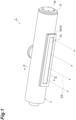
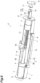
- An electron beam emission device (an energy beam emission device) 1 shown in FIG. 1 is used for, for example, ink curing, sterilizing, or surface reforming on an irradiation target by irradiating the irradiation target with electron beams (energy beams) EB.
- an electron beam emitting side (a side of a window 9) which is a side from which the electron beams EB are emitted by the electron beam emission device 1 will be described as a "front side.”
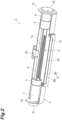
- the electron beam emission device 1 includes a filament unit (an electron discharge unit) 2, a vacuum container (a housing) 3, a cathode holding member 4, a cathode holding member 5, a rail (a unit accommodation part) 6, a high voltage introduction insulation member (a power supply part) 7, and an insulation support member 8.
- the filament unit 2 is an electron beam generation unit that generates the electron beams EB. Further, the filament unit 2 is a long unit.
- the vacuum container 3 is formed of a conductive material such as a metal.
- the vacuum container 3 has a substantially cylindrical shape.
- the vacuum container 3 forms a vacuum space R having a substantially circular column shape inside.
- the filament unit 2 is disposed inside the vacuum container 3 in an axial direction (a major axis direction) of the vacuum space R having a substantially circular column shape.
- An opening 3a through which the vacuum space R and an external space communicate with each other is provided at a position on the front side in the vacuum container 3 with respect to the filament unit 2.
- the vacuum container 3 includes a window 9 through which electrons discharged from the filament unit 2 pass. The window 9 is fixed to the opening 3a to be vacuum-sealed.
- the window 9 includes a window material 9a and a support 9b.
- the window material 9a is formed in a thin film shape.
- a material of the window material 9a a material having excellent transparency for the electron beams EB (for example, beryllium, titanium, aluminum, or the like) is used.
- the support 9b is disposed on a side of the vacuum space R of the window material 9a and supports the window material 9a.
- the support 9b is a mesh-like member and has a plurality of holes through which the electron beams EB pass.
- An exhaust port 3b for exhausting air in the vacuum container 3 is provided at a position on a rear side in the vacuum container 3 with respect to the filament unit 2.
- a vacuum pump (not shown) is connected to the exhaust port 3b, and the air in the vacuum container 3 is discharged by the vacuum pump. As a result, the inside of the vacuum container 3 becomes the vacuum space R.
- An opening 3c at the other end of the vacuum container 3 having a substantially cylindrical shape is closed by a flange 7a of the high voltage introduction insulation member 7.
- a housing end plate 3f is provided at one end of the vacuum container 3.
- the housing end plate 3f is provided with an insertion opening (an introduction opening) 3d (see FIG. 6 ) through which an inside space and an outside space of the vacuum container 3 communicate with each other.
- the insertion opening 3d has a size that allows the filament unit 2 to be introduced.
- the insertion opening 3d is closed by a lid 3e provided to be openable and closable (here, attachable and detachable) with respect to the housing end plate 3f.
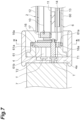
- a pair of cathode holding members 4 and 5 that have a cathode potential are disposed in the vacuum container 3.
- the rail 6 which has a cathode potential and also serves as a surrounding electrode that surrounds the filament unit 2 is provided between the cathode holding member 4 on the other side and the cathode holding member 5 on one side.
- the rail 6 is a conductive and long member having a substantially C-shaped cross section.
- the rail 6 is disposed such that an opening having a substantially C-shaped cross section faces the front side (a side of the window 9).
- the rail 6 holds the filament unit 2 in an inside portion (an internal space). In other words, the rail 6 has a long tubular shape capable of accommodating the filament unit 2.
- the rail 6 has an opening (an electron discharge opening) formed in a portion of an outer peripheral surface facing the window 9. Both ends of the rail 6 are fixed to the vacuum container 3 by the cathode holding member 4 and the high voltage introduction insulation member 7 and the cathode holding member 5 and the insulation support member 8.
- the insertion opening 3d of the housing end plate 3f faces one end (an end on a side fixed to the cathode holding member 5) of the rail 6.
- the filament unit 2 is inserted into the inside (an inside space) of the rail 6 from the one end of the rail 6 through the insertion opening 3d of the housing end plate 3f and insertion holes 5a and 8a (see FIG. 8 ) provided in the cathode holding member 5 and the insulation support member 8 in a state where the lid 3e of the vacuum container 3 is removed (opened).
- the filament unit 2 is held by the rail 6. In this way, the filament unit 2 can be inserted and removed (inserted to be attachable and detachable) with respect to the rail 6 from the one end of the rail 6.
- the high voltage introduction insulation member 7 supplies electric power to the filament unit 2.
- the high voltage introduction insulation member 7 is provided at an end of the vacuum container 3 on a side of the opening 3c on the other side. The other end of the high voltage introduction insulation member 7 projects to the outside of the vacuum container 3 through the opening 3c.
- the high voltage introduction insulation member 7 has the flange 7a protruding outward in a radial direction thereof and seals the opening 3c of the vacuum container 3.
- the high voltage introduction insulation member 7 is formed of an insulation material (for example, an insulation resin such as an epoxy resin, ceramic, or the like).
- the cathode holding member 4 holds one end of the high voltage introduction insulation member 7 in a state where the cathode holding member 4 is electrically insulated from the vacuum container 3 which has a ground potential.
- the high voltage introduction insulation member 7 is a high withstand voltage type connector for receiving supply of a high voltage from a power source device outside the electron beam emission device 1.
- a plug for supplying a high voltage from the power source device (not shown) is inserted into the high voltage introduction insulation member 7.
- An internal wiring for supplying a high voltage supplied from the outside to the filament unit 2 and the like is provided inside the high voltage introduction insulation member 7.
- This internal wiring is covered with an insulation material constituting the high voltage introduction insulation member 7, and insulation with respect to the vacuum container 3 is ensured.
- the one end disposed in the vacuum container 3 of the high voltage introduction insulation member 7 (the end on a side supporting the cathode holding member 4) faces the other end of the rail 6 (the end on a side fixed to the cathode holding member 4).
- the insulation support member 8 is provided at an end of the vacuum container 3 on a side where the housing end plate 3f on the one side is provided (an end on a side of the lid 3e).
- the insulation support member 8 is formed of an insulation material (for example, an insulation resin such as an epoxy resin, ceramic, or the like).
- the insulation support member 8 is supported by the housing end plate 3f.
- the cathode holding member 5 is supported by the insulation support member 8 in a state where the cathode holding member 5 is electrically insulated from the vacuum container 3.
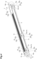
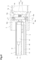
- the filament unit 2 is configured as one unit to be attachable to and detachable from the rail 6.
- the filament unit 2 includes a filament (an electron discharge part) 10, a main frame 11, a grid electrode 12, a sub frame 13, a power supply line 14, a guide member 15, a terminal holding member (a rotation restricting member) 16, a filament fixing member 17, a rotation restricting member 18, and a tension holding unit 19.
- the main frame 11 is a long member having a substantially U-shaped (C-shaped) cross section.
- the main frame 11 is disposed such that an opening having a substantially U-shaped cross section faces the front side (a side of the window 9).
- the filament fixing member 17 is provided at the other end of the main frame 11 in the inside (an inside space) of the main frame 11.
- the tension holding unit 19 is provided at one end of the main frame 11 in the inside (the inside space) of the main frame 11.
- the filament 10 is an electron discharge part that discharges electrons that become the electron beams EB when heated by energization.
- the filament 10 is a linear member and is a long member that extends on a desired axis L extending from one side to the other side.
- the filament 10 is formed of a metal material having a high melting point, for example, a material containing tungsten as a main component.
- One end of the filament 10 is connected to the tension holding unit 19.
- the other end of the filament 10 is connected to the filament fixing member 17.
- the terminal holding member 16 is attached to the other end of the main frame 11.
- the terminal holding member 16 holds a filament terminal T1 for supplying a current for the filament 10 to discharge electrons, a high voltage terminal T2 for supplying a cathode potential to the filament unit 2, and a grid electrode terminal T3 for supplying an applied voltage to the grid electrode 12 in a state where the terminals T1, T2, and T3 are electrically insulated from each other.
- the filament terminal T1 is connected to the other end of the power supply line 14.
- the high voltage terminal T2 is electrically connected to the filament fixing member 17.
- a guide groove (a groove) 16a extending in a direction of the axis L (an extending direction of the filament 10) is provided in an outer edge of the terminal holding member 16.
- the terminal holding member 16 is provided with two guide grooves 16a.
- the two guide grooves 16a are provided to face each other with the axis L interposed therebetween in the direction of the axis L.
- the filament unit 2 is inserted into the inside of the rail 6 from the one end of the rail 6 through the insertion opening 3d of the housing end plate 3f and insertion holes 5a and 8a provided in the cathode holding member 5 and the insulation support member 8 with the other end provided with the terminal holding member 16 as a head.
- the rotation restricting member 18 is attached to the one end of the main frame 11. That is, the filament fixing member 17 and the rotation restricting member 18 are provided at the positions of both ends of the filament unit 2.
- a guide groove (a groove) 18a extending in a direction of the axis L (an extending direction of the filament 10) is provided in an outer edge of the rotation restricting member 18.
- the rotation restricting member 18 is provided with two guide grooves 18a.
- the two guide grooves 18a are provided to face each other with the axis L interposed therebetween in the direction of the axis L.
- the guide groove 16a and the guide groove 18a are provided such that the guide groove 16a and the guide groove 18a overlap each other in the direction of the axis L.
- the sub frame 13 is a long member having a substantially U-shaped cross section.
- the sub frame 13 is disposed in parallel with the main frame 11.
- the power supply line 14 is connected to the tension holding unit 19 from a connection position with the filament terminal T1 through the inside (an inside space) of the sub frame 13, and the sub frame 13 has a protective function for the power supply line 14.
- the main frame 11 and the sub frame 13 are connected to each other by a plurality of guide members 15.
- the guide member 15 includes a first guide part 15a, a second guide part 15b, and a third guide part 15c.
- the first guide part 15a connects the main frame 11 and the sub frame 13 to each other at the other end of the filament unit 2 where the terminal holding member 16 is provided.
- the third guide part 15c connects the main frame 11 and the sub frame 13 to each other at the one end of the filament unit 2 where the rotation restricting member 18 is provided. In this way, the first guide part 15a and the third guide part 15c are provided at the positions of both ends of the filament unit 2.
- the second guide part 15b connects the main frame 11 and the sub frame 13 to each other at a position between the first guide part 15a and the third guide part 15c.
- a position of a center of the filament unit 2 in the extending direction is defined as a central position P.
- a portion on a side of the terminal holding member 16 with respect to the central position P (the other side: a tip end side in the insertion direction into the rail 6) is defined as a tip end side portion Y.
- the second guide part 15b is provided in the tip end side portion Y of the filament unit 2. That is, the tip end side portion Y is provided with the first guide part 15a and the second guide part 15b.
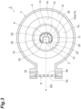
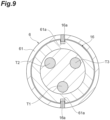
- a plurality of positioning parts 20 are provided on the outer surface of the first guide part 15a.
- the positioning part 20 is slidably in contact with the inner surface of the rail 6 to position the filament unit 2 with respect to the rail 6.
- the plurality of positioning parts 20 are provided on the outer surface of the first guide part 15a (the filament unit 2) in a circumferential direction of the filament unit 2.
- the circumferential direction of the filament unit 2 is a direction that orbits (rotates) around the filament unit 2 with the extending direction of the long filament unit 2 as an axis.
- Four positioning parts 20 are provided with respect to the first guide part 15a.
- the positioning part 20 includes a spherical body 20a and a holding part 20b.
- the spherical body 20a is in contact with the inner surface of the rail 6.
- the holding part 20b rotatably holds the spherical body 20a with respect to the first guide part 15a. Further, the holding part 20b holds the spherical body 20a in a state where a part of the spherical body 20a is exposed such that the spherical body 20a can be in contact with the inner surface of the rail 6.
- the second guide part 15b and the third guide part 15c are each provided with a plurality of positioning parts 20.
- the positioning part 20 provided in each of the second guide part 15b and the third guide part 15c has the same configuration as the positioning part 20 provided in the first guide part 15a, and detailed description thereof will be omitted.
- the positioning part 20 is provided in each of the first guide part 15a to the third guide part 15c, and thus a plurality of positioning parts 20 are provided in the extending direction of the filament 10. That is, the positioning part 20 is provided at each of a plurality of positions in the extending direction of the filament 10.
- the positioning part 20 is provided in each of the first guide part 15a and the third guide part 15c positioned at both ends of the filament unit 2. That is, the positioning part 20 is provided at each of the positions of both ends of the filament unit 2 on one side and the other side in the extending direction of the filament 10.
- the tip end side portion Y of the filament unit 2 is provided with the first guide part 15a and the second guide part 15b. That is, the filament unit 2 is provided with the positioning part 20 of the first guide part 15a and the positioning part 20 of the second guide part 15b at the plurality of positions in the extending direction of the filament unit 2 in the tip end side portion Y.
- the grid electrode 12 is disposed on the front side with respect to the filament 10 and is supported by the guide member 15 via an insulation member 22. A plurality of holes are formed in the grid electrode 12 (see FIG. 4 and the like). The grid electrode 12 is electrically connected to the grid electrode terminal T3 via a wiring (not shown).
- the tension holding unit 19 holds tension of the filament 10.
- the tension holding unit 19 can hold the tension of the filament 10 by pressing or pulling a movable body connected to the end of the filament 10 on the one side by a spring.
- the tension holding unit 19 is attached to the main frame 11 in a state where the tension holding unit 19 is electrically insulated from the main frame 11 via an insulation member or the like.
- One end of the power supply line 14 is connected to the tension holding unit 19.
- the tension holding unit 19 can supply the electric power supplied via the power supply line 14 to the filament 10 while holding the tension of the filament 10.
- the filament unit 2 is inserted into the inside (the inside space) of the rail 6 through the insertion opening 3d of the housing end plate 3f, the insertion hole 8a provided in the insulation support member 8, and the insertion hole 5a provided in the cathode holding member 5 with the other end provided with the terminal holding member 16 as a head and is fixed thereto.
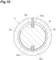
- the rail 6 includes a surrounding part 60, a first annular part 61, and a second annular part 62 as shown in FIGS. 7 and 8 .
- the surrounding part 60 surrounds a portion of the filament unit 2 provided with the filament 10.
- the surrounding part 60 is a long member having a substantially C-shaped cross section.
- the first annular part 61 is connected to the other end of the surrounding part 60.
- the end of the rail 6 on a side of the first annular part 61 (the other side) is fixed to the cathode holding member 4.
- the cathode holding member 4 has a tubular shape to surround the other end of the rail 6 provided with the first annular part 61.
- the second annular part 62 is connected to one end of the surrounding part 60.
- the end of the rail 6 on a side of the second annular part 62 (the one side) is fixed to the cathode holding member 5.
- the cathode holding member 5 has a tubular shape to surround the one end of the rail 6 provided with the second annular part 62.
- the first annular part 61 has a contact surface 61b facing one side, that is, a side of the insertion opening 3d of the housing end plate 3f (a side of the surrounding part 60).
- the contact surface 61b comes into contact with the other tip end surface of the filament unit 2 (the other end surface of the terminal holding member 16). Therefore, in the contact surface 61b, an insertion depth of the filament unit 2 can be determined.
- a position of the filament unit 2 in a state where the tip end surface of the filament unit 2 is in contact with the contact surface 61b is defined as an insertion completion position.
- the high voltage introduction insulation member 7 is in contact with the filament unit 2 in a state where the filament unit 2 is inserted into the rail 6 to the insertion completion position and is electrically connected to the filament unit 2.
- connection terminals T for supplying electric power to the filament unit 2 are provided on a surface of the high voltage introduction insulation member 7 on a side of the rail 6 (the one side).
- the connection terminal T passes through a through hole provided in a wall 4a of the cathode holding member 4 not to come into contact with the cathode holding member 4 and is exposed on a side of the rail 6 (the one side).
- tip ends of the filament terminal T1, the high voltage terminal T2, and the grid electrode terminal T3 are in contact with tip ends of three connection terminals provided in the high voltage introduction insulation member 7.
- the filament terminal T1 and the like are electrically connected to the connection terminals T of the high voltage introduction insulation member 7.
- the filament terminal T1 may be configured to be elastically deformable in an insertion direction of the filament unit 2.
- the filament terminal T1 can be more reliably in contact with the connection terminal T and electrically connected thereto.
- an end surface of the filament terminal T1 and an end surface of the connection terminal T are in contact with each other. Therefore, even if a center position of the filament terminal T1 and a center position of the connection terminal T are misaligned, as long as the end surfaces are in contact with each other, the filament terminal T1 and the connection terminal T are electrically connected to each other.
- the filament terminal T1 can absorb the variation in the projection length by elastically deforming and thus can come into contact with the connection terminal T. Further, an impact occurring when the filament unit 2 is inserted and the filament terminal T1 and the connection terminal T come into contact with each other can be alleviated by the elastic deformation of the filament terminal T1.
- the high voltage terminal T2 and the grid electrode terminal T3 may be configured to be elastically deformable in the insertion direction of the filament unit 2. Similar to the filament terminal T1 and the like, the connection terminal T may be configured to be elastically deformable in the insertion direction of the filament unit 2.
- the first annular part 61 surrounds the terminal holding member 16 in a state where the tip end surface of the filament unit 2 is in contact with the contact surface 61b.
- the cathode holding member 4 is not shown.
- the first annular part 61 is provided with a guide projection (a projection) 61a that projects from the outer surface side (the outer peripheral side) of the first annular part 61 (the rail 6) toward the inner surface side (the inside) of the first annular part 61 (the rail 6).
- the first annular part 61 is provided with two guide projections 61a.
- the two guide projections 61a are provided to face each other with the axis L interposed therebetween in the direction of the axis L.
- the guide projection 61a of the first annular part 61 is fitted into the guide groove 16a of the terminal holding member 16 provided at the tip end of the filament unit 2.
- a position in a rotation direction (an orientation) with the extending direction of the filament unit 2 in the rail 6 as an axis is determined.
- the second annular part 62 surrounds the rotation restricting member 18 in a state where the tip end surface of the filament unit 2 is in contact with the contact surface 61b.
- the cathode holding member 5 is not shown.
- the second annular part 62 is provided with a guide projection (a projection) 62a that projects from the outer surface side (the outer peripheral side) of the second annular part 62 (the rail 6) toward the inner surface side (the inside) of the second annular part 62 (the rail 6).
- the second annular part 62 is provided with two guide projections 62a.
- the two guide projections 62a are provided to face each other with the axis L interposed therebetween in the direction of the axis L. In this way, the guide projection 61a and the guide projection 62a are provided at the positions of both ends of the rail 6. In the present embodiment, the guide projection 61a and the guide projection 62a are provided such that the guide projection 61a and the guide projection 62a overlap each other in the direction of the axis L.
- the guide projection 62a of the second annular part 62 is fitted into the guide groove 18a of the rotation restricting member 18 provided in the filament unit 2. As a result, a position in a rotation direction (an orientation) with the extending direction of the filament unit 2 in the rail 6 as an axis is determined.
- a unit pressing part 21 is attached to the insertion hole 5a of the cathode holding member 5 in a state where the filament unit 2 is inserted into the rail 6.
- the unit pressing part 21 includes a fixing part 21a and a pressing member 21b.
- the fixing part 21a is detachably attached to the cathode holding member 5 to cover the insertion hole 5a of the cathode holding member 5.
- the pressing member 21b is attached to a surface of the other side of the fixing part 21a which is a side of the filament unit 2 (a side of the rail 6).
- the pressing member 21b presses the filament unit 2 toward the other side which is a deep side in the insertion direction (a side of the cathode holding member 4).
- the pressing member 21b is, for example, a compression spring.
- the unit pressing part 21 press the filament unit 2, a state in which the tip end surface of the filament unit 2 is in contact with the contact surface 61b of the first annular part 61 is maintained.
- the unit pressing part 21 is not limited to being attached to the cathode holding member 5 and may be detachably attached to the insulation support member 8 or detachably attached to the housing end plate 3f.
- the filament 10 discharges electrons when a high negative voltage such as minus several tens of kV to minus several hundreds of kV is applied in a state where the filament 10 is heated by energization in a state where the filament unit 2 is inserted into the rail 6 to the insertion completion position.
- a predetermined voltage is applied to the grid electrode 12.
- a voltage on a positive side of about 100 V to 150 V with respect to the negative voltage applied to the filament 10 may be applied to the grid electrode 12.
- the grid electrode 12 forms an electric field for drawing out electrons and curbing diffusion of the electrons. As a result, the electrons discharged from the filament 10 are emitted to the front side as the electron beams EB from the holes provided in the grid electrode 12.
- the electron beam emission device 1 is installed such that the window 9 faces in a horizontal direction, for example, in a case where the electron beams EB are emitted in the horizontal direction. Further, the electron beam emission device 1 is installed such that the window 9 faces downward, for example, in a case where the electron beams EB are emitted downward. In this way, an orientation of the installation of the electron beam emission device 1 is determined according to an orientation of the emission of the electron beams EB. Even in a case where the electron beam emission device 1 is installed in various directions, the filament unit 2 can be stably disposed by the rail 6.
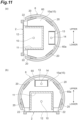
- the four positioning parts 20 are provided on the outer surface of the first guide part 15a at predetermined intervals in the circumferential direction of the filament unit 2. Further, as shown in FIG. 11(a) , in a case where the electron beams EB are emitted from the filament unit 2 in the horizontal direction, the four positioning parts 20 provided in the first guide part 15a are provided such that two positioning parts 20 are positioned on a surface facing downward in the guide member 15 (the filament unit 2).
- the surface facing downward includes not only a surface facing directly downward but also a surface facing diagonally downward. That is, the surface facing downward is a surface facing downward rather than in the horizontal direction. As a result, even in a case where the filament unit 2 is affected by gravity, the two positioning parts 20 provided on the surface facing downward are in contact with the inner surface 60a of the surrounding part 60 of the rail 6.
- the four positioning parts 20 provided in the first guide part 15a are provided such that two positioning parts 20 are positioned on a surface facing downward in the guide member 15 (the filament unit 2).
- the two positioning parts 20 provided on the surface facing downward are in contact with the inner surface 60a of the surrounding part 60 of the rail 6.
- the four positioning parts 20 provided in the first guide part 15a are provided such that two positioning parts 20 are positioned on a surface facing downward in the guide member 15 (the filament unit 2).
- the filament unit 2 is disposed in a stable state with respect to the rail 6 by the two positioning parts 20 provided on the surface facing downward in the first guide part 15a.
- the second guide part 15b and the third guide part 15c also have the same arrangement configuration of the positioning parts 20 as the first guide part 15a.
- the electron beam emission device 1 may be disposed to emit the electron beams EB in various directions such as a diagonally downward direction and a diagonally upward direction without being limited to the cases where the electron beams EB are emitted in the horizontal direction, the direct downward direction, and the direct upward direction. Even in this case, it is sufficient that two positioning parts 20 are provided on the surface facing downward for each of the first guide part 15a to the third guide part 15c.
- the plurality of positioning parts 20 provided in the first guide part 15a are disposed such that two or more positioning parts 20 are provided on a surface facing downward in the first guide part 15a (the filament unit 2). Further, in a state where the filament unit 2 is disposed to emit the electron beams EB toward a second direction different from the first direction, the plurality of positioning parts 20 provided in the first guide part 15a are disposed such that two or more positioning parts 20 are provided on a surface facing downward in the first guide part 15a (the filament unit 2).
- the positioning parts 20 provided in each of the second guide part 15b and the third guide part 15c also have the same arrangement as the positioning parts 20 provided in the first guide part 15a.
- the maximum interval between the positioning parts 20 in the circumferential direction of the filament unit 2 is shorter than a half circumference.
- the interval between the positioning parts 20 provided in each of the second guide part 15b and the third guide part 15c is also the same as that between the positioning parts 20 provided in the first guide part 15a.
- the four positioning parts 20 provided in the first guide part 15a may be provided line-symmetrically with respect to a desired reference line or point-symmetrically with respect to a predetermined reference point in the extending direction of the filament 10.
- the positioning parts 20 provided in each of the second guide part 15b and the third guide part 15c may also have the same arrangement as the positioning parts 20 provided in the first guide part 15a.
- the plurality of positioning parts 20 that are slidably in contact with the inner surface 60a of the rail 6 are provided between the outer surface of the filament unit 2 and the inner surface 60a of the rail 6. That is, the long filament unit 2 is disposed in the rail 6 by being supported at a plurality of positions where the positioning parts 20 are provided.
- the positioning part 20 of the filament unit 2 is easily brought into contact with the inner surface 60a of the rail 6 as compared with, for example, a case where the entire lower surface of the filament unit 2 is brought into contact with a bottom surface of the rail 6.
- the filament unit 2 since the filament unit 2 has the plurality of positioning parts 20, the filament unit 2 can be held by the rail 6 while the positioning of the filament unit 2 with respect to the rail 6 is performed. As described above, in the electron beam emission device 1, it is possible to stably dispose the filament unit 2 even if the filament unit 2 has a long shape.
- connection terminals T provided in the high voltage introduction insulation member 7 are in contact with the filament terminal T1 to the grid electrode terminal T3 of the filament unit 2 in a state where the filament unit 2 is inserted into the rail 6 to the insertion completion position and are electrically connected thereto.
- the electron beam emission device 1 it is possible to electrically connect the filament unit 2 and the high voltage introduction insulation member 7 to each other by performing work of disposing the filament unit 2 in the rail 6 (work of inserting the filament unit 2 into the rail 6) without performing special work for connecting the filament unit 2 and the connection terminal T of the high voltage introduction insulation member 7.
- the insertion opening 3d which is opened and closed by the lid 3e is provided at a portion of the vacuum container 3 facing the one end of the rail 6.
- the filament unit 2 can be attached to and detached from the one end of the rail6 via the insertion opening 3d of the vacuum container 3.
- the positioning part 20 includes the spherical body 20a.
- the filament unit 2 can smoothly slide in the rail 6 by the spherical body 20a of the positioning part 20 being rotated.
- the electron beam emission device 1 it is possible to easily attach and detach the filament unit 2 to and from the rail 6.
- the positioning part 20 is provided in each of the first guide part 15a to the third guide part 15c provided in the extending direction of the filament 10. That is, the plurality of positioning parts 20 are provided in the extending direction of the filament 10. In this case, in the electron beam emission device 1, it is possible to curb the filament unit 2 being slantwise accommodated with respect to the extending direction of the rail 6, and it is possible to stably dispose the filament unit 2.
- the positioning part 20 is provided at each of both ends of the filament unit 2. In this case, in the electron beam emission device 1, it is possible to further curb the filament unit 2 being slantwise accommodated with respect to the extending direction of the rail 6, and it is possible to further stably dispose the filament unit 2.
- the tip end side portion Y of the filament unit 2 is provided with the first guide part 15a and the second guide part 15b each including the positioning part 20.
- the positioning parts 20 of the first guide part 15a and the second guide part 15b disposed in the tip end side portion Y on the tip end side in the insertion direction into the rail 6 come into contact with the inner surface 60a of the rail 6 at an early stage of insertion. That is, in the electron beam emission device 1, when the long filament unit 2 is inserted, the filament unit 2 is positioned with respect to the rail 6 at the early stage.
- the electron beam emission device 1 it is possible to stably attach and detach the filament unit 2 to and from the rail 6 even in a case where the filament unit 2 has a long shape. Further, it is possible to curb the filament unit 2 being inserted in an inclined state, and it is possible to curb the filament unit 2 buffering to other parts.
- the plurality of positioning parts 20 are provided on the outer surface of the filament unit 2 in the circumferential direction of the filament unit 2. In this case, in the electron beam emission device 1, it is possible to stabilize the position of the filament unit 2 in the rail 6 in a direction orthogonal to the extending direction of the filament unit 2.
- the guide projection 61a provided in the first annular part 61 of the rail 6 is fitted into the guide groove 16a of the terminal holding member 16 provided at the end of the filament unit 2. Further, the guide projection 62a provided in the second annular part 62 of the rail 6 is fitted into the guide groove 18a of the rotation restricting member 18 provided at the end of the filament unit 2.
- the position (the orientation) of the filament unit 2 in the rotation direction when seen in the extending direction of the filament unit 2 can be determined by the guide grooves 16a and 18a and the guide projections 61a and 62a.
- the guide grooves 16a and 18a are provided at both ends of the filament unit 2.
- the guide projections 61a and 62a are provided at both ends of the rail 6.
- the position of the filament unit 2 in the rotation direction at both ends of the filament unit 2 can be determined, and the filament unit 2 can be stably disposed.
- the guide projections 61a and the guide groove 16a on the deep side in the insertion direction (the other side) may not be visible to the operator.
- the guide projection 62a is fitted into the guide groove 18a on the front side (the one side) in the insertion direction
- the guide projection 61a is also fitted into the guide groove 16a on the deep side in the insertion direction.
- the electron beam emission device 1 has a configuration in which the guide grooves 16a and 18a are provided at both ends of the filament unit 2 for determining the positions in the rotation direction, the filament unit 2 can be easily inserted into the rail 6 and disposed therein.
- the positioning part 20 is not limited to the case where it is provided on the outer surface of the filament unit 2 and may be provided on the inner surface 60a of the rail 6. In this case, the positioning part 20 comes into contact with the outer surface of the filament unit 2. Further, the positioning part 20 is not limited to the configuration including the spherical body 20a.
- the outer surface of the positioning part 20 may be a protrusion having a protruding curved surface shape.
- the filament unit 2 can slide smoothly with respect to the inner surface 60a of the rail 6 while curbing the protrusion having the protruding curved surface shape, which is the positioning part, being caught.
- the positioning part 20 is a protrusion
- the outer surface of the positioning part 20 does not have to be in a protruding curved surface shape.
- the positioning part 20 is not limited to being provided on the outer surface of the guide member 15.
- the positioning part 20 may be provided directly on the outer surface of the rail 6 or the like.
- the guide member 15 has three guide parts like the first guide part 15a to the third guide part 15c, but the number of guide parts is not limited to three. Further, the number of positioning parts 20 provided in one guide part is not limited to four.
- the guide projections 61a and 62a for determining the position of the filament unit 2 in the rotation direction are not limited to being provided at both ends of the rail 6.
- one or a plurality of guide projections may be provided at positions between both ends of the rail 6 in addition to both ends of the rail 6, or the guide projections may be provided on the rail 6 as a whole in the extending direction of the rail 6. In this case, the position of the filament unit 2 in the rotation direction is determined even in the middle of being inserted into the rail 6.
- the rail 6 is provided with the guide projections 61a and 62a, and the filament unit 2 is provided with the guide grooves 16a and 18a, but the present disclosure is not limited thereto.
- the rail 6 may be provided with the guide groove, and the filament unit 2 may be provided with the guide projection.
- a method of supplying electric power from the high voltage introduction insulation member 7 to the filament unit 2 is not limited to a method using the filament terminal T1 to the grid electrode terminal T3.
- the insulation support member 8 does not have to be fixed to the housing end plate 3f.
- one end of the insulation support member 8 may be fixed to the inner peripheral surface of the cylindrical portion of the vacuum container 3, and the other end of the insulation support member 8 may fix the cathode holding member 5.
- the surrounding part 60 of the rail 6 is not limited to a shape having a substantially C-shaped cross section.
- the surrounding part 60 may have a polygonal cross section.
- the shape of the guide member 15 is not limited to the shape described above and may be a shape corresponding to the surrounding part 60.
- the electron beam emission device 1 as the energy beam emission device may be configured as an X-ray emission device that emits X-rays.
- the electron beam emission device 1 includes an X-ray target (for example, tungsten, molybdenum, or the like) which is an X-ray generation part that generates X-rays when the electron beams EB discharged from the filament unit 2 are incident and can emit X-rays generated by the X-ray target from the window 9.
- a window for X-ray emission constituted by a window material having a high X-ray permeability (for example, beryllium, diamond, or the like) and the X-ray target provided on a surface of the window material on a side of the vacuum space R.
- a window material having a high X-ray permeability for example, beryllium, diamond, or the like
- the electron beams EB emitted from the filament unit 2 can be incident on the X-ray target, and the X-rays can be emitted from the X-ray target.
Landscapes
- Physics & Mathematics (AREA)
- Engineering & Computer Science (AREA)
- General Engineering & Computer Science (AREA)
- High Energy & Nuclear Physics (AREA)
- Electron Sources, Ion Sources (AREA)
- X-Ray Techniques (AREA)
Claims (12)
- Elektronenstrahl-Emissionsvorrichtung, die umfasst:eine Filament-Einheit (2), die so ausgeführt ist, dass sie Elektronen ausstößt, wobei die Filament-Einheit (2) eine lange Einheit ist;ein Gehäuse (3) mit einem Fenster, durch das von der Filament-Einheit (2) ausgestoßene Elektronen hindurchtreten; undeinen Einheit-Aufnahmeteil (6), der in dem Gehäuse (3) befestigt ist, die Form einer langen Röhre hat, die einen Abschnitt der Filament-Einheit (2) umschließt und die Filament-Einheit (2) hält, wobei der Einheit-Aufnahmeteil (6) eine Elektronen-Ausstoßöffnung aufweist, die in einem dem Fenster zugewandten Abschnitt einer Außenumfangsfläche ausgebildet ist,wobei eine Vielzahl von Positionierteilen (20) zwischen einer Außenfläche der Filament-Einheit (2) und einer Innenfläche des Einheit-Aufnahmeteils (6) vorhanden sind, die Positionierteile (20) in Gleitkontakt mit der Außenfläche der Filament-Einheit (2) oder der Innenfläche des Einheit-Aufnahmeteils (6) sind und Positionieren der Filament-Einheit (2) in Bezug auf den Einheit-Aufnahmeteil (6) durchführen, undwobei die Filament-Einheit (2) über ein Ende des Einheit-Aufnahmeteils (6) in den Einheit-Aufnahmeteil (6) eingeführt werden kann.
- Elektronenstrahl-Emissionsvorrichtung nach Anspruch 1, die des Weiteren umfasst:einen Strom-Zuführteil (7), der so ausgeführt ist, dass er der Filament-Einheit (2) elektrischen Strom zuführt,wobei der Strom-Zuführteil (7) in dem Gehäuse (3) an der anderen Endseite des Einheit-Aufnahmeteils (6) vorhanden ist und so in Kontakt mit der Filament-Einheit (2) ist,dass er in einem Zustand elektrisch mit der Filament-Einheit (2) verbunden ist, in dem die Filament-Einheit (2) in den Einheit-Aufnahmeteil (6) eingeführt ist.
- Elektronenstrahl-Emissionsvorrichtung nach Anspruch 2, wobei das eine Ende des Gehäuses (3) mit einer Einführungsöffnung (3d) versehen ist, in die die Filament-Einheit (2) eingeführt werden kann und die mit einer Klappe (3e) geöffnet und geschlossen wird.
- Elektronenstrahl-Emissionsvorrichtung nach einem der Ansprüche 1 bis 3, wobei eine Außenfläche des Positionierteils (20) der Vielzahl von Positionierteilen die Form einer vorstehenden gekrümmten Fläche hat.
- Elektronenstrahl-Emissionsvorrichtung nach einem der Ansprüche 1 bis 3, wobei der Positionierteil (20) der Vielzahl von Positionierteilen einen sphärischen Körper (20a), der in Kontakt mit der Außenfläche der Filament-Einheit (2) oder der Innenfläche des Einheit-Aufnahmeteils (6) ist, sowie einen Halteteil (20b) enthält, der den sphärischen Körper (20a) drehbar hält.
- Elektronenstrahl-Emissionsvorrichtung nach einem der Ansprüche 1 bis 5, wobei die Filament-Einheit (2) ein Filament (10) enthält und die Vielzahl von Positionierteilen (20) in einer Erstreckungsrichtung des Filaments (10) vorhanden sind.
- Elektronenstrahl-Emissionsvorrichtung nach einem der Ansprüche 1 bis 6, wobei die Filament-Einheit (2) ein Filament (10) enthält, und ein Positionierteil (20) der Vielzahl von Positionierteilen an jedem von beiden Enden an einer Seite und der anderen Seite in einer Erstreckungsrichtung des Filaments (10) vorhanden ist.
- Elektronenstrahl-Emissionsvorrichtung nach einem der Ansprüche 1 bis 7, wobei die Filament-Einheit (2) ein Filament (10) enthält, und ein Positionierteil (20) der Vielzahl von Positionierteilen an der Außenfläche der Filament-Einheit (2) vorhanden ist und an jeder einer Vielzahl von Positionen in einer Erstreckungsrichtung des Filaments (10) an einer Position an der Seite eines vorderen Endes in einer Richtung für Einführung in den Einheit-Aufnahmeteil (6) in Bezug auf eine Mittelposition in der Erstreckungsrichtung des Filaments (10) vorhanden ist.
- Elektronenstrahl-Emissionsvorrichtung nach einem der Ansprüche 1 bis 8, wobei die Vielzahl von Positionierteilen (20) in einer Umfangsrichtung der Filament-Einheit (2) vorhanden sind.
- Elektronenstrahl-Emissionsvorrichtung nach einem der Ansprüche 1 bis 9, die des Weiteren umfasst:einen Vorsprung (61a, 62a), der von einer Seite der Außenfläche des Einheit-Aufnahmeteils (6) in Richtung einer Seite der Innenfläche des Einheit-Aufnahmeteils (6) vorsteht,wobei die Filament-Einheit (2) des Weiteren ein Filament (10) sowie ein Drehungs-Einschränkungselement (16,18) aufweist, in dem eine Nut (16a, 18a), die in einer Erstreckungsrichtung des Filaments (10) verläuft, in einem äußeren Rand ausgebildet ist, undwobei eine Position der Filament-Einheit (2) in einer Drehungsrichtung in dem Einheit-Aufnahmeteil (6) durch den Vorsprung (61a, 62a) bestimmt wird, der in die Nut (16a, 18a) eingepasst ist.
- Elektronenstrahl-Emissionsvorrichtung nach Anspruch 10,wobei der Vorsprung (61a, 62a) an jeder von beiden Endseiten des Einheit-Aufnahmeteils (6) vorhanden ist, undwobei das Drehungs-Einschränkungselement (16, 18) an jeder von beiden Endseiten der Filament-Einheit (2) vorhanden ist.
- Röntgenstrahl-Emissionsvorrichtung, die umfasst:
eine Filament-Einheit (2), die so ausgeführt ist, dass sie Elektronen ausstößt, wobei die Filament-Einheit (2) eine lange Einheit ist; ein Gehäuse (3) mit einem Fenster, über das die Röntgenstrahlen emittiert werden; und einen Einheit-Aufnahmeteil (6), der in dem Gehäuse (3) befestigt ist, eine lange Röhrenform hat, die einen Abschnitt der Filament-Einheit (2) umschließt und die Filament-Einheit (2) hält, wobei der Einheit-Aufnahmeteil (6) eine Elektronen-Ausstoßöffnung aufweist, die in einem dem Fenster zugewandten Abschnitt einer Außenumfangsfläche ausgebildet ist, wobei eine Vielzahl von Positionierteilen (20) zwischen einer Außenfläche der Filament-Einheit (2) und einer Innenfläche des Einheit-Aufnahmeteils (6) vorhanden sind, die Positionierteile (20) in Gleitkontakt mit der Außenfläche der Filament-Einheit (2) oder der Innenfläche des Einheit-Aufnahmeteils (6) sind und Positionieren der Filament-Einheit (2) in Bezug auf den Einheit-Aufnahmeteil (6) durchführen, und wobei die Filament-Einheit (2) über ein Ende des Einheit-Aufnahmeteils (6) in den Einheit-Aufnahmeteil (6) eingeführt werden kann, wobei sie des Weiteren umfasst:
einen Röntgenstrahl-Erzeugungsteil, der so ausgeführt ist, dass er Röntgenstrahlen erzeugt, wenn die von der Filament-Einheit (2) ausgestoßenen Elektronen so auftreffen, dass die Röntgenstrahl-Emissionsvorrichtung Röntgenstrahlen über das Fenster (9) emittieren kann.
Applications Claiming Priority (2)
| Application Number | Priority Date | Filing Date | Title |
|---|---|---|---|
| JP2020071472A JP7434041B2 (ja) | 2020-04-13 | 2020-04-13 | エネルギー線照射装置 |
| PCT/JP2021/003091 WO2021210239A1 (ja) | 2020-04-13 | 2021-01-28 | エネルギー線照射装置 |
Publications (3)
| Publication Number | Publication Date |
|---|---|
| EP4131322A1 EP4131322A1 (de) | 2023-02-08 |
| EP4131322A4 EP4131322A4 (de) | 2024-06-19 |
| EP4131322B1 true EP4131322B1 (de) | 2025-01-08 |
Family
ID=78079632
Family Applications (1)
| Application Number | Title | Priority Date | Filing Date |
|---|---|---|---|
| EP21787645.7A Active EP4131322B1 (de) | 2020-04-13 | 2021-01-28 | Vorrichtung zur bestrahlung mit energiestrahlen |
Country Status (5)
| Country | Link |
|---|---|
| US (1) | US12444518B2 (de) |
| EP (1) | EP4131322B1 (de) |
| JP (2) | JP7434041B2 (de) |
| CN (1) | CN115398564A (de) |
| WO (1) | WO2021210239A1 (de) |
Family Cites Families (15)
| Publication number | Priority date | Publication date | Assignee | Title |
|---|---|---|---|---|
| JP2001021700A (ja) | 1999-07-07 | 2001-01-26 | Nissin High Voltage Co Ltd | 電子線照射装置 |
| JP3891800B2 (ja) | 2001-06-28 | 2007-03-14 | 独立行政法人科学技術振興機構 | 飛翔体発射装置 |
| JP2003149398A (ja) * | 2001-11-07 | 2003-05-21 | Mitsubishi Heavy Ind Ltd | 長尺低エネルギ電子線照射装置 |
| KR100577473B1 (ko) | 2004-03-09 | 2006-05-10 | 한국원자력연구소 | 전계방출팁을 이용한 저에너지 대면적 전자빔 조사장치 |
| JP2005300327A (ja) | 2004-04-12 | 2005-10-27 | Iwasaki Electric Co Ltd | 電子線照射装置 |
| US7672048B2 (en) * | 2004-11-27 | 2010-03-02 | Japan Advanced Instituter of Science and Technology | Positioning mechanism and microscope using the same |
| US7902529B2 (en) | 2007-08-02 | 2011-03-08 | Thermo Finnigan Llc | Method and apparatus for selectively providing electrons in an ion source |
| JP5193594B2 (ja) * | 2007-12-28 | 2013-05-08 | 東芝Itコントロールシステム株式会社 | X線検査装置 |
| CN102884222B (zh) | 2010-06-28 | 2014-09-10 | 日本爱发科泰克能株式会社 | 靶安装机构 |
| WO2013004562A1 (en) | 2011-07-04 | 2013-01-10 | Tetra Laval Holdings & Finance S.A. | Cathode housing suspension of an electron beam device |
| US9202661B2 (en) | 2011-07-04 | 2015-12-01 | Tetra Laval Holdings & Finance S.A. | Electron beam device for shaping an electric field and a method of manufacturing said electron beam device the same |
| JP2013098090A (ja) * | 2011-11-02 | 2013-05-20 | Fujifilm Corp | X線照射装置及びx線照射方法 |
| EP3240010B1 (de) | 2014-12-25 | 2022-02-09 | Meidensha Corporation | Feldemissionsvorrichtung und reformierungsbehandlungsverfahren |
| JP2018048828A (ja) | 2016-09-20 | 2018-03-29 | 岩崎電気株式会社 | 照射装置 |
| CN206907734U (zh) | 2017-06-30 | 2018-01-19 | 同方威视技术股份有限公司 | X射线管 |
-
2020
- 2020-04-13 JP JP2020071472A patent/JP7434041B2/ja active Active
-
2021
- 2021-01-28 CN CN202180028044.3A patent/CN115398564A/zh active Pending
- 2021-01-28 EP EP21787645.7A patent/EP4131322B1/de active Active
- 2021-01-28 WO PCT/JP2021/003091 patent/WO2021210239A1/ja not_active Ceased
- 2021-01-28 US US17/918,153 patent/US12444518B2/en active Active
-
2024
- 2024-02-07 JP JP2024017082A patent/JP7549168B2/ja active Active
Also Published As
| Publication number | Publication date |
|---|---|
| EP4131322A1 (de) | 2023-02-08 |
| JP2024036604A (ja) | 2024-03-15 |
| EP4131322A4 (de) | 2024-06-19 |
| JP2021167783A (ja) | 2021-10-21 |
| WO2021210239A1 (ja) | 2021-10-21 |
| US20230134054A1 (en) | 2023-05-04 |
| JP7549168B2 (ja) | 2024-09-10 |
| CN115398564A (zh) | 2022-11-25 |
| US12444518B2 (en) | 2025-10-14 |
| JP7434041B2 (ja) | 2024-02-20 |
Similar Documents
| Publication | Publication Date | Title |
|---|---|---|
| US8110974B2 (en) | Electron beam generating apparatus | |
| US10825640B2 (en) | X-ray tube | |
| EP1437757B1 (de) | Röntgenröhre und verfahren zu ihrer herstellung | |
| US20240363303A1 (en) | Cathode assembly for electron gun | |
| EP4131322B1 (de) | Vorrichtung zur bestrahlung mit energiestrahlen | |
| US11147148B2 (en) | X-ray generator | |
| JP2010015989A (ja) | 回転陽極型x線発生器における電子源の迅速な交換のための陰極アセンブリ | |
| WO2007105389A1 (ja) | 電子銃、エネルギー線発生装置、電子線発生装置、及びx線発生装置 | |
| US12176175B2 (en) | Electron beam generation source, electron beam emission device, and x-ray emission device | |
| KR102556786B1 (ko) | 전계 방사 장치 및 전계 방사 방법 | |
| US20230147125A1 (en) | Electron beam generator, electron beam emission device and x-ray emission device | |
| EP4254465B1 (de) | Quelle für geladene teilchenstrahlen und system für geladene teilchenstrahlen | |
| JP2021189038A (ja) | 電子線照射装置及び電子線照射装置の製造方法 | |
| KR101163513B1 (ko) | 광 이온 발생 장치 | |
| US20200335296A1 (en) | Reflection type x-ray tube |
Legal Events
| Date | Code | Title | Description |
|---|---|---|---|
| STAA | Information on the status of an ep patent application or granted ep patent |
Free format text: STATUS: THE INTERNATIONAL PUBLICATION HAS BEEN MADE |
|
| PUAI | Public reference made under article 153(3) epc to a published international application that has entered the european phase |
Free format text: ORIGINAL CODE: 0009012 |
|
| STAA | Information on the status of an ep patent application or granted ep patent |
Free format text: STATUS: REQUEST FOR EXAMINATION WAS MADE |
|
| 17P | Request for examination filed |
Effective date: 20221102 |
|
| AK | Designated contracting states |
Kind code of ref document: A1 Designated state(s): AL AT BE BG CH CY CZ DE DK EE ES FI FR GB GR HR HU IE IS IT LI LT LU LV MC MK MT NL NO PL PT RO RS SE SI SK SM TR |
|
| DAV | Request for validation of the european patent (deleted) | ||
| DAX | Request for extension of the european patent (deleted) | ||
| RIC1 | Information provided on ipc code assigned before grant |
Ipc: H05G 1/00 20060101ALI20240305BHEP Ipc: G21K 5/04 20060101ALI20240305BHEP Ipc: G21K 5/02 20060101ALI20240305BHEP Ipc: G21K 5/00 20060101ALI20240305BHEP Ipc: H01J 35/18 20060101ALI20240305BHEP Ipc: H01J 35/08 20060101ALI20240305BHEP Ipc: H01J 35/06 20060101ALI20240305BHEP Ipc: H01J 35/00 20060101AFI20240305BHEP |
|
| A4 | Supplementary search report drawn up and despatched |
Effective date: 20240521 |
|
| RIC1 | Information provided on ipc code assigned before grant |
Ipc: H05G 1/00 20060101ALI20240514BHEP Ipc: G21K 5/04 20060101ALI20240514BHEP Ipc: G21K 5/02 20060101ALI20240514BHEP Ipc: G21K 5/00 20060101ALI20240514BHEP Ipc: H01J 35/18 20060101ALI20240514BHEP Ipc: H01J 35/08 20060101ALI20240514BHEP Ipc: H01J 35/06 20060101ALI20240514BHEP Ipc: H01J 35/00 20060101AFI20240514BHEP |
|
| GRAP | Despatch of communication of intention to grant a patent |
Free format text: ORIGINAL CODE: EPIDOSNIGR1 |
|
| STAA | Information on the status of an ep patent application or granted ep patent |
Free format text: STATUS: GRANT OF PATENT IS INTENDED |
|
| INTG | Intention to grant announced |
Effective date: 20240930 |
|
| GRAS | Grant fee paid |
Free format text: ORIGINAL CODE: EPIDOSNIGR3 |
|
| GRAA | (expected) grant |
Free format text: ORIGINAL CODE: 0009210 |
|
| STAA | Information on the status of an ep patent application or granted ep patent |
Free format text: STATUS: THE PATENT HAS BEEN GRANTED |
|
| AK | Designated contracting states |
Kind code of ref document: B1 Designated state(s): AL AT BE BG CH CY CZ DE DK EE ES FI FR GB GR HR HU IE IS IT LI LT LU LV MC MK MT NL NO PL PT RO RS SE SI SK SM TR |
|
| REG | Reference to a national code |
Ref country code: GB Ref legal event code: FG4D |
|
| REG | Reference to a national code |
Ref country code: CH Ref legal event code: EP |
|
| REG | Reference to a national code |
Ref country code: DE Ref legal event code: R096 Ref document number: 602021024728 Country of ref document: DE |
|
| REG | Reference to a national code |
Ref country code: IE Ref legal event code: FG4D |
|
| P01 | Opt-out of the competence of the unified patent court (upc) registered |
Free format text: CASE NUMBER: APP_2530/2025 Effective date: 20250115 |
|
| PGFP | Annual fee paid to national office [announced via postgrant information from national office to epo] |
Ref country code: DE Payment date: 20250218 Year of fee payment: 5 |
|
| PGFP | Annual fee paid to national office [announced via postgrant information from national office to epo] |
Ref country code: AT Payment date: 20250417 Year of fee payment: 5 Ref country code: CH Payment date: 20250306 Year of fee payment: 5 |
|
| PGFP | Annual fee paid to national office [announced via postgrant information from national office to epo] |
Ref country code: GB Payment date: 20250220 Year of fee payment: 5 |
|
| REG | Reference to a national code |
Ref country code: LT Ref legal event code: MG9D |
|
| REG | Reference to a national code |
Ref country code: NL Ref legal event code: MP Effective date: 20250108 |
|
| REG | Reference to a national code |
Ref country code: AT Ref legal event code: MK05 Ref document number: 1758905 Country of ref document: AT Kind code of ref document: T Effective date: 20250108 |
|
| PG25 | Lapsed in a contracting state [announced via postgrant information from national office to epo] |
Ref country code: NL Free format text: LAPSE BECAUSE OF FAILURE TO SUBMIT A TRANSLATION OF THE DESCRIPTION OR TO PAY THE FEE WITHIN THE PRESCRIBED TIME-LIMIT Effective date: 20250108 |
|
| PG25 | Lapsed in a contracting state [announced via postgrant information from national office to epo] |
Ref country code: RS Free format text: LAPSE BECAUSE OF FAILURE TO SUBMIT A TRANSLATION OF THE DESCRIPTION OR TO PAY THE FEE WITHIN THE PRESCRIBED TIME-LIMIT Effective date: 20250408 |
|
| PG25 | Lapsed in a contracting state [announced via postgrant information from national office to epo] |
Ref country code: FI Free format text: LAPSE BECAUSE OF FAILURE TO SUBMIT A TRANSLATION OF THE DESCRIPTION OR TO PAY THE FEE WITHIN THE PRESCRIBED TIME-LIMIT Effective date: 20250108 |
|
| PG25 | Lapsed in a contracting state [announced via postgrant information from national office to epo] |
Ref country code: PL Free format text: LAPSE BECAUSE OF FAILURE TO SUBMIT A TRANSLATION OF THE DESCRIPTION OR TO PAY THE FEE WITHIN THE PRESCRIBED TIME-LIMIT Effective date: 20250108 |
|
| PG25 | Lapsed in a contracting state [announced via postgrant information from national office to epo] |
Ref country code: ES Free format text: LAPSE BECAUSE OF FAILURE TO SUBMIT A TRANSLATION OF THE DESCRIPTION OR TO PAY THE FEE WITHIN THE PRESCRIBED TIME-LIMIT Effective date: 20250108 |
|
| PG25 | Lapsed in a contracting state [announced via postgrant information from national office to epo] |
Ref country code: IS Free format text: LAPSE BECAUSE OF FAILURE TO SUBMIT A TRANSLATION OF THE DESCRIPTION OR TO PAY THE FEE WITHIN THE PRESCRIBED TIME-LIMIT Effective date: 20250508 Ref country code: NO Free format text: LAPSE BECAUSE OF FAILURE TO SUBMIT A TRANSLATION OF THE DESCRIPTION OR TO PAY THE FEE WITHIN THE PRESCRIBED TIME-LIMIT Effective date: 20250408 |
|
| PG25 | Lapsed in a contracting state [announced via postgrant information from national office to epo] |
Ref country code: HR Free format text: LAPSE BECAUSE OF FAILURE TO SUBMIT A TRANSLATION OF THE DESCRIPTION OR TO PAY THE FEE WITHIN THE PRESCRIBED TIME-LIMIT Effective date: 20250108 |
|
| PG25 | Lapsed in a contracting state [announced via postgrant information from national office to epo] |
Ref country code: LV Free format text: LAPSE BECAUSE OF FAILURE TO SUBMIT A TRANSLATION OF THE DESCRIPTION OR TO PAY THE FEE WITHIN THE PRESCRIBED TIME-LIMIT Effective date: 20250108 Ref country code: PT Free format text: LAPSE BECAUSE OF FAILURE TO SUBMIT A TRANSLATION OF THE DESCRIPTION OR TO PAY THE FEE WITHIN THE PRESCRIBED TIME-LIMIT Effective date: 20250508 |
|
| PG25 | Lapsed in a contracting state [announced via postgrant information from national office to epo] |
Ref country code: GR Free format text: LAPSE BECAUSE OF FAILURE TO SUBMIT A TRANSLATION OF THE DESCRIPTION OR TO PAY THE FEE WITHIN THE PRESCRIBED TIME-LIMIT Effective date: 20250409 Ref country code: BG Free format text: LAPSE BECAUSE OF FAILURE TO SUBMIT A TRANSLATION OF THE DESCRIPTION OR TO PAY THE FEE WITHIN THE PRESCRIBED TIME-LIMIT Effective date: 20250108 |
|
| PG25 | Lapsed in a contracting state [announced via postgrant information from national office to epo] |
Ref country code: AT Free format text: LAPSE BECAUSE OF FAILURE TO SUBMIT A TRANSLATION OF THE DESCRIPTION OR TO PAY THE FEE WITHIN THE PRESCRIBED TIME-LIMIT Effective date: 20250108 |
|
| PG25 | Lapsed in a contracting state [announced via postgrant information from national office to epo] |
Ref country code: SE Free format text: LAPSE BECAUSE OF FAILURE TO SUBMIT A TRANSLATION OF THE DESCRIPTION OR TO PAY THE FEE WITHIN THE PRESCRIBED TIME-LIMIT Effective date: 20250108 |
|
| PG25 | Lapsed in a contracting state [announced via postgrant information from national office to epo] |
Ref country code: LU Free format text: LAPSE BECAUSE OF NON-PAYMENT OF DUE FEES Effective date: 20250128 |
|
| PG25 | Lapsed in a contracting state [announced via postgrant information from national office to epo] |
Ref country code: SM Free format text: LAPSE BECAUSE OF FAILURE TO SUBMIT A TRANSLATION OF THE DESCRIPTION OR TO PAY THE FEE WITHIN THE PRESCRIBED TIME-LIMIT Effective date: 20250108 |
|
| REG | Reference to a national code |
Ref country code: DE Ref legal event code: R097 Ref document number: 602021024728 Country of ref document: DE |
|
| PG25 | Lapsed in a contracting state [announced via postgrant information from national office to epo] |
Ref country code: DK Free format text: LAPSE BECAUSE OF FAILURE TO SUBMIT A TRANSLATION OF THE DESCRIPTION OR TO PAY THE FEE WITHIN THE PRESCRIBED TIME-LIMIT Effective date: 20250108 |
|
| PG25 | Lapsed in a contracting state [announced via postgrant information from national office to epo] |
Ref country code: MC Free format text: LAPSE BECAUSE OF FAILURE TO SUBMIT A TRANSLATION OF THE DESCRIPTION OR TO PAY THE FEE WITHIN THE PRESCRIBED TIME-LIMIT Effective date: 20250108 |
|
| PG25 | Lapsed in a contracting state [announced via postgrant information from national office to epo] |
Ref country code: BE Free format text: LAPSE BECAUSE OF NON-PAYMENT OF DUE FEES Effective date: 20250131 |
|
| PG25 | Lapsed in a contracting state [announced via postgrant information from national office to epo] |
Ref country code: CZ Free format text: LAPSE BECAUSE OF FAILURE TO SUBMIT A TRANSLATION OF THE DESCRIPTION OR TO PAY THE FEE WITHIN THE PRESCRIBED TIME-LIMIT Effective date: 20250108 Ref country code: EE Free format text: LAPSE BECAUSE OF FAILURE TO SUBMIT A TRANSLATION OF THE DESCRIPTION OR TO PAY THE FEE WITHIN THE PRESCRIBED TIME-LIMIT Effective date: 20250108 |
|
| REG | Reference to a national code |
Ref country code: BE Ref legal event code: MM Effective date: 20250131 |
|
| PG25 | Lapsed in a contracting state [announced via postgrant information from national office to epo] |
Ref country code: RO Free format text: LAPSE BECAUSE OF FAILURE TO SUBMIT A TRANSLATION OF THE DESCRIPTION OR TO PAY THE FEE WITHIN THE PRESCRIBED TIME-LIMIT Effective date: 20250108 |
|
| PG25 | Lapsed in a contracting state [announced via postgrant information from national office to epo] |
Ref country code: SK Free format text: LAPSE BECAUSE OF FAILURE TO SUBMIT A TRANSLATION OF THE DESCRIPTION OR TO PAY THE FEE WITHIN THE PRESCRIBED TIME-LIMIT Effective date: 20250108 |
|
| PLBE | No opposition filed within time limit |
Free format text: ORIGINAL CODE: 0009261 |
|
| STAA | Information on the status of an ep patent application or granted ep patent |
Free format text: STATUS: NO OPPOSITION FILED WITHIN TIME LIMIT |
|
| 26N | No opposition filed |
Effective date: 20251009 |