EP4130002B1 - Verbindung für organisches elektronisches element, organisches elektronisches element damit und elektronische vorrichtung dafür - Google Patents
Verbindung für organisches elektronisches element, organisches elektronisches element damit und elektronische vorrichtung dafür Download PDFInfo
- Publication number
- EP4130002B1 EP4130002B1 EP21202077.0A EP21202077A EP4130002B1 EP 4130002 B1 EP4130002 B1 EP 4130002B1 EP 21202077 A EP21202077 A EP 21202077A EP 4130002 B1 EP4130002 B1 EP 4130002B1
- Authority
- EP
- European Patent Office
- Prior art keywords
- group
- compound
- formula
- organic
- layer
- Prior art date
- Legal status (The legal status is an assumption and is not a legal conclusion. Google has not performed a legal analysis and makes no representation as to the accuracy of the status listed.)
- Active
Links
Images


Classifications
-
- H—ELECTRICITY
- H10—SEMICONDUCTOR DEVICES; ELECTRIC SOLID-STATE DEVICES NOT OTHERWISE PROVIDED FOR
- H10K—ORGANIC ELECTRIC SOLID-STATE DEVICES
- H10K85/00—Organic materials used in the body or electrodes of devices covered by this subclass
- H10K85/60—Organic compounds having low molecular weight
- H10K85/649—Aromatic compounds comprising a hetero atom
- H10K85/657—Polycyclic condensed heteroaromatic hydrocarbons
- H10K85/6572—Polycyclic condensed heteroaromatic hydrocarbons comprising only nitrogen in the heteroaromatic polycondensed ring system, e.g. phenanthroline or carbazole
-
- C—CHEMISTRY; METALLURGY
- C07—ORGANIC CHEMISTRY
- C07D—HETEROCYCLIC COMPOUNDS
- C07D487/00—Heterocyclic compounds containing nitrogen atoms as the only ring hetero atoms in the condensed system, not provided for by groups C07D451/00 - C07D477/00
- C07D487/02—Heterocyclic compounds containing nitrogen atoms as the only ring hetero atoms in the condensed system, not provided for by groups C07D451/00 - C07D477/00 in which the condensed system contains two hetero rings
- C07D487/04—Ortho-condensed systems
-
- H—ELECTRICITY
- H10—SEMICONDUCTOR DEVICES; ELECTRIC SOLID-STATE DEVICES NOT OTHERWISE PROVIDED FOR
- H10K—ORGANIC ELECTRIC SOLID-STATE DEVICES
- H10K85/00—Organic materials used in the body or electrodes of devices covered by this subclass
- H10K85/60—Organic compounds having low molecular weight
- H10K85/631—Amine compounds having at least two aryl rest on at least one amine-nitrogen atom, e.g. triphenylamine
- H10K85/636—Amine compounds having at least two aryl rest on at least one amine-nitrogen atom, e.g. triphenylamine comprising heteroaromatic hydrocarbons as substituents on the nitrogen atom
-
- H—ELECTRICITY
- H10—SEMICONDUCTOR DEVICES; ELECTRIC SOLID-STATE DEVICES NOT OTHERWISE PROVIDED FOR
- H10K—ORGANIC ELECTRIC SOLID-STATE DEVICES
- H10K85/00—Organic materials used in the body or electrodes of devices covered by this subclass
- H10K85/60—Organic compounds having low molecular weight
- H10K85/649—Aromatic compounds comprising a hetero atom
- H10K85/657—Polycyclic condensed heteroaromatic hydrocarbons
- H10K85/6576—Polycyclic condensed heteroaromatic hydrocarbons comprising only sulfur in the heteroaromatic polycondensed ring system, e.g. benzothiophene
-
- H—ELECTRICITY
- H10—SEMICONDUCTOR DEVICES; ELECTRIC SOLID-STATE DEVICES NOT OTHERWISE PROVIDED FOR
- H10K—ORGANIC ELECTRIC SOLID-STATE DEVICES
- H10K2101/00—Properties of the organic materials covered by group H10K85/00
- H10K2101/10—Triplet emission
-
- H—ELECTRICITY
- H10—SEMICONDUCTOR DEVICES; ELECTRIC SOLID-STATE DEVICES NOT OTHERWISE PROVIDED FOR
- H10K—ORGANIC ELECTRIC SOLID-STATE DEVICES
- H10K50/00—Organic light-emitting devices
- H10K50/10—OLEDs or polymer light-emitting diodes [PLED]
- H10K50/11—OLEDs or polymer light-emitting diodes [PLED] characterised by the electroluminescent [EL] layers
-
- Y—GENERAL TAGGING OF NEW TECHNOLOGICAL DEVELOPMENTS; GENERAL TAGGING OF CROSS-SECTIONAL TECHNOLOGIES SPANNING OVER SEVERAL SECTIONS OF THE IPC; TECHNICAL SUBJECTS COVERED BY FORMER USPC CROSS-REFERENCE ART COLLECTIONS [XRACs] AND DIGESTS
- Y02—TECHNOLOGIES OR APPLICATIONS FOR MITIGATION OR ADAPTATION AGAINST CLIMATE CHANGE
- Y02E—REDUCTION OF GREENHOUSE GAS [GHG] EMISSIONS, RELATED TO ENERGY GENERATION, TRANSMISSION OR DISTRIBUTION
- Y02E10/00—Energy generation through renewable energy sources
- Y02E10/50—Photovoltaic [PV] energy
- Y02E10/549—Organic PV cells
Definitions
- the present invention relates to a compound for an organic electronic element, an organic electronic element using the same, and an electronic device thereof.
- organic light emitting phenomenon refers to a phenomenon that converts electric energy into light energy by using an organic material.
- An organic electronic element using an organic light emitting phenomenon usually has a structure including an anode, a cathode, and an organic material layer interposed therebetween.
- the organic material layer is often composed of a multi-layered structure composed of different materials, and for example, may include a hole injection layer, a hole transport layer, an emitting layer, an electron transport layer, an electron injection layer and the like.
- a material used as an organic material layer in an organic electronic element may be classified into a light emitting material and a charge transport material, such as a hole injection material, a hole transport material, an electron transport material, an electron injection material and the like depending on its function.
- the light emitting material can be classified into a high molecular weight type and a low molecular weight type according to the molecular weight, and according to the light emission mechanism, it can be classified into a fluorescent material derived from a singlet excited state of an electron and a phosphorescent material derived from a triplet excited state of an electron.
- the light emitting material may be divided into blue, green, and red light emitting materials and yellow and orange light emitting materials necessary for realizing a better natural color according to the emission color.
- a host/dopant system may be used as a light emitting material.
- the principle is that when a small amount of a dopant having a smaller energy band gap than that of the host forming the emitting layer is mixed in the emitting layer, excitons generated in the emitting layer are transported to the dopant to emit light with high efficiency. At this time, since the wavelength of the host moves to the wavelength band of the dopant, light having a desired wavelength can be obtained according to the type of dopant used.
- the portable display market is a large-area display, and the size thereof is increasing, and thus, more power consumption than the power consumption required for the existing portable display is required. Therefore, power consumption has become a very important factor for a portable display having a limited power supply such as a battery, and the problem of efficiency and lifespan must also be solved.
- Efficiency, lifespan, and driving voltage are related to each other, and when the efficiency is increased, the driving voltage is relatively decreased, and as the driving voltage is decreased, crystallization of organic materials due to Joule heating generated during driving decreases, and consequently, the lifespan tends to increase.
- the efficiency cannot be maximized simply by improving the organic material layer. This is because, when the energy level and T1 value between each organic material layer, and the intrinsic properties (mobility, interfacial properties, etc.) of materials are optimally combined, long lifespan and high efficiency can be achieved at the same time.
- the material constituting the organic material layer in the device such as a hole injection material, a hole transport material, a light emitting material, an electron transport material, an electron injection material, etc.
- a stable and efficient material should take precedence, but the development of a stable and efficient organic material layer material for an organic electronic device has not yet been sufficiently made. Therefore, the development of new materials is continuously required, and in particular, the development of a host material for the emitting layer is urgently required.
- the present invention has revealed a compound having a novel structure, and when this compound is applied to an organic electronic element, it has been found that the driving voltage, efficiency and lifespan of the device can be significantly improved.
- an object of the present invention is to provide a novel compound, an organic electronic element using the same, and an electronic device thereof.
- the present invention provides a compound represented by Formula (1).
- the present invention provides an organic electronic element comprising the compound represented by Formula 1 and an electronic device thereof.
- alkyl or “alkyl group” , as used herein, has a single bond of 1 to 60 carbon atoms, and means saturated aliphatic functional radicals including a linear alkyl group, a branched chain alkyl group, a cycloalkyl group (alicyclic), a cycloalkyl group substituted with a alkyl or an alkyl group substituted with a cycloalkyl.
- alkenyl or “alkynyl” , as used herein, has double or triple bonds of 2 to 60 carbon atoms, but is not limited thereto, and includes a linear or a branched chain group.
- cycloalkyl means alkyl forming a ring having 3 to 60 carbon atoms, but is not limited thereto.
- alkoxyl group means an oxygen radical attached to an alkyl group, but is not limited thereto, and has 1 to 60 carbon atoms.
- aryloxyl group or “aryloxy group” , as used herein, means an oxygen radical attached to an aryl group, but is not limited thereto, and has 6 to 60 carbon atoms.
- aryl group and arylene group used in the present invention have 6 to 60 carbon atoms, respectively, unless otherwise specified, but are not limited thereto.
- an aryl group or an arylene group means a single ring or multiple ring aromatic, and includes an aromatic ring formed by an adjacent substituent joining or participating in a reaction.
- the aryl group may be a phenyl group, a biphenyl group, a fluorene group, or a spirofluorene group.
- aryl or "ar” means a radical substituted with an aryl group.
- an arylalkyl may be an alkyl substituted with an aryl
- an arylalkenyl may be an alkenyl substituted with aryl
- a radical substituted with an aryl has a number of carbon atoms as defined herein.
- an arylalkoxy means an alkoxy substituted with an aryl
- an alkoxylcarbonyl means a carbonyl substituted with an alkoxyl
- an arylcarbonylalkenyl also means an alkenyl substituted with an arylcarbonyl, wherein the arylcarbonyl may be a carbonyl substituted with an aryl.
- heterocyclic group contains one or more heteroatoms, but is not limited thereto, has 2 to 60 carbon atoms, includes any one of a single ring or multiple ring, and may include heteroaliphatic ring and heteroaromatic ring. Also, the heterocyclic group may also be formed in conjunction with an adjacent group.
- heteroatom represents at least one of N, 0, S, P, or Si.
- heterocyclic group may include a ring including S0 2 instead of carbon consisting of cycle.
- heterocyclic group includes the following compound.
- fluorenyl group or “fluorenylene group” , as used herein, means a monovalent or divalent functional group, in which R, R' and R" are all hydrogen in the following structures
- substituted fluorenyl group or “substituted fluorenylene group” means that at least one of the substituents R, R' , R" is a substituent other than hydrogen, and include those in which R and R' are bonded to each other to form a spiro compound together with the carbon to which they are bonded.
- spiro compound has a 'spiro union' , and a spiro union means a connection in which two rings share only one atom. At this time, atoms shared in the two rings are called 'spiro atoms' , and these compounds are called 'monospiro-' , 'di-spiro-' and 'tri-spiro-', respectively, depending on the number of spiro atoms in a compound.
- aliphatic means an aliphatic hydrocarbon having 1 to 60 carbon atoms
- aliphatic ring means an aliphatic hydrocarbon ring having 3 to 60 carbon atoms.
- ring means an aliphatic ring having 3 to 60 carbon atoms, or an aromatic ring having 6 to 60 carbon atoms, or a hetero ring having 2 to 60 carbon atoms, or a fused ring formed by the combination of them, and includes a saturated or unsaturated ring.
- hetero compounds or hetero radicals other than the above-mentioned hetero compounds include, but are not limited thereto, one or more heteroatoms.
- substituted in the term “substituted or unsubstituted” means substituted with one or more substituents selected from the group consisting of deuterium, halogen, an amino group, a nitrile group, a nitro group, a C 1 -C 20 alkyl group, a C 1 -C 20 alkoxyl group, a C 1 -C 20 alkylamine group, a C 1 -C 20 alkylthiophene group, a C 6 -C 20 arylthiophene group, a C 2 -C 20 alkenyl group, a C 2 -C 20 alkynyl group, a C 3 -C 20 cycloalkyl group, a C 6 -C 20 aryl group, a C 6 -C 20
- the substituent R 1 when a is an integer of zero, the substituent R 1 is absent, when a is an integer of 1, the sole substituent R 1 is linked to any one of the carbon constituting the benzene ring, when a is an integer of 2 or 3, each is combined as follows, where R 1 may be the same or different from each other, when a is an integer of 4 to 6, it is bonded to the carbon of the benzene ring in a similar manner, while the indication of the hydrogen bonded to the carbon forming the benzene ring is omitted.
- the present invention provides a compound represented by Formula 1. wherein, each symbol may be defined as follows.
- the present invention provides a compound in which Formula (1) is represented by Formula (1-1). wherein Ar 1 and L 1 are as defined in Formula (1).
- the present invention provides a compound in which the Formula (1) is represented by the Formula (1-2). wherein
- the present invention provides a compound in which the Formula (1) is represented by the Formula (1-3). wherein
- L 1 is a single bond; or a C 6 -C 60 arylene group,; Ar 1 is a C 6 -C 18 aryl group.
- the present invention provides a compound in which the Formula (1) is represented by the Formula (2-1). wherein, each symbol may be defined as follows.
- R 3 and R 4 are an aryl group, it may be preferably a C 6 -C 30 aryl group, and more preferably a C 6 -C 25 aryl group, for example, phenylene, biphenyl, naphthyl, terphenyl, etc.
- R 3 and R 4 are a heterocyclic group, it may be preferably a C 2 -C 30 heterocyclic group, and more preferably a C 2 -C 24 heterocyclic group, for example, pyrazine, thiophene, pyridine, pyrimidoindole, 5-phenyl-5H-pyrimido[5,4-b]indole, quinazoline, benzoquinazoline, carbazole, dibenzoquinazole, dibenzofuran, dibenzothiophene, benzothienopyrimidine, benzofuropyrimidine, phenothiazine, phenylphenothiazine, etc.
- R 3 and R 4 are a fused ring group, it may be preferably a fused ring group of a C 3 -C 30 aliphatic ring and a C 6 -C 30 aromatic ring, more preferably a fused ring group of a C 3 -C 24 aliphatic ring and a C 6 -C 24 aromatic ring.
- R 3 and R 4 are an alkyl group, it may be preferably a C 1 -C 30 alkyl group, and more preferably a C 1 -C 24 alkyl group.
- R 3 and R 4 are an alkoxy group, it may preferably be C 1 -C 24 alkoxy groups.
- R 3 and R 4 are an aryloxy group, it may preferably be C 6 -C 24 aryloxy groups.
- R c is an aryl group, it may be preferably a C 6 -C 30 aryl group, and more preferably a C 6 -C 25 aryl group, for example, phenylene, biphenyl, naphthyl, terphenyl, etc.
- R c is a heterocyclic group, it may be preferably a C 2 -C 30 heterocyclic group, and more preferably a C 2 -C 24 heterocyclic group, for example, pyrazine, thiophene, pyridine, pyrimidoindole, 5-phenyl-5H-pyrimido[5,4-b]indole, quinazoline, benzoquinazoline, carbazole, dibenzoquinazole, dibenzofuran, dibenzothiophene, benzothienopyrimidine, benzofuropyrimidine, phenothiazine, phenylphenothiazine, etc.
- R c is a fused ring group
- it may be preferably a fused ring group of a C 3 -C 30 aliphatic ring and a C 6 -C 30 aromatic ring, more preferably a fused ring group of a C 3 -C 24 aliphatic ring and a C 6 -C 24 aromatic ring.
- R c is an alkyl group, it may be preferably a C 1 -C 30 alkyl group, and more preferably a C 1 -C 24 alkyl group.
- R c is an alkoxy group, it may preferably be C 1 -C 24 alkoxy groups.
- R c is an aryloxy group, it may preferably be C 6 -C 24 aryloxy groups.
- the present invention provides a compound having a ⁇ E st value of 0.2100 or less of the compound represented by Formula (1).
- the present invention provides a compound having a ⁇ E st value of 0.150 to 0.2100 of the compound represented by Formula (1).
- the compound represented by Formula (1) is represented by any one of the following compounds P-1 to P-60
- the organic electronic element (100) includes a first electrode (110), a second electrode (170), and an organic material layer including a single compound or 2 or more compounds represented by Formula 1 between the first electrode (110) and the second electrode (170).
- the first electrode (110) may be an anode
- the second electrode (170) may be a cathode.
- the first electrode may be a cathode and the second electrode may be an anode.
- the organic material layer may sequentially include a hole injection layer (120), a hole transport layer (130), an emitting layer (140), an electron transport layer (150), and an electron injection layer (160) on the first electrode (110). In this case, the remaining layers except for the emitting layer (140) may not be formed. It may further include a hole blocking layer, an electron blocking layer, an emitting auxiliary layer (220), a buffer layer (210), etc. and the electron transport layer (150) and the like may serve as a hole blocking layer. (See Fig. 2 )
- the organic electronic element according to an embodiment of the present invention may further include a protective layer or a light efficiency enhancing layer (180).
- the light efficiency enhancing layer may be formed on one of both surfaces of the first electrode not in contact with the organic material layer or on one of both surfaces of the second electrode not in contact with the organic material layer.
- the compound according to an embodiment of the present invention applied to the organic material layer may be used as a host or dopant of the hole injection layer (120), the hole transport layer (130), the emitting auxiliary layer (220), electron transport auxiliary layer, the electron transport layer (150), and an electron injection layer (160), the emitting layer (140) or as a material for the light efficiency enhancing layer.
- the compound according to Formula 1 of the present invention may be used as a host material of the emitting layer.
- the organic material layer may include 2 or more stacks including a hole transport layer, an emitting layer and an electron transport layer sequentially formed on the anode, further include a charge generation layer formed between the 2 or more stacks (see Fig. 3 ).
- the band gap, electrical characteristics, interface characteristics, etc. may vary depending on which position the substituent is bonded to, therefore the choice of core and the combination of sub-substituents bound thereto are also very important, and in particular, when the optimal combination of energy levels and T1 values and unique properties of materials(mobility, interfacial characteristics, etc.) of each organic material layer is achieved, a long lifespan and high efficiency can be achieved at the same time.
- the organic electroluminescent device may be manufactured using a PVD (physical vapor deposition) method. For example, depositing a metal or a metal oxide having conductivity or an alloy thereof on a substrate to form an anode, and after forming an organic material layer including the hole injection layer(120), the hole transport layer(130), the emitting layer(140), the electron transport layer(150) and the electron injection layer(160) thereon, it can be prepared by depositing a material that can be used as a cathode thereon.
- PVD physical vapor deposition
- the organic material layer is formed by any one of a spin coating process, a nozzle printing process, an inkjet printing process, a slot coating process, a dip coating process, and a roll-to-roll process, and the organic material layer provides an organic electric element comprising the compound as an emitting layer.
- the same or different compounds of the compound represented by Formula (1) are mixed and used in the organic material layer.
- the present invention provides an emitting layer composition comprising the compound represented by Formula (1), and provides an organic electronic element comprising the emitting layer.
- the present invention provides an electronic device comprising a display device including the organic electronic element; and a control unit for driving the display device;
- the organic electronic element is at least one of an organic electroluminescent device, an organic solar cell, an organic photoreceptor, an organic transistor, and a device for monochromatic or white lighting.
- the electronic device may be a current or future wired/wireless communication terminal, and covers all kinds of electronic devices including mobile communication terminals such as mobile phones, a personal digital assistant(PDA), an electronic dictionary, a point-to-multipoint(PMP), a remote controller, a navigation unit, a game player, various kinds of TVs, and various kinds of computers.
- the compound represented by Formula (1) according to the present invention (final products) is synthesized by reacting Sub 1 and Sub 2 as shown in Scheme 1 below, but is not limited thereto.
- the compound belonging to Sub 1 may be the following compounds, but is not limited thereto, and Table 1 below shows FD-MS (Field Desorption-Mass Spectrometry) values of the compounds belonging to Sub 1-1 to Sub 1-13.
- Sub1-8 m/z 510.
- the compound belonging to Sub 2 may be a compound as follows, but is not limited thereto, and Table 2 below shows Field Desorption-Mass Spectrometry (FD-MS) values of the compound belonging to Sub 2-1 to Sub2-52.
- Avg. ⁇ E st can be expressed as Avg. S1-T1, and means the average value of the difference between the singlet energy (S1) and the triplet energy (T1) of a specific single molecule in a different molecule in a mixed state of different compounds.
- S1-T1 means the average value of the difference between the singlet energy (S1) and the triplet energy (T1) of a specific single molecule in a different molecule in a mixed state of different compounds.
- the triazine-based compound a triazine-based compound composed of a C 6 -C 20 aryl group or a triazine-based compound in which a heterocyclic ring containing 0, S, Si or N elements is substituted was used, and the ⁇ E st value was measured in a state in which the triazine-based compound and the compound of the present invention were mixed.
- PBC periodic boundary condition
- Molecular dynamics simulation was performed in a total of 4 steps, and the first step was conducted at a temperature of 10 Kelvin (K) under the condition of a constant volume according to Brownian mechanics.
- the second step also proceeds according to Brownian dynamics, but proceeds at a temperature of 100 Kelvin (K) under constant atmospheric pressure (1.01325 bar).
- the third step molecular dynamics according to the force field is calculated, and the process proceeds by 0.1 nanoseconds (ns) at a constant pressure (atmospheric pressure) and temperature (room temperature).
- the molecular dynamics process is performed in units of 2 femtoseconds (fs), and the simulation is performed until a predetermined time [140 nanoseconds] is required.
- the predetermined time should be long enough so that the amorphous solid structure can reach the equilibrium state.
- structural data at the final time point [140 nanoseconds] are extracted, and dimers with different monomer (donor and acceptor) are extracted (sampled) from the corresponding structure.
- the conditions for extracting dimers were when the distance between heterodimers was less than 2.4 ⁇ , and some [1/3] of dimers that met the conditions were randomly selected and used for calculation.
- TD-DFT time dependent density functional theory
- S1 and T1 of each heterodimers are calculated.
- ⁇ Est the first singlet-triplet excitation energy
- a heterodimer as defined in the present invention is two different molecules having a molecular dynamically determined dimer conformation, and at this time, the two molecules correspond to molecules functioning as P-type and N-type (hole, electron) host materials, respectively, and the minimum distance between molecules must be 2.4 ⁇ or less.
- the conformation of the molecule has a modified form from the quantum-mechanically optimized structure of a general single molecule (gas phase state) due to intermolecular interaction, and accordingly, the shape and properties of the molecules have a distribution that does not have a constant value, and exhibit characteristics different from those of a monomolecular structure (gas-phase molecule).
- Exciplex is a special kind of heterodimer and means an excited heterodimer.
- the heterodimer To check the excited state of the heterodimer determined molecular dynamics, extract the heterodimer below a certain minimum distance between molecules and, for this, calculate the excited state based on the time-dependent density functional theory (TD-DFT). At this time, the single point energy is calculated to irradiate the exciplex on the solid phase, and this result corresponds to the vertical excitation energy according to the excited state (singlet, triplet) of the solid-phase heterodimer.
- TD-DFT time-dependent density functional theory
- An organic electroluminescent device was manufactured according to a conventional method by using the compound obtained through synthesis as a light emitting host material of the emitting layer.
- a N1-(naphthalen-2-yl)-N4, N4-bis(4-(naphthalen-2-yl(phenyl)amino)phenyl)-N1-phenylbenzene-1,4-diamine (abbreviated as 2-TNATA) film was vacuum-deposited on the IT0 layer (anode) formed on a glass substrate to form a 60 nm-thick hole injection layer, and 4,4-bis[N-(1-naphthyl)-N-phenylamino]biphenyl (hereinafter abbreviated as -NPD) as a hole transport compound on the hole injection layer was vacuum-deposited to a thickness of 60 nm to form a hole transport layer.
- -NPD 4,4-bis[N-(1-naphthyl)-N
- the compound (P-1) of the present invention represented by Formula (1) and DSNL1 were used in a weight ratio (5:5), and (piq) 2 Ir(acac)[bis-(1-phenylisoquinolyl)iridium(III)acetylacetonate] as a dopant material was doped at a weight ratio of 95:5 to deposit an emitting layer to a thickness of 30 nm).
- An organic electroluminescent device was prepared in the same manner as in Example 1, except that the compound DSNL1 or DSNL2 and the compound of the present invention described in Table 5 were used instead of the compound (P-1) of the present invention as the host material of the emitting layer.
- An organic electroluminescent device was prepared in the same manner as in Example 1, except that the compound DSNL1 or DSNL2 and Comparative Compound A to Comparative Compound F were used as the host material of the emitting layer.
- Electroluminescence (EL) characteristics were measured with PR-650 from photo research, and as a result of the measurement, the T95 lifetime was measured using a lifetime measuring device manufactured by McScience at 2500 cd/m 2 standard luminance. Table 5 below shows the device fabrication and evaluation results.
- the compound of the present invention has a lower ⁇ E st value than the comparative compound.
- This ⁇ E st value is largely determined according to the composition of the substituents substituted in the structure serving as the mother structure.
- the ⁇ E st value is a section showing a very small difference between 0.210 or less and a value higher than 0.210, but shows a significant difference in lifespan starting from the value of 0.210.
- the substituent determining the low ⁇ E st value had a structure in which naphthyl was substituted for phenyl, and furthermore, it was confirmed that when deuterium was substituted for phenyl and naphthyl, it had a lower ⁇ E st value. Looking at the relationship between these ⁇ E st values and the device results, in general, exciplex has a lower S1-T1( ⁇ E st ) energy difference compared to single molecules, which lowers the exciton binding energy (binding energy between electrons and holes) in the triplet state.
- the S1-T1 energy difference ( ⁇ E st ) of each exciplex is used to compare the effect of exciplex on lifespan.
- ⁇ E st ⁇ S 1 exciplex ⁇ T 1 exciplex
- the lifespan is reduced in the case of a substituent containing a chemically unstable element, and the driving voltage and efficiency could be determined according to the overall HOD (hole only device) and EOD (electron only device) values. It can be seen that in the case of such HOD and EOD, it is determined depending on the form or energy level of the plate-like structure of the compound. As a result, the mobility of holes and electrons is determined according to the type of substituents substituted in the same skeleton, and the compound of the embodiment shows different characteristics according to the different mobility.
- organic electronic element 110 the first electrode 120 : hole inject ion layer 130 : hole transport layer 140 : emitting layer 150 : electron transport layer 160 : electron injection layer 170 : second electrode 180 : light efficiency enhancing Layer 210 : buffer layer 220 : emitting-auxiliary layer 320 : first hole injection layer 330 : first hole transport layer 340 : first emitting layer 350 : first electron transport layer 360 : first charge generation layer 361 : second charge generation layer 420 : second hole injection layer 430 : second hole transport layer 440 : second emitting layer 450 : second electron transport layer CGL : charge generation layer ST1 : first stack ST1 : second stack
Landscapes
- Chemical & Material Sciences (AREA)
- Organic Chemistry (AREA)
- Physics & Mathematics (AREA)
- Spectroscopy & Molecular Physics (AREA)
- Engineering & Computer Science (AREA)
- Materials Engineering (AREA)
- Electroluminescent Light Sources (AREA)
Claims (17)
- Verbindung, dargestellt durch die Formel 1.
 1) Ar1 ausgewählt ist aus der Gruppe bestehend aus einer C6-C60-Arylgruppe; einer Fluorenyl-Gruppe; einer heterozyklischen C2-C60-Gruppe, die mindestens ein Heteroatom aus O, N, S, Si oder P beinhaltet; -L'-NRaRb;2) L1 und L' jeweils unabhängig ausgewählt sind aus der Gruppe bestehend aus einer Einfachbindung; einer C6-C60-Arylengruppe; und einer heterozyklischen C2-C60-Gruppe, die mindestens ein Heteroatom aus O, N, S, Si oder P beinhaltet;3) Ra und Rb jeweils unabhängig ausgewählt sind aus der Gruppe bestehend aus einer C6-C60-Arylgruppe; einer Fluorenyl-Gruppe; einer kondensierten Ring-Gruppe aus einem aliphatischen C3-C60-Ring und einem aromatischen C6-C60-Ring; einer heterozyklischen C2-C60-Gruppe, die mindestens ein Heteroatom aus O, N, S, Si oder P beinhaltet; einer C1-C50-Alkylgruppe, einer C2-C20-Alkenylgruppe, einer C2-C20-Alkinylgruppe, einer C1-C30-Alkoxygruppe und einer C6-C30-Aryloxygruppe,4) R1 und R2 Deuterium sind,5) a eine ganze Zahl von 0 bis 7 ist, b eine ganze Zahl von 0 bis 4 ist, und6) wobei die Arylgruppe, Arylengruppe, heterozyklische Gruppe, Fluorenyl-Gruppe, kondensierte Ring-Gruppe, Alkylgruppe, Alkenylgruppe, Alkinylgruppe, Alkoxylgruppe und Aryloxygruppe mit einem oder mehreren Substituenten ausgewählt aus der Gruppe bestehend aus Deuterium; Halogen; Silangruppe; Siloxangruppe; Bor-Gruppe; Germanium-Gruppe; Cyano-Gruppe; Nitro-Gruppe; C1-C20-Alkylthio-Gruppe; C1-C20-Alkoxygruppe; C1-C20-Alkylgruppe; C2-C20-Alkenylgruppe; C2-C20-Alkinylgruppe; C6-C20-Arylgruppe; C6-C20-Arylgruppe substituiert mit Deuterium; einer Fluorenyl-Gruppe; einer heterozyklischen C2-C20-Gruppe; C3-C20-Cycloalkyl-Gruppe; C7-C20-Arylalkyl-Gruppe; C8-C20 Arylalkenyl-Gruppe; und -L'-NRaRb substituiert sein können; oder die Substituenten aneinander gebunden sein können, um einen gesättigten oder ungesättigten Ring zu bilden, wobei der Begriff `Ring' einen aliphatischen C3-C60-Ring oder einen aromatischen C6-C60-Ring oder eine heterozyklische C2-C60-Gruppe oder einen kondensierten Ring bedeutet, der durch die Kombination davon gebildet wird.
 - Verbindung nach Anspruch 1, wobei die durch die Formel (1) dargestellte Verbindung durch die Formel (1-1) dargestellt wird.

Ar1 and L1 wie in Anspruch 1 definiert sind. - Verbindung nach Anspruch 1, wobei die durch die Formel (1) dargestellte Verbindung durch die Formel (1-2) dargestellt wird.
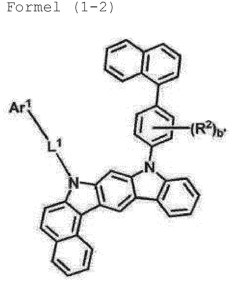 1) Ar1, L1 und R2 gleich wie in Anspruch 1 definiert sind,2) b' eine ganze Zahl von 1 bis 4 ist.
 - Verbindung nach Anspruch 1, wobei die durch die Formel (1) dargestellte Verbindung durch die Formel (1-3) dargestellt wird.
 1) Ar1, L1, R1 und R2 gleich wie in Anspruch 1 definiert sind,2) a' eine ganze Zahl von 1 bis 7 ist und b' eine ganze Zahl von 1 bis 4 ist.
 - Verbindung nach Anspruch 1, wobei L1 eine Einfachbindung; oder eine C6-C60-Arylengruppe ist; Ar1 eine C6-C18-Arylgruppe ist.
- Verbindung nach Anspruch 1, wobei die durch die Formel (1) dargestellte Verbindung durch die Formel (2-1) dargestellt wird.
 1) X O, S oder NRc ist,2) R3 und R4 jeweils unabhängig ausgewählt sind aus der Gruppe bestehend aus Wasserstoff; einer C6-C60-Arylgruppe; einer heterozyklischen C2-C60-Gruppe, die mindestens ein Heteroatom aus O, N, S, Si oder P beinhaltet; einer kondensierten Ring-Gruppe aus einem aliphatischen C3-C60-Ring und einem aromatischen C6-C60-Ring; einer C1-C50-Alkylgruppe, einer C2-C20-Alkenylgruppe, einer C2-C20-Alkinylgruppe; einer C1-C30-Alkoxygruppe, und einer C6-C30-Aryloxygruppe, und -L'-NRaRb; oder eine Vielzahl von benachbarten R3 oder eine Vielzahl von R4 aneinander gebunden sein können, um einen Ring zu bilden,3) c eine ganze Zahl von 0 bis 4 ist, d eine ganze Zahl von 0 bis 3 ist,4) L1, R1, R2, a, b, L', Ra und Rb gleich wie in Anspruch 1 definiert sind,5) Rc ausgewählt ist aus der Gruppe bestehend aus einem Wasserstoff; einer C6-C60-Arylgruppe; einer Fluorenyl-Gruppe; einer heterozyklischen C2-C60-Gruppe, die mindestens ein Heteroatom aus O, N, S, Si oder P beinhaltet; einer kondensierten Ring-Gruppe aus einem aliphatischen C3-C60-Ring und einem aromatischen C6-C60-Ring; einer C1-C60-Alkylgruppe, einer C2-C20-Alkenylgruppe, einer C2-C20-Alkinylgruppe, einer C1-C30-Alkoxygruppe und einer C6-C30-Aryloxygruppe.
 - Verbindung nach Anspruch 1, wobei der ΔEst-Wert der durch die Formel (1) dargestellten Verbindung 0,2100 oder weniger beträgt.
- Verbindung nach Anspruch 1, wobei der ΔEst-Wert der durch die Formel (1) dargestellten Verbindung 0,150 bis 0,2100 beträgt.
- Verbindung nach Anspruch 1, wobei Formel (1) durch eine beliebige der folgenden Verbindungen P-1 bis P-60 dargestellt wird:


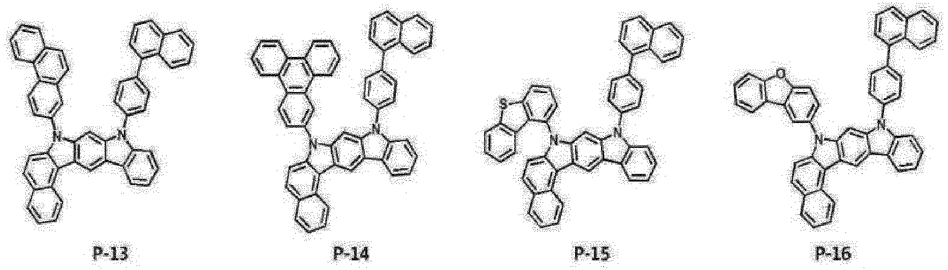


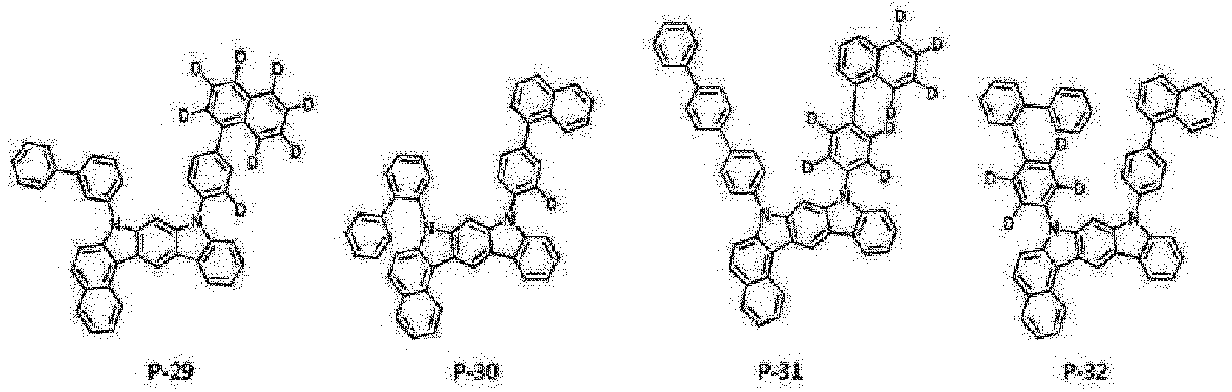
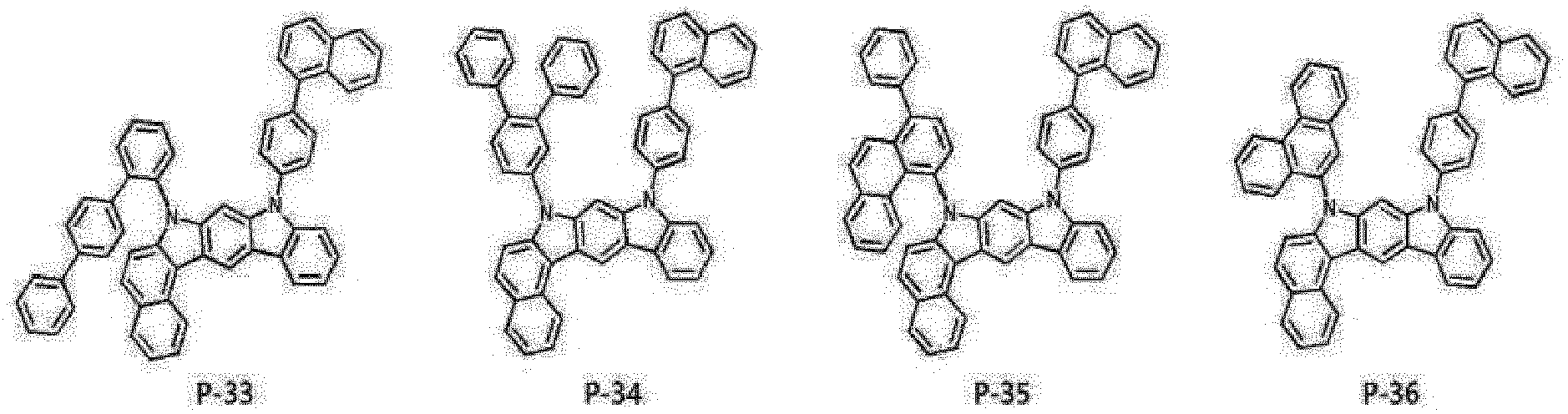


- Organisches elektronisches Element, umfassend eine Anode, eine Kathode und eine organische Materialschicht, die zwischen der Anode und der Kathode gebildet ist, wobei die organische Materialschicht eine einzelne Verbindung oder 2 oder mehr Verbindungen umfasst, die durch die Formel (1) nach Anspruch 1 dargestellt werden.
- Organisches elektronisches Element nach Anspruch 10, wobei die organische Materialschicht mindestens eine von einer Lochinjektionsschicht, einer Lochtransportschicht, einer Auslass-Hilfsschicht, einer emittierenden Schicht, einer Elektronentransport-Hilfsschicht, einer Elektronentransportschicht und einer Elektroneninjektionsschicht umfasst.
- Organisches elektronisches Element nach Anspruch 10, wobei die organische Materialschicht eine emittierende Schicht ist.
- Organisches elektronisches Element nach Anspruch 10, ferner umfassend eine Lichteffizienz-verbessernde Schicht, die auf mindestens einer der organischen Materialschicht entgegengesetzten Oberfläche aus einer Oberfläche der Anode und der Kathode gebildet ist.
- Organisches elektronisches Element nach Anspruch 10, wobei die organische Materialschicht mindestens 2 oder mehr Stapel beinhaltet, die eine Lochtransportschicht, eine emittierende Schicht und eine Elektronentransportschicht beinhalten, die der Reihe nach auf der Anode gebildet sind.
- Organisches elektronisches Element nach Anspruch 10, wobei die organische Materialschicht ferner eine ladungserzeugende Schicht umfasst, die zwischen den 2 oder mehr Stapeln gebildet ist.
- Elektronische Vorrichtung umfassend: eine Anzeigevorrichtung, die das organische elektronische Element nach Anspruch 10 beinhaltet; und eine Steuereinheit zum Ansteuern der Anzeigevorrichtung.
- Organisches elektronisches Element nach Anspruch 16, wobei das organische elektronische Element eines von einer organischen Elektrolumineszenz-Vorrichtung (OLED), einer organischen Solarzelle, einem organischen Fotorezeptor (OPC), einem organischen Transistor (organischer TFT), und einem Element für die monochrome oder weiße Beleuchtung ist.
Applications Claiming Priority (1)
| Application Number | Priority Date | Filing Date | Title |
|---|---|---|---|
| KR1020210103124A KR102303190B1 (ko) | 2021-08-05 | 2021-08-05 | 유기전기소자용 화합물, 이를 이용한 유기전기소자 및 그 전자 장치 |
Publications (2)
| Publication Number | Publication Date |
|---|---|
| EP4130002A1 EP4130002A1 (de) | 2023-02-08 |
| EP4130002B1 true EP4130002B1 (de) | 2023-07-12 |
Family
ID=77923954
Family Applications (1)
| Application Number | Title | Priority Date | Filing Date |
|---|---|---|---|
| EP21202077.0A Active EP4130002B1 (de) | 2021-08-05 | 2021-10-12 | Verbindung für organisches elektronisches element, organisches elektronisches element damit und elektronische vorrichtung dafür |
Country Status (4)
| Country | Link |
|---|---|
| US (1) | US11329235B1 (de) |
| EP (1) | EP4130002B1 (de) |
| KR (1) | KR102303190B1 (de) |
| CN (1) | CN115703782B (de) |
Families Citing this family (4)
| Publication number | Priority date | Publication date | Assignee | Title |
|---|---|---|---|---|
| KR20230164900A (ko) * | 2022-05-26 | 2023-12-05 | 덕산네오룩스 주식회사 | 유기전기소자용 화합물, 이를 이용한 유기전기소자 및 그 전자 장치 |
| KR20240024392A (ko) * | 2022-08-16 | 2024-02-26 | 덕산네오룩스 주식회사 | 유기전기 소자용 화합물, 이를 이용한 유기전기소자 및 그 전자 장치 |
| CN118724852A (zh) * | 2024-06-13 | 2024-10-01 | 阜阳欣奕华新材料科技股份有限公司 | 一种含二苯并五元杂环取代基的蒽类化合物、中间体和有机电致发光器件 |
| CN119899193A (zh) * | 2025-01-12 | 2025-04-29 | 西北工业大学 | 一种基于二芳基并咔唑材料的制备方法 |
Family Cites Families (8)
| Publication number | Priority date | Publication date | Assignee | Title |
|---|---|---|---|---|
| KR20170075877A (ko) * | 2015-12-23 | 2017-07-04 | 삼성디스플레이 주식회사 | 유기 발광 소자 |
| KR102697017B1 (ko) * | 2017-09-22 | 2024-08-22 | 듀폰스페셜티머터리얼스코리아 유한회사 | 복수 종의 호스트 재료 및 이를 포함하는 유기 전계 발광 소자 |
| WO2019059695A1 (en) * | 2017-09-22 | 2019-03-28 | Rohm And Haas Electronic Materials Korea Ltd. | PLURALITY OF HOST MATERIALS AND ORGANIC ELECTROLUMINESCENT DEVICE COMPRISING THE SAME |
| WO2019245164A1 (en) * | 2018-06-22 | 2019-12-26 | Rohm And Haas Electronic Materials Korea Ltd. | A plurality of host materials and organic electroluminescent device comprising the same |
| KR102244170B1 (ko) * | 2018-08-29 | 2021-04-26 | 롬엔드하스전자재료코리아유한회사 | 복수 종의 호스트 재료 및 이를 포함하는 유기 전계 발광 소자 |
| CN120774924A (zh) * | 2018-08-29 | 2025-10-14 | 杜邦特种材料韩国有限公司 | 多种主体材料和包含其的有机电致发光装置 |
| KR102888006B1 (ko) * | 2019-07-01 | 2025-11-24 | 듀폰스페셜티머터리얼스코리아 유한회사 | 유기 전계 발광 화합물 및 이를 포함하는 유기 전계 발광 소자 |
| CN113228336B (zh) * | 2019-10-01 | 2025-06-10 | 株式会社Lg化学 | 有机发光器件 |
-
2021
- 2021-08-05 KR KR1020210103124A patent/KR102303190B1/ko active Active
- 2021-10-12 EP EP21202077.0A patent/EP4130002B1/de active Active
- 2021-11-08 CN CN202111312188.XA patent/CN115703782B/zh active Active
- 2021-11-11 US US17/454,599 patent/US11329235B1/en active Active
Also Published As
| Publication number | Publication date |
|---|---|
| EP4130002A1 (de) | 2023-02-08 |
| CN115703782B (zh) | 2024-04-19 |
| CN115703782A (zh) | 2023-02-17 |
| US11329235B1 (en) | 2022-05-10 |
| KR102303190B1 (ko) | 2021-09-17 |
Similar Documents
| Publication | Publication Date | Title |
|---|---|---|
| US12439818B2 (en) | Compound for organic electronic element, organic electronic element using the same, and an electronic device thereof | |
| CN115943749B (zh) | 用于有机电气元件的化合物、使用所述化合物的有机电气元件、以及包括所述有机电气元件的电子装置 | |
| KR102373387B1 (ko) | 유기전기소자용 화합물, 이를 이용한 유기전기소자 및 그 전자 장치 | |
| CN116396282B (zh) | 用于有机电气元件的化合物、使用所述化合物的有机电气元件及其电子装置 | |
| EP3990426B1 (de) | Verbindung für organisches elektronisches element, diese verwendendes organisches elektronisches element und entsprechende elektronische vorrichtung | |
| US20230140925A1 (en) | Compound for organic electrical element, organic electrical element using same, and electronic device comprising same | |
| EP4130002A1 (de) | Verbindung für organisches elektronisches element, organisches elektronisches element damit und elektronische vorrichtung dafür | |
| EP4137492B1 (de) | Verbindung für organisches elektronisches element, organisches elektronisches element damit und elektronische vorrichtung damit | |
| US20230165139A1 (en) | Compound for organic electric element, organic electric element using same, and electronic device thereof | |
| CN115023414B (zh) | 用于有机电元件的化合物、利用其的有机电元件及其电子装置 | |
| KR102793749B1 (ko) | 유기전기소자용 화합물, 이를 이용한 유기전기소자 및 그 전자 장치 | |
| KR102793764B1 (ko) | 유기전기소자용 화합물, 이를 이용한 유기전기소자 및 그 전자 장치 | |
| CN117545746A (zh) | 用于有机电气元件的化合物、使用所述化合物的有机电气元件及其电子装置 | |
| KR20200119503A (ko) | 유기전기 소자용 화합물, 이를 이용한 유기전기소자 및 그 전자 장치 | |
| CN115777242A (zh) | 包含用于有机电子元件的化合物的有机电子元件及其电子装置 | |
| KR20210128205A (ko) | 유기전기소자용 화합물, 이를 이용한 유기전기소자 및 그 전자 장치 | |
| KR102845606B1 (ko) | 유기전기소자용 화합물, 이를 이용한 유기전기소자 및 그 전자 장치 | |
| US20230104183A1 (en) | Compound for organic electrical element, organic electrical element using same, and electronic device thereof | |
| KR20210126493A (ko) | 유기전기소자용 화합물, 이를 이용한 유기전기소자 및 그 전자 장치 | |
| CN116583507B (zh) | 用于有机电子元件的化合物、使用所述化合物的有机电子元件及其电子装置 | |
| CN111315720A (zh) | 有机电气元件用化合物、利用其的有机电气元件及其电子装置 | |
| CN117203203A (zh) | 用于有机电气元件的化合物、使用所述化合物的有机电气元件及其电子装置 | |
| EP4159724A1 (de) | Verbindung für organisches elektronisches element, organisches elektronisches element damit und elektronische vorrichtung dafür | |
| US11316116B1 (en) | Compound for organic electronic element, organic electronic element using the same, and an electronic device thereof | |
| KR20220006291A (ko) | 유기전기소자용 화합물, 이를 이용한 유기전기소자 및 그 전자 장치 |
Legal Events
| Date | Code | Title | Description |
|---|---|---|---|
| PUAI | Public reference made under article 153(3) epc to a published international application that has entered the european phase |
Free format text: ORIGINAL CODE: 0009012 |
|
| STAA | Information on the status of an ep patent application or granted ep patent |
Free format text: STATUS: REQUEST FOR EXAMINATION WAS MADE |
|
| 17P | Request for examination filed |
Effective date: 20220419 |
|
| AK | Designated contracting states |
Kind code of ref document: A1 Designated state(s): AL AT BE BG CH CY CZ DE DK EE ES FI FR GB GR HR HU IE IS IT LI LT LU LV MC MK MT NL NO PL PT RO RS SE SI SK SM TR |
|
| GRAP | Despatch of communication of intention to grant a patent |
Free format text: ORIGINAL CODE: EPIDOSNIGR1 |
|
| STAA | Information on the status of an ep patent application or granted ep patent |
Free format text: STATUS: GRANT OF PATENT IS INTENDED |
|
| RIC1 | Information provided on ipc code assigned before grant |
Ipc: H10K 50/00 20230101ALI20230303BHEP Ipc: H10K 85/60 20230101ALI20230303BHEP Ipc: C07D 487/04 20060101AFI20230303BHEP |
|
| INTG | Intention to grant announced |
Effective date: 20230404 |
|
| GRAS | Grant fee paid |
Free format text: ORIGINAL CODE: EPIDOSNIGR3 |
|
| GRAA | (expected) grant |
Free format text: ORIGINAL CODE: 0009210 |
|
| STAA | Information on the status of an ep patent application or granted ep patent |
Free format text: STATUS: THE PATENT HAS BEEN GRANTED |
|
| AK | Designated contracting states |
Kind code of ref document: B1 Designated state(s): AL AT BE BG CH CY CZ DE DK EE ES FI FR GB GR HR HU IE IS IT LI LT LU LV MC MK MT NL NO PL PT RO RS SE SI SK SM TR |
|
| P01 | Opt-out of the competence of the unified patent court (upc) registered |
Effective date: 20230530 |
|
| REG | Reference to a national code |
Ref country code: CH Ref legal event code: EP |
|
| REG | Reference to a national code |
Ref country code: IE Ref legal event code: FG4D |
|
| REG | Reference to a national code |
Ref country code: DE Ref legal event code: R096 Ref document number: 602021003421 Country of ref document: DE |
|
| REG | Reference to a national code |
Ref country code: LT Ref legal event code: MG9D |
|
| REG | Reference to a national code |
Ref country code: NL Ref legal event code: MP Effective date: 20230712 |
|
| REG | Reference to a national code |
Ref country code: AT Ref legal event code: MK05 Ref document number: 1587040 Country of ref document: AT Kind code of ref document: T Effective date: 20230712 |
|
| PG25 | Lapsed in a contracting state [announced via postgrant information from national office to epo] |
Ref country code: NL Free format text: LAPSE BECAUSE OF FAILURE TO SUBMIT A TRANSLATION OF THE DESCRIPTION OR TO PAY THE FEE WITHIN THE PRESCRIBED TIME-LIMIT Effective date: 20230712 |
|
| PG25 | Lapsed in a contracting state [announced via postgrant information from national office to epo] |
Ref country code: GR Free format text: LAPSE BECAUSE OF FAILURE TO SUBMIT A TRANSLATION OF THE DESCRIPTION OR TO PAY THE FEE WITHIN THE PRESCRIBED TIME-LIMIT Effective date: 20231013 |
|
| PG25 | Lapsed in a contracting state [announced via postgrant information from national office to epo] |
Ref country code: ES Free format text: LAPSE BECAUSE OF FAILURE TO SUBMIT A TRANSLATION OF THE DESCRIPTION OR TO PAY THE FEE WITHIN THE PRESCRIBED TIME-LIMIT Effective date: 20230712 |
|
| PG25 | Lapsed in a contracting state [announced via postgrant information from national office to epo] |
Ref country code: IS Free format text: LAPSE BECAUSE OF FAILURE TO SUBMIT A TRANSLATION OF THE DESCRIPTION OR TO PAY THE FEE WITHIN THE PRESCRIBED TIME-LIMIT Effective date: 20231112 |
|
| PG25 | Lapsed in a contracting state [announced via postgrant information from national office to epo] |
Ref country code: SE Free format text: LAPSE BECAUSE OF FAILURE TO SUBMIT A TRANSLATION OF THE DESCRIPTION OR TO PAY THE FEE WITHIN THE PRESCRIBED TIME-LIMIT Effective date: 20230712 Ref country code: RS Free format text: LAPSE BECAUSE OF FAILURE TO SUBMIT A TRANSLATION OF THE DESCRIPTION OR TO PAY THE FEE WITHIN THE PRESCRIBED TIME-LIMIT Effective date: 20230712 Ref country code: PT Free format text: LAPSE BECAUSE OF FAILURE TO SUBMIT A TRANSLATION OF THE DESCRIPTION OR TO PAY THE FEE WITHIN THE PRESCRIBED TIME-LIMIT Effective date: 20231113 Ref country code: NO Free format text: LAPSE BECAUSE OF FAILURE TO SUBMIT A TRANSLATION OF THE DESCRIPTION OR TO PAY THE FEE WITHIN THE PRESCRIBED TIME-LIMIT Effective date: 20231012 Ref country code: LV Free format text: LAPSE BECAUSE OF FAILURE TO SUBMIT A TRANSLATION OF THE DESCRIPTION OR TO PAY THE FEE WITHIN THE PRESCRIBED TIME-LIMIT Effective date: 20230712 Ref country code: LT Free format text: LAPSE BECAUSE OF FAILURE TO SUBMIT A TRANSLATION OF THE DESCRIPTION OR TO PAY THE FEE WITHIN THE PRESCRIBED TIME-LIMIT Effective date: 20230712 Ref country code: IS Free format text: LAPSE BECAUSE OF FAILURE TO SUBMIT A TRANSLATION OF THE DESCRIPTION OR TO PAY THE FEE WITHIN THE PRESCRIBED TIME-LIMIT Effective date: 20231112 Ref country code: HR Free format text: LAPSE BECAUSE OF FAILURE TO SUBMIT A TRANSLATION OF THE DESCRIPTION OR TO PAY THE FEE WITHIN THE PRESCRIBED TIME-LIMIT Effective date: 20230712 Ref country code: GR Free format text: LAPSE BECAUSE OF FAILURE TO SUBMIT A TRANSLATION OF THE DESCRIPTION OR TO PAY THE FEE WITHIN THE PRESCRIBED TIME-LIMIT Effective date: 20231013 Ref country code: FI Free format text: LAPSE BECAUSE OF FAILURE TO SUBMIT A TRANSLATION OF THE DESCRIPTION OR TO PAY THE FEE WITHIN THE PRESCRIBED TIME-LIMIT Effective date: 20230712 Ref country code: ES Free format text: LAPSE BECAUSE OF FAILURE TO SUBMIT A TRANSLATION OF THE DESCRIPTION OR TO PAY THE FEE WITHIN THE PRESCRIBED TIME-LIMIT Effective date: 20230712 Ref country code: AT Free format text: LAPSE BECAUSE OF FAILURE TO SUBMIT A TRANSLATION OF THE DESCRIPTION OR TO PAY THE FEE WITHIN THE PRESCRIBED TIME-LIMIT Effective date: 20230712 |
|
| PG25 | Lapsed in a contracting state [announced via postgrant information from national office to epo] |
Ref country code: PL Free format text: LAPSE BECAUSE OF FAILURE TO SUBMIT A TRANSLATION OF THE DESCRIPTION OR TO PAY THE FEE WITHIN THE PRESCRIBED TIME-LIMIT Effective date: 20230712 |
|
| REG | Reference to a national code |
Ref country code: DE Ref legal event code: R097 Ref document number: 602021003421 Country of ref document: DE |
|
| PG25 | Lapsed in a contracting state [announced via postgrant information from national office to epo] |
Ref country code: SM Free format text: LAPSE BECAUSE OF FAILURE TO SUBMIT A TRANSLATION OF THE DESCRIPTION OR TO PAY THE FEE WITHIN THE PRESCRIBED TIME-LIMIT Effective date: 20230712 Ref country code: RO Free format text: LAPSE BECAUSE OF FAILURE TO SUBMIT A TRANSLATION OF THE DESCRIPTION OR TO PAY THE FEE WITHIN THE PRESCRIBED TIME-LIMIT Effective date: 20230712 Ref country code: EE Free format text: LAPSE BECAUSE OF FAILURE TO SUBMIT A TRANSLATION OF THE DESCRIPTION OR TO PAY THE FEE WITHIN THE PRESCRIBED TIME-LIMIT Effective date: 20230712 Ref country code: DK Free format text: LAPSE BECAUSE OF FAILURE TO SUBMIT A TRANSLATION OF THE DESCRIPTION OR TO PAY THE FEE WITHIN THE PRESCRIBED TIME-LIMIT Effective date: 20230712 Ref country code: CZ Free format text: LAPSE BECAUSE OF FAILURE TO SUBMIT A TRANSLATION OF THE DESCRIPTION OR TO PAY THE FEE WITHIN THE PRESCRIBED TIME-LIMIT Effective date: 20230712 Ref country code: SK Free format text: LAPSE BECAUSE OF FAILURE TO SUBMIT A TRANSLATION OF THE DESCRIPTION OR TO PAY THE FEE WITHIN THE PRESCRIBED TIME-LIMIT Effective date: 20230712 |
|
| PLBE | No opposition filed within time limit |
Free format text: ORIGINAL CODE: 0009261 |
|
| STAA | Information on the status of an ep patent application or granted ep patent |
Free format text: STATUS: NO OPPOSITION FILED WITHIN TIME LIMIT |
|
| PG25 | Lapsed in a contracting state [announced via postgrant information from national office to epo] |
Ref country code: IT Free format text: LAPSE BECAUSE OF FAILURE TO SUBMIT A TRANSLATION OF THE DESCRIPTION OR TO PAY THE FEE WITHIN THE PRESCRIBED TIME-LIMIT Effective date: 20230712 Ref country code: MC Free format text: LAPSE BECAUSE OF FAILURE TO SUBMIT A TRANSLATION OF THE DESCRIPTION OR TO PAY THE FEE WITHIN THE PRESCRIBED TIME-LIMIT Effective date: 20230712 |
|
| REG | Reference to a national code |
Ref country code: BE Ref legal event code: MM Effective date: 20231031 |
|
| 26N | No opposition filed |
Effective date: 20240415 |
|
| PG25 | Lapsed in a contracting state [announced via postgrant information from national office to epo] |
Ref country code: LU Free format text: LAPSE BECAUSE OF NON-PAYMENT OF DUE FEES Effective date: 20231012 |
|
| PG25 | Lapsed in a contracting state [announced via postgrant information from national office to epo] |
Ref country code: LU Free format text: LAPSE BECAUSE OF NON-PAYMENT OF DUE FEES Effective date: 20231012 |
|
| PG25 | Lapsed in a contracting state [announced via postgrant information from national office to epo] |
Ref country code: SI Free format text: LAPSE BECAUSE OF FAILURE TO SUBMIT A TRANSLATION OF THE DESCRIPTION OR TO PAY THE FEE WITHIN THE PRESCRIBED TIME-LIMIT Effective date: 20230712 |
|
| PG25 | Lapsed in a contracting state [announced via postgrant information from national office to epo] |
Ref country code: BE Free format text: LAPSE BECAUSE OF NON-PAYMENT OF DUE FEES Effective date: 20231031 |
|
| PG25 | Lapsed in a contracting state [announced via postgrant information from national office to epo] |
Ref country code: IE Free format text: LAPSE BECAUSE OF NON-PAYMENT OF DUE FEES Effective date: 20231012 |
|
| PG25 | Lapsed in a contracting state [announced via postgrant information from national office to epo] |
Ref country code: IE Free format text: LAPSE BECAUSE OF NON-PAYMENT OF DUE FEES Effective date: 20231012 |
|
| PG25 | Lapsed in a contracting state [announced via postgrant information from national office to epo] |
Ref country code: BG Free format text: LAPSE BECAUSE OF FAILURE TO SUBMIT A TRANSLATION OF THE DESCRIPTION OR TO PAY THE FEE WITHIN THE PRESCRIBED TIME-LIMIT Effective date: 20230712 |
|
| PG25 | Lapsed in a contracting state [announced via postgrant information from national office to epo] |
Ref country code: BG Free format text: LAPSE BECAUSE OF FAILURE TO SUBMIT A TRANSLATION OF THE DESCRIPTION OR TO PAY THE FEE WITHIN THE PRESCRIBED TIME-LIMIT Effective date: 20230712 |
|
| REG | Reference to a national code |
Ref country code: CH Ref legal event code: PL |
|
| PG25 | Lapsed in a contracting state [announced via postgrant information from national office to epo] |
Ref country code: CH Free format text: LAPSE BECAUSE OF NON-PAYMENT OF DUE FEES Effective date: 20241031 |
|
| PG25 | Lapsed in a contracting state [announced via postgrant information from national office to epo] |
Ref country code: CY Free format text: LAPSE BECAUSE OF FAILURE TO SUBMIT A TRANSLATION OF THE DESCRIPTION OR TO PAY THE FEE WITHIN THE PRESCRIBED TIME-LIMIT; INVALID AB INITIO Effective date: 20211012 |
|
| PG25 | Lapsed in a contracting state [announced via postgrant information from national office to epo] |
Ref country code: TR Free format text: LAPSE BECAUSE OF FAILURE TO SUBMIT A TRANSLATION OF THE DESCRIPTION OR TO PAY THE FEE WITHIN THE PRESCRIBED TIME-LIMIT Effective date: 20230712 |
|
| PGFP | Annual fee paid to national office [announced via postgrant information from national office to epo] |
Ref country code: DE Payment date: 20251021 Year of fee payment: 5 |
|
| PGFP | Annual fee paid to national office [announced via postgrant information from national office to epo] |
Ref country code: GB Payment date: 20251022 Year of fee payment: 5 |
|
| PGFP | Annual fee paid to national office [announced via postgrant information from national office to epo] |
Ref country code: FR Payment date: 20251030 Year of fee payment: 5 |
|
| PG25 | Lapsed in a contracting state [announced via postgrant information from national office to epo] |
Ref country code: HU Free format text: LAPSE BECAUSE OF FAILURE TO SUBMIT A TRANSLATION OF THE DESCRIPTION OR TO PAY THE FEE WITHIN THE PRESCRIBED TIME-LIMIT; INVALID AB INITIO Effective date: 20211012 |